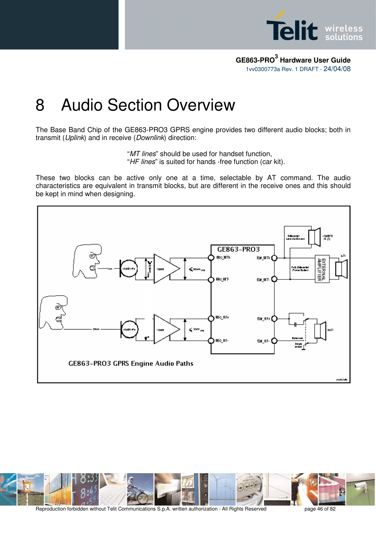
Telit Communications S p A 863P3 Quad-Band GSM/GPRS module -Model: GE863-PRO3 User Manual Manual
Telit Communications S.p.A. Quad-Band GSM/GPRS module -Model: GE863-PRO3 Manual
UserManual.wiki
>
Telit Communications S p A
>
863P3 User Manual
Manual
Navigation menu
Upload a User Manual
Namespaces
Wiki Guide
HTML
PDF
Info
Views
User Manual
Discussion / Help
Navigation


![GE863-PRO3 Hardware User Guide 1vv0300773a Rev. 1 DRAFT - 24/04/08 Reproduction forbidden without Telit Communications S.p.A. written authorization - All Rights Reserved page 37 of 82 6.3 GSM Antenna - installation Guidelines • Install the antenna in a place covered by the GSM signal. • The Antenna must be installed to provide a separation distance of at least 20 cm from all persons and must not be co-located or operating in conjunction with any other antenna or transmitter; • Antenna shall not be installed inside metal cases • Antenna shall be installed also according Antenna manufacturer instructions. 6.4 Electro Magnetic Interference - Guidelines The GE863-PRO3 has been particularly designed in order to keep to a minimum the Electro Magnetic Interferences between the ARM part and the GSM/GPRS engine, however especially the ARM part remains a noisy device that must be threaten with care in order to avoid that its EMI affect the GPRS part through an external coupling. Therefore: • Keep fast ARM lines far away from Antenna line in order to avoid direct coupling; • Keep fast ARM lines buried in the inner layers, with Ground Layers [fenced with vias] on the top/bottom layers; • If your lines are long, place a series resistor [ in the range of 47Ω – 100 Ω ] close to the GE863-PRO3 ARM ball to reduce the ringing and the EM emissions of the signal • If your PCB lines are very long, place a terminator resistor close to the device line end.](https://usermanual.wiki/Telit-Communications-S-p-A/863P3/User-Guide-941147-Page-37.png)

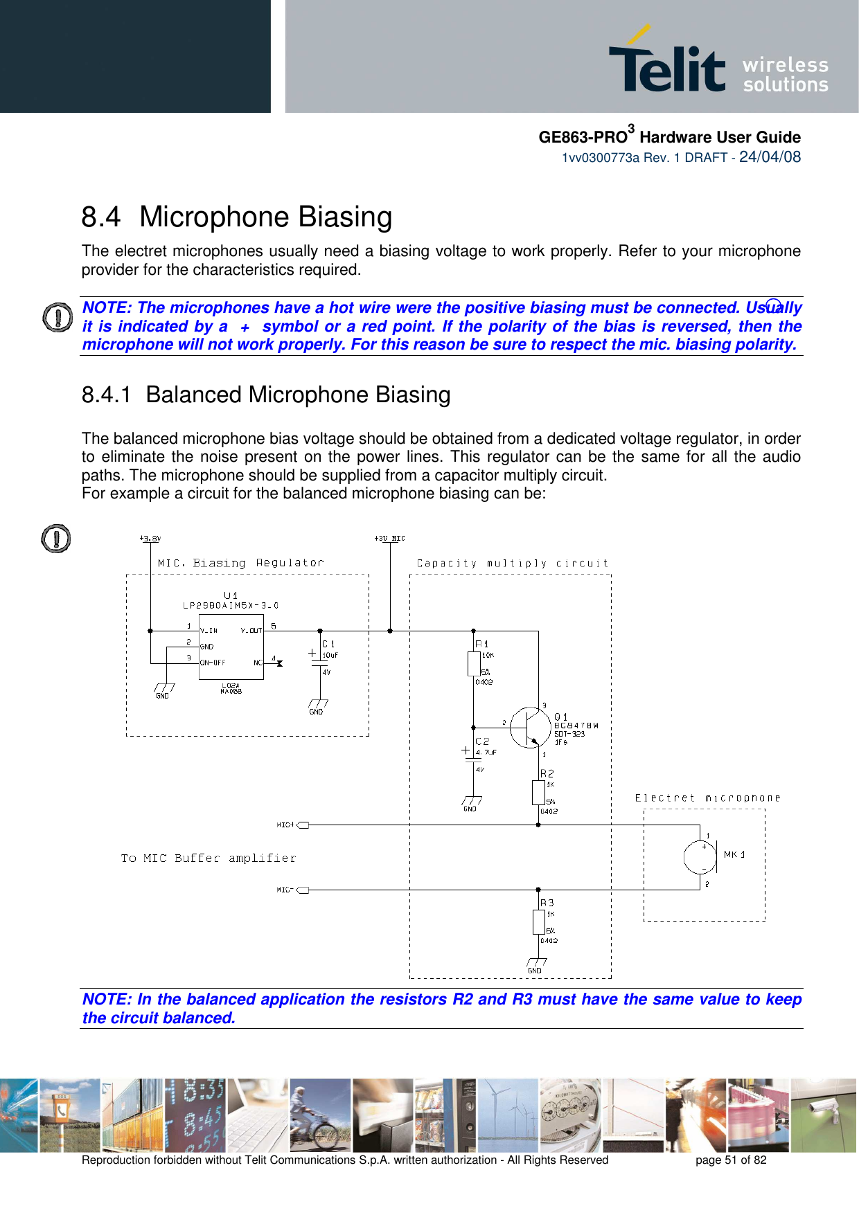
![GE863-PRO3 Hardware User Guide 1vv0300773a Rev. 1 DRAFT - 24/04/08 Reproduction forbidden without Telit Communications S.p.A. written authorization - All Rights Reserved page 48 of 82 TIP: definition of the nominal sensitivity of the microphone lines . The nominal sensitivity of the microphone lines indicates the voltage level on the GE863-PRO3 pins present during "normal spoken" conditions. For a handset , the "normal spoken” conditions take place when the talker mouth is 7cm far from the microphone ; under these conditions the voice will produce an acoustic pressure of -4,7dBPa @1kHz on the microphone membrane . TIP: electrical equivalent signal and operating voice levels . At "normal spoken" conditions, a microphone having the suggested nominal sensitivity of -45dBVrms/Pa , will produce the electrical equivalent signal : that means : During a call, this level varies according to the volume of the talker voice; usually the following rough thumb rule for the dynamic range may be used : 1) the talker is screaming . This is the strongest voice level condition: the signal increases by +20dB; 2) the talker is whispering. This is the lowest voice level condition: the voice level decreases by –50dB. These changes must be considered for designing the external microphone amplifier. TIP: example of external microphone amplifier calculation . Let’s suppose to use the 1stdifferential microphone path .In this case the maximum differential input voltage to “Mic_MT” lines is 365mVrms(1,03Vpp) corresponding to –8,76dBV. Now we can calculate the maximum voltage gain of an external microphone amplifier GA : ()[]dBVGdBMicLevelA76,820 −=++ []76,8207,49 −=++−AG AG−=+− 209,40 dBGA94,20= you can set GA= +20dB to use standard resistor values . MicLevel = ( -45) + (-4.7) = -49.7 dBVrms MicVoltage = 10 ( -49.7 / 20 ) = 3.3* 10 -3 Vrms](https://usermanual.wiki/Telit-Communications-S-p-A/863P3/User-Guide-941147-Page-48.png)

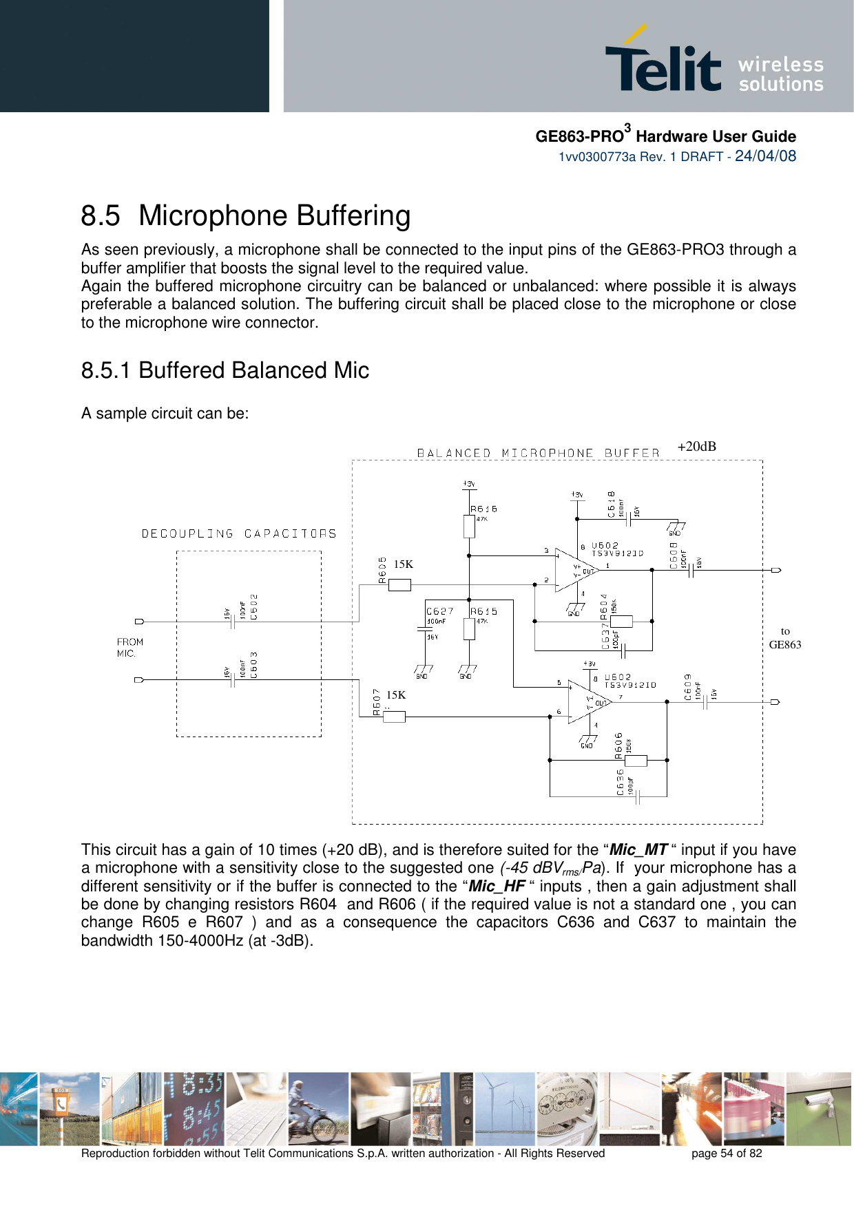
![GE863-PRO3 Hardware User Guide 1vv0300773a Rev. 1 DRAFT - 24/04/08 Reproduction forbidden without Telit Communications S.p.A. written authorization - All Rights Reserved page 55 of 82 The buffer gain is given by the formula: 607606605604RRRRGain == The C636 and C637 capacitors are placed in order to cut off the gain at higher frequencies than the transmitted GSM band, the cutoff frequency (-3dB) should be 3500Hz in order to have -1dB at 3kHz. The cutoff frequency is given by the formula: 636*606*21637*604*21.CRCRfreqππ== [Hz] TIP: example of calculation . Let's assume you have a microphone with a sensitivity of -45 dBVrms/Pa and you want to use it in 1st differential microphone path (“Mic_MT” inputs) in "normal spoken" conditions at acoustic pressure of -4.7dBPa. As reported at page 33 , the electrical level output from the microphone will be : corresponding to: When the talker is screaming ,we will have a signal of 330 mVrms on the “Mic_MT “ inputs due to a 20dB higher Mic Level (see TIP 1) with a buffer gain GA : GA =20 log (AmplifierOutput / MicVoltage) =20 log (330 * 10 -3 )/( 33 * 10 -3 ) = 20 log 10=20dB The corresponding values for the resistors on the buffer could be ( if we keep the input resistance 10kΩ ) R604 = R606 = gain* R607= gain* R605 = 10* 15 = 150 kΩ The commercial values of 150kΩ & 15kΩ are then chosen. As a consequence the values of the capacitors C636 and C637 shall be: C636=C637= 1/ (2π*4000*R606)= 265 *10 -12 F A commercial value of 270pF gives a cutoff frequency of 3931Hz with an errorless than 1,8% . MicLevel = ( -45) + (-4.7) = -49.7 dBVrms MicVoltage = 10 ( -49.7 / 20 ) = 3.3* 10 -3 Vrms](https://usermanual.wiki/Telit-Communications-S-p-A/863P3/User-Guide-941147-Page-55.png)
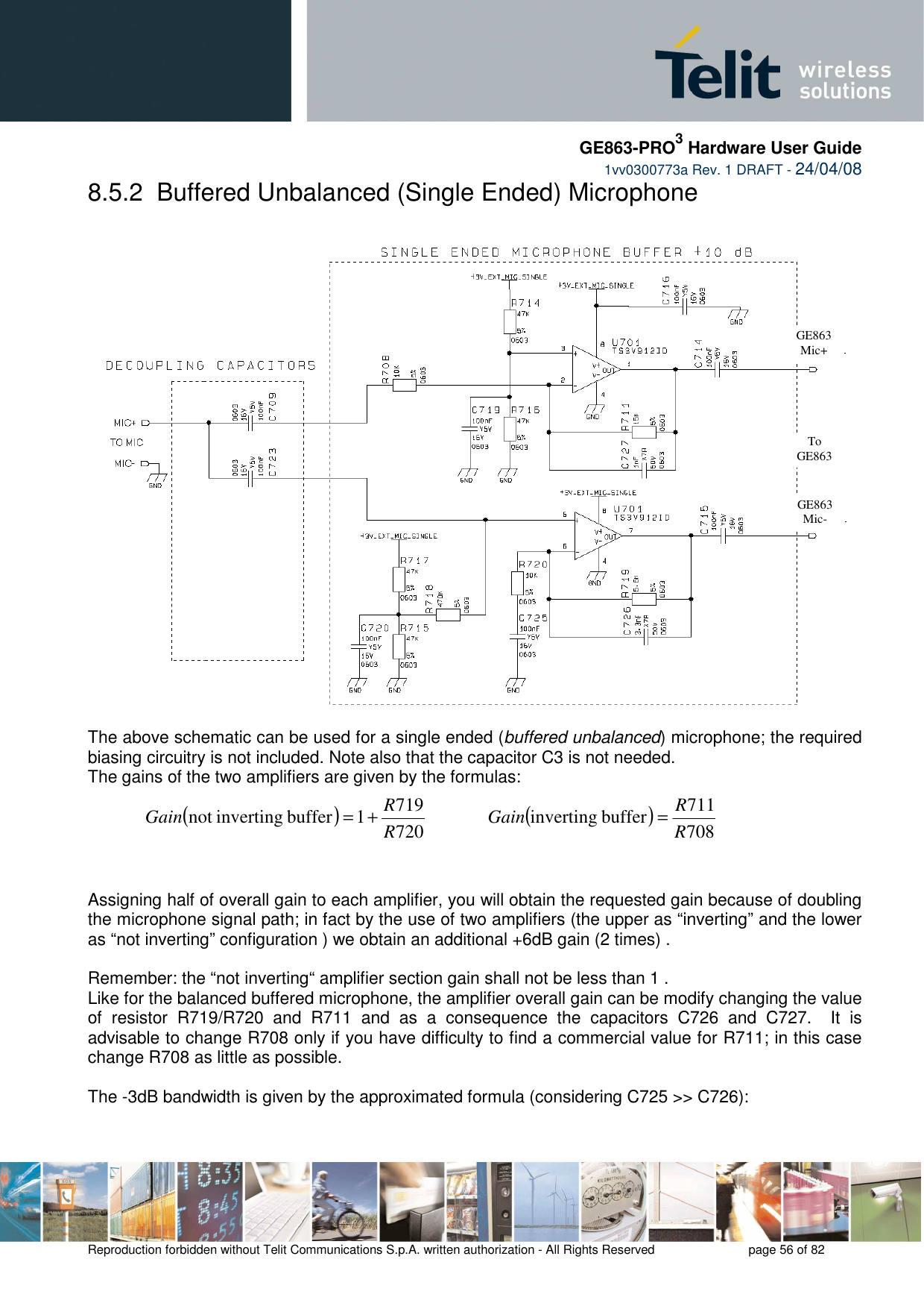
![GE863-PRO3 Hardware User Guide 1vv0300773a Rev. 1 DRAFT - 24/04/08 Reproduction forbidden without Telit Communications S.p.A. written authorization - All Rights Reserved page 57 of 82 727*711*21726*719*21.CRCRfreqππ== [Hz] The buffer bandwidth at -3dB shall be 4KHz. Note that the biasing of the operational amplifier is given for the inverting amplifier by the series divider R714-R715. The 100nF capacitor C719 is needed to filter the noise that could be coupled to that divider. For the not inverting operational amplifier the biasing is given by a different divider R715-R717 with the capacitor C720 and through a series resistor R718 of 470KΩ. TIP: example of calculation. Llet's assume you have a microphone with a sensitivity of -45dBVrms/Pa and you want to use it in 2nd differential microphone path (“Mic_HF” inputs) in "normal spoken" conditions at acoustic pressure of -4.7dBPa. As reported at page XX , the electrical level output from the microphone will be : but we have to consider 20dB loss due to the higher distance from the mouth of the talker ( 50cm ) . corresponding to In order to have a signal of 1 mVrms at the “Mic_HF” inputs , as suggested at TIP “environment consideration “, the buffer must have a gain or +10 dB Keeping in mind that “ balancing the line will double the signal”, to calculate the resistor values assign half of required gain GA to each amplifier section . And therefore GS =1,5times (or +3,52dB) . Choosing as 10kΩ as the input resistance , the corresponding values for the resistors on the buffer will be : R711 = GS * R708= 1.5*10 =15 kΩ R719 = (GS -1) * R720 = (1.5 -1)*10 =5 kΩ The commercial values of 15kΩ and 5.6kΩ be accepted . As a consequence of the assigned values of the resistors, the nominal values of C726 and C727 are : MicLevel = ( -45) + (-4.7) = -49.7 dBVrms MicVoltage = 10 ( -69.7 / 20 ) = 0,33* 10 -3 V MicLevel = ( -49.7) + (-20) = -69.7 dBVrms GA= “Mic_HF /MicVoltage = (1*10 -3)/(0,33*10 -3)=3](https://usermanual.wiki/Telit-Communications-S-p-A/863P3/User-Guide-941147-Page-57.png)

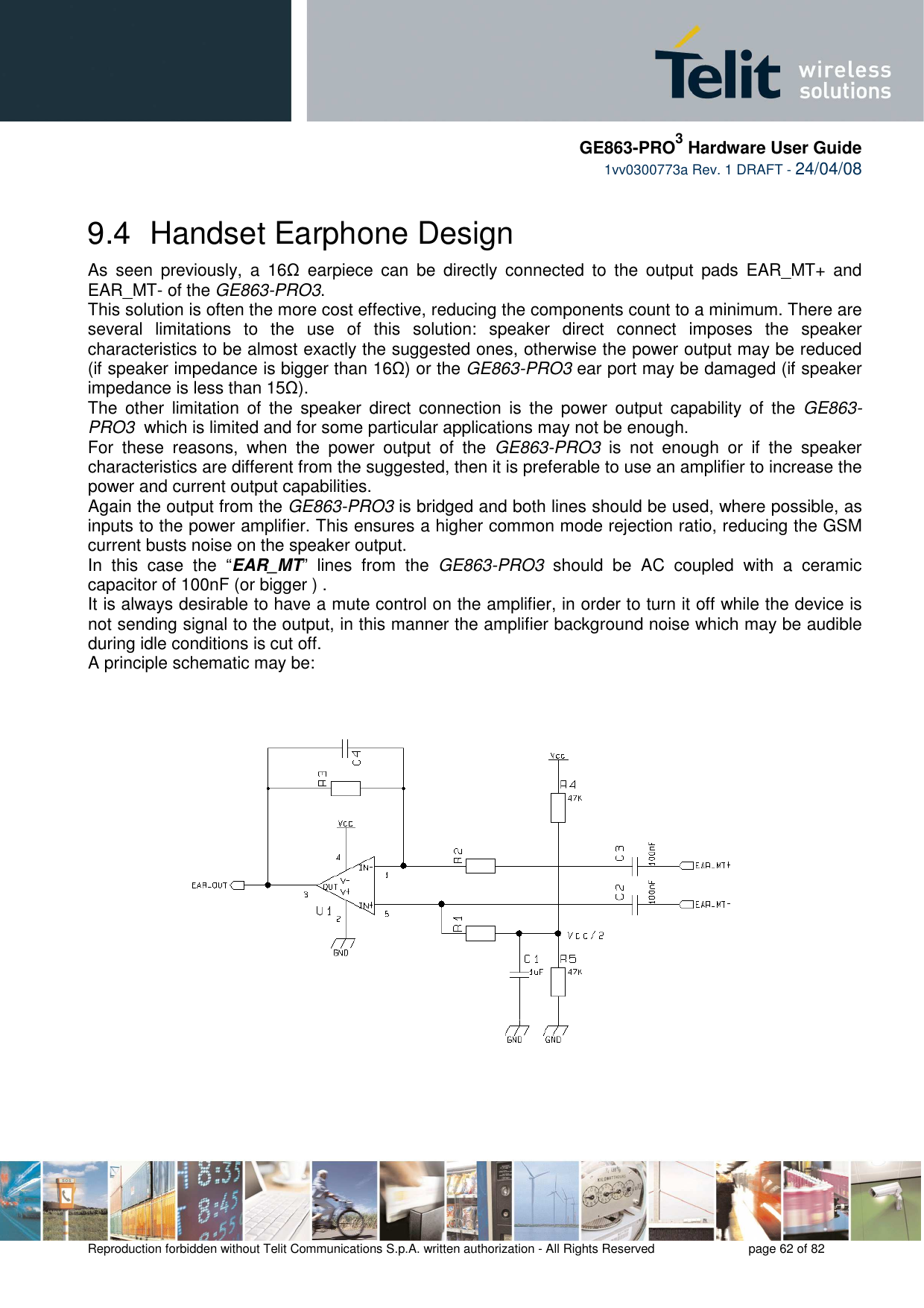
![GE863-PRO3 Hardware User Guide 1vv0300773a Rev. 1 DRAFT - 24/04/08 Reproduction forbidden without Telit Communications S.p.A. written authorization - All Rights Reserved page 63 of 82 The resulting gain and high pass cut can be obtained with the formula: 23RRGain = 4*3*21.CRfreqπ= [Hz] And an example of internal Ear amplifier could be: Some amplifier require a low impedance load at high frequency in order to avoid auto oscillation, this can be made with a capacitor (100nF) in series with a resistor (15Ω). When designing your application, remember to provide an adequate bypass capacitor to the amplifier and place it close to the power input pin of the IC, keeping the traces as short as possible. 9.5 Hands-Free Earphone (Low Power) Design The same design considerations made for the handset are valid for the hands-free earphone. +12dB GE863-PRO3](https://usermanual.wiki/Telit-Communications-S-p-A/863P3/User-Guide-941147-Page-63.png)


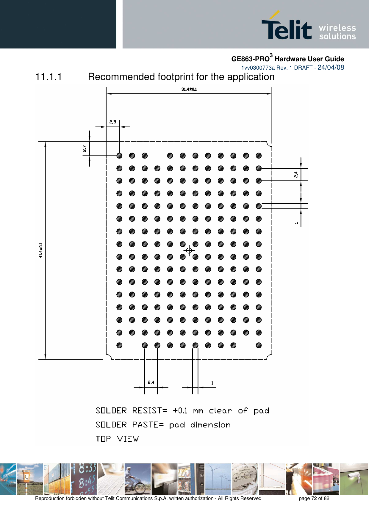
![GE863-PRO3 Hardware User Guide 1vv0300773a Rev. 1 DRAFT - 24/04/08 Reproduction forbidden without Telit Communications S.p.A. written authorization - All Rights Reserved page 73 of 82 11.1.2 Stencil Stencil’s apertures layout can be the same of the recommended footprint (1:1), we suggest a thickness of stencil foil ≥ 120µm. 11.1.3 PCB pad Design “Non solder mask defined” (NSMD) type is recommended for the solder pads on the PCB. Recommendations for PCB pad dimensions Ball pitch [mm] 2,4 Solder resist opening diameter A [mm] 1,10 Metal pad diameter B [mm] 1 ± 0.05 Placement of microvias not covered by solder resist is not recommended inside the “Solder resist opening”, unless the microvia carry the same signal of the pad itself.](https://usermanual.wiki/Telit-Communications-S-p-A/863P3/User-Guide-941147-Page-73.png)
![GE863-PRO3 Hardware User Guide 1vv0300773a Rev. 1 DRAFT - 24/04/08 Reproduction forbidden without Telit Communications S.p.A. written authorization - All Rights Reserved page 74 of 82 Holes in pad are allowed only for blind holes and not for through holes. Recommendations for PCB pad surfaces: Finish Layer thickness [µm] Properties Electro-less Ni / Immersion Au 3 –7 / 0.05 – 0.15 good solder ability protection, high shear force values The PCB must be able to resist the higher temperatures, which are occurring at the lead-free process. This issue should be discussed with the PCB-supplier. Generally, the wet-ability of tin-lead solder paste on the described surface plating is better compared to lead-free solder paste. 11.1.4 Solder paste Lead free Solder paste Sn/Ag/Cu](https://usermanual.wiki/Telit-Communications-S-p-A/863P3/User-Guide-941147-Page-74.png)


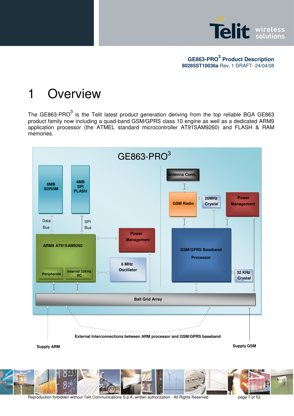


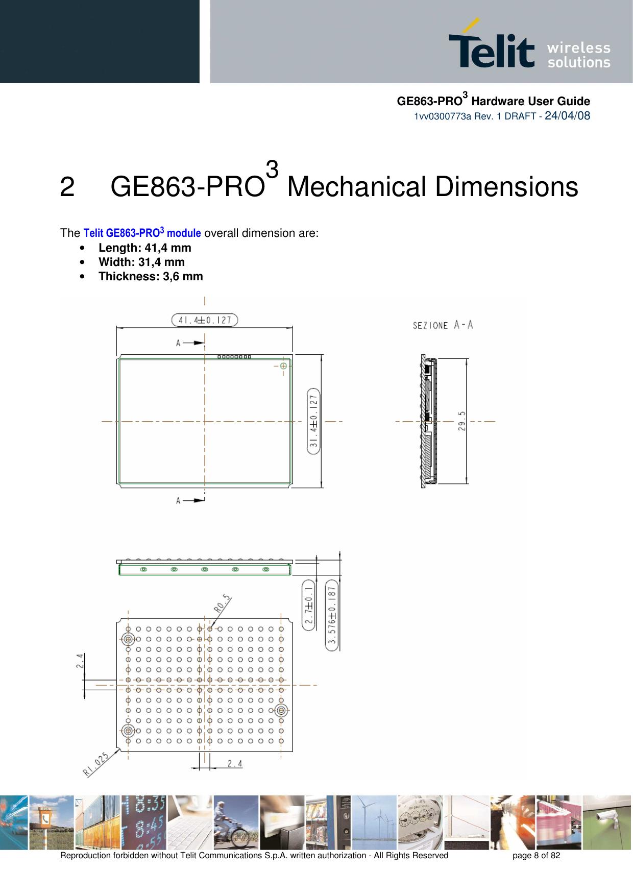
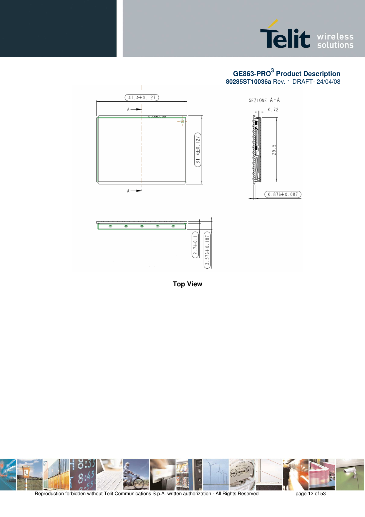
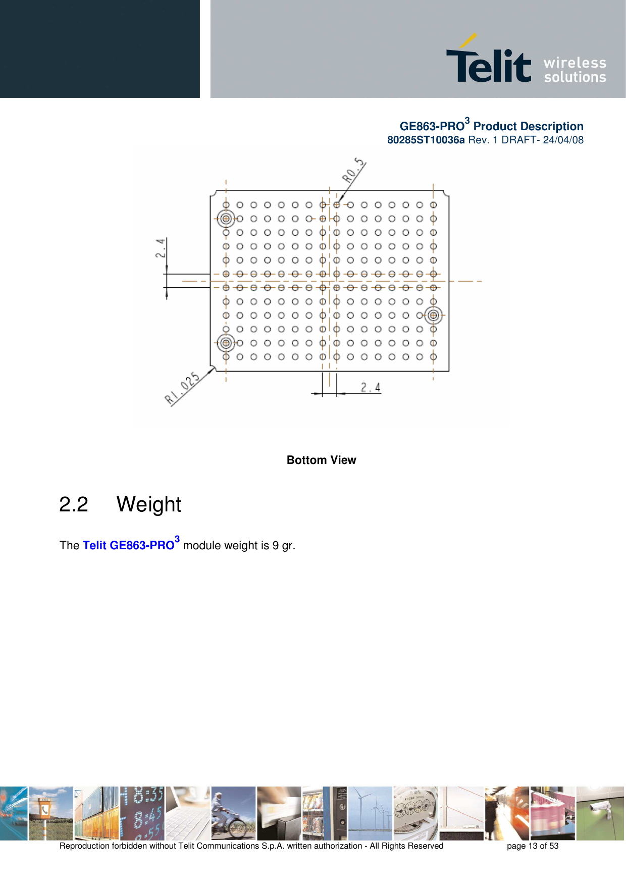
![GE863-PRO3 Product Description 80285ST10036a Rev. 1 DRAFT- 24/04/08 Reproduction forbidden without Telit Communications S.p.A. written authorization - All Rights Reserved page 11 of 53 2 General Product Description The Telit GE863-PRO3 module includes the GSM/GPRS engine plus a dedicated ARM9 application processor and memories. The two processors [GSM/GPRS engine & Application processor] are kept as much as possible distinct: they have different power sources but with the same voltage range, so that, either power management can be optimized, by splitting GSM and application supplies, or cost can be optimized, by using the same power source to supply the two parts. Furthermore in order to give the maximum flexibility the two engines can be operated independently each other. NOTE: The illustrations in this Product Description are only schematic and do not assure fidelity to construction or layout details, finishes, writings or colors. 2.1 Dimensions The Telit GE863-PRO3 module overall dimensions are: • Length: 41,4 mm • Width: 31,4 mm • Thickness: 3,6 mm The layout of the Telit GE863-PRO3 module is shown in the following figure:](https://usermanual.wiki/Telit-Communications-S-p-A/863P3/User-Guide-941147-Page-94.png)

![GE863-PRO3 Product Description 80285ST10036a Rev. 1 DRAFT- 24/04/08 Reproduction forbidden without Telit Communications S.p.A. written authorization - All Rights Reserved page 31 of 53 4 ARM9 Application Engine 4.1 General Description The Application engine is an ATMEL AT91SAM9260 and comprises an ARM926EJ-S processor with fast ROM and RAM plus power management and 8Mbyte SDRAM 100MHz and a 4Mbyte serial flash. The ARM926EJ-S has a full set of peripherals ranging from several USART to the USB Host controller, allowing almost any connectivity to be achieved. The ARM has two clock sources, a 6MHz crystal oscillator clock source providing the main clock that can be multiplied up to 200MHz and the internal RC slow clock source providing 32KHz. If more accuracy in the 32KHz clock is needed, then an external 32KHz crystal can be added. 4.2 Supply voltage The external power supply must be connected to VBATT2 signal pin (see Hardware User Guide) and must fulfill the following requirements: Nominal operating voltage 3.8 V Operating voltage range 3.4 V – 4.2 V Absolute Minimum voltage 3.30V Absolute Maximum voltage 4.50 V NOTE: Operating voltage range must never be exceeded; care must be taken in order to fulfill absolute min/max voltage requirements. 4.3 Power consumption The typical current consumption of the ARM9 part of the Telit GE863-PRO3 module is: Power off current (typical) < 1.5 µA Stand–by current @ slow clocking 1 mA [ TBD ] Operating current typical @ 200MHz 140 mA [ TBD ] The total power consumption of GE863-PRO3 is the sum of the consumptions of GSM and ARM9 processor part.](https://usermanual.wiki/Telit-Communications-S-p-A/863P3/User-Guide-941147-Page-114.png)
![GE863-PRO3 Product Description 80285ST10036a Rev. 1 DRAFT- 24/04/08 Reproduction forbidden without Telit Communications S.p.A. written authorization - All Rights Reserved page 32 of 53 4.4 USARTs The Application processor has 1 Full (9 wires) RS232 USART , 3 USART with Hardware Flow Control, 2 two wire UARTs. 4.5 SPI bus The Application processor has 2 set of Serial Peripheral Interfaces buses, SPI0 and SPI1. Each of these SPI bus has four Chip Select lines, that can be encoded to provide access to 15 peripherals [with external CS decoding]. The CS1 of the SPI0 bus is internally connected to the Serial Flash, hence SPI0 cannot use encoded CS and therefore only 3 other devices can be connected to the SPI0 interface. SPI1 bus can use the encoding. The SPI busses support Master, Multiple Master or Slave mode. The SPI bus consists of two data lines and two control lines: • Master Out Slave In (MOSI): This data line supplies the output data from the master shifted into the input(s) of the slave(s). • Master In Slave Out (MISO): This data line supplies the output data from a slave to the input of the master. There may be no more than one slave transmitting data during any particular transfer. • Serial Clock (SPCK): This control line is driven by the master and regulates the flow of the data bits. The master may transmit data at a variety of baud rates; the SPCK line cycles once for each bit that is transmitted. • Chip Select (NPCS): This control line allows slaves to be turned on and off by hardware. All combinations of Clock Polarity (CPOL) and Clock Phase (CPHA) is supported by the bus. 4.6 Image Sensor Interface The Image Sensor Interface (ISI) connects a CMOS-type image sensor to the processor and provides image capture in various formats. It does data conversion, if necessary, before the storage in memory through DMA. The ISI supports color CMOS image sensor and grayscale image sensors with a reduced set of functionalities. It supports two modes of synchronization: • Hardware with ISI_VSYNC and ISI_HSYNC signals • International Telecommunication Union Recommendation ITU-R BT.656-4 Startof-Active-Video (SAV) and End-of-Active-Video (EAV) synchronization sequence. Using EAV/SAV for synchronization reduces the pin count (ISI_VSYNC, ISI_HSYNC are not used). The polarity of the synchronization pulse is programmable to comply with the sensor signals.](https://usermanual.wiki/Telit-Communications-S-p-A/863P3/User-Guide-941147-Page-115.png)