Telit Communications S p A 863P3 Quad-Band GSM/GPRS module -Model: GE863-PRO3 User Manual Manual
Telit Communications S.p.A. Quad-Band GSM/GPRS module -Model: GE863-PRO3 Manual
Manual

GE863-PRO
3
Hardware User Guide
1vv0300773a Rev. 1 DRAFT - 24/04/08

GE863-PRO
3
Hardware User Guide
1vv0300773a Rev. 1 DRAFT -
24/04/08
Reproduction forbidden without Telit Communications S.p.A. written authorization - All Rights Reserved page 2 of 82
Contents
1 Overview ...........................................................................................................................7
2 GE863-PRO
3
Mechanical Dimensions ............................................................................8
3 GE863-PRO
3
module connections..................................................................................9
3.1
BALL-OUT............................................................................................................................. 9
3.2
BALLS LAYOUT .................................................................................................................. 15
3.3
ARM Port IO multiplexing..................................................................................................... 16
4 Hardware Commands ....................................................................................................19
4.1
Turning ON the GE863-PRO
3
GSM Engine ......................................................................... 19
4.2
Turning OFF the GE863-PRO
3
GSM Engine ....................................................................... 21
4.2.1
Hardware shutdown........................................................................................................................21
4.3
Hardware Unconditional Reboot of GSM Engine ................................................................. 21
4.4
Turning ON/OFF the GE863-PRO
3
ARM ............................................................................. 22
5 Power Supply..................................................................................................................24
5.1
GSM Power Supply Requirements....................................................................................... 24
5.2
ARM Power Supply Requirements....................................................................................... 25
5.3
VRTC Backup supply........................................................................................................... 25
5.4
General Design Rules.......................................................................................................... 26
5.4.1
Electrical design Guidelines............................................................................................................26
5.4.1.1
+ 5V input Source Power Supply Design Guidelines .................................................................27
5.4.1.2
+ 12V input Source Power Supply Design Guidelines ...............................................................28
5.4.1.3
Battery Source Power Supply Design Guidelines ......................................................................30
5.4.1.4
Battery Charge control Circuitry Design Guidelines ...................................................................30
5.4.2
Thermal Design Guidelines ............................................................................................................32
5.4.3
Power Supply PCB layout Guidelines ............................................................................................33
6 Antenna...........................................................................................................................34
6.1
GSM Antenna Requirements............................................................................................... 34
6.2
GSM Antenna - PCB line Guidelines.................................................................................... 35
6.3
GSM Antenna - installation Guidelines................................................................................. 36
6.4
Electro Magnetic Interference - Guidelines .......................................................................... 36
6.5
Logic level specifications ..................................................................................................... 37
6.5.1
GSM Reset signal...........................................................................................................................39
7 Serial Ports .....................................................................................................................40
7.1
MODEM SERIAL PORT ...................................................................................................... 40

GE863-PRO
3
Hardware User Guide
1vv0300773a Rev. 1 DRAFT -
24/04/08
Reproduction forbidden without Telit Communications S.p.A. written authorization - All Rights Reserved page 3 of 82
7.2
RS232 level translation........................................................................................................ 42
8 Audio Section Overview ................................................................................................45
8.1
Microphone Paths Characteristic and Requirements............................................................ 46
8.2
General Design Rules.......................................................................................................... 49
8.3
Other considerations............................................................................................................ 49
8.4
Microphone Biasing ............................................................................................................. 50
8.4.1
Balanced Microphone Biasing ........................................................................................................50
8.4.2
Unbalanced Microphone Biasing....................................................................................................51
8.5
Microphone Buffering........................................................................................................... 53
8.5.1
Buffered Balanced Mic....................................................................................................................53
8.5.2
Buffered Unbalanced (Single Ended) Microphone .........................................................................55
9 OUTPUT LINES (Speaker)..............................................................................................58
9.1
Short description.................................................................................................................. 58
9.2
Output Lines Characteristics................................................................................................ 59
9.3
General Design Rules.......................................................................................................... 60
9.3.1
Noise Filtering.................................................................................................................................60
9.4
Handset Earphone Design................................................................................................... 61
9.5
Hands-Free Earphone (Low Power) Design......................................................................... 62
9.6
Car Kit Speakerphone Design.............................................................................................. 63
9.7
The Evaluation Kit for Telit GE863-PRO
3
Modules............................................................... 64
9.7.1
Short Description ............................................................................................................................64
10 General Purpose I/O.......................................................................................................65
10.1
Using a GPIO Pad as INPUT ........................................................................................... 66
10.2
Using a GPIO Pad as OUTPUT........................................................................................ 66
10.3
Using the RF Transmission Control GPIO7...................................................................... 66
10.4
Using the RFTXMON Output GPIO3................................................................................ 66
10.5
Using the Alarm Output.................................................................................................... 67
10.6
Using the Buzzer Output GPIO4....................................................................................... 67
10.7
Indication of network service availability........................................................................... 68
10.8
RTC Bypass out............................................................................................................... 69
10.9
VAUX1 power output........................................................................................................ 69
11 Mounting the GE863-PRO
3
on the Application Board.................................................70
11.1
General ............................................................................................................................ 70
11.1.1
Recommended footprint for the application....................................................................................71
11.1.2
Stencil .............................................................................................................................................72
11.1.3
PCB pad Design .............................................................................................................................72
11.1.4
Solder paste....................................................................................................................................73

GE863-PRO
3
Hardware User Guide
1vv0300773a Rev. 1 DRAFT -
24/04/08
Reproduction forbidden without Telit Communications S.p.A. written authorization - All Rights Reserved page 4 of 82
11.1.5
GE863-PRO3 Solder Reflow ..........................................................................................................74
11.1.6
Packing System ..............................................................................................................................76
11.1.7
Moisture Sensibility.........................................................................................................................78
12 Conformity Assessment Issues....................................................................................79
13 SAFETY RECOMMANDATIONS.....................................................................................81
14 Document Change Log..................................................................................................82
GE863-PRO
3
Hardware User Guide
1vv0300773a Rev. 1 DRAFT -
24/04/08
Reproduction forbidden without Telit Communications S.p.A. written authorization - All Rights Reserved page 5 of 82
This document is relating to the following products:
GE863-PRO3 3990250691
GE863-PRO3 with Linux 3990250698

GE863-PRO
3
Hardware User Guide
1vv0300773a Rev. 1 DRAFT -
24/04/08
Reproduction forbidden without Telit Communications S.p.A. written authorization - All Rights Reserved page 6 of 82
DISCLAIMER
The information contained in this document is the proprietary information of Telit Communications
S.p.A. and its affiliates (“TELIT”). The contents are confidential and any disclosure to persons other
than the officers, employees, agents or subcontractors of the owner or licensee of this document,
without the prior written consent of Telit, is strictly prohibited.
Telit makes every effort to ensure the quality of the information it makes available. Notwithstanding the
foregoing, Telit does not make any warranty as to the information contained herein, and does not
accept any liability for any injury, loss or damage of any kind incurred by use of or reliance upon the
information.
Telit disclaims any and all responsibility for the application of the devices characterized in this
document, and notes that the application of the device must comply with the safety standards of the
applicable country, and where applicable, with the relevant wiring rules.
Telit reserves the right to make modifications, additions and deletions to this document due to
typographical errors, inaccurate information, or improvements to programs and/or equipment at any
time and without notice. Such changes will, nevertheless be incorporated into new editions of this
document.
All rights reserved.
© 2006 - 2008 Telit Communications S.p.A.
GE863-PRO
3
Hardware User Guide
1vv0300773a Rev. 1 DRAFT -
24/04/08
Reproduction forbidden without Telit Communications S.p.A. written authorization - All Rights Reserved page 7 of 82
1 Overview
The scope of this document is the description of some hardware solutions useful for developing a product with
the Telit
GE863-PRO
3
module.
In this document all the basic functions of a M2M device will be taken into account; for each one of them a
proper hardware solution will be suggested and eventually the wrong solutions and common errors to be
avoided will be evidenced. Obviously this document cannot embrace the whole hardware solutions and products
that may be designed. The wrong solutions to be avoided shall be considered as mandatory, while the
suggested hardware configurations shall not be considered mandatory, instead the information given shall be
used as a guide and a starting point for properly developing your product with the Telit
GE863-PRO
3
module. For
further hardware details that may not be explained in this document refer to the Telit GE863-PRO
3
Product
Description document.
NOTICE
(EN) The integration of the GSM/GPRS GE863-PRO
3
cellular module within user application shall be
done according to the design rules described in this manual.
(IT) L’integrazione del modulo cellulare GSM/GPRS GE863-PRO
3
all’interno dell’applicazione dell’utente
dovrà rispettare le indicazioni progettuali descritte in questo manuale.
(DE) Die integration des GE863-PRO
3
GSM/GPRS Mobilfunk-Moduls in ein Gerät muß gemäß der in
diesem Dokument beschriebenen Kunstruktionsregeln erfolgen
(SL) Integracija GSM/GPRS GE863-PRO
3
modula v uporabniški aplikaciji bo morala upoštevati projektna
navodila, opisana v tem piročniku.
(SP) La utilización del modulo GSM/GPRS GE863-PRO
3
debe ser conforme a los usos para los cuales ha
sido deseñado descritos en este manual del usuario.
(FR) L’intégration du module cellulaire GSM/GPRS GE863-PRO
3
dans l’application de l’utilisateur sera
faite selon les règles de conception décrites dans ce manuel.
The information presented in this document is believed to be accurate and reliable. However, no responsibility is
assumed by Telit Communications S.p.A. for its use, nor any infringement of patents or other rights of third
parties which may result from its use. No license is granted by implication or otherwise under any patent rights of
Telit Communications S.p.A. other than for circuitry embodied in Telit products. This document is subject to
change without notice.
GE863
-
PRO
3
GE863-PRO
3
Hardware User Guide
1vv0300773a Rev. 1 DRAFT -
24/04/08
Reproduction forbidden without Telit Communications S.p.A. written authorization - All Rights Reserved page 8 of 82
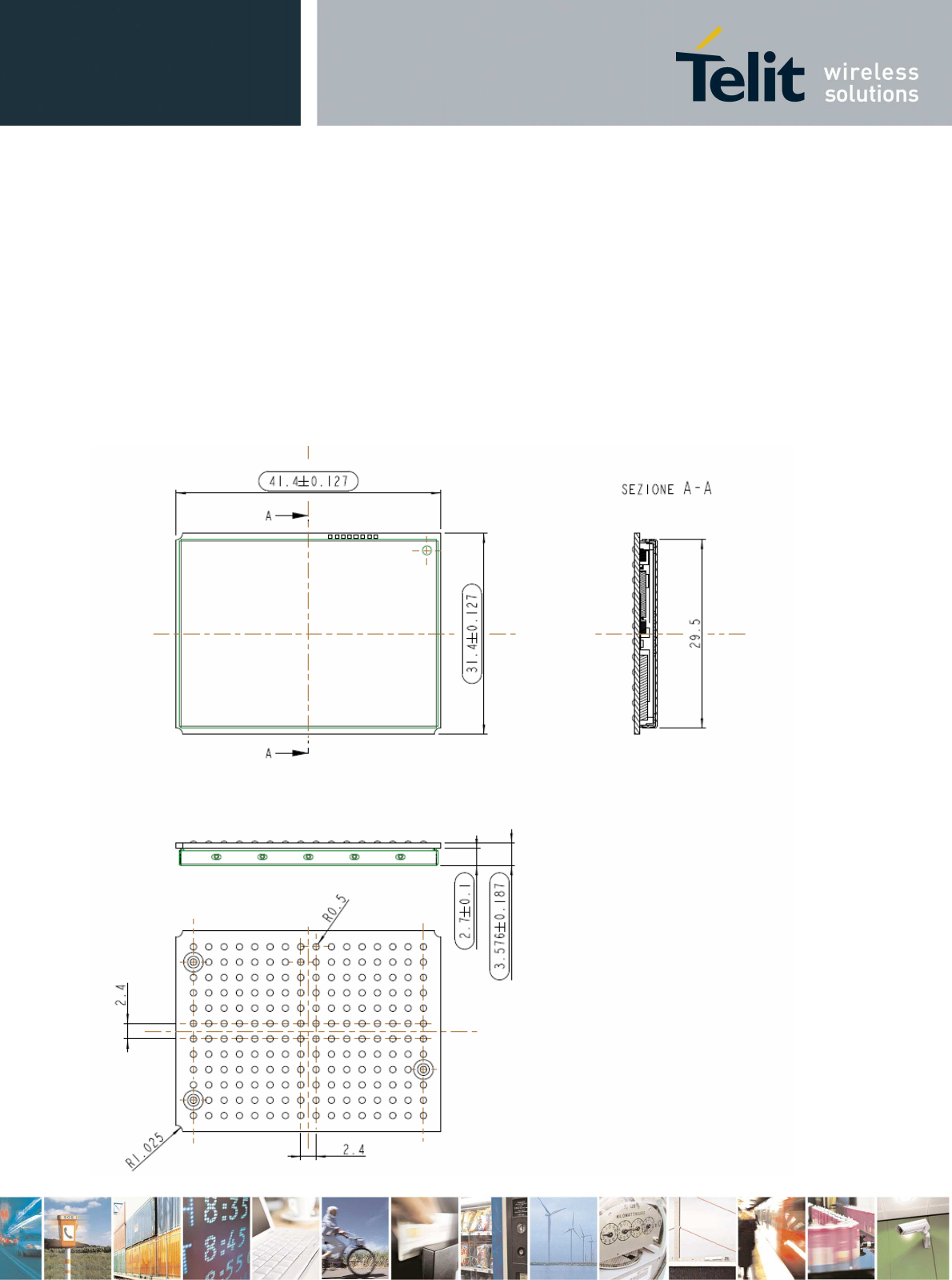
2 GE863-PRO3 Mechanical Dimensions
The Telit GE863-PRO
3
module overall dimension are:
• Length: 41,4 mm
• Width: 31,4 mm
• Thickness: 3,6 mm
GE863-PRO
3
Hardware User Guide
1vv0300773a Rev. 1 DRAFT -
24/04/08
Reproduction forbidden without Telit Communications S.p.A. written authorization - All Rights Reserved page 9 of 82
3 GE863-PRO3 module connections
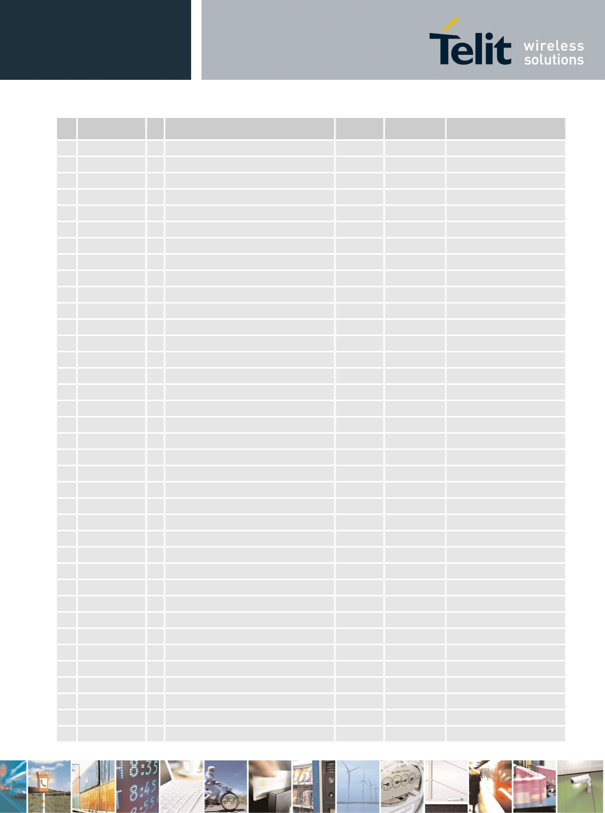
3.1 BALL-OUT
Ball
Signal I/O
Main Function Internal
Pull up ARM/ GSM Type
A1
RESERVED - RESERVED (3) - - -
A2
GND - Ground - - Power
A3
ANTENNA O
GSM Antenna output - 50 ohm - GSM RF
A4
RESERVED - RESERVED (3) - - -
A5
GND - Ground - - Power
A6
EAR_HF+ AO
Handsfree ear output, phase + GSM Audio
A7
EAR_HF- AO
Handsfree ear output, phase - GSM Audio
A8
EAR_MT+ AO
Handset earphone signal output, phase -
GSM Audio
A9
EAR_MT- AO
Handset earphone signal output, phase
+ GSM Audio
A10
TX_TRACE TX data for Debug (1) GSM CMOS 2.8V
A11
RX_TRACE RX data for Debug (1) CMOS 2.8V
A12
GND - Ground - - Power
B1
RESERVED - RESERVED (3) - - -
B2
GND - Ground - - Power
B3
GND - Ground - - Power
B4
GND - Ground - - Power
B5
GND - Ground - - Power
B6
MIC_HF+ AI
Handsfree microphone input; phase + GSM Audio
B7
MIC_HF- AI
Handsfree microphone input; phase - GSM Audio
B8
MIC_MT+ AI
Handset microphone signal input;
phase+ GSM Audio
B9
MIC_MT- AI
Handset microphone signal input; phase-
GSM Audio
B10
GPIO4 /
BUZZER I/O
GPIO4 / BUZZER output GSM CMOS 2.8V
B11
STAT_LED O
Status indicator led GSM CMOS 1.8V
B12
SIMIN I/O
External SIM signal - Presence (active
low) 47K
Ω
GSM CMOS 2.8V
C1
VBATT - Main GSM power supply GSM Power

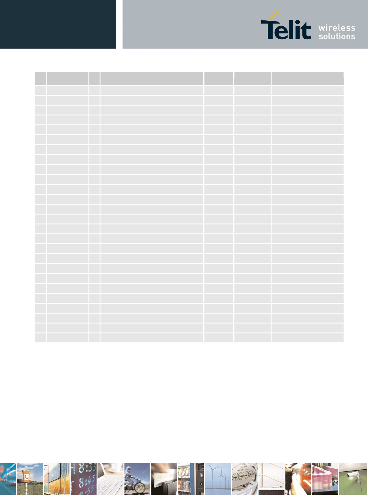
GE863-PRO
3
Hardware User Guide
1vv0300773a Rev. 1 DRAFT -
24/04/08
Reproduction forbidden without Telit Communications S.p.A. written authorization - All Rights Reserved page 10 of 82
Ball
Signal I/O
Main Function Internal
Pull up ARM/ GSM Type
C2
VBATT - Main GSM power supply GSM Power
C3
VRTC AO
VRTC Backup capacitor GSM-ARM Power
C4
C125/RING O
Output for Ring indicator signal (RI) to
DTE GSM CMOS 2.8V
C5
C107/DSR O
Output for Data set ready signal (DSR)
to DTE GSM CMOS 2.8V
C6
C108/DTR I Input for Data terminal ready signal
(DTR) from DTE GSM CMOS 2.8V
C7
C109/DCD O
Output for Data carrier detect signal
(DCD) to DTE GSM CMOS 2.8V
C8
C105/RTS I Input for Request to send signal (RTS)
from DTE GSM CMOS 2.8V
C9
C106/CTS O
Output for Clear to send signal (CTS) to
DTE GSM CMOS 2.8V
C10
GPIO7/
RFTXDISABLE
I/O
GPIO7 / RFTXDISABLE GSM CMOS 2.8V
C11
SIMRST O
External SIM signal – Reset GSM 1.8/3V ONLY
C12
SIMIO I/O
External SIM signal - Data I/O GSM 1.8/3V ONLY
D1
CHARGE AI
Charger input GSM Power
D2
VAUX1 - Power output for external accessories GSM -
D3
RESERVED - RESERVED (3) - - -
D4
PB25 I/O
ARM PIO Controller B pin 25 ARM CMOS 3.1V
D5
PB22
I/O
ARM PIO Controller B pin 22 ARM CMOS 3.1V
D6
PB24 I/O
ARM PIO Controller B pin 24 ARM CMOS 3.1V
D7
PB23 I/O
ARM PIO Controller B pin 23 ARM CMOS 3.1V
D8
PB26 I/O
ARM PIO Controller B pin 26 ARM CMOS 3.1V
D9
PB27 I/O
ARM PIO Controller B pin 27 ARM CMOS 3.1V
D10
GND - Ground - - Power
D11
SIMVCC - External SIM signal – Power (2) GSM 1.8/3V ONLY
D12
SIMCLK O
External SIM signal – Clock GSM 1.8/3V ONLY
E1
GND - Ground - - Power
E2
PWRMON O
Power ON Monitor GSM CMOS 2.8V
E3
RESERVED - RESERVED (3) - - -
E4
ON_OFF*-GSM
I Input command for switching power ON
or OFF to GSM Engine (toggle
command).
47K
Ω
GSM Pull up to VBATT
E5
RESET*-GSM
I GSM Engine Reset input GSM
E6
GPIO1 / JDR I/O
GPIO1
Configurable general purpose I/O
pin / Jammer Detect Output (2) GSM CMOS 2.8V
E7
GPIO5 I/O
GPIO5 Co
nfigurable general purpose I/O
pin GSM CMOS 2.8V
E8
GPIO3 /
RFTXMON I/O
GPIO3
Configurable general purpose I/O
pin / GSM CMOS 2.8V
E9
C103/TXD I Serial data input (TXD) from DTE GSM CMOS 2.8V

GE863-PRO
3
Hardware User Guide
1vv0300773a Rev. 1 DRAFT -
24/04/08
Reproduction forbidden without Telit Communications S.p.A. written authorization - All Rights Reserved page 11 of 82
Ball
Signal I/O
Main Function Internal
Pull up ARM/ GSM Type
E10
C104/RXD O
Serial data output to DTE GSM CMOS 2.8V
E11
PB8 I/O
ARM PIO Controller B pin 8 ARM CMOS 3.1V
E12
PB9 I/O
ARM PIO Controller B pin 9 ARM CMOS 3.1V
F1
PB13 I/O
ARM PIO Controller B pin 13 ARM CMOS 3.1V
F2
PC30 I/O
ARM PIO Controller C pin 30 ARM CMOS 1.8V-A
F3
PC21 I/O
ARM PIO Controller C pin 21 ARM CMOS 1.8V-A
F4
PC28 I/O
ARM PIO Controller C pin 28 ARM CMOS 1.8V-A
F5
PC29 I/O
ARM PIO Controller C pin 29 ARM CMOS 1.8V-A
F6
NRST I RESET ARM 1 K
Ω
ARM CMOS 3.1V
F7
ON/OFF*-AP I Input command for turning power ON or
OFF to ARM Engine (active high
command).
47K
Ω
ARM Pull up to VBATT2
F8
SHDN O
Shutdown Control Output ARM CMOS VRTC
F9
PB4 I/O
ARM PIO Controller B pin 4 ARM CMOS 3.1V
F10
PB5 I/O
ARM PIO Controller B pin 5 ARM CMOS 3.1V
F11
PC8 I/O
ARM PIO Controller C pin 8 ARM CMOS 1.8V-A
F12
PC10 I/O
ARM PIO Controller C pin 10 ARM CMOS 1.8V-A
G1
PB12 I/O
ARM PIO Controller B pin 12 ARM CMOS 3.1V
G2
RESERVED - RESERVED (3) - - -
G3
PC31 I/O
ARM PIO Controller C pin 31 ARM CMOS 1.8V-A
G4
GPIO2 /
PCMCLK I/O
GPIO2 Configura
ble general purpose I/O
pin 4.7K
Ω
GSM CMOS 2.8V
G5
GPIO8 /
PCMWAO I/O
GPIO8
Configurable general purpose I/O
pin GSM CMOS 2.8V
G6
GPIO6 /
PCMTX I/O
GPIO6
Configurable general purpose I/O
pin GSM CMOS 2.8V
G7
GPIO9 –
PCMRX I/O
GPIO9 Configurable gener
al purpose I/O
pin GSM CMOS 2.8V
G8
RESERVED - RESERVED (3) - - -
G9
PA5 I/O
ARM PIO Controller A pin 5 ARM CMOS 3.1V
G10
PA4 I/O
ARM PIO Controller A pin 4 ARM CMOS 3.1V
G11
PB10 I/O
ARM PIO Controller B pin 10 ARM CMOS 3.1V
G12
PB11 I/O
ARM PIO Controller B pin 11 ARM CMOS 3.1V
H1
PB6 I/O
ARM PIO Controller B pin 6 ARM CMOS 3.1V
H2
PB29 I/O
ARM PIO Controller B pin 29 ARM CMOS 3.1V
H3
GND - Ground - - Power
H4
PB20 I/O
ARM PIO Controller B pin 20 ARM CMOS 3.1V
H5
PB21 I/O
ARM PIO Controller B pin 21 ARM CMOS 3.1V
H6
PB19 I/O
ARM PIO Controller B pin 19 ARM CMOS 3.1V
H7
PB18 I/O
ARM PIO Controller B pin 18 ARM CMOS 3.1V
H8
RESERVED - RESERVED (3) - - -
GE863-PRO
3
Hardware User Guide
1vv0300773a Rev. 1 DRAFT -
24/04/08
Reproduction forbidden without Telit Communications S.p.A. written authorization - All Rights Reserved page 12 of 82
Ball
Signal I/O
Main Function Internal
Pull up ARM/ GSM Type
H9
PC18 I/O
ARM PIO Controller C pin 18 ARM CMOS 1.8V-A
H10
PB0 I/O
ARM PIO Controller B pin 0 ARM CMOS 3.1V
H11
PB2 I/O
ARM PIO Controller B pin 2 ARM CMOS 3.1V
H12
PB1 I/O
ARM PIO Controller B pin 1 ARM CMOS 3.1V
J1
PB7 I/O
ARM PIO Controller B pin 7 ARM CMOS 3.1V
J2
PB28 I/O
ARM PIO Controller B pin 28 ARM CMOS 3.1V
J3
RESERVED - RESERVED (3) - - -
J4
PB16 I/O
ARM PIO Controller B pin 16 ARM CMOS 3.1V
J5
PB17 I/O
ARM PIO Controller B pin 17 ARM CMOS 3.1V
J6
PC15 I/O
ARM PIO Controller C pin 15 ARM CMOS 1.8V-A
J7
PC14 I/O
ARM PIO Controller C pin 14 ARM CMOS 1.8V-A
J8
RESERVED - RESERVED (3) - - -
J9
PC4 I/O
ARM PIO Controller C pin 4 ARM CMOS 1.8V-A
J10
PC5 I/O
ARM PIO Controller C pin 5 ARM CMOS 1.8V-A
J11
PC19 I/O
ARM PIO Controller C pin 19 ARM CMOS 1.8V-A
J12
PC20 I/O
ARM PIO Controller C pin 20 ARM CMOS 1.8V-A
K1
PA23 I/O
ARM PIO Controller A pin 23 ARM CMOS 3.1V
K2
PA29 I/O
ARM PIO Controller A pin 29 ARM CMOS 3.1V
K3
TMS I JTAG ARM - Test Mode Select Pull Down
ARM CMOS 3.1V
K4
TCK I JTAG ARM – Test Clock ARM CMOS 3.1V
K5
RTCK O
JTAG ARM – Returned Test Clock ARM CMOS 3.1V
K6
PA25 I/O
ARM PIO Controller A pin 25 ARM CMOS 3.1V
K7
PC13 I/O
ARM PIO Controller C pin 13 ARM CMOS 1.8V-A
K8
PC6 I/O
ARM PIO Controller C pin 6 ARM CMOS 1.8V-A
K9
PC7 I/O
ARM PIO Controller C pin 7 ARM CMOS 1.8V-A
K10
PB3 I/O
ARM PIO Controller B pin 3 ARM CMOS 3.1V
K11
HDMA A USB Host Port A Data - ARM USB
K12
HDPA A USB Host Port A Data + ARM USB
L1
PA24 I/O
ARM PIO Controller A pin 24 ARM CMOS 3.1V
L2
OSCSEL I Slow Clock Oscillator Selection Pull Down
ARM CMOS VRTC
L3
NTRST I JTAG ARM - Test Reset Pull Up ARM CMOS 3.1V
L4
TDI I JTAG ARM - Test Data Input ARM CMOS 3.1V
L5
TDO O
JTAG ARM - Test Data Output ARM CMOS 3.1V
L6
JTAGSEL I JTAG ARM – JTAG Type Selection Pull Down
ARM CMOS 3.1V
L7
PA28 I/O
ARM PIO Controller A pin 28 ARM CMOS 3.1V
L8
PA27 I/O
ARM PIO Controller A pin 27 ARM CMOS 3.1V
L9
PA26 I/O
ARM PIO Controller A pin 26 ARM CMOS 3.1V

GE863-PRO
3
Hardware User Guide
1vv0300773a Rev. 1 DRAFT -
24/04/08
Reproduction forbidden without Telit Communications S.p.A. written authorization - All Rights Reserved page 13 of 82
Ball
Signal I/O
Main Function Internal
Pull up ARM/ GSM Type
L10
GND - Ground - - Power
L11
HDMB A USB Host Port B Data - ARM USB
L12
HDPB A USB Host Port B Data + ARM USB
M1
XIN32 I Slow Clock Oscillator Input ARM CMOS VRTC
M2
XOUT32 O
Slow Clock Oscillator Output ARM CMOS VRTC
M3
RESERVED - RESERVED (3) - - -
M4
RESERVED - RESERVED (3) - - -
M5
PB14 I/O
ARM PIO Controller B pin 14 ARM CMOS 3.1V
M6
PB15 I/O
ARM PIO Controller B pin 15 ARM CMOS 3.1V
M7
PC22 I/O
ARM PIO Controller C pin 22 ARM CMOS 1.8V-A
M8
PC9 I/O
ARM PIO Controller C pin 9 ARM CMOS 1.8V-A
M9
PA3 I/O
ARM PIO Controller A pin 3 ARM CMOS 3.1V
M10
PA2 I/O
ARM PIO Controller A pin 2 ARM CMOS 3.1V
M11
PA1 I/O
ARM PIO Controller A pin 1 ARM CMOS 3.1V
M12
PA0 I/O
ARM PIO Controller A pin 0 ARM CMOS 3.1V
N1
PA11 I/O
ARM PIO Controller A pin 11 ARM CMOS 3.1V
N2
PA10 I/O
ARM PIO Controller A pin 10 ARM CMOS 3.1V
N3
PA9 I/O
ARM PIO Controller A pin 9 ARM CMOS 3.1V
N4
PA31 I/O
ARM PIO Controller A pin 31 ARM CMOS 3.1V
N5
PA30 I/O
ARM PIO Controller A pin 30 ARM CMOS 3.1V
N6
PB31 I/O
ARM PIO Controller B pin 31 ARM CMOS 3.1V
N7
GND - Ground - - Power
N8
PC16 I/O
ARM PIO Controller C pin 16 ARM CMOS 1.8V-A
N9
PC17 I/O
ARM PIO Controller C pin 17 ARM CMOS 1.8V-A
N10
RESERVED - RESERVED (3) - - -
N11
DDM A USB Device Port Data - ARM USB
N12
DDP A USB Device Port Data + ARM USB
P1
PA6 I/O
ARM PIO Controller A pin 6 ARM CMOS 3.1V
P2
PA7 I/O
ARM PIO Controller A pin 7 ARM CMOS 3.1V
P3
PA8 I/O
ARM PIO Controller A pin 8 ARM CMOS 3.1V
P4
PC12 I/O
ARM PIO Controller C pin 12 ARM CMOS 1.8V-A
P5
PB30 I/O
ARM PIO Controller B pin 30 ARM CMOS 3.1V
P6
PC0 I/O
ARM PIO Controller C pin 0 ARM CMOS 3.1V
P7
PC1 I/O
ARM PIO Controller C pin 1 ARM CMOS 3.1V
P8
PC2 I/O
ARM PIO Controller C pin 2 ARM CMOS 3.1V
P9
PC3 I/O
ARM PIO Controller C pin 3 ARM CMOS 3.1V
P10
PA22 I/O
ARM PIO Controller A pin 22 ARM CMOS 3.1V
GE863-PRO
3
Hardware User Guide
1vv0300773a Rev. 1 DRAFT -
24/04/08
Reproduction forbidden without Telit Communications S.p.A. written authorization - All Rights Reserved page 14 of 82
Ball
Signal I/O
Main Function Internal
Pull up ARM/ GSM Type
P11
3.1V_OUT OA
ARM 3.1V Power Output ARM -
P12
VBATT2 - Main ARM Power Supply ARM Power
R1
GND - Ground - - Power
R2
GND - Ground - - Power
R3
GND - Ground - - Power
R4
PA21 I/O
ARM PIO Controller A pin 21 ARM CMOS 3.1V
R5
PA18 I/O
ARM PIO Controller A pin 18 ARM CMOS 3.1V
R6
PA17 I/O
ARM PIO Controller A pin 17 ARM CMOS 3.1V
R7
PA19 I/O
ARM PIO Controller A pin 19 ARM CMOS 3.1V
R8
PA16 I/O
ARM PIO Controller A pin 16 ARM CMOS 3.1V
R9
RESERVED - RESERVED (3) - - -
R10
GND - Ground - - Power
R11
GND - Ground - - Power
R12
GND - Ground - - Power
S1
RESERVED - RESERVED (3) - - -
S2
RESERVED - RESERVED (3) - - -
S3
GND - Ground - - Power
S4
PA20 I/O
ARM PIO Controller A pin 20 ARM CMOS 3.1V
S5
PA14 I/O
ARM PIO Controller A pin 14 ARM CMOS 3.1V
S6
PA15 I/O
ARM PIO Controller A pin 15 ARM CMOS 3.1V
S7
PA12 I/O
ARM PIO Controller A pin 12 ARM CMOS 3.1V
S8
PA13 I/O
ARM PIO Controller A pin 13 ARM CMOS 3.1V
S9
RESERVED - RESERVED (3) - - -
S10
GND - Ground - - Power
S11
RESERVED - RESERVED (3) - - -
S12
RESERVED - RESERVED (3) - - -
(1) For the exclusive use of the Technical Support Service
(2) On this pin a maximum of 10nF bypass capacitor is allowed.
(3) Reserved Pins must be left UNCONNECTED
GE863-PRO
3
Hardware User Guide
1vv0300773a Rev. 1 DRAFT -
24/04/08
Reproduction forbidden without Telit Communications S.p.A. written authorization - All Rights Reserved page 15 of 82
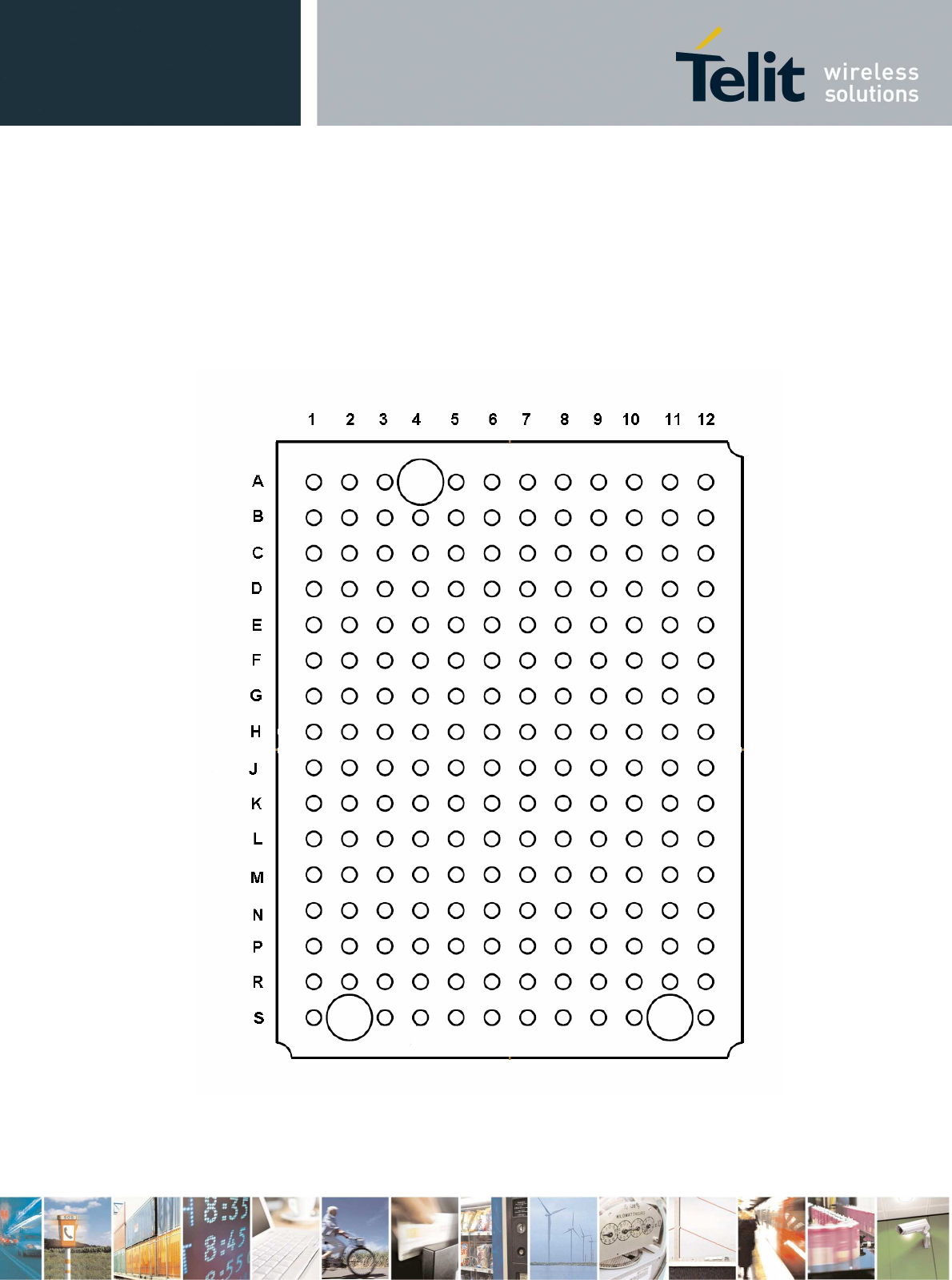
3.2 BALLS LAYOUT
TOP VIEW
GE863-PRO
3
Hardware User Guide
1vv0300773a Rev. 1 DRAFT -
24/04/08
Reproduction forbidden without Telit Communications S.p.A. written authorization - All Rights Reserved page 16 of 82
3.3 ARM Port IO multiplexing
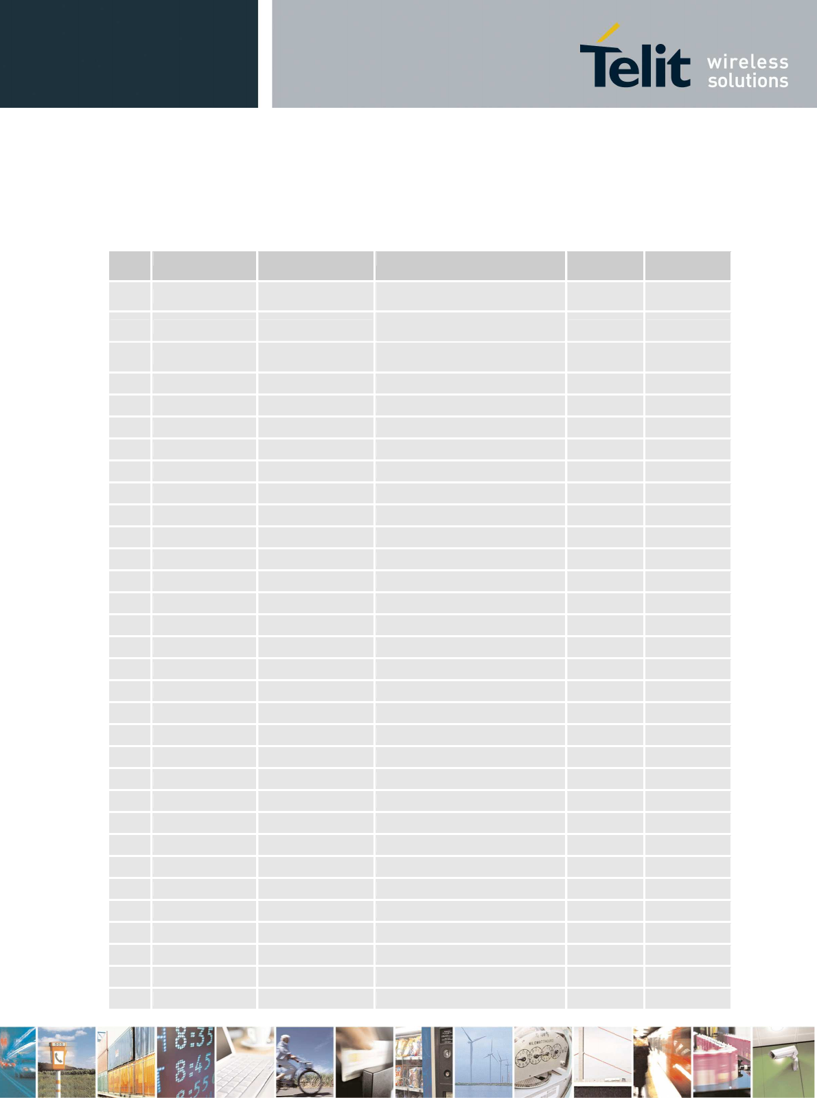
ARM PIO Controller A multiplexing
IO
linel Peripheral A Peripheral B Comments Reset State
Boot State
PA0 SPI0_MISO MCDB0 Connected to internal dataflash
SO (1) I/O SPI0_MISO
PA1 SPI0_MOSI MCCDB
Connected to internal dataflash SI
(1) I/O SPI0_MOSI
PA2 SPI0_SPCK Connected to internal dataflash
CLK (1) I/O SPI0_SPCK
PA3 SPI0_NPCS0 MCDB3 I/O SPI0_NPCS0
PA4 RTS2 MCDB2 I/O I with Pull-up
PA5 CTS2 MCDB1 I/O I with Pull-up
PA6 MCDA0 I/O I with Pull-up
PA7 MCCDA I/O I with Pull-up
PA8 MCCK I/O I with Pull-up
PA9 MCDA1 I/O I with Pull-up
PA10
MCDA2 ETX2 I/O I with Pull-up
PA11
MCDA3 ETX3 I/O I with Pull-up
PA12
ETX0 I/O I with Pull-up
PA13
ETX1 I/O I with Pull-up
PA14
ERX0 I/O I with Pull-up
PA15
ERX1 I/O I with Pull-up
PA16
ETXEN I/O I with Pull-up
PA17
ERXDV I/O I with Pull-up
PA18
ERXER I/O I with Pull-up
PA19
ETXCK I/O I with Pull-up
PA20
EMDC I/O I with Pull-up
PA21
EMDIO I/O I with Pull-up
PA22
ADTRG ETXER I/O I with Pull-up
PA23
TWD ETX2 I/O I with Pull-up
PA24
TWCK ETX3 I/O I with Pull-up
PA25
TCLK0 ERX2 I/O I with Pull-up
PA26
TIOA0 ERX3 I/O I with Pull-up
PA27
TIOA1 ERXCK I/O I with Pull-up
PA28
TIOA2 ECRS I/O I with Pull-up
PA29
SCK1 ECOL I/O I with Pull-up
PA30
SCK2 RXD4 I/O I with Pull-up
PA31
SCK0 TXD4 I/O I with Pull-up
GE863-PRO
3
Hardware User Guide
1vv0300773a Rev. 1 DRAFT -
24/04/08
Reproduction forbidden without Telit Communications S.p.A. written authorization - All Rights Reserved page 17 of 82
ARM PIO Controller B multiplexing
IO
linel Peripheral A Peripheral B Comments Reset State
Boot State
PB0 SPI1_MISO TIOA3 I/O I with Pull-up
PB1 SPI1_MOSI TIOB3 I/O I with Pull-up
PB2 SPI1_SPCK TIOA4 I/O I with Pull-up
PB3 SPI1_NPCS0 TIOA5 I/O I with Pull-up
PB4 TXD0 I/O I with Pull-up
PB5 RXD0 I/O I with Pull-up
PB6 TXD1 TCLK1 I/O I with Pull-up
PB7 RXD1 TCLK2 I/O I with Pull-up
PB8 TXD2 I/O I with Pull-up
PB9 RXD2 I/O I with Pull-up
PB10
TXD3 ISI_D8 I/O I with Pull-up
PB11
RXD3 ISI_D9 I/O I with Pull-up
PB12
TXD5 ISI_D10 I/O I with Pull-up
PB13
RXD5 ISI_D11 I/O I with Pull-up
PB14
DRXD I/O I with Pull-up
PB15
DTXD I/O I with Pull-up
PB16
TK0 TCLK3 I/O I with Pull-up
PB17
TF0 TCLK4 I/O I with Pull-up
PB18
TD0 TIOB4 I/O I with Pull-up
PB19
RD0 TIOB5 I/O I with Pull-up
PB20
RK0 ISI_D0 I/O I with Pull-up
PB21
RF0 ISI_D1 I/O I with Pull-up
PB22
DSR0 ISI_D2 I/O I with Pull-up
PB23
DCD0 ISI_D3 I/O I with Pull-up
PB24
DTR0 ISI_D4 I/O I with Pull-up
PB25
RI0 ISI_D5 I/O I with Pull-up
PB26
RTS0 ISI_D6 I/O I with Pull-up
PB27
CTS0 ISI_D7 I/O I with Pull-up
PB28
RTS1 ISI_PCK I/O I with Pull-up
PB29
CTS1 ISI_VSYNC I/O I with Pull-up
PB30
PCK0 ISI_HSYNC I/O I with Pull-up
PB31
PCK1 ISI_MCK I/O I with Pull-up

GE863-PRO
3
Hardware User Guide
1vv0300773a Rev. 1 DRAFT -
24/04/08
Reproduction forbidden without Telit Communications S.p.A. written authorization - All Rights Reserved page 18 of 82
ARM PIO Controller C multiplexing
IO
linel Peripheral A Peripheral B Comments Reset State
Boot State
PC0 SCK3 AD0 I/O I with Pull-up
PC1 PCK0 AD1 I/O I with Pull-up
PC2 PCK1 AD2 I/O I with Pull-up
PC3 SPI1_NPCS3 AD3 I/O I with Pull-up
PC4 A23 SPI1_NPCS2 A23 I with Pull-up
PC5 A24 SPI1_NPCS1 A24 I with Pull-up
PC6 TIOB2 CFCE1 I/O I with Pull-up
PC7 TIOB1 CFCE2 I/O I with Pull-up
PC8 NCS4/CFCS0 RTS3 I/O I with Pull-up
PC9 NCS5/CFCS1 TIOB0 I/O I with Pull-up
PC10
A25/CFRNW CTS3 A25 I with Pull-up
PC11
NCS2 SPI0_NPCS1 Connected to internal dataflash
CS line
NOT AVAILABLE on the Balls I/O SPI0_NPCS1
PC12
IRQ0 NCS7 I/O I with Pull-up
PC13
FIQ NCS6 I/O I with Pull-up
PC14
NCS3/NANDCS IRQ2 I/O I with Pull-up
PC15
NWAIT IRQ1 I/O I with Pull-up
PC16
D16 SPI0_NPCS2 I/O SPI0_NPCS2
with pull-up
PC17
D17 SPI0_NPCS3 I/O SPI0_NPCS3
with pull-up
PC18
D18 SPI1_NPCS1 I/O I with Pull-up
PC19
D19 SPI1_NPCS2 I/O I with Pull-up
PC20
D20 SPI1_NPCS3 I/O I with Pull-up
PC21
D21 EF100 I/O I with Pull-up
PC22
D22 TCLK5 I/O I with Pull-up
PC23
D23 Enable of 6MHz internal ARM
Oscillator (active High)
NOT AVAILABLE on the Balls I/O O HIGH
PC24
D24 NOT AVAILABLE on the Balls I/O -
PC25
D25 NOT AVAILABLE on the Balls I/O -
PC26
D26 NOT AVAILABLE on the Balls I/O -
PC27
D27 NOT AVAILABLE on the Balls I/O -
PC28
D28 I/O I with Pull-up
PC29
D29
GPIO that rises to keep externally
ARM alive I/O O HIGH
PC30
D30 I/O I with Pull-up
PC31
D31 I/O I with Pull-up

GE863-PRO
3
Hardware User Guide
1vv0300773a Rev. 1 DRAFT -
24/04/08
Reproduction forbidden without Telit Communications S.p.A. written authorization - All Rights Reserved page 19 of 82
TIP: For further documentation on ARM processor refer to ATMEL AT91SAM9260 datasheet
4 Hardware Commands
4.1 Turning ON the GE863-PRO
3
GSM Engine
To turn on the GE863-PRO
3
GSM/GPRS engine the pad
ON_OFF*-GSM
must be tied low for at least 1
second and then released.
The maximum current that can be drained from the
ON_OFF*-GSM
pad is 0,1 mA.
A simple circuit to do it is:
NOTE: don't use any pull up resistor on the ON# line, it is internally pulled up. Using pull up resistor may
bring to latch up problems on the GE863-PRO3 power regulator and improper power on/off of the module.
The line ON# must be connected only in open collector configuration.
NOTE: In this document all the lines that are inverted, hence have active low signals are labeled with a
name that ends with a "*" or with a bar over the name.
NOTE: The GE863-PRO3 turns fully on also by supplying power to the Charge pad (Module provided with a battery
on the VBATT pads).
TIP: To check if the device has powered on, the hardware line PWRMON should be monitored. After 900ms the line
raised up the device could be considered powered on.
PWRMON line rises up also when supplying power to the Charge pad
ON#
Power ON impulse
GND
R1
R2
Q1

GE863-PRO
3
Hardware User Guide
1vv0300773a Rev. 1 DRAFT -
24/04/08
Reproduction forbidden without Telit Communications S.p.A. written authorization - All Rights Reserved page 20 of 82
For example:
1- Let's assume you need to drive the ON_OFF*-GSM pad with a totem pole output of a +3/5 V
microcontroller (uP_OUT1):
2- Let's assume you need to drive the ON_OFF*-GSM pad directly with an ON/OFF button:
1s
10k

GE863-PRO
3
Hardware User Guide
1vv0300773a Rev. 1 DRAFT -
24/04/08
Reproduction forbidden without Telit Communications S.p.A. written authorization - All Rights Reserved page 21 of 82
4.2 Turning OFF the GE863-PRO
3
GSM Engine
The turning off of the device can be done in two ways:
• by software command (see GE863- GE863-PRO
3
Software User Guide)
• by hardware shutdown
When the device is shut down by software command or by hardware shutdown, it issues to the
network a detach request that informs the network that the device will not be reachable any more.
4.2.1 Hardware shutdown
To turn OFF the GE863-PRO
3
the pad ON_OFF*-GSM must be tied low for at least 1 second and
then released.
The same circuitry and timing for the power on shall be used.
The device shuts down after the release of the ON_OFF*-GSM pad.
TIP: To check if the device has powered off, the hardware line PWRMON should be monitored. When
PWRMON goes low, the device has powered off.
4.3 Hardware Unconditional Reboot of GSM Engine
To unconditionally Reboot the GE863-PRO3 , the pad RESET*-GSM must be tied low for at least 200
milliseconds and then released.
The maximum current that can be drained from the RESET*-GSM pad is 0,15 mA.
A simple circuit to do it is:
RESET*-GSM
Unconditional Reboot
impulse
GND

GE863-PRO
3
Hardware User Guide
1vv0300773a Rev. 1 DRAFT -
24/04/08
Reproduction forbidden without Telit Communications S.p.A. written authorization - All Rights Reserved page 22 of 82
NOTE: don't use any pull up resistor on the RESET*-GSM line nor any totem pole digital output. Using pull
up resistor may bring to latch up problems on the GE863-PRO3 power regulator and improper functioning
of the module. The line RESET*-GSM must be connected only in open collector configuration.
TIP: The unconditional hardware reboot should be always implemented on the boards and software
should use it as an emergency exit procedure.
For example:
1- Let's assume you need to drive the RESET*-GSM ( RESET ) pad with a totem pole output of a +3/5
V microcontroller (uP_OUT2):
4.4 Turning ON/OFF the GE863-PRO
3
ARM
To turn on the GE863-PRO
3
ARM the pad
ON_OFF*-ARM
must be tied low and kept low, when pin is
raised ( released ) the ARM will shutdown.
The maximum current that can be drained from the
ON_OFF*-ARM
pad is 0,1 mA.
A simple circuit to do it is:
10k

GE863-PRO
3
Hardware User Guide
1vv0300773a Rev. 1 DRAFT -
24/04/08
Reproduction forbidden without Telit Communications S.p.A. written authorization - All Rights Reserved page 23 of 82
NOTE: don't use any pull up resistor on the ON/OFF*ARM line, it is internally pulled up to VBATT2. Using
pull up resistor may bring to latch up problems on the GE863-PRO
3
power regulator and improper power
on/off of the module. The line ON/OFF*-ARM must be connected only in open collector configuration or
tied to ground (if ARM needs to stay always on).
NOTE: In this document all the lines that are inverted, hence have active low signals are labeled with a
name that ends with a "*" or with a bar over the name.
TIP: To check if the device has powered on, the hardware line 3.1V_OUT can be monitored.
It is possible to use also the SHDN line to turn ON the device with the ARM RTC trigger by connecting
it to the ON/OFF*-ARM pin through a transistor buffer.
After the Initial bootstrap, the line PC29 goes HIGH allowing the device to keep itself on;
If you need a toggle command to turn on/off the device, then you can use the line PC29 to keep the
ARM on after it’s start-up and connect the on/off button to the ON/OFF*ARM pin through a buffer
transistor while connecting it to a GPIO to sense it’s toggling (e.g. PC31) for shutting down the ARM
by lowering the PC29 pin.
TIP: To Keep the ARM ON you can use the PC29 pin that goes high right after the bootstrap
ON/OFF*-ARM#
Power ON/OFF
GND
R1
R2
Q1
GE863-PRO
3
Hardware User Guide
1vv0300773a Rev. 1 DRAFT -
24/04/08
Reproduction forbidden without Telit Communications S.p.A. written authorization - All Rights Reserved page 24 of 82
5 Power Supply
The power supply circuitry and board layout are a very important part in the full product design and
they strongly reflect on the product overall performances, hence read carefully the requirements and
the guidelines that will follow for a proper design.
In the GE863-PRO
3
the power supply inputs of the GSM engine and the ARM processor part have
been kept separate, VBATT is the input for the GSM part, VBATT2 is the input for ARM.
It is possible to connect together the two power inputs since they have compatible ranges, but if it is
desired the two power supplies can be kept separate.
The only power supply in common between the ARM and GSM engine is the RTC voltage which is
generated by the GSM engine from VBATT power source and supplies both the GSM RTC and the
ARM VDDBU part including the shutdown controller, rtc, 32 KHz oscillator. For this reason if it is
planned to remove VBATT power supply, then a backup battery shall be provided on VTRC pin that
guarantees that VRTC is still available.
NOTE: if you plan to remove VBATT power source, then you must provide an appropriate backup
battery/capacitor on the VRTC pin in order to be able to turn on properly the ARM part when supplying
VBATT2 only power pin.
5.1 GSM Power Supply Requirements
POWER SUPPLY
Nominal Supply Voltage 3.8 V
Max Supply Voltage 4.2 V
Supply voltage range 3.4 V - 4.2 V
GE863-PRO3 GSM Engine
Mode Average (mA) Mode description
IDLE mode Stand by mode; no call in progress
AT+CFUN=1 24,0 Normal mode: full functionality of the module
AT+CFUN=4 22,0 Disabled TX and RX; module is not registered on the network
AT+CFUN=0 or
AT+CFUN=5 7,20 / 3,56
1
Power saving: CFUN=0 module registered on the network and can
receive voice call or an SMS; but it is not possible to send AT
commands; module wakes up with an unsolicited code (call or
SMS) or rising RTS line. CFUN=5 full functionality with power
saving; module registered on the network can receive incoming
calls and SMS
RX mode
1 slot in downlink 53,0
2 slot in downlink 66,0
3 slot in downlink 79,0
4 slot in downlink 89,0
GSM Receiving data mode
1
Worst/best case depends on network configuration and is not under module control
GE863-PRO
3
Hardware User Guide
1vv0300773a Rev. 1 DRAFT -
24/04/08
Reproduction forbidden without Telit Communications S.p.A. written authorization - All Rights Reserved page 25 of 82
GSM TX and RX mode
Min power level 78,0
Max power level 200,0
GSM Sending data mode
GPRS (class 10) TX and RX mode
Min power level 124,0
Max power level 371,0
GPRS Sending data mode
The GSM system is made in a way that the RF transmission is not continuous, else it is packed into
bursts at a base frequency of about 216 Hz, the relative current peaks can be as high as about 2A.
Therefore the power supply has to be designed in order to withstand with these current peaks without
big voltage drops; this means that both the electrical design and the board layout must be designed for
this current flow. If the layout of the PCB is not well designed a strong noise floor is generated on the
ground and the supply; this will reflect on all the audio paths producing an audible annoying noise at
216 Hz; if the voltage drop during the peak current absorption is too much, then the device may even
shutdown as a consequence of the supply voltage drop.
TIP: The electrical design for the Power supply should be made ensuring it will be capable of a peak
current output of at least 2 A.
5.2 ARM Power Supply Requirements
POWER SUPPLY
Nominal Supply Voltage 3.8 V
Operating Supply voltage range 3.4 V - 4.2 V
Absolute Maximum voltage range 3.30 – 4.5 V
GE863-PRO3
Mode Typical Average (mA) Mode description
Off < 2 µA (TBD)
Full Speed 140 (TBD) ARM is operational at full speed 200MHz CPU Clock , Main Clock
100 MHz and all peripherals active
Slow Clocking 1 (TBD) ARM is running on slow clock with peripherals disabled
5.3 VRTC Backup supply
The RTC of the GPRS Engine and the RTC & Shutdown controller of the ARM part are supplied by
VRTC. This voltage supply is generated by a low quiescent current regulator inside the module that
takes its power from VBATT pins. Since this voltage supply is needed to correctly boot the ARM part,
if it is planned to remove the VBATT supply and still turn on the ARM part supplied by VBATT2, then
an appropriate power supply must be provided to the VRTC pin.
To obtain several working years for the Real Time Clock of the GPRS engine and the RTC, 32KHz
oscillator & Shutdown controller of the ARM part without VBATT power supply voltage, it is needed to
make use of a lithium primary battery to supply the RTC circuits in the Telit Module.
The operative voltage for VRTC is lower than the voltage of primary lithium battery (3V nominal).
It is therefore necessary to put a LDO voltage regulator in the circuit.

GE863-PRO
3
Hardware User Guide
1vv0300773a Rev. 1 DRAFT -
24/04/08
Reproduction forbidden without Telit Communications S.p.A. written authorization - All Rights Reserved page 26 of 82
The suggested circuit is:
The quoted current intensity are without VBATT power supply for the module.
The S-817A19A
Seiko LDO has a value of 1.2µ
µµ
µA Typ for the quiescent current. Without VBATT power
supply voltage, the VRTC Reverse Current is 7- 8 µ
µµ
µA Typ. (depending on OSCSEL pin status)
At ambient temperature 20°C, the BR2032 coin type ( Panasonic 190 mAh) should be sufficient for 2-3
years with typical current intensity. The CR2032 coin type Panasonic 220 mAh) has an improved
behaviour at low and high temperatures.
When the VBATT voltage is present, the VRTC voltage exceeds the S-817 output voltage, so the
current from the Lithium Primary Battery is only 1.2µ
µµ
µA Typ (or less).
NOTE: the 2-3 years are given considering the worst case (VBATT always off)
5.4 General Design Rules
The principal guidelines for the Power Supply Design embrace three different design steps:
• the electrical design
• the thermal design.
• the PCB layout.
5.4.1 Electrical design Guidelines
The electrical design of the power supply depends strongly from the power source where this power is
drained. We will distinguish them into three categories:
• +5V input (typically PC internal regulator output)
• +12V input (typically automotive)
• Battery
GE863
-
PRO
3
VRTC
S-817A19A
Seiko
10K
Ω
ΩΩ
Ω
1µ
1µ1µ
1µ
F
ceramic
1.2
µΑ
µΑµΑ
µΑ
3V
Lithium
primary
battery
1µ
1µ1µ
1µ
F
ceramic

GE863-PRO
3
Hardware User Guide
1vv0300773a Rev. 1 DRAFT -
24/04/08
Reproduction forbidden without Telit Communications S.p.A. written authorization - All Rights Reserved page 27 of 82
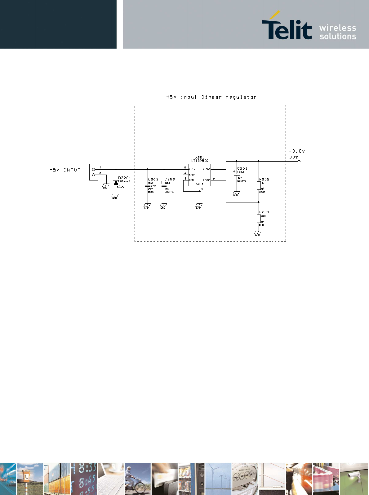
5.4.1.1 + 5V input Source Power Supply Design Guidelines
• The desired output for the power supply is 3.8V, hence there's not a big difference between the
input source and the desired output and a linear regulator can be used. A switching power supply
will not be suited because of the low drop out requirements.
• When using a linear regulator, a proper heat sink shall be provided in order to dissipate the power
generated.
• A Bypass low ESR capacitor of adequate capacity must be provided in order to cut the current
absorption peaks close to the GE863-PRO3 , a 100µF tantalum capacitor is usually suited.
• Make sure the low ESR capacitor on the power supply output (usually a tantalum one) is rated at
least 10V.
• A protection diode should be inserted close to the power input, in order to save the GE863-PRO3
from power polarity inversion.
GE863-PRO
3
Hardware User Guide
1vv0300773a Rev. 1 DRAFT -
24/04/08
Reproduction forbidden without Telit Communications S.p.A. written authorization - All Rights Reserved page 28 of 82
An example of linear regulator with 5V input is:
5.4.1.2 + 12V input Source Power Supply Design Guidelines
• The desired output for the power supply is 3.8V, hence due to the big difference between the input
source and the desired output, a linear regulator is not suited and shall not be used. A switching
power supply will be preferable because of its better efficiency especially with the 2A peak current
load represented by the GE863-PRO3.
• When using a switching regulator, a 500kHz or more switching frequency regulator is preferable
because of its smaller inductor size and its faster transient response. This allows the regulator to
respond quickly to the current peaks absorption.
• For car PB battery the input voltage can rise up to 15,8V and this should be kept in mind when
choosing components: all components in the power supply must withstand this voltage.
• A Bypass low ESR capacitor of adequate capacity must be provided in order to cut the current
absorption peaks, a 100µF tantalum capacitor is usually suited.
• Make sure the low ESR capacitor on the power supply output (usually a tantalum one) is rated at
least 10V.
• For Car applications a spike protection diode should be inserted close to the power input, in order
to clean the supply from spikes.
• A protection diode should be inserted close to the power input, in order to save the GE863-PRO3
from power polarity inversion. This can be the same diode as for spike protection.

GE863-PRO
3
Hardware User Guide
1vv0300773a Rev. 1 DRAFT -
24/04/08
Reproduction forbidden without Telit Communications S.p.A. written authorization - All Rights Reserved page 29 of 82
An example of switching regulator with 12V input is in the below schematic (it is split in 2 parts):

GE863-PRO
3
Hardware User Guide
1vv0300773a Rev. 1 DRAFT -
24/04/08
Reproduction forbidden without Telit Communications S.p.A. written authorization - All Rights Reserved page 30 of 82

GE863-PRO
3
Hardware User Guide
1vv0300773a Rev. 1 DRAFT -
24/04/08
Reproduction forbidden without Telit Communications S.p.A. written authorization - All Rights Reserved page 31 of 82
5.4.1.3 Battery Source Power Supply Design Guidelines
• The desired nominal output for the power supply is 3.8V and the maximum voltage allowed is
4.2V, hence a single 3.7V Li-Ion cell battery type is suited for supplying the power to the Telit
GE863-PRO3 module.
The three cells Ni/Cd or Ni/MH 3,6 V Nom. battery types or 4V PB types MUST NOT BE USED
DIRECTLY since their maximum voltage can rise over the absolute maximum voltage for the
GE863-PRO3 and damage it.
NOTE: DON'T USE any Ni-Cd, Ni-MH, and Pb battery types directly connected with GE863-PRO3 . Their
use can lead to overvoltage on the GE863-PRO3 and damage it. USE ONLY Li-Ion battery types.
• A Bypass low ESR capacitor of adequate capacity must be provided in order to cut the current
absorption peaks, a 100µF tantalum capacitor is usually suited.
• Make sure the low ESR capacitor (usually a tantalum one) is rated at least 10V.
• A protection diode should be inserted close to the power input, in order to save the GE863-PRO3
from power polarity inversion. Otherwise the battery connector should be done in a way to avoid
polarity inversions when connecting the battery.
• The battery capacity must be at least 500mAh in order to withstand the current peaks of 2A; the
suggested capacity is from 500mAh to 1000mAh.
5.4.1.4 Battery Charge control Circuitry Design Guidelines
The charging process for Li-Ion Batteries can be divided into 4 phases:
• Qualification and trickle charging
• Fast charge 1 - constant current
• Final charge - constant voltage or pulsed charging
• Maintenance charge
The qualification process consists in a battery voltage measure, indicating roughly its charge status. If
the battery is deeply discharged, that means its voltage is lower than the trickle charging threshold,
then the charge must start slowly possibly with a current limited pre-charging process where the
current is kept very low with respect to the fast charge value: the trickle charging.
During the trickle charging the voltage across the battery terminals rises; when it reaches the fast
charge threshold level the charging process goes into fast charge phase.
During the fast charge phase the process proceeds with a current limited charging; this current limit
depends on the required time for the complete charge and from the battery pack capacity. During this
phase the voltage across the battery terminals still raises but at a lower rate.
Once the battery voltage reaches its maximum voltage then the process goes into its third state: Final
charging. The voltage measure to change the process status into final charge is very important. It
must be ensured that the maximum battery voltage is never exceeded, otherwise the battery may be
damaged and even explode. Moreover for the constant voltage final chargers, the constant voltage
phase (final charge) must not start before the battery voltage has reached its maximum value,
otherwise the battery capacity will be highly reduced.

GE863-PRO
3
Hardware User Guide
1vv0300773a Rev. 1 DRAFT -
24/04/08
Reproduction forbidden without Telit Communications S.p.A. written authorization - All Rights Reserved page 32 of 82
The final charge can be of two different types: constant voltage or pulsed. GE863-PRO3 uses
constant voltage.
The constant voltage charge proceeds with a fixed voltage regulator (very accurately set to the
maximum battery voltage) and hence the current will decrease while the battery is becoming charged.
When the charging current falls below a certain fraction of the fast charge current value, then the
battery is considered fully charged, the final charge stops and eventually starts the maintenance.
The pulsed charge process has no voltage regulation, instead the charge continues with pulses.
Usually the pulse charge works in the following manner: the charge is stopped for some time, let's say
few hundreds of ms, then the battery voltage will be measured and when it drops below its maximum
value a fixed time length charging pulse is issued. As the battery approaches its full charge the off
time will become longer, hence the duty-cycle of the pulses will decrease. The battery is considered
fully charged when the pulse duty-cycle is less than a threshold value, typically 10%, the pulse charge
stops and eventually the maintenance starts.
The last phase is not properly a charging phase, since the battery at this point is fully charged and the
process may stop after the final charge. The maintenance charge provides an additional charging
process to compensate for the charge leak typical of a Li-Ion battery. It is done by issuing pulses with
a fixed time length, again few hundreds of ms, and a duty-cycle around 5% or less.
This last phase is not implemented in the GE863-PRO3 internal charging algorithm, so that the battery
once charged is left discharging down to a certain threshold so that it is cycled from full charge to
slight discharge even if the battery charger is always inserted. This guarantees that anyway the
remaining charge in the battery is a good percentage and that the battery is not damaged by keeping it
always fully charged (Li-Ion rechargeable battery usually deteriorate when kept fully charged).
Last but not least, in some applications it is highly desired that the charging process restarts when the
battery is discharged and its voltage drops below a certain threshold, GE863-PRO3 internal charger
does it.
As you can see, the charging process is not a trivial task to be done; moreover all these operations
should start only if battery temperature is inside a charging range, usually 5°C - 45°C.
The GE863-PRO3 measures the temperature of its internal component, in order to satisfy this last
requirement, it's not exactly the same as the battery temperature but in common application the two
temperature should not differ too much and the charging temperature range should be guaranteed.
NOTE: For all the threshold voltages, inside the GE863-PRO3 all thresholds are fixed in order to maximize
Li-Ion battery performances and do not need to be changed.
NOTE: In this application the battery charger input current must be limited to less than 400mA. This can
be done by using a current limited wall adapter as the power source.
NOTE: When starting the charger from Module powered off the startup will be in CFUN4; to activate the
normal mode a command AT+CFUN=1 has to be provided. This is also possible using the POWER ON.
There is also the possibility to activate the normal mode using the
ON_OFF* signal.
In this case, when HW powering off the module with the same line (ON_OFF*) and having the charger still
connected, the module will go back to CFUN4.

GE863-PRO
3
Hardware User Guide
1vv0300773a Rev. 1 DRAFT -
24/04/08
Reproduction forbidden without Telit Communications S.p.A. written authorization - All Rights Reserved page 33 of 82
5.4.2 Thermal Design Guidelines
The thermal design for the power supply heat sink should be done with the following specifications:
• Average current consumption during transmission @PWR level max: 500mA
• Average current consumption during transmission @ PWR level min: 100mA
• Average current during Power Saving: 4mA
• Average current during idle (Power Saving disabled) 24mA
• Average current consumption of ARM@ full speed 140 mA
NOTE: The average consumption during transmissions depends on the power level at which the device is
requested to transmit by the network. The average current consumption hence varies significantly.
Considering the very low current during idle, especially if Power Saving function is enabled, it is
possible to consider from the thermal point of view that the device absorbs current significantly only
during calls.
If we assume that the device stays into transmission for short periods of time (let's say few minutes)
and then remains for a quite long time in idle (let's say one hour), then the power supply has always
the time to cool down between the calls and the heat sink could be smaller than the calculated one for
500mA maximum RMS current, or even could be the simple chip package (no heat sink).
Moreover in the average network conditions the device is requested to transmit at a lower power level
than the maximum and hence the current consumption will be less than the 500mA, being usually
around 150mA.
For these reasons the thermal design is rarely a concern and the simple ground plane where the
power supply chip is placed can be enough to ensure a good thermal condition and avoid overheating.
For the heat generated by the GE863-PRO3 , you can consider it to be during transmission 1W max
during CSD/VOICE calls and 2W max during class10 GPRS upload.
This generated heat will be mostly conducted to the ground plane under the GE863-PRO3 ; you must
ensure that your application can dissipate it.

GE863-PRO
3
Hardware User Guide
1vv0300773a Rev. 1 DRAFT -
24/04/08
Reproduction forbidden without Telit Communications S.p.A. written authorization - All Rights Reserved page 34 of 82
5.4.3 Power Supply PCB layout Guidelines
As seen on the electrical design guidelines the power supply shall have a low ESR capacitor on the
output to cut the current peaks and a protection diode on the input to protect the supply from spikes
and polarity inversion. The placement of these components is crucial for the correct working of the
circuitry. A misplaced component can be useless or can even decrease the power supply
performances.
• The Bypass low ESR capacitor must be placed close to the Telit GE863-PRO3 power input pads
or in the case the power supply is a switching type it can be placed close to the inductor to cut the
ripple, provided the PCB trace from the capacitor to the GE863-PRO3 is wide enough to ensure a
dropless connection even during the 2A current peaks.
• The protection diode must be placed close to the input connector where the power source is
drained.
• The PCB traces from the input connector to the power regulator IC must be wide enough to ensure
a minimum voltage drop occur when the 2A current peaks are absorbed. Note that this is not made
in order to save power loss but especially to avoid the voltage drops on the power line at the
current peaks frequency of 216 Hz that will reflect on all the components connected to that supply,
introducing the noise floor at the burst base frequency. For this reason while a voltage drop of 300-
400 mV may be acceptable from the power loss point of view, the same voltage drop may not be
acceptable from the noise point of view. If your application doesn't have audio interface but only
uses the data feature of the Telit GE863-PRO3, then this noise is not so disturbing and power
supply layout design can be more forgiving.
• The PCB traces to the GE863-PRO3 and the Bypass capacitor must be wide enough to ensure no
significant voltage drops occur when the 2A current peaks are absorbed. This is for the same
reason as previous point. Try to keep this trace as short as possible.
• The PCB traces connecting the Switching output to the inductor and the switching diode must be
kept as short as possible by placing the inductor and the diode very close to the power switching
IC (only for switching power supply). This is done in order to reduce the radiated field (noise) at the
switching frequency (100-500 kHz usually).
• The use of a good common ground plane is suggested.
• The placement of the power supply on the board should be done in such a way to guarantee that
the high current return paths in the ground plane are not overlapped to any noise sensitive circuitry
as the microphone amplifier/buffer or earphone amplifier.
• The power supply input cables should be kept separate from noise sensitive lines such as
microphone/earphone cables.
GE863-PRO
3
Hardware User Guide
1vv0300773a Rev. 1 DRAFT -
24/04/08
Reproduction forbidden without Telit Communications S.p.A. written authorization - All Rights Reserved page 35 of 82
6 Antenna
The antenna connection and board layout design are the most important part in the full product design
and they strongly reflect on the product overall performances, hence read carefully and follow the
requirements and the guidelines for a proper design.
6.1 GSM Antenna Requirements
As suggested on the Product Description the antenna and antenna line on PCB for a Telit GE863-
PRO3 device shall fulfil the following requirements:
ANTENNA REQUIREMENTS
Frequency range Depending by frequency band(s) provided by
the network operator, the customer shall use
the most suitable antenna for that/those
band(s)
Bandwidth 70 MHz in GSM850, 80 MHz in GSM900,
170 MHz in DCS & 140 MHz PCS band
Gain Gain < 3dBi
Impedance 50 Ω
Input power > 2 W peak power
VSWR absolute
max <= 10:1
VSWR
recommended <= 2:1
When using the Telit GE863-PRO3, since there's no antenna connector on the module, the antenna
must be connected to the GE863-PRO3 through the PCB with the antenna pad using a 50 Ω
transmission line.
In the case that the antenna is not directly developed on the same PCB, hence directly connected at
the antenna pad of the GE863-PRO3, then a PCB line is needed in order to connect with it or with its
connector.

GE863-PRO
3
Hardware User Guide
1vv0300773a Rev. 1 DRAFT -
24/04/08
Reproduction forbidden without Telit Communications S.p.A. written authorization - All Rights Reserved page 36 of 82
This line of transmission shall fulfil the following requirements:
ANTENNA LINE ON PCB REQUIREMENTS
Impedance 50 ohm
Max Attenuation 0,3 dB
No coupling with other signals allowed
Cold End (Ground Plane) of antenna shall be equipotential to
the GE863-PRO3 ground pins
Furthermore if the device is developed for the US market and/or Canada market, it shall comply to the
FCC and/or IC approval requirements:
This device is to be used only for mobile and fixed application. The antenna(s) used for this transmitter
must be installed to provide a separation distance of at least 20 cm from all persons and must not be
co-located or operating in conjunction with any other antenna or transmitter. OEM integrators must
ensure that the end user has no manual instructions to remove or install the GE863-PRO3 module.
Antennas used for this OEM module must not exceed 3dBi gain for mobile and fixed operating
configurations.
6.2 GSM Antenna - PCB line Guidelines
• Ensure that the antenna line impedance is 50 ohm;
• Keep the antenna line on the PCB as short as possible, since the antenna line loss shall be less
than 0,3 dB;
• Antenna line must have uniform characteristics, constant cross section, avoid meanders and
abrupt curves;
• Keep, if possible, one layer of the PCB used only for the Ground plane;
• Surround (on the sides, over and under) the antenna line on PCB with Ground, avoid having other
signal tracks facing directly the antenna line track;
• The ground around the antenna line on PCB has to be strictly connected to the Ground Plane by
placing vias once per 2mm at least;
• Place EM noisy devices as far as possible from GE863-PRO3 antenna line;
• Keep the antenna line far away from the GE863-PRO3 power supply lines;
• If you have EM noisy devices around the PCB hosting the GE863-PRO3 , such as fast switching
ICs, take care of the shielding of the antenna line by burying it inside the layers of PCB and
surround it with Ground planes, or shield it with a metal frame cover.
• If you don't have EM noisy devices around the PCB of GE863-PRO3 , by using a strip-line on the
superficial copper layer for the antenna line, the line attenuation will be lower than a buried one;

GE863-PRO
3
Hardware User Guide
1vv0300773a Rev. 1 DRAFT -
24/04/08
Reproduction forbidden without Telit Communications S.p.A. written authorization - All Rights Reserved page 37 of 82
6.3 GSM Antenna - installation Guidelines
• Install the antenna in a place covered by the GSM signal.
• The Antenna must be installed to provide a separation distance of at least 20 cm from all persons
and must not be co-located or operating in conjunction with any other antenna or transmitter;
• Antenna shall not be installed inside metal cases
• Antenna shall be installed also according Antenna manufacturer instructions.
6.4 Electro Magnetic Interference - Guidelines
The GE863-PRO
3
has been particularly designed in order to keep to a minimum the Electro Magnetic
Interferences between the ARM part and the GSM/GPRS engine, however especially the ARM part
remains a noisy device that must be threaten with care in order to avoid that its EMI affect the GPRS
part through an external coupling.
Therefore:
• Keep fast ARM lines far away from Antenna line in order to avoid direct coupling;
• Keep fast ARM lines buried in the inner layers, with Ground Layers [fenced with vias] on the
top/bottom layers;
• If your lines are long, place a series resistor [ in the range of 47Ω – 100 Ω ] close to the GE863-
PRO
3
ARM ball to reduce the ringing and the EM emissions of the signal
• If your PCB lines are very long, place a terminator resistor close to the device line end.
GE863-PRO
3
Hardware User Guide
1vv0300773a Rev. 1 DRAFT -
24/04/08
Reproduction forbidden without Telit Communications S.p.A. written authorization - All Rights Reserved page 38 of 82
6.5 Logic level specifications
Where not specifically stated, all the interface circuits work at 2.8V CMOS logic levels. The following
table shows the logic level specifications used in the Telit GE863-PRO3 interface circuits:
Absolute Maximum Ratings -Not Functional
Parameter Min Max
Input level on any
digital pin when on -0.3V +3.6V
Input voltage on
analog pins when on
-0.3V +3.0 V
Voltage on
Buffered
pins -0.3V 25V
Operating Range - Interface levels (CMOS 2.8V)
Level Min Max
Input high level 2.1V 3.3V
Input low level 0V 0.5V
Output high level 2.2V 3.0V
Output low level 0V 0.35V
Operating Range - Interface levels (CMOS 1.8V)
Level Min Max
Input high level 1.6V 3.3V
Input low level 0V 0.4V
Output high level 1,65V 2.2V
Output low level 0V 0.35V
Operating Range - Interface levels (CMOS 3.1V)
Level Min Max
Input high level 2.0V 3.4V
Input low level -0.3V 0.8V
Output high level 2.7V 3.2V
Output low level 0V 0.4V
GE863-PRO
3
Hardware User Guide
1vv0300773a Rev. 1 DRAFT -
24/04/08
Reproduction forbidden without Telit Communications S.p.A. written authorization - All Rights Reserved page 39 of 82
Operating Range - Interface levels (CMOS 1.8V-A)
Level Min Max
Input high level 1.3V 2.1V
Input low level -0.3V 0.5V
Output high level 1.35V 1.9V
Output low level 0V 0.45V
Operating Range - Interface levels (CMOS VRTC)
Level Min Max
Input high level 1.3V 2.1V
Input low level -0.3V 0.5V
Output high level 1.3V 2.0V
Output low level 0V 0.5V
GSM GPIO Current characteristics
Level Typical
Output Current 1mA
Input Current 1uA
CMOS 3.1V Current characteristics
Level Typical
Max Output Current 16 mA
Input Current 1uA
CMOS 1.8V-A Current characteristics
Level Typical
Max Output Current 4 mA
Input Current 1uA
GE863-PRO
3
Hardware User Guide
1vv0300773a Rev. 1 DRAFT -
24/04/08
Reproduction forbidden without Telit Communications S.p.A. written authorization - All Rights Reserved page 40 of 82
6.5.1 GSM Reset signal
Signal Function I/O Bga Ball
RESET*-GSM
Phone reset I E5
RESET*-GSM is used to reset the GE863-PRO
3
modules GSM engine. Whenever this signal is pulled low,
the GSM/GPRS engine is reset. When the device is reset it stops any operation. After the release of
the reset the GSM/GPRS engine is unconditionally shut down, without doing any detach operation
from the network where it is registered. This behaviour is not a proper shut down because any GSM
device is requested to issue a detach request on turn off. For this reason the Reset signal must not be
used to normally shutting down the device, but only as an emergency exit in the rare case the device
remains stuck waiting for some network response.
The RESET*-GSM is internally controlled on start-up to achieve always a proper power-on reset
sequence, so there's no need to control this pin on start-up. It may only be used to reset a device
already on that is not responding to any command.
NOTE: do not use this signal to power off the GE863-PRO3 GSM engine. Use the ON/OFF*-GSM signal to
perform this function or the AT#SHDN command.
Reset Signal Operating levels:
Signal Min Max
RESET Input high 2.0V* 2.2V
RESET Input low 0V 0.2V
* this signal is internally pulled up so the pin can be left floating if not used.
If unused, this signal may be left unconnected. If used, then it must always be connected with an
open collector transistor, to permit to the internal circuitry the power on reset and under voltage
lockout functions.

GE863-PRO
3
Hardware User Guide
1vv0300773a Rev. 1 DRAFT -
24/04/08
Reproduction forbidden without Telit Communications S.p.A. written authorization - All Rights Reserved page 41 of 82
7 Serial Ports
The serial port on the Telit GE863-PRO3 is the core of the interface between the module engine and
the ARM processor.
2 serial ports are available on the module engine:
• MODEM SERIAL PORT
• MODEM SERIAL PORT 2 (DEBUG)
6+1(DBG) serial ports are available on the ARM part.
No direct connection is present between the two parts, on the hosting PCB the two serial ports need to
be interconnected. It is up to the user to select whatever serial port is most suited on the ARM part to
exchange data with the GPRS engine; however the USART0 port on the ARM is the only supporting
the full RS232 line signaling and should be preferred.
In the ball-out of the GE863-PRO3 the balls of the MODEM SERIAL port and ARM USART0 are
placed one next the other, allowing an easy routing of the connection.
7.1 MODEM SERIAL PORT
Several configurations can be designed for the serial port on the OEM hardware, but the most
common are:
• RS232 PC com port
• microcontroller UART @ 2.8V – 3.1V (Universal Asynchronous Receive Transmit)
Depending from the type of serial port on the OEM hardware a level translator circuit may be needed
to make the system work. The only configuration that doesn't need a level translation is the 2.8V –
3.1V UART and hence the GE863-PRO3 GPRS engine can be directly connected with the ARM serial
port @ 3.1V CMOS.
The serial port on the GE863-PRO3 GPRS engine is a +2.8V UART with all the 7 RS232 signals,
While the serial ports on the ARM part are +3.1V UART.
GE863-PRO3 serial ports differ from the PC-RS232 in the signal polarity (RS232 is reversed) and
levels. The levels for the GE863-PRO3 UART are the CMOS levels:
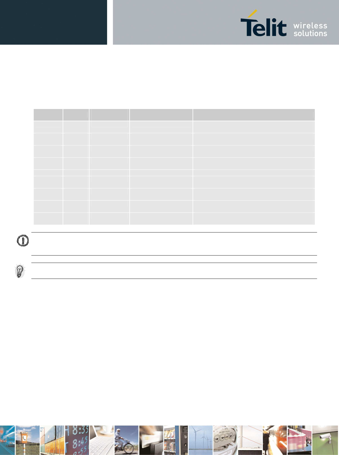
GE863-PRO
3
Hardware User Guide
1vv0300773a Rev. 1 DRAFT -
24/04/08
Reproduction forbidden without Telit Communications S.p.A. written authorization - All Rights Reserved page 42 of 82
The signals of the GE863-PRO3 GPRS engine serial port are:
RS232 Pin
Number Signal GE863-PRO3
Ball Name Usage
1 DCD -
dcd_uart C7 Data Carrier Detect Output from the GE863-PRO3 GPRS engine that
indicates the carrier presence
2 RXD -
tx_uart E10 Transmit line *see Note Output transmit line of GE863-PRO3 GPRS engine
3 TXD -
rx_uart E9 Receive line *see Note Input receive of the GE863-PRO3 GPRS engine
4 DTR -
dtr_uart C6 Data Terminal Ready Input to the GE863-PRO3 GPRS engine that
controls the DTE READY condition
5 GND All GND Ground Ground
6 DSR -
dsr_uart C5 Data Set Ready Output from the GE863-PRO3 GPRS engine that
indicates the module is ready
7 RTS -
rts_uart C8 Request to Send Input to the GE863-PRO3 GPRS engine that
controls the Hardware flow control
8 CTS -
cts_uart C9 Clear to Send Output from the GE863-PRO3 GPRS engine that
controls the Hardware flow control
9 RI -
ri_uart C4 Ring Indicator Output from the GE863-PRO3 GPRS engine that
indicates the incoming call condition
NOTE: According to V.24, RX/TX signal names are referred to the application side, therefore on the GE863-PRO3
GPRS engine side these signal are on the opposite direction: TXD on the ARM application side will be connected to
the receive line (here named TXD/ rx_uart ) of the GE863-PRO3 GPRS engine serial port and viceversa for RX.
TIP: For a minimum implementation, only the TXD and RXD lines can be connected, the other lines can be left open
provided a software flow control is implemented.

GE863-PRO
3
Hardware User Guide
1vv0300773a Rev. 1 DRAFT -
24/04/08
Reproduction forbidden without Telit Communications S.p.A. written authorization - All Rights Reserved page 43 of 82
7.2 RS232 level translation
In order to interface the Telit GE863-PRO3 with a PC com port or a RS232 (EIA/TIA-232) application a
level translator is required. This level translator must
• invert the electrical signal in both directions
• change the level from 0/3V to +15/-15V
Actually, the RS232 UART 16450, 16550, 16650 & 16750 chipsets accept signals with lower levels on
the RS232 side (EIA/TIA-562) , allowing for a lower voltage-multiplying ratio on the level translator.
Note that the negative signal voltage must be less than 0V and hence some sort of level translation is
always required.
The simplest way to translate the levels and invert the signal is by using a single chip level translator.
There are a multitude of them, differing in the number of driver and receiver and in the levels (be sure
to get a true RS232 level translator not a RS485 or other standards).
By convention the driver is the level translator from the 0-3V UART level to the RS232 level, while the
receiver is the translator from RS232 level to 0-3V UART.
In order to translate the whole set of control lines of the UART you will need:
• 5 driver
• 3 receiver
NOTE: The digital input lines working at 2.8V/3.1VCMOS have an absolute maximum input voltage of
3,75V; therefore the level translator IC shall not be powered by the +3.8V supply of the module. Instead it
shall be powered from a +2.8V / +3.1V (dedicated or 3.1V_OUT) power supply.
This is because in this way the level translator IC outputs on the module side (i.e. GE863-PRO3 inputs) will
work at +3.8V interface levels, stressing the module inputs at its maximum input voltage.
This can be acceptable for evaluation purposes, but not on production devices.
NOTE: In order to be able to do in circuit reprogramming of the GE863-PRO3 GPRS firmware, the serial
port on the Telit GE863-PRO3 shall be available for translation into RS232 and either it's controlling ARM
device shall be placed into tristate, disconnected or as a gateway for the serial data when module
reprogramming occurs.
Only RXD, TXD, GND and the On/off module turn on pad are required to the reprogramming of the module,
the other lines are unused.
All applicator shall include in their design such a way of reprogramming the GE863-PRO3 .
NOTE: In order to be able to do in circuit reprogramming of the GE863-PRO3 ARM Application software,
the serial port DEBUG on the Telit GE863-PRO3 shall be available for translation into RS232 when module
reprogramming occurs.
Only DRXD, DTXD, GND and the On/off*-AP module turn on pad are required to the reprogramming of the
module, the other lines are unused.
All applicator shall include in their design such a way of reprogramming the GE863-PRO3.
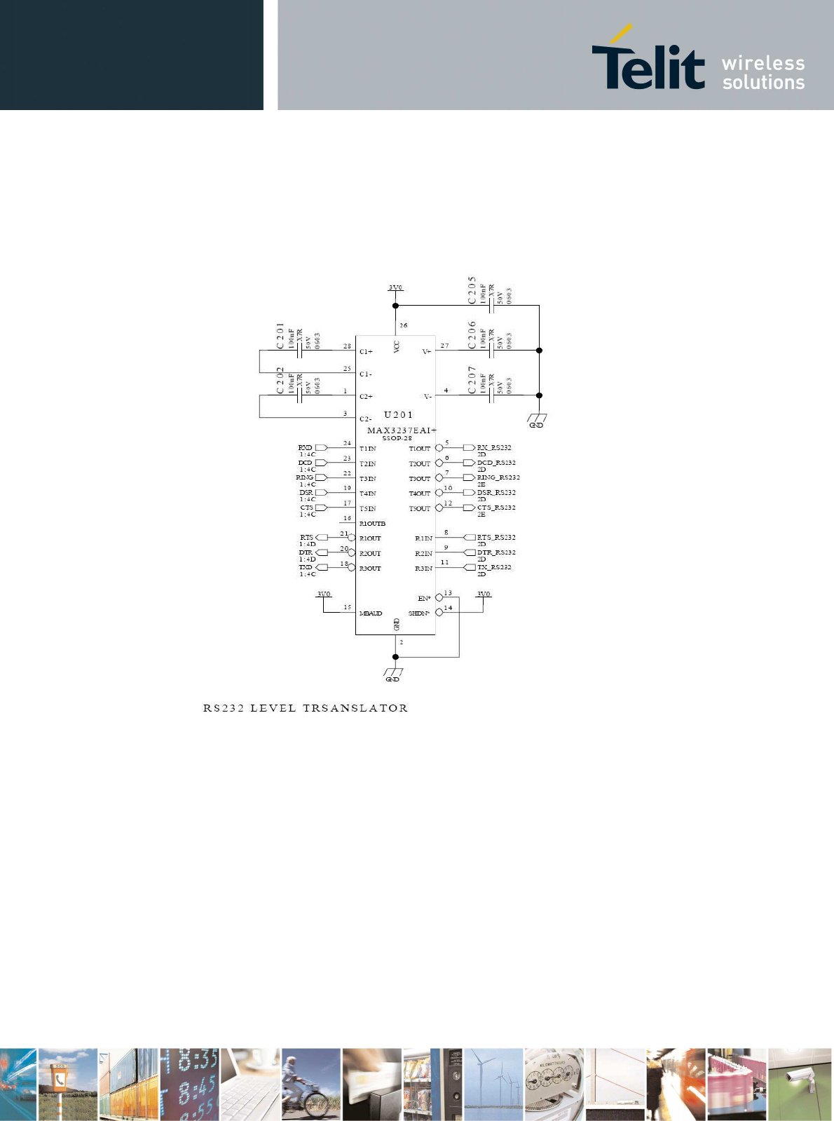
GE863-PRO
3
Hardware User Guide
1vv0300773a Rev. 1 DRAFT -
24/04/08
Reproduction forbidden without Telit Communications S.p.A. written authorization - All Rights Reserved page 44 of 82
An example of level translation circuitry of this kind is:

GE863-PRO
3
Hardware User Guide
1vv0300773a Rev. 1 DRAFT -
24/04/08
Reproduction forbidden without Telit Communications S.p.A. written authorization - All Rights Reserved page 45 of 82
The RS232 serial port lines are usually connected to a DB9 connector with the following layout:

GE863-PRO
3
Hardware User Guide
1vv0300773a Rev. 1 DRAFT -
24/04/08
Reproduction forbidden without Telit Communications S.p.A. written authorization - All Rights Reserved page 46 of 82
8 Audio Section Overview
The Base Band Chip of the GE863-PRO3 GPRS engine provides two different audio blocks; both in
transmit (Uplink) and in receive (Downlink) direction:
“MT lines” should be used for handset function,
“HF lines” is suited for hands -free function (car kit).
These two blocks can be active only one at a time, selectable by AT command. The audio
characteristics are equivalent in transmit blocks, but are different in the receive ones and this should
be kept in mind when designing.

GE863-PRO
3
Hardware User Guide
1vv0300773a Rev. 1 DRAFT -
24/04/08
Reproduction forbidden without Telit Communications S.p.A. written authorization - All Rights Reserved page 47 of 82
8.1 Microphone Paths Characteristic and Requirements
TIP: being the microphone circuitry the more noise sensitive, its design and layout must be
done with particular care. Both microphone paths are balanced and the OEM circuitry should
be balanced designed to reduce the common mode noise typically generated on the ground
plane. However also an unbalanced circuitry can be used for particular OEM application needs
.
TIP: due to the difference in the echo canceller type, the “Mic_MT” audio path is suited for
Handset applications, while the “Mic_HF”audio path is suited for hands-free function (car kit).
The Earphone applications should be made using the “Mic_HF” audio path but DISABLING the
echo canceller by software AT command. If the echo canceller is left active with the Earphone,
then some echo might be introduced by the echo cancel algorithm.
“Mic_MT” 1
st
differential microphone path
• line coupling AC
• line type balanced
• coupling capacitor ≥ 100nF
• differential input resistance 50kΩ
• differential input voltage ≤ 1,03V
pp
(365mV
rms
)
• microphone nominal sensitivity -45 dBV
rms
/Pa
• analog g
ain suggested
+ 20dB
• echo canceller type handset
“Mic_HF” 2
nd
differential microphone path
• line coupling AC
• line type balanced
• coupling capacitor ≥ 100nF
• differential input resistance 50kΩ
• differential input voltage ≤ 65mV
pp
(23mV
rms
)
• microphone nominal sensitivity -45 dBV
rms
/Pa
• analog
gain suggested
+10dB
• echo canceller type car kit hands-free
GE863-PRO
3
Hardware User Guide
1vv0300773a Rev. 1 DRAFT -
24/04/08
Reproduction forbidden without Telit Communications S.p.A. written authorization - All Rights Reserved page 48 of 82
TIP: definition of the nominal sensitivity of the microphone lines .
The nominal sensitivity of the microphone lines indicates the voltage level on the GE863-PRO3 pins
present during "normal spoken" conditions.
For a handset , the "normal spoken” conditions take place when the talker mouth is 7cm far from the
microphone ; under these conditions the voice will produce an acoustic pressure of -4,7dBPa @1kHz
on the microphone membrane .
TIP: electrical equivalent signal and operating voice levels .
At "normal spoken" conditions, a microphone having the suggested nominal sensitivity of -
45dBV
rms
/Pa , will produce
the electrical equivalent signal :
that means :
During a call, this level varies according to the volume of the talker voice; usually the following rough
thumb rule for the dynamic range may be used :
1) the talker is screaming . This is the strongest voice level condition: the signal increases by
+20dB;
2) the talker is whispering. This is the lowest voice level condition: the voice level decreases by –
50dB.
These changes must be considered for designing the external microphone amplifier.
TIP: example of external microphone amplifier calculation .
Let’s suppose to use the 1
st
differential microphone path .In this case the maximum differential input
voltage to “Mic_MT” lines is 365mV
rms
(1,03V
pp
) corresponding to –8,76dBV.
Now we can calculate the maximum voltage gain of an external microphone amplifier G
A
:
(
)
[
]
dBVGdBMicLevel
A
76,820 −=++
[
]
76,8207,49 −=++−
A
G
A
G−=+− 209,40
dBG
A
94,20=
you can set G
A
= +20dB to use standard resistor values .
MicLevel = ( -45) + (-4.7) = -49.7 dB
Vrms
MicVoltage = 10
(
-
49.7 / 20 )
= 3.3* 10
-
3
V
rms
GE863-PRO
3
Hardware User Guide
1vv0300773a Rev. 1 DRAFT -
24/04/08
Reproduction forbidden without Telit Communications S.p.A. written authorization - All Rights Reserved page 49 of 82
TIP: environment consideration .
For hands-free/car kit microphone, you must take into account the voice attenuation, due to the
distance between the microphone itself and the talker, when designing the external microphone
amplifier.
Not only, you must consider that the microphone will pick up also ambient noise; to overcome this
problem it is preferable to set the gain of the microphone 10dB lower with respect to the calculated
value for a nominal sensitivity. The corresponding reduction in signal level will be compensated by an
increased voice volume of the talker which will speak louder because of the ambient noise.
For a car cabin usually the distance between the microphone itself and the talker is 40/50cm ; in these
conditions the attenuation can be considered as a thumb rule around 20dB .
For the earphone we shall distinguish two different types: the earphones having the microphone
sustained close to the mouth and the ones having the microphone on the earpiece cable.
The same considerations for the additional voice attenuation due to the distance from the microphone
and the noise pick up can be made for the earphone having the microphone on the earpiece cable,
while the other kind of earphone shall be threaten as a handset.
TIP: how to compensate the losses in car cabin hands-free condition.
The voice signal , that in the "normal spoken” conditions produces on the microphone membrane an
acoustic pressure of -4,7dBPa at 1kHz , will have a further attenuation of 20dB due the 50cm distance
.
Therefore a microphone having the suggested nominal sensitivity of -45dBV
rms
/Pa,will produce a lower
electrical
equivalent signal :
that means :
Setting the “microphone gain” at +10dB (3 times), the signal in the nominal conditions on the
“Mic_HF” inputs s of GE863-PRO3 Telit Module will be :
Hence in these conditions the signal level on the“Mic_HF” input pads of the GE863-PRO3 is 10 dB (3
times) lower than the nominal, as suggested.
MicLevel = ( -45) + (-4.7)-20 = -69.7
dBV
MicVoltage = 10
(
-
49.7 / 20 )
= 0,33* 10
-
3
V
“Mic_HF” Level = 0,33* 10
-
3
* 3=1* 10
-
3
V

GE863-PRO
3
Hardware User Guide
1vv0300773a Rev. 1 DRAFT -
24/04/08
Reproduction forbidden without Telit Communications S.p.A. written authorization - All Rights Reserved page 50 of 82
8.2 General Design Rules
There are several configurations for the audio paths, but the most effective difference is between
balanced and unbalanced microphone configuration.
It is highly recommended to keep the whole microphone path balanced even if this means having 2
wires connecting the microphone instead of one needed (plus ground) in the unbalanced case. The
balanced circuitry is more suited because of its good common mode noise rejection, reducing the 216
Hz burst noise produced during the GSM transmissions.
• Where possible use balanced microphone circuitry
• Keep the microphone traces on the PCB and wires as short as possible.
• If your application requires an unbalanced microphone, then keep the lines on the PCB balanced
and "unbalance" the path close to the microphone wire connector if possible.
• For the microphone biasing voltage use a dedicated voltage regulator and a capacitor multiply
circuit.
• Make sure that the microphone traces in the PCB don't cross or run parallel to noisy traces
(especially the power line)
• If possible put all around to the microphone lines a ground trace connected to the ground plane by
several vias. This is done in order to simulate a shielded trace on the PCB.
• The biasing circuit and eventually the buffer can be designed in the same manner for the internal
and external microphones.
8.3 Other considerations
If your application is a hands-free/car kit scenario , but you need to put microphone and speaker
inside the same box :
• try to have the maximum possible distance between them, at least 7cm ;
• since the microphone type is very important, if you use an omni-directional one ( and this is the
typical application ) please seal it on the rear side (no back cavity) in order not to collect unwanted
signals ;
• try to make divergent the main axes of the two devices .

GE863-PRO
3
Hardware User Guide
1vv0300773a Rev. 1 DRAFT -
24/04/08
Reproduction forbidden without Telit Communications S.p.A. written authorization - All Rights Reserved page 51 of 82
8.4 Microphone Biasing
The electret microphones usually need a biasing voltage to work properly. Refer to your microphone
provider for the characteristics required.
NOTE: The microphones have a hot wire were the positive biasing must be connected. Usually
it is indicated by a + symbol or a red point. If the polarity of the bias is reversed, then the
microphone will not work properly. For this reason be sure to respect the mic. biasing polarity.
8.4.1 Balanced Microphone Biasing
The balanced microphone bias voltage should be obtained from a dedicated voltage regulator, in order
to eliminate the noise present on the power lines. This regulator can be the same for all the audio
paths. The microphone should be supplied from a capacitor multiply circuit.
For example a circuit for the balanced microphone biasing can be:
NOTE: In the balanced application the resistors R2 and R3 must have the same value to keep
the circuit balanced.
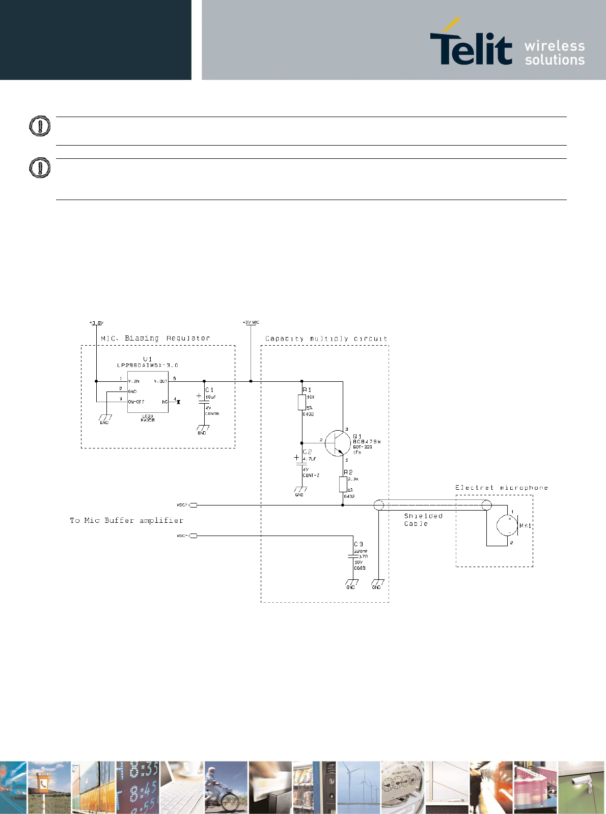
GE863-PRO
3
Hardware User Guide
1vv0300773a Rev. 1 DRAFT -
24/04/08
Reproduction forbidden without Telit Communications S.p.A. written authorization - All Rights Reserved page 52 of 82
NOTE: The cable to the microphone should not be shielded, instead a twisted pair cable shall
be used.
NOTE: The microphone sensitivity changes with the value of R2 and R3. Usually the
microphones are characterized with 2kΩ biasing resistance, so try to keep the sum of R2 and
R3 around 2kΩ. Refer to your microphone manufacturer for the mic. characteristics.
8.4.2 Unbalanced Microphone Biasing
The unbalanced microphone biasing voltage should be obtained from a dedicated voltage regulator, in
order to eliminate the noise present on the power lines. This regulator can be the same for all the
audio paths. The microphone should be supplied from a capacitor multiply circuit.
For example a circuit for the unbalanced microphone biasing can be:

GE863-PRO
3
Hardware User Guide
1vv0300773a Rev. 1 DRAFT -
24/04/08
Reproduction forbidden without Telit Communications S.p.A. written authorization - All Rights Reserved page 53 of 82
NOTE: In the unbalanced application the capacitor C3 shall be > 200nF otherwise the frequency
response will be cut at low band frequencies (down to 300Hz). This capacitor can be placed
close to the MIC- pad (MIC_HF- or MIC_MT- depending on the audio path chosen) or if
possible it should be placed close to the shielded cable connector. If the ground return path is
well designed, then it is possible to eliminate the C3 capacitor, provided the buffer is close to
the mic. input.
NOTE: The cable to the microphone should be shielded.
NOTE: The microphone changes with the value of R2. Usually the microphone sensitivity is
characterized with 2kΩ biasing resistance, so try to keep the value of R2 around 2kΩ. For mic.
characteristics refer to the manufacturer.
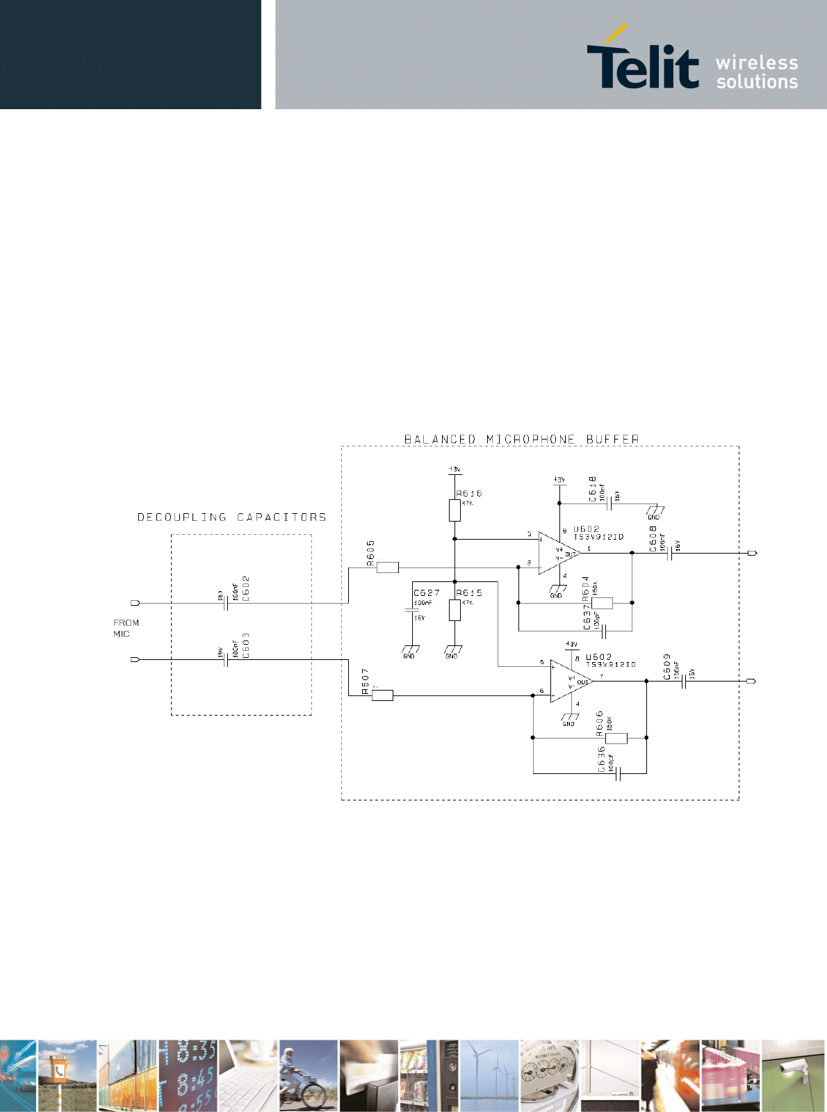
GE863-PRO
3
Hardware User Guide
1vv0300773a Rev. 1 DRAFT -
24/04/08
Reproduction forbidden without Telit Communications S.p.A. written authorization - All Rights Reserved page 54 of 82
8.5 Microphone Buffering
As seen previously, a microphone shall be connected to the input pins of the GE863-PRO3 through a
buffer amplifier that boosts the signal level to the required value.
Again the buffered microphone circuitry can be balanced or unbalanced: where possible it is always
preferable a balanced solution. The buffering circuit shall be placed close to the microphone or close
to the microphone wire connector.
8.5.1 Buffered Balanced Mic
A sample circuit can be:
This circuit has a gain of 10 times (+20 dB), and is therefore suited for the “Mic_MT “ input if you have
a microphone with a sensitivity close to the suggested one (-45 dBV
rms/
Pa). If your microphone has a
different sensitivity or if the buffer is connected to the “Mic_HF “ inputs , then a gain adjustment shall
be done by changing resistors R604 and R606 ( if the required value is not a standard one , you can
change R605 e R607 ) and as a consequence the capacitors C636 and C637 to maintain the
bandwidth 150-4000Hz (at -3dB).
270pF
270pF
+20dB
15K
15K
to
GE863

GE863-PRO
3
Hardware User Guide
1vv0300773a Rev. 1 DRAFT -
24/04/08
Reproduction forbidden without Telit Communications S.p.A. written authorization - All Rights Reserved page 55 of 82
The buffer gain is given by the formula:
607
606
605
604
R
R
R
R
Gain ==
The C636 and C637 capacitors are placed in order to cut off the gain at higher frequencies than the
transmitted GSM band, the cutoff frequency (-3dB) should be 3500Hz in order to have -1dB at 3kHz.
The cutoff frequency is given by the formula:
636
*
606
*
2
1
637
*
604
*
2
1
.
C
R
C
R
freq
ππ
==
[Hz]
TIP: example of calculation .
Let's assume you have a microphone with a sensitivity of -45 dBV
rms
/Pa and you want to use it in 1st
differential microphone path (“Mic_MT” inputs) in "normal spoken" conditions at acoustic pressure of
-4.7dBPa.
As reported at page 33 , the electrical level output from the microphone will be :
corresponding to:
When the talker is screaming ,we will have a signal of 330 mV
rms
on the “Mic_MT “ inputs due to a
20dB higher Mic Level (see TIP 1) with a buffer gain G
A
:
G
A
=20 log (AmplifierOutput / MicVoltage) =20 log (330 * 10
-3
)/( 33 * 10
-3
) = 20 log 10=20dB
The corresponding values for the resistors on the buffer could be ( if we keep the input resistance
10kΩ )
R604 = R606 = gain* R607= gain* R605 = 10* 15 = 150 kΩ
The commercial values of 150kΩ & 15kΩ are then chosen.
As a consequence the values of the capacitors C636 and C637 shall be:
C636=C637= 1/ (2π*4000*R606)= 265 *10
-12
F
A commercial value of 270pF gives a cutoff frequency of 3931Hz with an errorless than 1,8% .
MicLevel = ( -45) + (-4.7) = -49.7 dB
Vrms
MicVoltage = 10
(
-
49.7 / 20 )
= 3.3* 10
-
3
V
rms
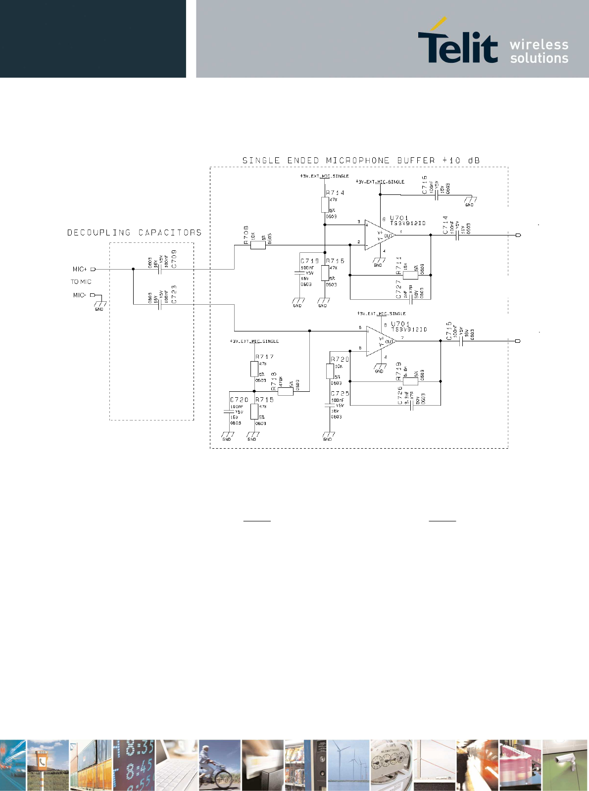
GE863-PRO
3
Hardware User Guide
1vv0300773a Rev. 1 DRAFT -
24/04/08
Reproduction forbidden without Telit Communications S.p.A. written authorization - All Rights Reserved page 56 of 82
8.5.2 Buffered Unbalanced (Single Ended) Microphone
The above schematic can be used for a single ended (buffered unbalanced) microphone; the required
biasing circuitry is not included. Note also that the capacitor C3 is not needed.
The gains of the two amplifiers are given by the formulas:
( )
720
719
1buffer invertingnot
R
R
Gain +=
( )
708
711
buffer inverting
R
R
Gain =
Assigning half of overall gain to each amplifier, you will obtain the requested gain because of doubling
the microphone signal path; in fact by the use of two amplifiers (the upper as “inverting” and the lower
as “not inverting” configuration ) we obtain an additional +6dB gain (2 times) .
Remember: the “not inverting“ amplifier section gain shall not be less than 1 .
Like for the balanced buffered microphone, the amplifier overall gain can be modify changing the value
of resistor R719/R720 and R711 and as a consequence the capacitors C726 and C727. It is
advisable to change R708 only if you have difficulty to find a commercial value for R711; in this case
change R708 as little as possible.
The -3dB bandwidth is given by the approximated formula (considering C725 >> C726):
2,7nF
6,8nF
To
GE863
GE863
Mic+
GE863
Mic-

GE863-PRO
3
Hardware User Guide
1vv0300773a Rev. 1 DRAFT -
24/04/08
Reproduction forbidden without Telit Communications S.p.A. written authorization - All Rights Reserved page 57 of 82
727
*
711
*
2
1
726
*
719
*
2
1
.
C
R
C
R
freq
ππ
==
[Hz]
The buffer bandwidth at -3dB shall be 4KHz.
Note that the biasing of the operational amplifier is given for the inverting amplifier by the series divider
R714-R715. The 100nF capacitor C719 is needed to filter the noise that could be coupled to that
divider. For the not inverting operational amplifier the biasing is given by a different divider R715-R717
with the capacitor C720 and through a series resistor R718 of 470KΩ.
TIP: example of calculation.
Llet's assume you have a microphone with a sensitivity of -45dBV
rms
/Pa and you want to use it in 2nd
differential microphone path (“Mic_HF” inputs) in "normal spoken" conditions at acoustic pressure
of -4.7dBPa.
As reported at page XX , the electrical level output from the microphone will be :
but we have to consider 20dB loss due to the higher distance from the mouth of the talker ( 50cm ) .
corresponding to
In order to have a signal of 1 mV
rms
at the “Mic_HF” inputs , as suggested at TIP “environment
consideration “,
the buffer must have a gain or +10 dB
Keeping in mind that “ balancing the line will double the signal”, to calculate the resistor values assign
half of required gain G
A
to each amplifier section . And therefore G
S
=1,5times (or +3,52dB) .
Choosing as 10kΩ as the input resistance , the corresponding values for the resistors on the buffer will
be :
R711 = G
S
* R708= 1.5*10 =15 kΩ
R719 = (G
S
-1) * R720 = (1.5 -1)*10 =5 kΩ
The commercial values of 15kΩ and 5.6kΩ be accepted .
As a consequence of the assigned values of the resistors, the nominal values of C726 and C727 are
:
MicLevel = ( -45) + (-4.7) = -49.7 dBV
rms
MicVoltage = 10
(
-
69.7 / 20 )
= 0,33* 10
-
3
V
MicLevel = ( -49.7) + (-20) = -69.7 dBV
rms
G
A
= “Mic_HF /MicVoltage = (1*10
-
3
)/(0,33*10
-
3
)=3

GE863-PRO
3
Hardware User Guide
1vv0300773a Rev. 1 DRAFT -
24/04/08
Reproduction forbidden without Telit Communications S.p.A. written authorization - All Rights Reserved page 58 of 82
C726= 1/ (2π*4000*R719)= 7.10 *10
-9
F
C727= 1/ (2π*4000*R711)= 2,65 *10
-9
F
modified in 6,8nF (f
c1
=4181Hz ) and 2,7nF (f
c2
=3931Hz) because of commercial values .

GE863-PRO
3
Hardware User Guide
1vv0300773a Rev. 1 DRAFT -
24/04/08
Reproduction forbidden without Telit Communications S.p.A. written authorization - All Rights Reserved page 59 of 82
9 OUTPUT LINES (Speaker)
9.1 Short description
The Telit GE863-PRO3 provides two audio paths in receive section. Only one of the two paths can be
active at a time, selectable by AXE hardware line or by AT command.
You must keep in mind the different audio characteristics of the receive blocks when designing:
the “Ear_MT” lines EPN1 and EPP1 are the Differential Line-Out Drivers ; they can drive an
external amplifier or directly a 16 Ω earpiece at –12dBFS (*) ;
the “Ear_HF” lines EPPA1_2 and EPPA2 are the Fully Differential Power Buffers ; they can directly
drive a 16Ω speaker in differential (balanced) or single ended (unbalanced) operation mode .
(*) FS : acronym of Full Scale. It is equal to 0dB, the maximum Hardware Analog Receive Gain of
BaseBand Chip.
The “Ear_MT” audio path should be used for handset function, while the “Ear_HF” audio path is suited
for hands-free function (car kit).
Both receiver outputs are B.T.L. type (Bridged Tie Load) and the OEM circuitry shall be designed
bridged to reduce the common mode noise typically generated on the ground plane and to get the
maximum power output from the device; however also a single ended circuitry can be designed for
particular OEM application needs.

GE863-PRO
3
Hardware User Guide
1vv0300773a Rev. 1 DRAFT -
24/04/08
Reproduction forbidden without Telit Communications S.p.A. written authorization - All Rights Reserved page 60 of 82
9.2 Output Lines Characteristics
“Ear_MT” Differential Line-out Drivers Path
• line coupling: DC
• line type: bridged
• output load resistance : ≥ 14 Ω
• internal output resistance: 4 Ω (typical)
• signal bandwidth: 150 - 4000 Hz @ -3 dB
• max. differential output voltage 1310 mV
rms
(typ, open circuit)
• differential output voltage 328mVrms /16 Ω @ -12dBFS
• SW volume level step - 2 dB
• number of SW volume steps 10
“Ear_HF” Power Buffers path
• line coupling: DC
• line type: bridged
• output load resistance : ≥ 14 Ω
• internal output resistance: 4 Ω ( >1,7 Ω )
• signal bandwidth: 150 - 4000 Hz @ -3 dB
• max. differential output voltage 1310 mV
rms
(typ, open circuit)
• max. single ended output voltage 656 mV
rms
(typ, open circuit)
• SW volume level step - 2 dB
• number of SW volume steps 10

GE863-PRO
3
Hardware User Guide
1vv0300773a Rev. 1 DRAFT -
24/04/08
Reproduction forbidden without Telit Communications S.p.A. written authorization - All Rights Reserved page 61 of 82
9.3 General Design Rules
There are several configurations for the audio output path, but the various design requirements can be
grouped into three different categories:
• handset earphone (low power, typically a handset)
• hands-free earphone (low power, typically a earphone)
• car kit speakerphone (high power, typically a speaker)
The three groups have different power requirements, usually the first two applications need only few
mW of power, which can be directly drained from the GE863-PRO3 pads, provided a suited speaker is
used. This direct connect design is the cheaper and simpler solution and will be suited for the most of
the earphone design requirements. There's no need to decouple the output ear lines if a suited
earpiece is connected. For the last group, the speakerphone, a power amplifier is required to raise the
output power up to 5-10W required in a car cabin application.
All the designs shall comply with the following guidelines:
• Where possible use a bridged earphone circuitry, to achieve the maximum power output from the
device.
• Keep the earphone traces on the PCB and wires as short as possible.
• If your application requires a single ended earpiece and you want a direct connection, then leave
one of the two output lines open and use only the other referred to ground. Remember that in this
case the power output is 4 times lower than the bridged circuit and may not be enough to ensure
a good voice volume.
• Make sure that the earphone traces in the PCB don't cross or run parallel to noisy traces
(especially the power line)
• The cable to the speaker shall be a twisted pair with both the lines floating for the bridged output
type, shielded with the shield to ground for the single ended output type.
9.3.1 Noise Filtering
The I/O of the PCB should have a noise filter close to the connector, to filter the high frequency GSM
noise. The filter can be a Π formed by 2 capacitor and a inductance, with the one capacitor of 39pF -
0603 case, and the other capacitor of 1nF - 0603; the inductance shall have a value of 39µH .

GE863-PRO
3
Hardware User Guide
1vv0300773a Rev. 1 DRAFT -
24/04/08
Reproduction forbidden without Telit Communications S.p.A. written authorization - All Rights Reserved page 62 of 82
9.4 Handset Earphone Design
As seen previously, a 16Ω earpiece can be directly connected to the output pads EAR_MT+ and
EAR_MT- of the GE863-PRO3.
This solution is often the more cost effective, reducing the components count to a minimum. There are
several limitations to the use of this solution: speaker direct connect imposes the speaker
characteristics to be almost exactly the suggested ones, otherwise the power output may be reduced
(if speaker impedance is bigger than 16Ω) or the GE863-PRO3 ear port may be damaged (if speaker
impedance is less than 15Ω).
The other limitation of the speaker direct connection is the power output capability of the GE863-
PRO3 which is limited and for some particular applications may not be enough.
For these reasons, when the power output of the GE863-PRO3 is not enough or if the speaker
characteristics are different from the suggested, then it is preferable to use an amplifier to increase the
power and current output capabilities.
Again the output from the GE863-PRO3 is bridged and both lines should be used, where possible, as
inputs to the power amplifier. This ensures a higher common mode rejection ratio, reducing the GSM
current busts noise on the speaker output.
In this case the “EAR_MT” lines from the GE863-PRO3 should be AC coupled with a ceramic
capacitor of 100nF (or bigger ) .
It is always desirable to have a mute control on the amplifier, in order to turn it off while the device is
not sending signal to the output, in this manner the amplifier background noise which may be audible
during idle conditions is cut off.
A principle schematic may be:
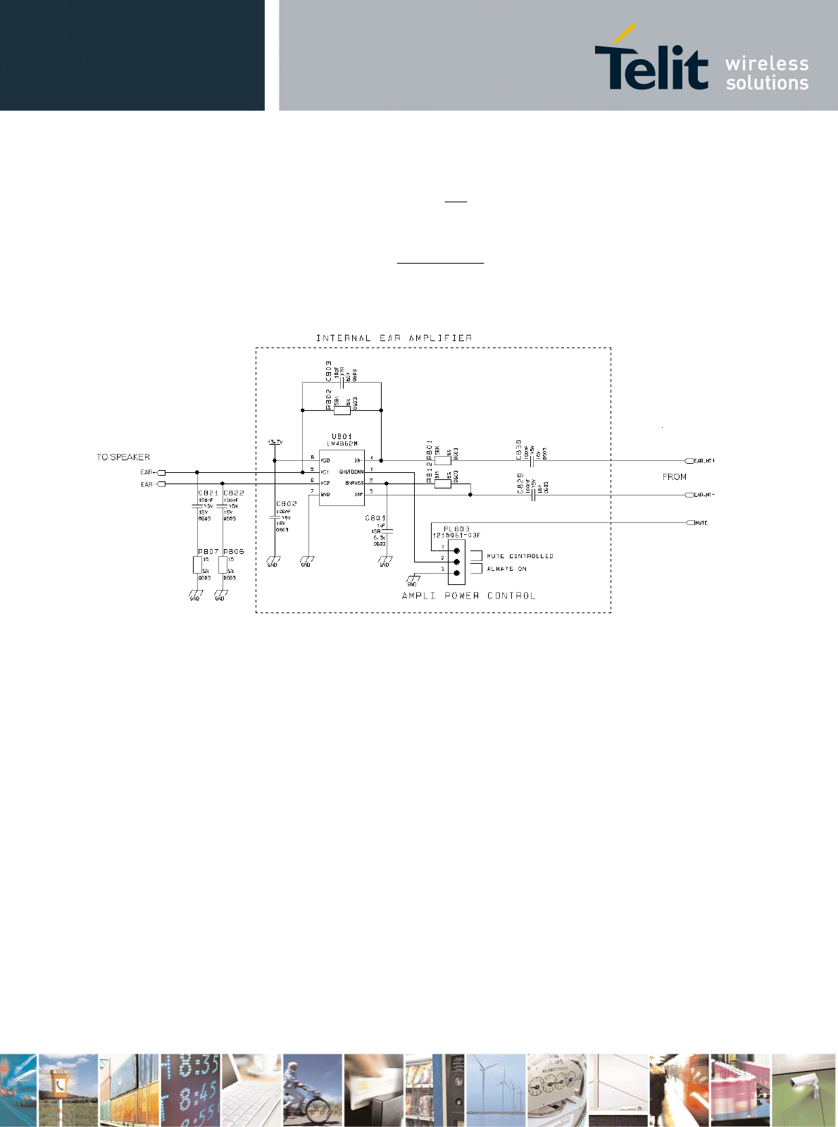
GE863-PRO
3
Hardware User Guide
1vv0300773a Rev. 1 DRAFT -
24/04/08
Reproduction forbidden without Telit Communications S.p.A. written authorization - All Rights Reserved page 63 of 82
The resulting gain and high pass cut can be obtained with the formula:
2
3
R
R
Gain =
4
*
3
*
2
1
.
C
R
freq
π
=
[Hz]
And an example of internal Ear amplifier could be:
Some amplifier require a low impedance load at high frequency in order to avoid auto oscillation, this
can be made with a capacitor (100nF) in series with a resistor (15Ω).
When designing your application, remember to provide an adequate bypass capacitor to the amplifier
and place it close to the power input pin of the IC, keeping the traces as short as possible.
9.5 Hands-Free Earphone (Low Power) Design
The same design considerations made for the handset are valid for the hands-free earphone.
+12dB
GE863-PRO3
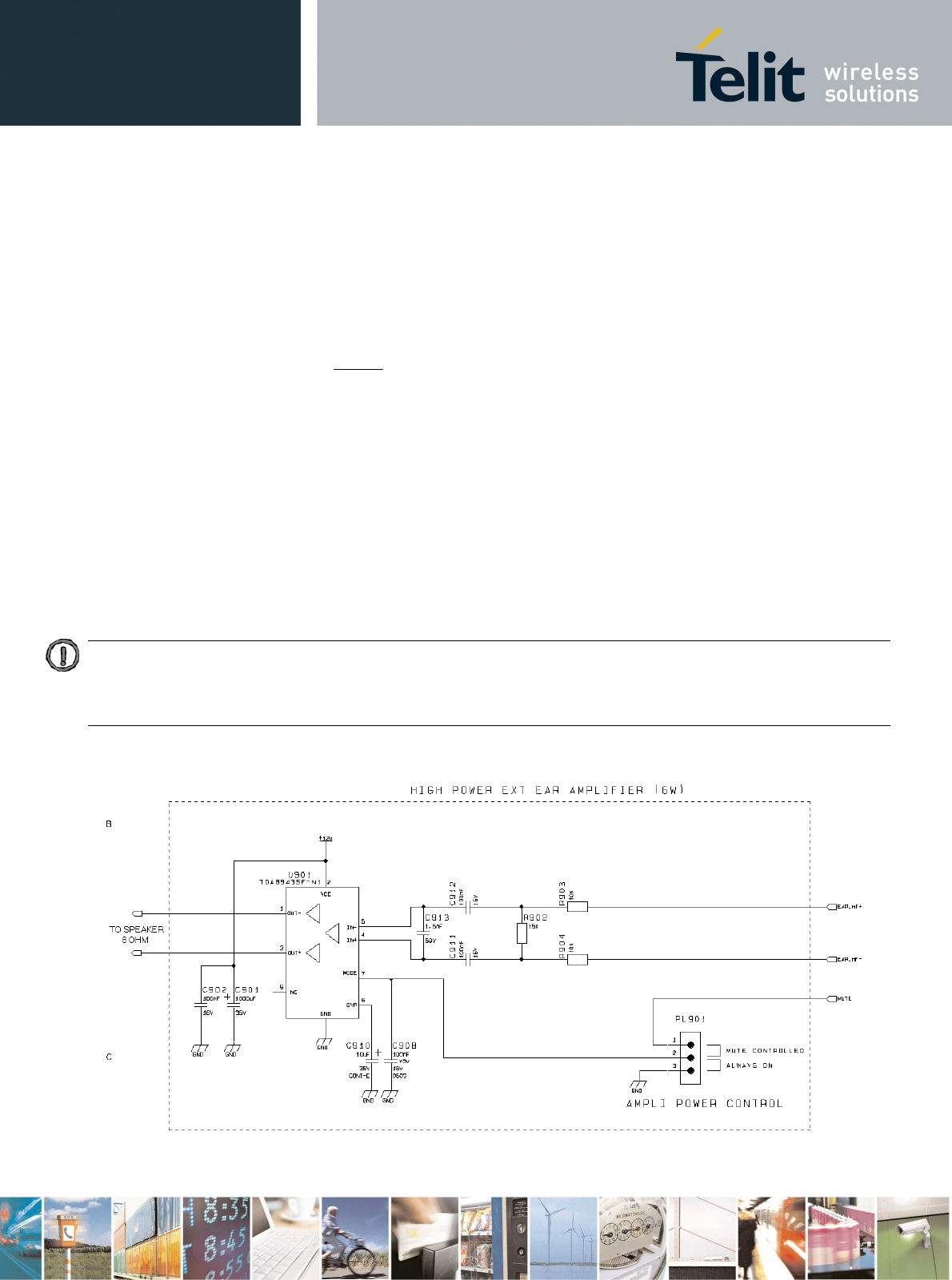
GE863-PRO
3
Hardware User Guide
1vv0300773a Rev. 1 DRAFT -
24/04/08
Reproduction forbidden without Telit Communications S.p.A. written authorization - All Rights Reserved page 64 of 82
9.6 Car Kit Speakerphone Design
For the car kit speaker phone function the power output requirement is usually at least 4W, therefore
an amplifier is needed to boost the GE863-PRO3 output.
The design of the amplifier shall comply with the following guidelines:
• The input to the amplifier MUST be taken from the “Ear_HF” audio path of the GE863-PRO3,
because of its echo canceller parameters suited to a car cabin use.
• The amplifier shall have a gain of 30-40 times (29-32 dB) to provide the desired output power of 5-
10W with the signal from the GE863-PRO3 “Ear_HF” audio output lines.
• If the amplifier has a fixed gain then it can be adjusted to the desired value by reducing the input
signal with a resistor divider network.
• The amplifier shall have a mute control to be used while not in conversation. This results in two
benefits: eliminating the background noise when not in conversation and saving power.
• The power to the amplifier should be decoupled as much as possible from the GE863-PRO3
power supply, by either keeping separate wires and placing bypass capacitors of adequate value
close to the amplifier power input pads.
• The biasing voltage of the amplifier shall be stabilized with a low ESR (e.g. a tantalum) capacitor of
adequate value.
NOTE: The GE863-PRO3 audio path connected to the car kit hands-free amplifier MUST be
“Ear_HF” one, otherwise the echo cancellation will not be done due to the difference in the
echo canceller characteristics of the GE863-PRO3 internal audio path from the external audio
path.
Example of car kit amplifier schematic.

GE863-PRO
3
Hardware User Guide
1vv0300773a Rev. 1 DRAFT -
24/04/08
Reproduction forbidden without Telit Communications S.p.A. written authorization - All Rights Reserved page 65 of 82
9.7 The Evaluation Kit for Telit GE863-PRO
3
Modules
9.7.1 Short Description
Telit supplies the Evaluation Kit for Telit GE863-PRO
3
modules to assist the designer in developing his
own applications based on GE863-PRO
3
Telit module.
The GE863-PRO
3
EVK is formed by a mother board and a dedicated Telit module Interface Board
with RF antenna connectors.
It provides a fully functional solution for a complete M2M application.
The motherboard has a power supply and is equipped with SIM card housing, RS 232 serial port level
translator, direct USB2.0 Host & Device connection, Smartcard ISO7816 slot, SD-MMC Card slot and
10/100 Mb Ethernet.
The only items you have to provide are:
1) a personal computer or microcontroller ;
2) a SIM card with a valid Network subscription;
3) a power supply
The connection between the GE863-PRO
3
EVK and your PC (or other DTE) are realized by standard
RS232 ports.
The communications between the application ARM and Telit GPRS Engine is realized connecting the
Asynchronous Serial Interfaces of the module’s ARM&GSM/GPRS by setting appropriately the
Jumpers.
Furthermore the communications between ARM and GSM/GPRS can be analyzed with two “sniffed”
serial ports that can report both sides of the ARM-GSM/GPRS serial channel.

GE863-PRO
3
Hardware User Guide
1vv0300773a Rev. 1 DRAFT -
24/04/08
Reproduction forbidden without Telit Communications S.p.A. written authorization - All Rights Reserved page 66 of 82
10 General Purpose I/O
The general purpose I/O pads can be configured to act in three different ways:
• input
• output
• alternate function (internally controlled)
The following GPIO are available on the GE863-PRO3 :
Ball Signal I/O Function Type Input /
output
current
Default
State
ON_OFF
state
State
during
Reset Note
E6 GPIO1 I/O GPIO01 Configurable GPIO CMOS 2.8V
1uA / 1mA INPUT LOW Alternate function
(JDR)
55 GPIO2 I/O GPIO02 Configurable GPIO CMOS 2.8V
1uA / 1mA INPUT HIGH HIGH 4.7K Pull Up
32 GPIO3 I/O GPIO03 Configurable GPIO CMOS 2.8V
1uA / 1mA INPUT LOW Alternate function
(RFTXMON)
53 GPIO4 I/O GPIO05 Configurable GPIO CMOS 2.8V
1uA / 1mA INPUT LOW Alternate function
(BUZZER)
54 GPIO5 I/O GPIO06 Configurable GPIO CMOS 2.8V
1uA / 1mA INPUT LOW
51 GPIO6 I/O GPIO07 Configurable GPIO CMOS 2.8V
1uA / 1mA INPUT LOW
6 GPIO7 I/O GPIO08 Configurable GPIO CMOS 2.8V
1uA / 1mA INPUT LOW Alternate function
(RF Transmission
Control)
5 GPIO8 I/O GPIO09 Configurable GPIO CMOS 2.8V
1uA / 1mA INPUT LOW
4 GPIO9 I/O GPIO10 Configurable GPIO CMOS 2.8V
1uA / 1mA INPUT LOW
Input pads can only be read and report the digital value (high or low) present on the pad at the read
time; output pads can only be written or queried and set the value of the pad output; an alternate
function pad is internally controlled by the GE863-PRO3 firmware and acts depending on the function
implemented.

GE863-PRO
3
Hardware User Guide
1vv0300773a Rev. 1 DRAFT -
24/04/08
Reproduction forbidden without Telit Communications S.p.A. written authorization - All Rights Reserved page 67 of 82
All GPIO pads are 2.8V CMOS signals and their interface levels are the same specified in the
paragraph 6.5.
10.1 Using a GPIO Pad as INPUT
The GPIO pads, when used as inputs, can be connected to a digital output of another device and
report its status, provided this device has interface levels compatible with the 2.8V CMOS levels of the
GPIO.
If the digital output of the device to be connected with the GPIO input pad has interface levels different
from the 2.8V CMOS, then it can be buffered with an open collector transistor with a 47K pull up to
2.8V.
10.2 Using a GPIO Pad as OUTPUT
The GPIO pads, when used as outputs, can drive 2.8V CMOS digital devices or compatible hardware.
When set as outputs, the pads have a push-pull output and therefore the pull-up resistor may be
omitted.
10.3 Using the RF Transmission Control GPIO7
The GPIO7 pin, when configured as RF Transmission Control Input, permits to disable the Transmitter
when the GPIO is set to Low by the application.
10.4 Using the RFTXMON Output GPIO3
The GPIO3 pin, when configured as RFTXMON Output, is controlled by the GE863-PRO3 module and
will rise when the transmitter is active and fall after the transmitter activity is completed.
For example, if a call is started, the line will be HIGH during all the conversation and it will be again
LOW after hanged up.
The line rises up 300ms before first TX burst and will became again LOW from 500ms to 1sec after
last TX burst.
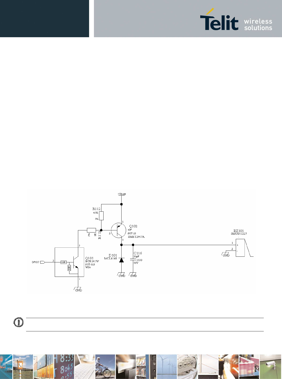
GE863-PRO
3
Hardware User Guide
1vv0300773a Rev. 1 DRAFT -
24/04/08
Reproduction forbidden without Telit Communications S.p.A. written authorization - All Rights Reserved page 68 of 82
10.5 Using the Alarm Output
The GPRS Engine GPIO pads, when configured as Alarm Output, can be controlled by the GE863-
PRO3 module and will rise when the alarm starts and fall after the issue of a dedicated AT command.
This output can be used to power up the GE863-PRO3 application processor at the alarm time, giving
you the possibility to program a timely system wake-up to achieve some periodic actions and
completely turn off both the application processor and the GE863-PRO3 during sleep periods,
dramatically reducing the sleep consumption to few µA.
In battery-powered devices this feature will greatly improve the autonomy of the device.
10.6 Using the Buzzer Output GPIO4
The GPIO4 pad, when configured as Buzzer Output, is controlled by the GE863-PRO3 module and
will drive with appropriate square waves a Buzzer driver.
This permits to your application to easily implement Buzzer feature with ringing tones or melody
played at the call incoming, tone playing on SMS incoming or simply playing a tone or melody when
needed by your application.
A sample interface scheme is included below to give you an idea of how to interface a Buzzer to the
GPIO7:
NOTE: To correctly drive a buzzer a driver must be provided, its characteristics depend on the Buzzer and for them
refer to your buzzer vendor.
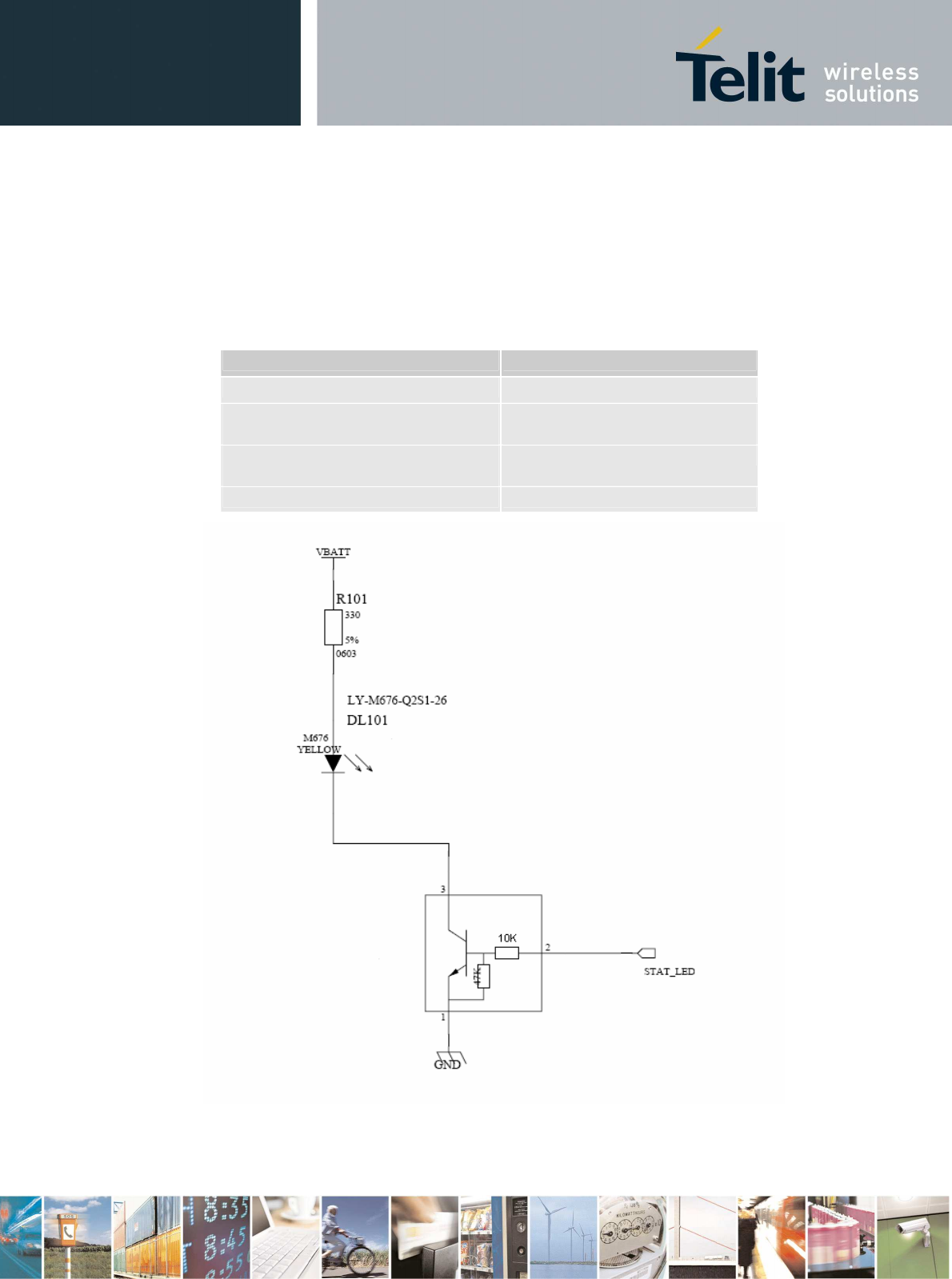
GE863-PRO
3
Hardware User Guide
1vv0300773a Rev. 1 DRAFT -
24/04/08
Reproduction forbidden without Telit Communications S.p.A. written authorization - All Rights Reserved page 69 of 82
10.7 Indication of network service availability
The STAT_LED pin status shows information on the network service availability and Call status.
In the GE863 modules, the STAT_LED usually needs an external transistor to drive an external LED.
Therefore, the status indicated in the following table is reversed with respect to the pin status.
LED status Device Status
Permanently off Device off
Fast blinking
(Period 1s, Ton 0,5s) Net search / Not registered /
turning off
Slow blinking
(Period 3s, Ton 0,3s) Registered full service
Permanently on a call is active
10.8
GE863-PRO
3
Hardware User Guide
1vv0300773a Rev. 1 DRAFT -
24/04/08
Reproduction forbidden without Telit Communications S.p.A. written authorization - All Rights Reserved page 70 of 82
RTC Bypass out
The VRTC pin brings out the Real Time Clock supply, which is separate from the rest of the digital
part, allowing having only RTC going on when all the other parts of the device are off.
To this power output a backup capacitor can be added in order to increase the RTC autonomy during
power off of the battery. NO Devices must be powered from this pin.
10.9 VAUX1 power output
A regulated power supply output is provided in order to supply small devices from the module.
This output is active when the module is ON and goes OFF when the module is shut down.
The operating range characteristics of the supply are:
Operating Range – VAUX1 power supply
Min Typical Max
Output voltage 2.75V 2.85V 2.95V
Output current 100mA
Output bypass capacitor 2.2µF

GE863-PRO
3
Hardware User Guide
1vv0300773a Rev. 1 DRAFT -
24/04/08
Reproduction forbidden without Telit Communications S.p.A. written authorization - All Rights Reserved page 71 of 82
11 Mounting the GE863-PRO
3
on the
Application Board
11.1 General
The Telit GE863-PRO3 module has been designed in order to be compliant with a standard lead-free SMT
process
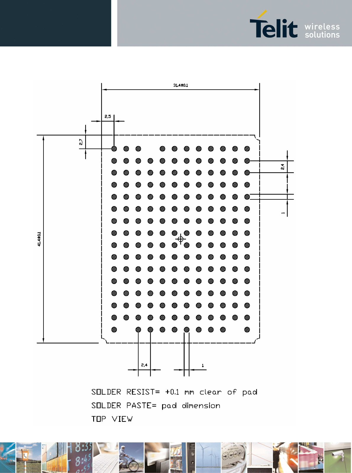
GE863-PRO
3
Hardware User Guide
1vv0300773a Rev. 1 DRAFT -
24/04/08
Reproduction forbidden without Telit Communications S.p.A. written authorization - All Rights Reserved page 72 of 82
11.1.1 Recommended footprint for the application
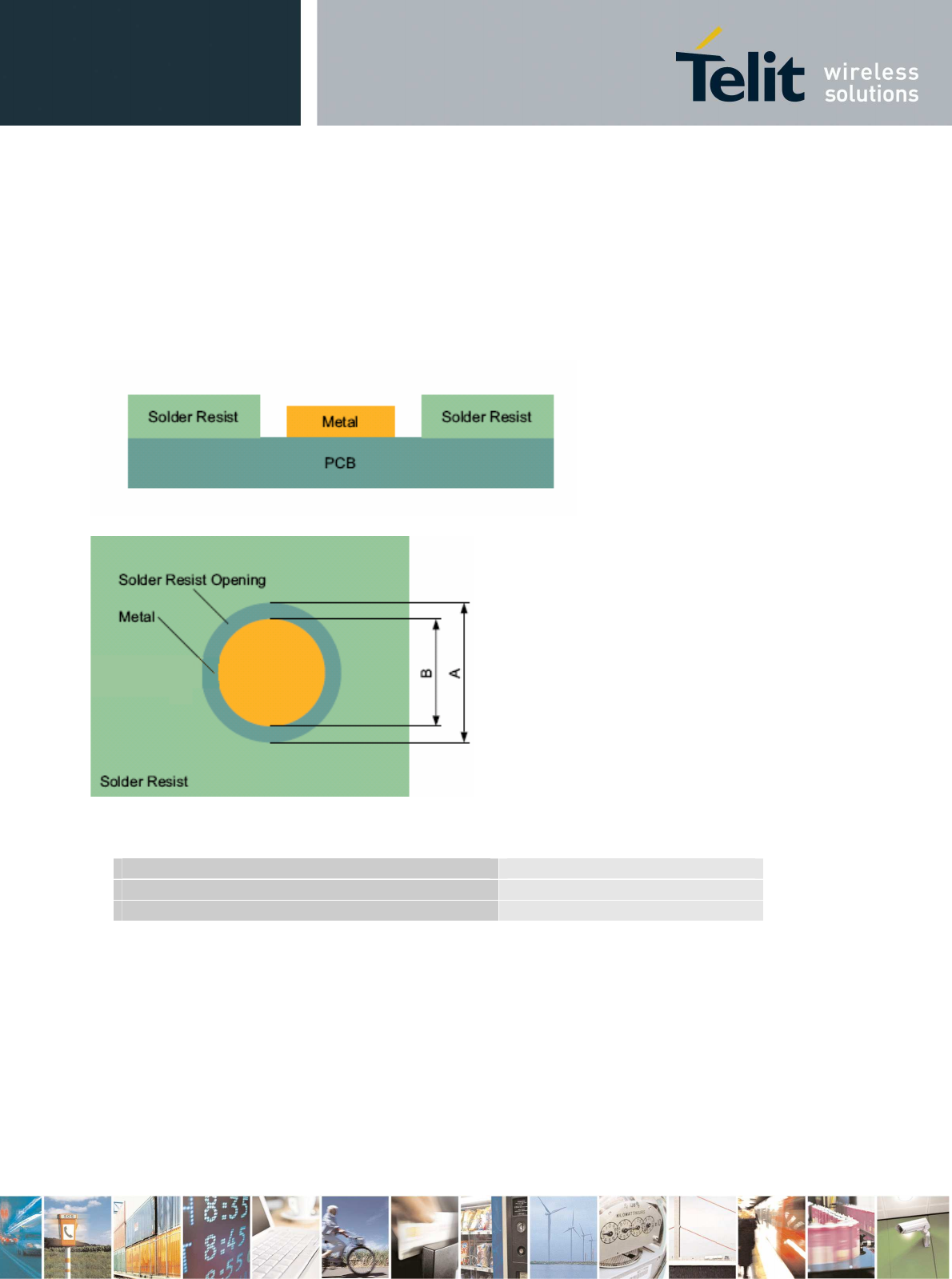
GE863-PRO
3
Hardware User Guide
1vv0300773a Rev. 1 DRAFT -
24/04/08
Reproduction forbidden without Telit Communications S.p.A. written authorization - All Rights Reserved page 73 of 82
11.1.2 Stencil
Stencil’s apertures layout can be the same of the recommended footprint (1:1), we suggest a
thickness of stencil foil ≥ 120µm.
11.1.3 PCB pad Design
“Non solder mask defined” (NSMD) type is recommended for the solder pads on the PCB.
Recommendations for PCB pad dimensions
Ball pitch [mm] 2,4
Solder resist opening diameter A [mm] 1,10
Metal pad diameter B [mm] 1 ± 0.05
Placement of microvias not covered by solder resist is not recommended inside the “Solder resist
opening”, unless the microvia carry the same signal of the pad itself.
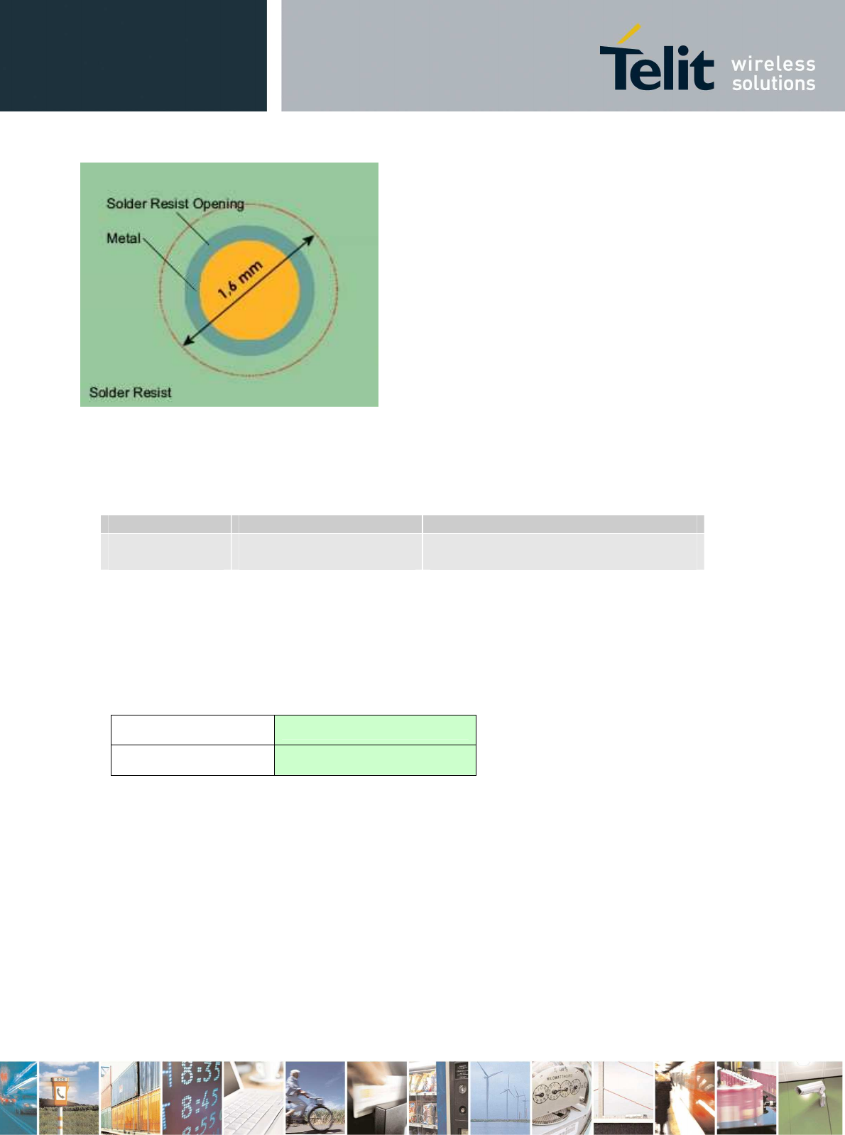
GE863-PRO
3
Hardware User Guide
1vv0300773a Rev. 1 DRAFT -
24/04/08
Reproduction forbidden without Telit Communications S.p.A. written authorization - All Rights Reserved page 74 of 82
Holes in pad are allowed only for blind holes and not for through holes.
Recommendations for PCB pad surfaces:
Finish Layer thickness [µm] Properties
Electro-less Ni /
Immersion Au 3 –7 /
0.05 – 0.15 good solder ability protection, high
shear force values
The PCB must be able to resist the higher temperatures, which are occurring at the lead-free process.
This issue should be discussed with the PCB-supplier. Generally, the wet-ability of tin-lead solder
paste on the described surface plating is better compared to lead-free solder paste.
11.1.4 Solder paste
Lead free
Solder paste Sn/Ag/Cu
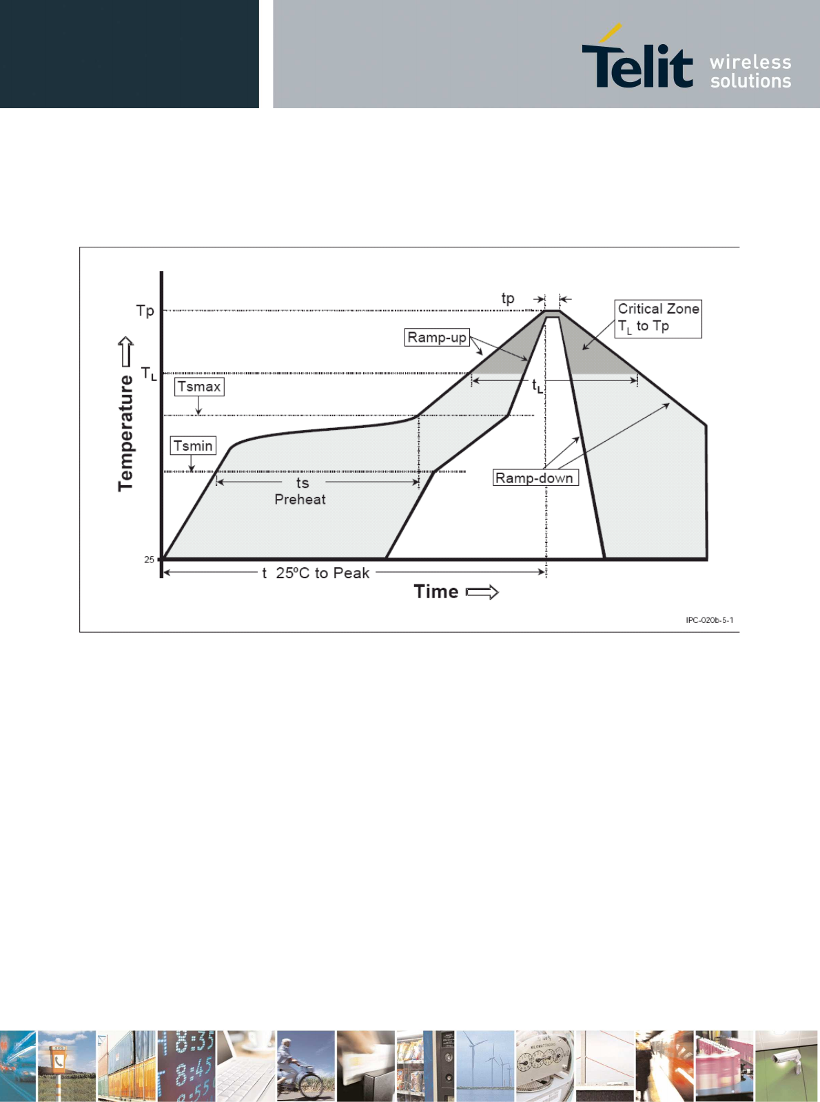
GE863-PRO
3
Hardware User Guide
1vv0300773a Rev. 1 DRAFT -
24/04/08
Reproduction forbidden without Telit Communications S.p.A. written authorization - All Rights Reserved page 75 of 82
11.1.5 GE863-PRO3 Solder Reflow
The following is the recommended solder reflow profile
GE863-PRO
3
Hardware User Guide
1vv0300773a Rev. 1 DRAFT -
24/04/08
Reproduction forbidden without Telit Communications S.p.A. written authorization - All Rights Reserved page 76 of 82
Profile Feature Pb-Free Assembly
Average ramp-up rate (T
L
to T
P
) 3°C/second max
Preheat:
– Temperature Min (Tsmin)
– Temperature Max (Tsmax)
– Time (min to max) (ts)
150°C
200°C
60-180 seconds
Tsmax to TL:
– Ramp-up Rate
3°C/second max
Time maintained above:
– Temperature (TL)
– Time (tL)
217°C
60-150 seconds
Peak Temperature (Tp): 245 +0/-5°C
Time within 5°C of actual Peak
Temperature (tp) 10-30 seconds
Ramp-down Rate 6°C/second max.
Time 25°C to Peak Temperature
8 minutes max.
NOTE: All temperatures refer to topside of the package, measured on the package body surface.
NOTE: GE863-PRO3 module can accept only one reflow process
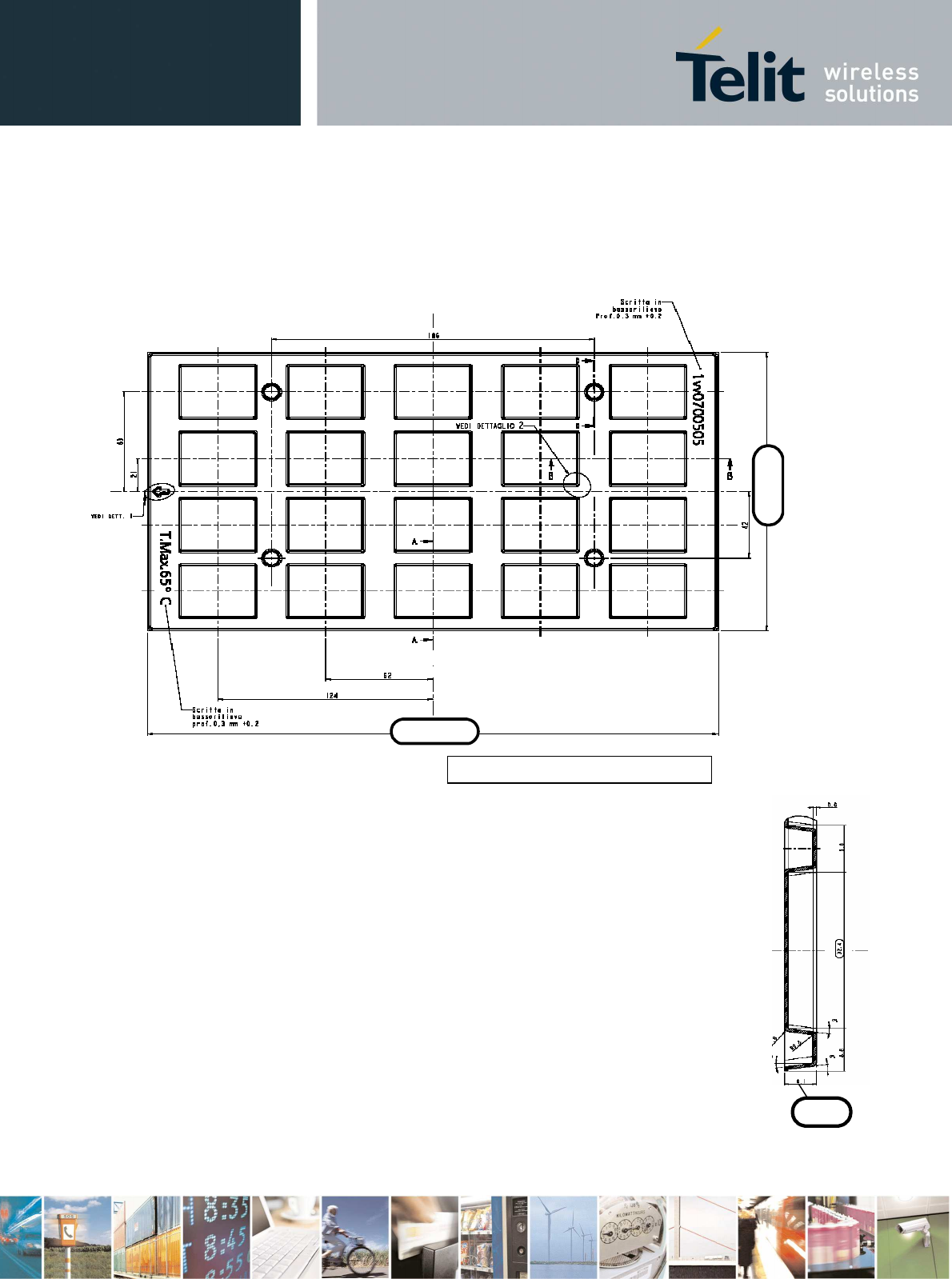
GE863-PRO
3
Hardware User Guide
1vv0300773a Rev. 1 DRAFT -
24/04/08
Reproduction forbidden without Telit Communications S.p.A. written authorization - All Rights Reserved page 77 of 82
11.1.6 Packing System
According to SMT processes for pick & place movement requirements, Telit GE863-PRO3 modules are
packaged on trays, each tray contains 20 pieces. Tray dimensions are:
Note that trays can withstand a maximum temperature of 65° C.
320 ± 0,3
170 ± 0,3
All quotes are in mm, general tolerance ± 0.1
6.1
Section A-A
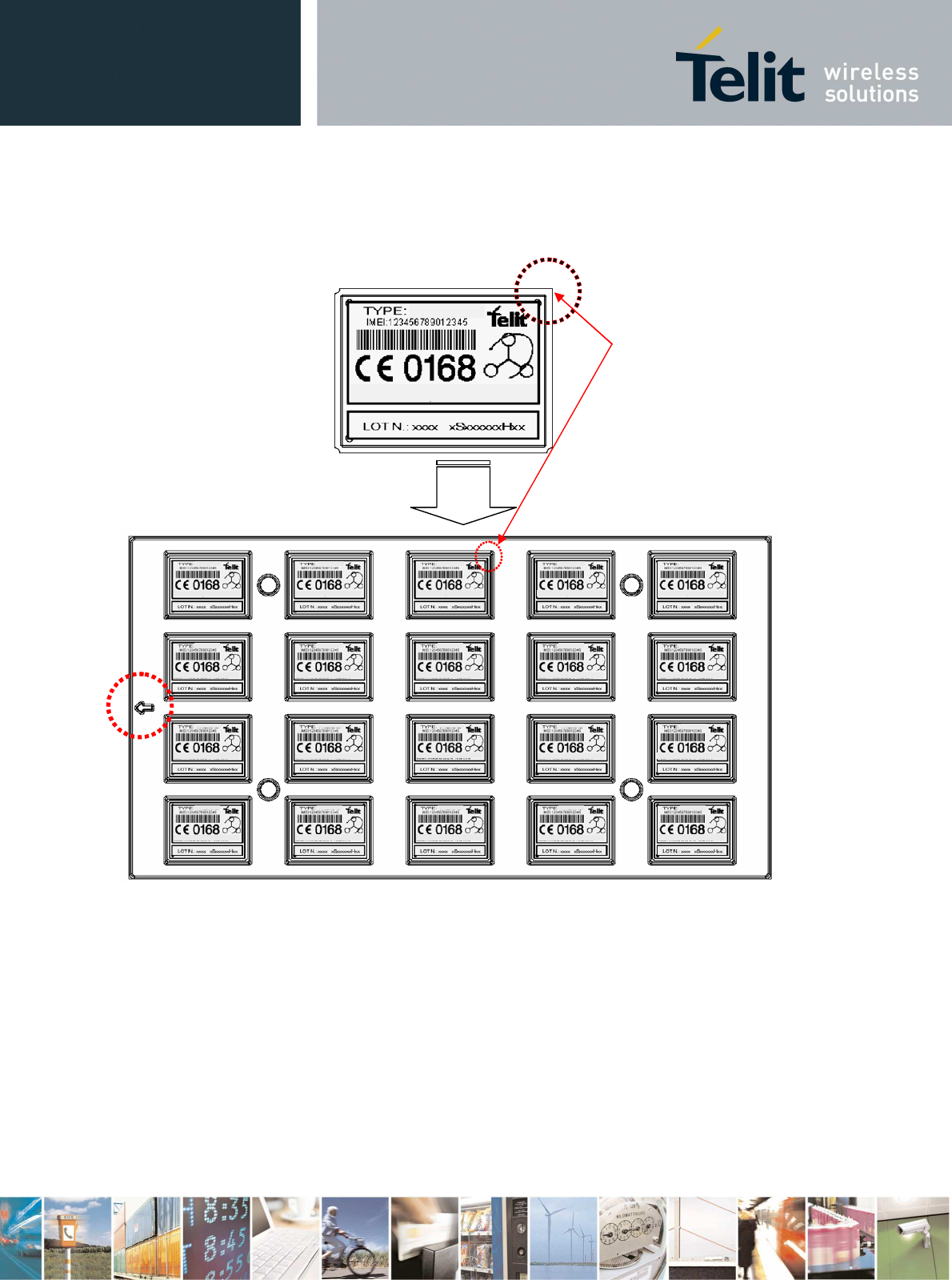
GE863-PRO
3
Hardware User Guide
1vv0300773a Rev. 1 DRAFT -
24/04/08
Reproduction forbidden without Telit Communications S.p.A. written authorization - All Rights Reserved page 78 of 82
Modules orientation on tray:
Ref. Not rounded corner
of module’s printed board
indicates pin 1 corner.
The modules in the tray are
oriented as shown in A and
the tray is oriented toward
left as shown in B.
B
A

GE863-PRO
3
Hardware User Guide
1vv0300773a Rev. 1 DRAFT -
24/04/08
Reproduction forbidden without Telit Communications S.p.A. written authorization - All Rights Reserved page 79 of 82
11.1.7 Moisture Sensibility
The level of moisture sensibility of Telit GE863-PRO3 modules is “3”, according with standard IPC/JEDEC
J-STD-020, take care of all the relative requirements for using this kind of components.
Moreover, the customer has to take care of the following conditions:
a) The shelf life of GE863 inside of the dry bag shall be 12 month from the bag seal date, when stored
in a non-condensing atmospheric environment of <40°C / 90% RH
b) Environmental condition during the production: ≤ 30°C / 60% RH according to IPC/JEDEC J-STD-
033A paragraph 5
c) The maximum time between the opening of the sealed bag and the reflow process shall be 168
hours if the condition b) “IPC/JEDEC J-STD-033A paragraph 5.2” is respected
d) A baking is required if conditions b) or c) are not respected
e) A baking is required if the humidity indicator inside the bag indicates 10% RH or more

GE863-PRO
3
Hardware User Guide
1vv0300773a Rev. 1 DRAFT -
24/04/08
Reproduction forbidden without Telit Communications S.p.A. written authorization - All Rights Reserved page 80 of 82
12 Conformity Assessment Issues
The GE863-PRO3 module is assessed to be conform to the R&TTE Directive as stand-alone product,
so If the module is installed in conformance with Telit installation instructions it will require no further
evaluation under Article 3.2 of the R&TTE Directive and do not require further involvement of a R&TTE
Directive Notified Body for the final product.
In all other cases, or if the manufacturer of the final product is in doubt then the equipment integrating
the radio module must be assessed against Article 3.2 of the R&TTE Directive.
In all cases assessment of the final product must be made against the Essential requirements of the
R&TTE Directive Articles 3.1(a) and (b), safety and EMC respectively, and any relevant Article 3.3
requirements.
The GE863-PRO3 module is conform with the following European Union Directives:
• R&TTE Directive 1999/5/EC (Radio Equipment & Telecommunications Terminal Equipments)
• Low Voltage Directive 73/23/EEC and product safety
• Directive 89/336/EEC for conformity for EMC
In order to satisfy the essential requisite of the R&TTE 99/5/EC directive, the GE863-PRO3 module is
compliant with the following standards:
• GSM (Radio Spectrum). Standard: EN 301 511 and 3GPP 51.010-1
• EMC (Electromagnetic Compatibility). Standards: EN 301 489-1 and EN 301 489-7
• LVD (Low Voltage Directive) Standards: EN 60 950
In this document and the Hardware User Guide, all the information you may need for developing a
product meeting the R&TTE Directive is included.
Furthermore the Telit GE863-PRO
3
modules are FCC Approved as module to be installed in other
devices. These devices have to be used only for fixed and mobile applications. If the final product after
integration is intended for portable use, a new application and FCC ID is required.
The GE863-PRO3 module is conform with the following US Directives:
• Use of RF Spectrum. Standards: FCC 47 Part 24 (GSM850 - GSM 1900)
• EMC (Electromagnetic Compatibility). Standards: FCC47 Part 15
The FCC requires the user to be notified that any changes or modifications made to this device that
are not expressly approved by Telit Communications S.p.A. may void the user’s authority to operate
the equipment.
To meet the FCC's RF exposure rules and regulations:

GE863-PRO
3
Hardware User Guide
1vv0300773a Rev. 1 DRAFT -
24/04/08
Reproduction forbidden without Telit Communications S.p.A. written authorization - All Rights Reserved page 81 of 82
- The system antenna(s) used for this transmitter must be installed to provide a separation
distance of at least 20 cm from all the persons and must not be co-located or operating in
conjunction with any other antenna or transmitter.
- The system antenna(s) used for this module must not exceed 3 dBi for mobile and fixed or mobile
operating configurations.
Manufacturers of mobile, fixed or portable devices incorporating this module are advised to clarify
any regulatory questions and to have their complete product tested and approved for FCC
compliance.
The Telit GE863-PRO
3
module complies with Part 15 of the FCC Rules. Operation is subject to the
following two conditions:
• this device may not cause harmful interference, and
• this device must accept any interference received, including interference that may
cause undesired operation.
For questions regarding your product or this FCC declaration, contact:
Telit wireless solutions Inc.
Americas
3131 RDU Center Drive,
USA – 27560 Morrisville, NC 27560, USA
Phone: +1 888 846 9773
Fax: + 1 888 846 9774
e-mail: americas.info@telit.com
To identify this product, refer to the Part, Series, or Model number found on the product.

GE863-PRO
3
Hardware User Guide
1vv0300773a Rev. 1 DRAFT -
24/04/08
Reproduction forbidden without Telit Communications S.p.A. written authorization - All Rights Reserved page 82 of 82
13 SAFETY RECOMMANDATIONS
READ CAREFULLY
Be sure the use of this product is allowed in the country and in the environment required. The use of
this product may be dangerous and has to be avoided in the following areas:
Where it can interfere with other electronic devices in environments such as hospitals, airports,
aircrafts, etc
Where there is risk of explosion such as gasoline stations, oil refineries, etc
It is responsibility of the user to enforce the country regulation and the specific environment regulation.
Do not disassemble the product; any mark of tampering will compromise the warranty validity.
We recommend following the instructions of the hardware user guides for a correct wiring of the
product. The product has to be supplied with a stabilized voltage source and the wiring has to be
conforming to the security and fire prevention regulations.
The product has to be handled with care, avoiding any contact with the pins because electrostatic
discharges may damage the product itself. Same cautions have to be taken for the SIM, checking
carefully the instruction for its use. Do not insert or remove the SIM when the product is in power
saving mode.
The system integrator is responsible of the functioning of the final product; therefore, care has to be
taken to the external components of the module, as well as of any project or installation issue,
because the risk of disturbing the GSM network or external devices or having impact on the security.
Should there be any doubt, please refer to the technical documentation and the regulations in force.
Every module has to be equipped with a proper antenna with specific characteristics. The antenna has
to be installed with care in order to avoid any interference with other electronic devices and has to
guarantee a minimum distance from the body (20 cm). In case of this requirement cannot be satisfied,
the system integrator has to assess the final product against the SAR regulation.
The European Community provides some Directives for the electronic equipments introduced on the
market. All the relevant information’s are available on the European Community website:
http://europa.eu.int/comm/enterprise/rtte/dir99-5.htm
The text of the Directive 99/05 regarding telecommunication equipments is available, while the
applicable Directives (Low Voltage and EMC) are available at:
http://europa.eu.int/comm/enterprise/electr_equipment/index_en.htm

GE863-PRO
3
Hardware User Guide
1vv0300773a Rev. 1 DRAFT -
24/04/08
Reproduction forbidden without Telit Communications S.p.A. written authorization - All Rights Reserved page 83 of 82
14 Document Change Log
R
Re
ev
vi
is
si
io
on
n
D
Da
at
te
e
C
Ch
ha
an
ng
ge
es
s
ISSUE #0 21/01/08 First release
ISSUE #1 11 - Mounting the GE863-PRO3 on the Application Board – updated
12 - Conformity Assessment Issues updated

GE863-PRO
3
Product Description
80285ST10036a Rev. 1 DRAFT- 24/04/08
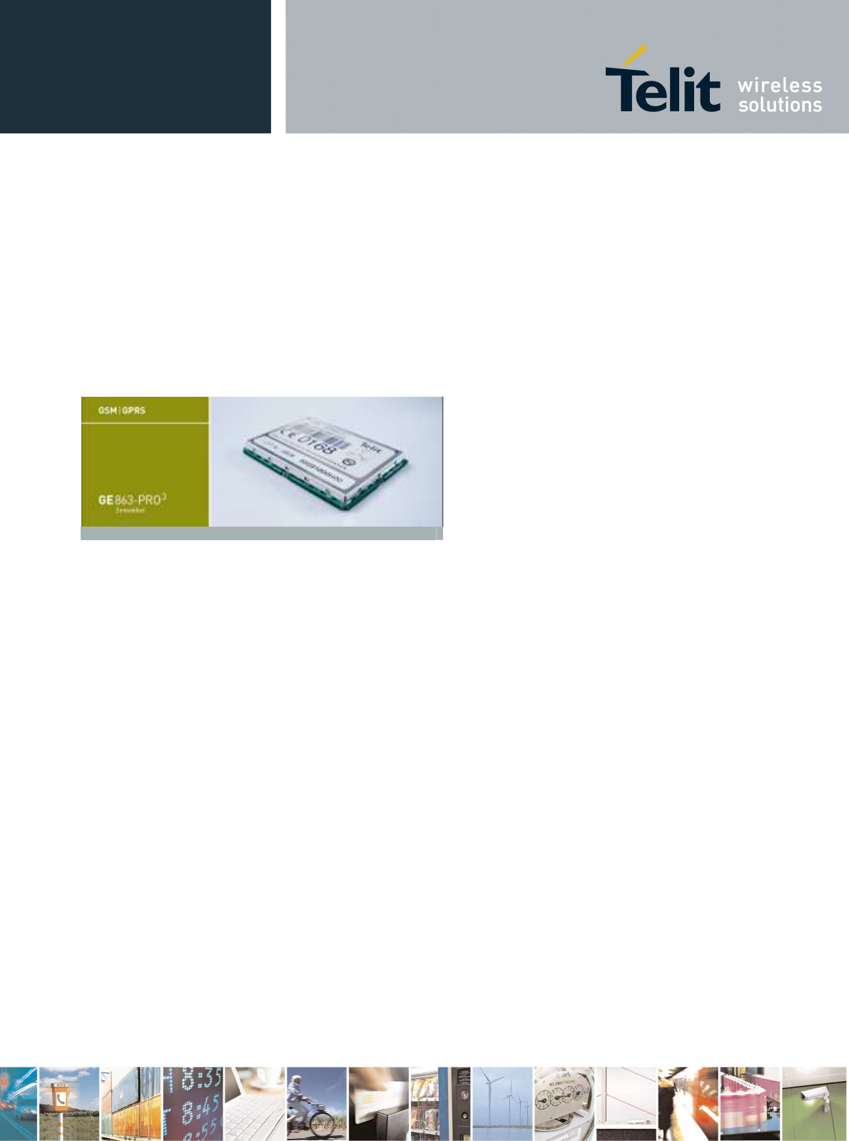
GE863-PRO
3
Product Description
80285ST10036a Rev. 1 DRAFT- 24/04/08
Reproduction forbidden without Telit Communications S.p.A. written authorization - All Rights Reserved page 2 of 53
This document is relating to the following products:
GE863-PRO
3
3 990 250 691

GE863-PRO
3
Product Description
80285ST10036a Rev. 1 DRAFT- 24/04/08
Reproduction forbidden without Telit Communications S.p.A. written authorization - All Rights Reserved page 3 of 53
Contents
1
Overview ...........................................................................................................................7
2
General Product Description.........................................................................................11
2.1 Dimensions ........................................................................................................................ 11
2.2 Weight ................................................................................................................................ 13
2.3 Environmental requirements ............................................................................................ 14
2.3.1
Temperature range .........................................................................................................................14
2.3.2
Vibration Test (non functional)........................................................................................................14
2.3.3
RoHS compliance ...........................................................................................................................14
3
GSM/GPRS Engine.........................................................................................................15
3.1 Operating Frequency......................................................................................................... 15
3.2 Transmitter output power.................................................................................................. 15
3.3 Reference sensitivity......................................................................................................... 15
3.4 Antenna .............................................................................................................................. 16
3.4.1
GSM Antenna .................................................................................................................................16
3.5 Supply voltage................................................................................................................... 16
3.6 Power consumption........................................................................................................... 16
3.7 Embodied Battery charger ................................................................................................ 17
3.8 User Interface..................................................................................................................... 17
3.9 Speech Coding................................................................................................................... 17
3.10 SIM Reader......................................................................................................................... 18
3.11 SMS..................................................................................................................................... 18
3.12 Real Time Clock and Alarm............................................................................................... 18
3.13 Data/fax transmission........................................................................................................ 19
3.14 Local security management.............................................................................................. 19
3.15 Call control......................................................................................................................... 19
3.16 Phonebook......................................................................................................................... 19
3.17 Characters management ................................................................................................... 19
3.18 SIM related functions......................................................................................................... 19
3.19 Call status indication......................................................................................................... 20
3.20 Automatic answer (Voice, Data or FAX)........................................................................... 20
3.21 Supplementary services (SS)............................................................................................ 20

GE863-PRO
3
Product Description
80285ST10036a Rev. 1 DRAFT- 24/04/08
Reproduction forbidden without Telit Communications S.p.A. written authorization - All Rights Reserved page 4 of 53
3.22 Acoustic signalling............................................................................................................ 20
3.23 Buzzer output..................................................................................................................... 21
3.24 RF Transmission Monitor.................................................................................................. 21
3.25 EMC .................................................................................................................................... 21
3.26 Logic level specifications.................................................................................................. 21
3.27 Reset signal ....................................................................................................................... 21
3.28 RTC Bypass out................................................................................................................. 22
3.29 VAUX1 power output ......................................................................................................... 22
3.30 Audio levels specifications............................................................................................... 23
3.31 Software Features.............................................................................................................. 24
3.31.1
Enhanced Easy GPRS Extension ..................................................................................................24
3.31.1.1
Overview .................................................................................................................................24
3.31.1.2
Easy GPRS definition .............................................................................................................25
3.31.2
Multisocket......................................................................................................................................25
3.31.3
Jammed Detect & Report Extension...............................................................................................27
3.31.3.1
Overview .................................................................................................................................27
3.31.4
CMUX .............................................................................................................................................27
3.31.4.1
Product architecture................................................................................................................27
3.31.4.2
Implementation feature and limitation.....................................................................................28
3.31.5
SAP: SIM Access Profile ................................................................................................................29
3.31.5.1
Product architecture................................................................................................................29
3.31.5.2
Implementation feature ...........................................................................................................29
3.31.5.3
Remote SIM Message Command Description .......................................................................29
3.31.6
AT Commands................................................................................................................................30
4
ARM9 Application Engine..............................................................................................31
4.1 General Description........................................................................................................... 31
4.2 Supply voltage................................................................................................................... 31
4.3 Power consumption........................................................................................................... 31
4.4 USARTs .............................................................................................................................. 32
4.5 SPI bus ............................................................................................................................... 32
4.6 Image Sensor Interface ..................................................................................................... 32
4.7 IIC bus ................................................................................................................................ 33
4.8 ISO7816 T0/T1 Interface .................................................................................................... 33
4.9 MultiMedia Card interface ................................................................................................. 33
4.10 Sinchronous Serial Controller .......................................................................................... 33
4.11 Ethernet controller............................................................................................................. 34
4.12 ADC with ADC trigger........................................................................................................ 34

GE863-PRO
3
Product Description
80285ST10036a Rev. 1 DRAFT- 24/04/08
Reproduction forbidden without Telit Communications S.p.A. written authorization - All Rights Reserved page 5 of 53
4.13 DAC Converter................................................................................................................... 34
4.14 USB Device port................................................................................................................. 35
4.15 USB Host port.................................................................................................................... 35
4.16 Clock outputs..................................................................................................................... 35
4.17 GPIO ports.......................................................................................................................... 35
4.18 JTAG Debug Interface....................................................................................................... 36
4.19 Debug UART....................................................................................................................... 36
5
Mounting the GE863-PRO
3
on the Application Board.................................................37
5.1.1
General ...........................................................................................................................................37
5.1.2
Packing system...............................................................................................................................37
6
Evaluation Kit EVK-PRO
3
...............................................................................................40
7
Conformity Assessment Issues....................................................................................41
7.1 GE863-PRO
3
: Conformity Assessment............................................................................. 43
7.2 GE863-PRO
3
: FCC Equipment Authorization................................................................. 45
7.3 GE863- PRO
3
: IC Equipment Authorization..................................................................... 46
7.4 GE863-PRO
3
: RoHS certificate.......................................................................................... 47
8
Safety Recommandations .............................................................................................48
9
GE863-PRO
3
Technical Support....................................................................................49
10
List of acronyms.............................................................................................................50
11
Document Change Log..................................................................................................53

GE863-PRO
3
Product Description
80285ST10036a Rev. 1 DRAFT- 24/04/08
Reproduction forbidden without Telit Communications S.p.A. written authorization - All Rights Reserved page 6 of 53
DISCLAIMER
The information contained in this document is proprietary information of Telit Communications S.p.A.
and its affiliates (“TELIT”). The contents are confidential and any disclosure to persons other than the
officers, employees, agents or subcontractors of the owner or licensee of this document, without the
prior written consent of Telit, is strictly prohibited.
Telit makes every effort to ensure the quality of the information it makes available. Notwithstanding the
foregoing, Telit does not make any warranty as to the information contained herein, and does not
accept any liability for any injury, loss or damage of any kind incurred by use of or reliance upon the
information.
Telit disclaims any and all responsibility for the application of the devices characterized in this
document, and notes that the application of the device must comply with the safety standards of the
applicable country, and where applicable, with the relevant wiring rules.
Telit reserves the right to make modifications, additions and deletions to this document due to
typographical errors, inaccurate information, or improvements to programs and/or equipment at any
time and without notice. Such changes will, nevertheless be incorporated into new editions of this
document.
All rights reserved.
© 2007 Telit Communications S.p.A.
GE863-PRO
3
Product Description
80285ST10036a Rev. 1 DRAFT- 24/04/08
Reproduction forbidden without Telit Communications S.p.A. written authorization - All Rights Reserved page 7 of 53
1 Overview
The GE863-PRO
3
is the Telit latest product generation deriving from the top reliable BGA GE863
product family now including a quad-band GSM/GPRS class 10 engine as well as a dedicated ARM9
application processor (the ATMEL standard microcontroller AT91SAM9260) and FLASH & RAM
memories.
Managemen
t
Power
8MB
SDRAM
4MB
SPI
FLASH
Management
Power
GSM Radio
Antenna Conn.
Ball Grid Array
Bus
Data
SPI
Bus
internal 32KHz
RC
ARM9 AT91SAM9260
Peripherals
Processor
GSM/GPRS Baseband
Oscillator
6 MHz
26MHz
Crystal
32 KHz
Crystal
External Interconnections between ARM processor and GSM/GPRS baseband
Supply ARM Supply GSM
G
GE
E8
86
63
3-
-P
PR
RO
O
3
3

GE863-PRO
3
Product Description
80285ST10036a Rev. 1 DRAFT- 24/04/08
Reproduction forbidden without Telit Communications S.p.A. written authorization - All Rights Reserved page 8 of 53
This innovative dual core architecture allows one consistent product for all global GSM networks that
is also capable of managing complex and demanding customer applications, giving impressive
advantages in terms of
final application time-to-market
final application cost reduction by saving R&D, approvals & certifications, logistic & production
costs
production yield by BoM part count reduction
optimization of final application total cost of ownership (increased reliability of integrated
architecture compared to the discrete one)
final application overall dimension (exploiting the compact telit design)
The proven unique Telit Ball-Grid-Array (BGA) package concept enables a very low profile and a small
product size to design extremely compact applications using location technology. Since all connectors
are eliminated, the solution cost is significantly reduced compared to conventional mounting concepts.
Furthermore thanks to the successful cooperation with ATMEL, the dimensions of the ARM package
have been considerably decreased so that our clients can reduce the dimensions of the entire system
that integrates GPRS, the additional processor and the memories, giving a competitive advantage in
comparison to a non integrated architecture and maintaining at the same time the flexibility of a
standard ATMEL ARM9 product (AT91SAM9260)
With its low profile design and extended programming capabilities in C++ and/or Python, fast ROM
and RAM plus power management, 4MB serial flash (expandible) and 8MB SDRAM (standard)
expandable up to 64MB for custom designs, the Telit GE863-PRO
3
is the perfect and complete
hardware platform for all compact complex and individual customer solutions.
Interfaces such as SPI, IIC, SD/MMC and USB give connectivity to external peripherals (camera,
keyboard, display), complementary short range wireless technologies (Wi-Fi, Bluetooth, ZigBee) and
position location technology (GPS) for which Telit can offer you complete reference designs.
The ARM core also includes real-time OS (LINUX), multitasking and fully available 200MIPS,
fundamental for complex and demanding real-time applications. However Telit can also provide
products without operating system giving with these an unlimited possibility for clients who want to use
their own system environment on our modules.
As a part of Telit’s corporate policy of environmental protection, all products comply to the RoHS
(Restriction of Hazardous Substances) directive of the European Union (EU Directive 2002/95/EG).
Other than the above mentioned features, the Telit dual-core GE863-PRO
3
maintains the following
functionalities:
• EASY GPRS (AT driven embedded TCP/IP protocol stack, including FTP client)
• EASY SCAN (full GSM frequency scanning)
• JAMMING DETECT & REPORT (detect the presence of disturbing devices)

GE863-PRO
3
Product Description
80285ST10036a Rev. 1 DRAFT- 24/04/08
Reproduction forbidden without Telit Communications S.p.A. written authorization - All Rights Reserved page 9 of 53
• CMUX
• SAP (SIM Access Profile)
• Multisocket
From the interface point of view, the GE863-PRO
3
provides the following:
• 1 Full GSM engine RS232 UART, CMOS level (ASC0) interface for AT commands:
- Auto-bauding from 2.4 up to 57.6 Kbps
- Fixed baud rate up to 115.2 Kbps
• 1 FULL ARM9 RS232 USART, CMOS level (UART0) interface for AT command drive
• 3 Four wires ARM9 RS232 USART, CMOS level
• 2 Two wires ARM9 RS232 UART, CMOS level
• 2 ARM9 SPI interfaces for up to 18 slaves
• 1 ARM9 Image Sensor Interface ITU-B 601/656
• 1 ARM9 IIC bus
• 1 ARM9 ISO7816 T0/T1 SAM/Smartcard interface
• 1 ARM9 SD/MMC Multimedia Card Interface
• 1 ARM9 Synchronous Serial Controller ( I2S ) interface for digital audio
• 1 ARM9 Ethernet controller
• 4 ARM9 ADC with ADC trigger input
• 6 ARM9 DAC (PWM)
• 1 ARM9 USB Device port
• 2 ARM9 USB Host port
• 2 ARM9 clock output pins
• 1 ARM9 Debug Trace Serial port
• 1 ARM9 JTAG debug port
• 2 analog GSM audio path
• SIM card interface, 3 volts and 1.8 volts
• 90 ARM9 + 9 GSM GPIO ports (max)
• 1 GSM buzzer output
• 1 GSM alarm output
• 1 GSM led status output indicator
In order to meet the competitive OEM and vertical market stringent requirements, Telit supports its
customers with a dedicated Technical Support Policy with:
• Telit GE863-PRO
3
Evaluation Kit to help you to develop your application;
• a Website with all updated information available;

GE863-PRO
3
Product Description
80285ST10036a Rev. 1 DRAFT- 24/04/08
Reproduction forbidden without Telit Communications S.p.A. written authorization - All Rights Reserved page 10 of 53
• a high level technical support to assist you in your development;
For more updated information concerning product Roadmap and availability, technical characteristics,
commercial and other issues, please check on the Telit website www.telit.com > Products > Modules.
NOTE: Some of the performances of the Telit GE863-PRO
3
modules depend on the SW version
installed on the module itself.
The Telit GE863-PRO
3
SW group is continuously working in order to add new features and improve
the overall performances.
The Telit GE863-PRO
3
modules are easily upgradeable by the developer using the Telit GE863-
PRO
3
module Flash Programmer.

GE863-PRO
3
Product Description
80285ST10036a Rev. 1 DRAFT- 24/04/08
Reproduction forbidden without Telit Communications S.p.A. written authorization - All Rights Reserved page 11 of 53
2 General Product Description
The Telit GE863-PRO
3
module includes the GSM/GPRS engine plus a dedicated ARM9 application
processor and memories.
The two processors [GSM/GPRS engine & Application processor] are kept as much as possible
distinct: they have different power sources but with the same voltage range, so that, either power
management can be optimized, by splitting GSM and application supplies, or cost can be optimized,
by using the same power source to supply the two parts.
Furthermore in order to give the maximum flexibility the two engines can be operated independently
each other.
NOTE: The illustrations in this Product Description are only schematic and do not assure fidelity to
construction or layout details, finishes, writings or colors.
2.1 Dimensions
The Telit GE863-PRO
3
module overall dimensions are:
• Length: 41,4 mm
• Width: 31,4 mm
• Thickness: 3,6 mm
The layout of the Telit GE863-PRO
3
module is shown in the following figure:
GE863-PRO
3
Product Description
80285ST10036a Rev. 1 DRAFT- 24/04/08
Reproduction forbidden without Telit Communications S.p.A. written authorization - All Rights Reserved page 12 of 53
Top View
GE863-PRO
3
Product Description
80285ST10036a Rev. 1 DRAFT- 24/04/08
Reproduction forbidden without Telit Communications S.p.A. written authorization - All Rights Reserved page 13 of 53
Bottom View
2.2 Weight
The Telit GE863-PRO
3
module weight is 9 gr.

GE863-PRO
3
Product Description
80285ST10036a Rev. 1 DRAFT- 24/04/08
Reproduction forbidden without Telit Communications S.p.A. written authorization - All Rights Reserved page 14 of 53
2.3 Environmental requirements
The Telit GE863-PRO
3
module is compliant to the applicable ETSI reference documentation GSM 05.05
Release1998.
2.3.1 Temperature range
GE863-PRO
3
Temperature in normal operating conditions –10°C ÷ +55°C
Temperature in extreme operating conditions* –35°C ÷ +85°C
(TBD)
Temperature in not functional conditions –40°C ÷ +85°C
* Temperature exceeding the range of normal functional conditions can affect the sensitivity, the performance and the
MTBF of the module.
2.3.2 Vibration Test (non functional)
• 10 ÷12Hz ASD = 1.92m 2 /s 3
• 12 ÷ 150Hz –3dB/oct
2.3.3 RoHS compliance
The Telit GE863-PRO
3
module family is fully compliant to EU regulation on RoHS.
GE863-PRO
3
Product Description
80285ST10036a Rev. 1 DRAFT- 24/04/08
Reproduction forbidden without Telit Communications S.p.A. written authorization - All Rights Reserved page 15 of 53
3 GSM/GPRS Engine
3.1 Operating Frequency
The operating frequencies in GSM, DCS, PCS modes are conform to the GSM specifications.
Mode Freq. TX (MHz) Freq. RX (MHz) Channels (ARFC)
TX - RX offset
E-GSM-900
890.0 - 914.8 935.0 - 959.8 0 – 124 45 MHz
880.2 - 889.8 925.2 - 934.8 975 - 1023 45MHz
GSM-850 824.2 - 848.8 869.2 - 893.8 128 - 251 45 MHz
DCS-1800 1710.2 - 1784.8 1805.2 - 1879.8 512 – 885 95 MHz
PCS-1900 1850.2 - 1909.8 1930.2 - 1989.8 512 - 810 80 MHz
3.2 Transmitter output power
GSM–850 / 900
The Telit GE863-PRO
3
modules in GSM–850 / 900 operating mode are of class 4 in accordance with the
specification which determine the nominal 2W peak RF power (+33dBm) on 50 Ohm.
DCS–1800 / PCS–1900
The Telit GE863-PRO
3
modules in DCS–1800/PCS–1900 operating mode are of class 1 in accordance
with the specifications, which determine the nominal 1W peak RF power (+30dBm) on 50 Ohm.
3.3 Reference sensitivity
GSM–850 / 900
The sensitivity of the Telit GE863-PRO
3
modules according to the specifications for the class 4 GSM–
850/900 portable terminals is –107 dBm typical in normal operating conditions.
DCS–1800 / PCS-1900
GE863-PRO
3
Product Description
80285ST10036a Rev. 1 DRAFT- 24/04/08
Reproduction forbidden without Telit Communications S.p.A. written authorization - All Rights Reserved page 16 of 53
The sensitivity of the Telit GE863-PRO
3
modules according to the specifications for the class 1 portable
terminals DCS-1800 / PCS-1900 is –106 dBm typical in normal operating conditions.
3.4 Antenna
3.4.1 GSM Antenna
The antenna that the customer chooses to use, should fulfill the following requirements:
Frequency range Depending by frequency band(s) provided by the network operator,
the customer shall use the most suitable antenna for that/those
band(s).
Bandwidth 70 MHz in GSM 850, 80 MHz in GSM 900, 170 MHz in DCS, 140 MHz
PCS band
For further information please refer to the GE863-PRO
3
Hardware User Guide.
3.5 Supply voltage
The external power supply must be connected to VBATT signal pin (see Hardware User Guide) and
must fulfill the following requirements:
Nominal operating voltage 3.8 V
Operating voltage range 3.4 V – 4.2 V
Absolute Minimum voltage 3.30V
Absolute Maximum voltage 4.50 V
NOTE: Operating voltage range must never be exceeded; care must be taken in order to fulfill
absolute min/max voltage requirements.
3.6 Power consumption
The typical current consumption of the GSM/GPRS part of the Telit GE863-PRO
3
module is:
Power off current (typical) < 28 µA;
Stand–by current (GSM Idle) < 17 mA (< 4 mA using command AT+CFUN)
Operating current in voice channel < 200 mA @ worst network conditions
Operating current in GPRS class 10
< 370 mA @ worst network conditions
GE863-PRO
3
Product Description
80285ST10036a Rev. 1 DRAFT- 24/04/08
Reproduction forbidden without Telit Communications S.p.A. written authorization - All Rights Reserved page 17 of 53
The total power consumption of GE863-PRO
3
is the sum of the consumptions of GSM and ARM9
processor part.
3.7 Embodied Battery charger
The battery charger is suited for a 3.7V Li-Ion rechargeable battery (suggested capacity 500-
1000mAh). The Charger needs only a CURRENT LIMITED power source input and charges the
battery directly through VBATT connector pins.
Battery charger input pin CHARGE
Battery pins VBATT, GND
Battery charger input voltage min 5.0 V
Battery charger input voltage typical 5.5 V
Battery charger input voltage max 7.0 V
Battery charger input current max 400mA
Battery type Li-Ion rechargeable
NOTE: If embodied battery charger is used, then a LOW ESR capacitor of at least 100µF must be
mounted in parallel to VBATT pin.
NOTE: when power is supplied to the CHARGE pin, a battery must always be connected to the
VBATT pins of the GE863-PRO
3
.
3.8 User Interface
The user interface of the Telit GE863-PRO
3
GSM/GPRS engine is managed by AT commands specified
on the ITU-T V.250, GSM 07.07 and GSM 07.05 specifications.
3.9 Speech Coding
The Telit GE863-PRO
3
modules voice codec supports the following rates:
• Half Rate
• Full rate
• Enhanced Full Rate
• Adaptive Multi Rate

GE863-PRO
3
Product Description
80285ST10036a Rev. 1 DRAFT- 24/04/08
Reproduction forbidden without Telit Communications S.p.A. written authorization - All Rights Reserved page 18 of 53
3.10 SIM Reader
The Telit GE863-PRO
3
modules support phase 2 GSM11.14 - SIM 1.8V and 3V. For 5V SIM cards, an
external level translator can be added. All models need an external SIM card holder.
3.11 SMS
The Telit GE863-PRO
3
modules support the following SMS types, in text and PDU mode:
• Mobile Terminated (MT) class 0 – 3 with signaling of new incoming SMS, SIM full, SMS read
• Mobile Originated class 0 – 3 with writing, memorize in SIM and sending
• Cell broadcast compatible with CB DRX with signaling of new incoming SMS.
3.12 Real Time Clock and Alarm
The Telit GE863-PRO
3
modules GSM/GPRS engine support the Real Time Clock and Alarm functions
through AT commands; furthermore anyone of the GSM/GPRS GPIO available can be configured as
alarm output pin to indicate the alarm with a hardware line output.
The Voltage Output of the RTC power supply is provided on a pin so that a backup capacitor can be
added to increase the RTC autonomy.

GE863-PRO
3
Product Description
80285ST10036a Rev. 1 DRAFT- 24/04/08
Reproduction forbidden without Telit Communications S.p.A. written authorization - All Rights Reserved page 19 of 53
3.13 Data/fax transmission
The Telit GE863-PRO
3
modules support:
• Packed Data transfer GPRS Class 10, Multi-slot Class B
• CSD up to 14.4 Kbps
• Fax service, Class 1 Group 3
3.14 Local security management
The local security management can be done with the lock of Subscriber Identity module (SIM), and
security code request at power–up.
3.15 Call control
The call cost control function is supported.
3.16 Phonebook
This function allows storing of the telephone numbers in SIM memory. The capability depends on SIM
version and embedded memory.
3.17 Characters management
The Telit GE863-PRO
3
modules support the IRA character set (International Reference Alphabet), in
TEXT mode and IRA/UCS2/GSM/ISO-8859-1/PCCP437 in PDU mode.
3.18 SIM related functions
The activation and deactivation of the numbers stored in phone book, FDN, ADN and PINs are
supported. The extension at the PIN2 for the PUK2 insertion capability for lock condition is supported
too.

GE863-PRO
3
Product Description
80285ST10036a Rev. 1 DRAFT- 24/04/08
Reproduction forbidden without Telit Communications S.p.A. written authorization - All Rights Reserved page 20 of 53
3.19 Call status indication
The call status indication by AT commands is supported.
3.20 Automatic answer (Voice, Data or FAX)
After a specified number of rings, the module will automatically answer. The user can set the number
of rings by means of the command ATS0=<n>.
3.21 Supplementary services (SS)
The following supplementary services are supported:
• Call Barring,
• Call Forwarding,
• Calling Line Identification Presentation (CLIP),
• Calling Line Identification Restriction (CLIR),
• Call Waiting, other party call Waiting Indication,
• Call Hold, other party Hold / Retrieved Indication,
• Closed User Group supplementary service (CUG),
• Advice of Charge,
• Unstructured SS Mobile Originated (MO)
3.22 Acoustic signalling
The acoustic signals of Telit GE863-PRO
3
modules on the selected acoustic device are the following:
• Call waiting;
• Ringing tone;
• SMS received tone;
• Busy tone;
• Power on/off tone;
• Off Hook dial tone;
• Congestion tone;
• Connected tone;
• Call dropped;
• No service tone;
• Alarm tone.

GE863-PRO
3
Product Description
80285ST10036a Rev. 1 DRAFT- 24/04/08
Reproduction forbidden without Telit Communications S.p.A. written authorization - All Rights Reserved page 21 of 53
3.23 Buzzer output
The General Purpose I/O pin GPIO7 can be configured to output the BUZZER output signal, with only
an external MOSFET/transistor and a diode a Buzzer can be directly driven.
The ringing tone and the other signaling tones can be redirected to this Buzzer output with a specific
AT command.
3.24 RF Transmission Monitor
As alternate function of the GPIO5, the GE863-PRO
3
provide the RF transmission monitor. When the
alternate function is activated, the pin of GPIO5 changes to HIGH every time the module transmits an
RF signal and remains HIGH for the duration of the transmission sequence, i.e. it does not change
with every GSM signal burst.
3.25 EMC
Compliant to EN301-489-1 and EN301-489-7 and all applicable GSM Specifications. Compliant to
Directive 1999/05/CE.
3.26 Logic level specifications
Where not specifically stated, all the interface circuits of the GSM/GPRS engine work at 2.8V CMOS
logic levels. To get more detailed information about the logic level specifications used in the Telit
GE863-PRO
3
interface circuits please consult the Hardware User Guide.
3.27 Reset signal
The RESET is used to reset the GSM/GPRS engine of the Telit GE863-PRO
3
modules. Whenever this
signal is pulled low, the GSM/GPRS engine is rebooted. When the device is reset it stops any
operation. After the release of the reset the GSM/GPRS engine is unconditionally rebooted, without
doing any detach operation from the network where it is registered to. This behavior is not like a
proper shut down because any GSM device is requested to issue a detach request on turn off. For this
reason the Reset signal must be used only as an emergency exit in the rare case the device remains
stucked waiting for some network response.
GE863-PRO
3
Product Description
80285ST10036a Rev. 1 DRAFT- 24/04/08
Reproduction forbidden without Telit Communications S.p.A. written authorization - All Rights Reserved page 22 of 53
NOTE: do not use this signal to power off the Telit GE863-PRO
3
module. Use the ON/OFF signal to
perform this function or the AT#SHDN command.
3.28 RTC Bypass out
The VRTC pin brings out the Real Time Clock supply, which is separate from the rest of the digital
part, allowing having only RTC going on when all the other parts of the device are off.
To this power output a backup capacitor can be added in order to increase the RTC autonomy during
power off of the battery. NO Devices must be powered from this pin.
3.29 VAUX1 power output
A regulated power supply output is provided in order to supply small devices from the module.
This output is active when the module is ON and goes OFF when the module is shut down.
The operating range characteristics of the supply are:
Operating Range – VAUX1 power supply
Min Typical Max
Output voltage 2.75V 2.85V 2.95V
Output current 100mA / 50mA
Output bypass capacitor
2.2µF

GE863-PRO
3
Product Description
80285ST10036a Rev. 1 DRAFT- 24/04/08
Reproduction forbidden without Telit Communications S.p.A. written authorization - All Rights Reserved page 23 of 53
3.30 Audio levels specifications
The audio of the Telit GE863-PRO
3
modules is organized into two main paths:
• Internal path (called also MT)
• External path (called also HF)
These two paths are meant respectively for handset and headset/hands-free use.
The Telit GE863-PRO
3
modules have a built in echo canceller and a noise suppressor, tuned separately
for the two audio paths; for the internal path the echo canceller parameters are suited to cancel the
echo generated by a handset, while for the external audio path they are suited for a hands-free use.
For more information on the audio refer to the GE863-PRO
3
Hardware User Guide.
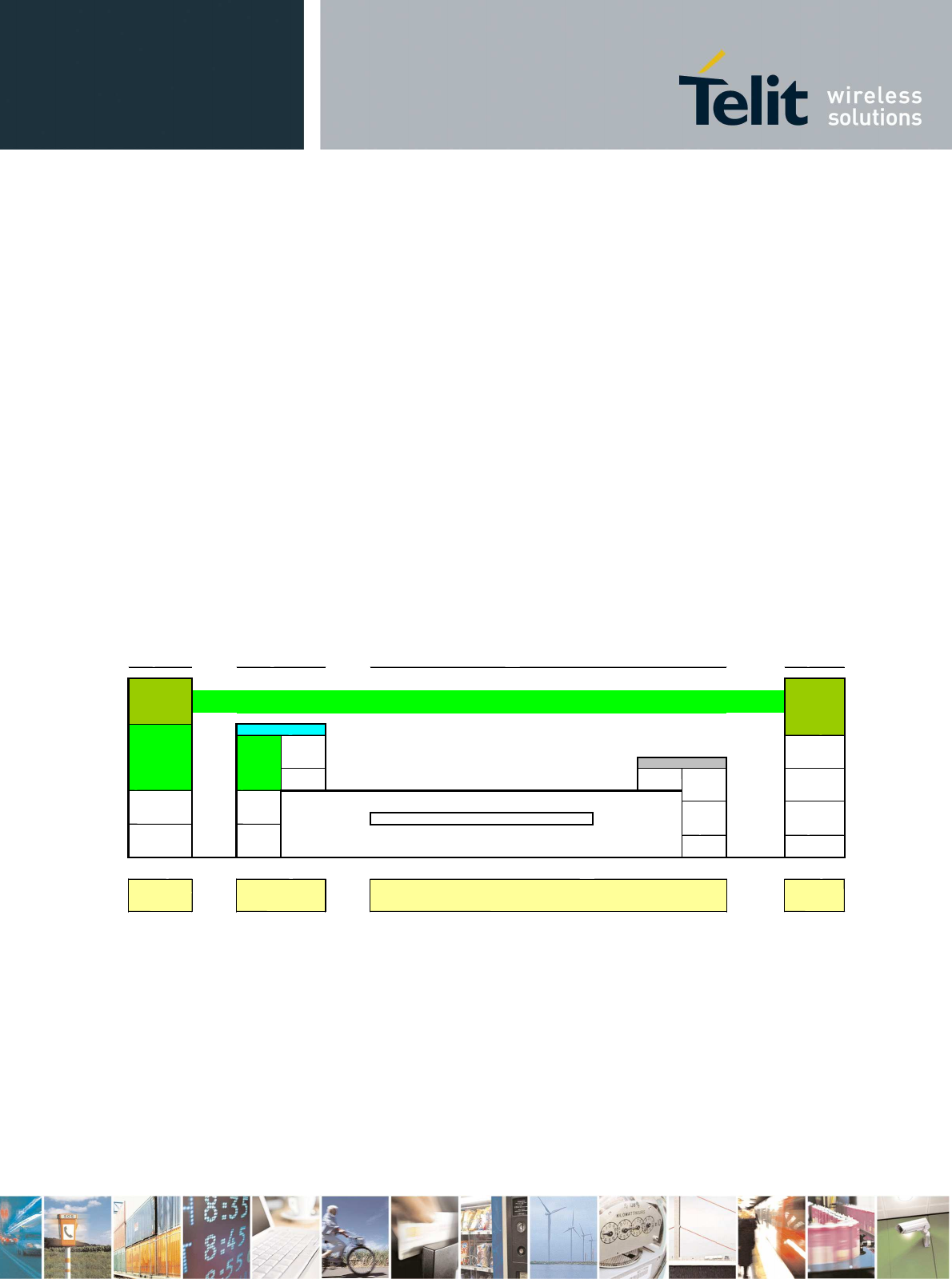
GE863-PRO
3
Product Description
80285ST10036a Rev. 1 DRAFT- 24/04/08
Reproduction forbidden without Telit Communications S.p.A. written authorization - All Rights Reserved page 24 of 53
3.31 Software Features
3.31.1 Enhanced Easy GPRS Extension
3.31.1.1 Overview
The Easy GPRS feature allows a Telit GE863-PRO
3
modules user to contact a device in Internet and
establish with it a raw data flow over the GPRS and Internet networks.
This feature can be seen as a way to obtain a “virtual” serial connection between the Application
Software on the Internet machine involved and the controller of the Telit GE863-PRO
3
modules,
regardless of all the software stacks underlying.
An example of the protocol stack involved in the devices is reported:
This particular implementation allows to the devices interfacing to the Telit GE863-PRO
3
modules the use
of the GPRS and Internet packet service without the need to have an internal TCP/IP stack since this
function is embedded inside the module.
Easy GPRS overcomes some of the known limitations of the previous implementation and implements
some new features such as:
• Keep the GPRS context active even after the closing of a socket, allowing the application to keep
the same IP address;
• Also Mobile terminated (incoming) connections can be made, now it is possible to receive
incoming TCP connection requests;
Remot
e
Controlle
r
Device
Device
(Internet)
Local
Remot
e
Applicatio
n
Applicatio
n
TCP/UD
P
EAS
Y
EAS
Y
TCP/UD
P
GPR
S
GPR
S
IP
IP IP IP
Serial
Data
Line
o
n
Driver
Board
L2
L2
V.24 V.24
L1
L1
Termina
l
Equipmen
t
Remot
e
Device
(Internet)
network
interworking
Mobile
Terminal
GPRS Network and
Internet
Teli
t
GE863
networks
<<<---------------------------------- Virtual Serial link ---------------------------------->>>

GE863-PRO
3
Product Description
80285ST10036a Rev. 1 DRAFT- 24/04/08
Reproduction forbidden without Telit Communications S.p.A. written authorization - All Rights Reserved page 25 of 53
• A new internal firewall has been implemented in order to guarantee a certain level of security on
internet applications.
3.31.1.2 Easy GPRS definition
The Easy GPRS feature provides a way to replace the need of an Internet TCP/IP stack at the
terminal equipment side. The steps that will be required to obtain a virtual serial connection (that is
actually a socket) to the Internet peer are:
• Configuring the GPRS Access
• Configuring the embedded TCP/IP stack behavior
• Defining the Internet Peer to be contacted
• Request the GPRS and socket connections to be opened (host is connected)
• Exchange raw data
• Close the socket and GPRS context
All these steps are achieved through AT commands.
As for common modem interface, two logical statuses are involved: command mode and data traffic
mode:
• In Command Mode (CM), some AT commands are provided to configure the Data Module
Internet stack and to start up the data traffic.
• In data traffic mode (Socket Mode, SKTM), the client can send/receive a raw data stream
which will be encapsulated in the previously configured TCP / IP packets which will be sent to
the other side of the network and vice versa. Control plane of ongoing socket connection is
deployed internally to the module.
For more detailed information regarding GPRS please consult Easy GPRS User Guide and AT
Commands Reference Guide.
3.31.2 Multisocket
New functionality of the Telit modules, multisocket is an extension of Telit Easy GPRS feature, which
allows the user to have two contexts activated (that means two different IP address), more than one
socket connection (with a maximum of 6) and simultaneous FTP client service.
The basic idea of multisocket is the possibility of suspend a socket connection with the escape
sequence +++.
With IP Easy we can use a SKTD to open a socket connection and go online. After online activities we
use +++ sequence to close the connection (see the figure below).
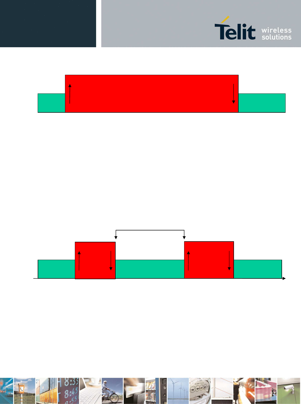
GE863-PRO
3
Product Description
80285ST10036a Rev. 1 DRAFT- 24/04/08
Reproduction forbidden without Telit Communications S.p.A. written authorization - All Rights Reserved page 26 of 53
Where the green part represents the module command mode while the red part is the online mode.
Now, the online mode can be suspended with the escape sequence by using the multisocket feature.
During suspend mode the data received by the socket will be buffered. These data will be displayed
after socket resumption, as shown in the figure below:
This new feature allows the user to switch between online mode and command mode without closing
the connection and eventually opening another socket (or resuming the suspended one) or FTP
connection.
Another feature is the possibility to associate any socket connection to a specific context, this means
that we can use different IP addresses for the connections (max 2). Socket identifier is called
Connection Id (selects which socket we want to use from 1 up to 6) and every Connection Id is
associated to a context.
For more detailed information please consult Multisocket User Guide.
On Line +++
Online mode
Data Traffic
On Line Suspend On Line Suspend
Data
Data
Socket is still alive

GE863-PRO
3
Product Description
80285ST10036a Rev. 1 DRAFT- 24/04/08
Reproduction forbidden without Telit Communications S.p.A. written authorization - All Rights Reserved page 27 of 53
3.31.3 Jammed Detect & Report Extension
3.31.3.1 Overview
The Jammed Detect & Report feature allows a Telit GE863-PRO
3
module to detect the presence of a
disturbing device such as a Communication Jammer and give indication to the user and/or send a
report of that to the network.
This feature can be very important in alarm, security and safety applications that rely on the module
for the communications. In these applications, the presence of a Jammer device can compromise the
whole system reliability and functionality and therefore shall be recognized and reported either to the
local system for countermeasure actions or to the network providing remote actions.
An example scenario could be an intrusion detection system that uses the module for sending the
alarm indication for example with an SMS to the system owner, and thief incomes using a Jammer to
prevent any communication between the GSM module and the network.
In such a case, the module detects the Jammer presence even before the break in and can trigger an
alarm siren, other communication devices (PSTN modem) or directly report this condition to the
network that can provide further security services for example sending SMS to the owner or police.
Obviously this last service depends also from network infrastructure support and it may not be
supported by some networks.
3.31.4 CMUX
CMUX ( Converter-Multiplexer) is a multiplexing protocol implemented in the Telit module that can be
used to send any data, SMS, fax, TCP data.
3.31.4.1 Product architecture
The Multiplexer mode enables one serial interface to transmit data to four different customer
applications. This is achieved by providing four virtual channels using a Multiplexer (Mux).
This is especially advantageous when a fax/data/GPRS call is ongoing. Using the Multiplexer features,
e.g. controlling the module or using the SMS service can be done via the additional channels without
disturbing the data flow; access to the second UART is not necessary.
Furthermore, several accesses to the module can be created with the Multiplexer. This is of great
advantage when several independent electronic devices or interfaces are used.

GE863-PRO
3
Product Description
80285ST10036a Rev. 1 DRAFT- 24/04/08
Reproduction forbidden without Telit Communications S.p.A. written authorization - All Rights Reserved page 28 of 53
To access the three virtual interfaces, both the GSM engine and the customer application must
contain Mux components, which communicate over the multiplexer protocol.
In Multiplexer mode, AT commands and data are encapsulated into packets. Each packet has channel
identification and may vary in length.
3.31.4.2 Implementation feature and limitation
• 7.10 CMUX Basic Option used
• CMUX implementation support four full DLCI (Serial Port)
• CMUX can operate only at Fixed rate, if AT+CMUX is sent with IPR=0 an Error is returned,
with a maximum rate of 115200
• Every instance has its own user profile storage in NVM
• Independent setting of unsolicited message.
• In case of GPS product one serial port can be dedicated to NMEA output.
• Every Instance has its own independent flow control.
NOTE: More details about the Multiplexer mode are available in the Cmux User Guide.

GE863-PRO
3
Product Description
80285ST10036a Rev. 1 DRAFT- 24/04/08
Reproduction forbidden without Telit Communications S.p.A. written authorization - All Rights Reserved page 29 of 53
3.31.5 SAP: SIM Access Profile
3.31.5.1 Product architecture
The SAP feature allow the module to use the SIM of a remote SIM Server. This feature is
implemented using special AT Command on a Virtual circuit of the CMUX interface.
3.31.5.2 Implementation feature
• SAP is based on 7.10 CMUX Basic Option used
• Only SAP Client features
• Logic HW flow control is recommended on the Virtual instance selected for the SAP command.
3.31.5.3 Remote SIM Message Command Description
The module sends request commands to the client application through a binary message that is
crowned in the CMUX message. The client application shall extract the message and send it to the
SAP server, through the appropriate protocols (e.g. by RFCOMM, that is the Bluetooth serial port
emulation entity).
The client application shall extract all the messages sent by SAP server and put them in the CMUX
message, to sent to the module.
The module satisfies the following feature requirements:
• Connection management
• Transfer APDU
• Transfer ATR
• Power SIM on
• Report Status
• Error Handling
Every feature needs some procedures support:
Feature Procedure
Connect
Report Status
Transfer ATR
Disconnection Initiated by the Client
Connection Management
Disconnection Initiated by the Server
Transfer APDU Transfer APDU
Transfer ATR Transfer ATR
Power SIM on Power SIM on

GE863-PRO
3
Product Description
80285ST10036a Rev. 1 DRAFT- 24/04/08
Reproduction forbidden without Telit Communications S.p.A. written authorization - All Rights Reserved page 30 of 53
Transfer ATR
Report Status Report Status
Error Handling Error Response
Report Status, Disconnection Initiated by the Server and Error Response are independent messages
sent by server. The other procedures consist of couples of messages, started by client.
NOTE: More details about the SAP are available in the SAP User Guide.
3.31.6 AT Commands
The Telit GE863-PRO
3
modules can be driven via the serial interface using the standard AT commands
1
.
The Telit GE863-PRO
3
modules are compliant with:
• Hayes standard AT command set, in order to maintain the compatibility with existing SW
programs.
• ETSI GSM 07.07 specific AT command and GPRS specific commands.
• ETSI GSM 07.05 specific AT commands for SMS (Short Message Service) and CBS (Cell
Broadcast Service)
• FAX Class 1 compatible commands
Moreover the Telit GE863-PRO
3
modules support also Telit proprietary AT commands for special
purposes.
For a detailed description of GE863 modules AT Commands refer to document AT Commands
Reference Guide, code 80000ST10025a.
1
The AT is an ATTENTION command and is used as a prefix to other parameters in a string. The AT
command combined with other parameters can be set up in the communications package or typed in
manually as a command line instruction.

GE863-PRO
3
Product Description
80285ST10036a Rev. 1 DRAFT- 24/04/08
Reproduction forbidden without Telit Communications S.p.A. written authorization - All Rights Reserved page 31 of 53
4 ARM9 Application Engine
4.1 General Description
The Application engine is an ATMEL AT91SAM9260 and comprises an ARM926EJ-S processor with
fast ROM and RAM plus power management and 8Mbyte SDRAM 100MHz and a 4Mbyte serial flash.
The ARM926EJ-S has a full set of peripherals ranging from several USART to the USB Host
controller, allowing almost any connectivity to be achieved.
The ARM has two clock sources, a 6MHz crystal oscillator clock source providing the main clock that
can be multiplied up to 200MHz and the internal RC slow clock source providing 32KHz. If more
accuracy in the 32KHz clock is needed, then an external 32KHz crystal can be added.
4.2 Supply voltage
The external power supply must be connected to VBATT2 signal pin (see Hardware User Guide) and
must fulfill the following requirements:
Nominal operating voltage 3.8 V
Operating voltage range 3.4 V – 4.2 V
Absolute Minimum voltage 3.30V
Absolute Maximum voltage 4.50 V
NOTE: Operating voltage range must never be exceeded; care must be taken in order to fulfill
absolute min/max voltage requirements.
4.3 Power consumption
The typical current consumption of the ARM9 part of the Telit GE863-PRO
3
module is:
Power off current (typical) < 1.5 µA
Stand–by current @ slow clocking 1 mA [ TBD ]
Operating current typical @ 200MHz 140 mA [ TBD ]
The total power consumption of GE863-PRO
3
is the sum of the consumptions of GSM and ARM9
processor part.

GE863-PRO
3
Product Description
80285ST10036a Rev. 1 DRAFT- 24/04/08
Reproduction forbidden without Telit Communications S.p.A. written authorization - All Rights Reserved page 32 of 53
4.4 USARTs
The Application processor has 1 Full (9 wires) RS232 USART , 3 USART with Hardware Flow
Control, 2 two wire UARTs.
4.5 SPI bus
The Application processor has 2 set of Serial Peripheral Interfaces buses, SPI0 and SPI1. Each of
these SPI bus has four Chip Select lines, that can be encoded to provide access to 15 peripherals
[with external CS decoding].
The CS1 of the SPI0 bus is internally connected to the Serial Flash, hence SPI0 cannot use encoded
CS and therefore only 3 other devices can be connected to the SPI0 interface. SPI1 bus can use the
encoding.
The SPI busses support Master, Multiple Master or Slave mode.
The SPI bus consists of two data lines and two control lines:
• Master Out Slave In (MOSI): This data line supplies the output data from the master shifted into the
input(s) of the slave(s).
• Master In Slave Out (MISO): This data line supplies the output data from a slave to the input of the
master. There may be no more than one slave transmitting data during any particular transfer.
• Serial Clock (SPCK): This control line is driven by the master and regulates the flow of the data bits.
The master may transmit data at a variety of baud rates; the SPCK line cycles once for each bit that is
transmitted.
• Chip Select (NPCS): This control line allows slaves to be turned on and off by hardware.
All combinations of Clock Polarity (CPOL) and Clock Phase (CPHA) is supported by the bus.
4.6 Image Sensor Interface
The Image Sensor Interface (ISI) connects a CMOS-type image sensor to the processor and provides
image capture in various formats. It does data conversion, if necessary, before the storage in memory
through DMA.
The ISI supports color CMOS image sensor and grayscale image sensors with a reduced set of
functionalities.
It supports two modes of synchronization:
• Hardware with ISI_VSYNC and ISI_HSYNC signals
• International Telecommunication Union Recommendation ITU-R BT.656-4 Startof-Active-
Video (SAV) and End-of-Active-Video (EAV) synchronization sequence.
Using EAV/SAV for synchronization reduces the pin count (ISI_VSYNC, ISI_HSYNC are not used).
The polarity of the synchronization pulse is programmable to comply with the sensor signals.

GE863-PRO
3
Product Description
80285ST10036a Rev. 1 DRAFT- 24/04/08
Reproduction forbidden without Telit Communications S.p.A. written authorization - All Rights Reserved page 33 of 53
4.7 IIC bus
The IIC bus interconnects components on a two-wire bus, made up of one clock line and one data line
with speeds of up to 400 Kbits per second, based on a byte-oriented transfer format.
The IIC is programmable as a master or a slave with sequential or single-byte access. Multiple master
capability is supported. Arbitration of the bus is performed internally and puts the IIC in slave mode
automatically if the bus arbitration is lost.
A configurable baud rate generator permits the output data rate to be adapted to a wide range of core
clock frequencies.
4.8 ISO7816 T0/T1 Interface
The ARM9 USART can be used according to ISO7816 T0/T1 operating mode. This mode permits
interfacing with Smart cards and Security Access Modules (SAM) communicating through an ISO7816
link. Both T = 0 and T = 1 protocols defined by the ISO7816 specification are supported.
4.9 MultiMedia Card interface
The Application processor provides a full MCI interface.
The MultiMedia Card Interface (MCI) supports the MultiMedia Card (MMC) Specification V3.11, the
SDIO Specification V1.1 and the SD Memory Card Specification V1.0. The MCI operates at a rate of
up to 100 MHz and supports the interfacing of 2 slot(s).
Each slot may be used to interface with a MultiMediaCard bus (up to 30 Cards) or with a SD Memory
Card. Only one slot can be selected at a time (slots are multiplexed).
The SD Memory Card communication is based on a 9-pin interface (clock, command, four data and
three power lines) and the MultiMedia Card on a 7-pin interface (clock, command, one data, three
power lines and one RFU).
The SD Memory Card interface also supports MultiMedia Card operations.
4.10 Sinchronous Serial Controller
The application processor provides a Sinchronous serial controller that can support several serial
synchronous communication protocols such as: I2S, Short Frame Sync, Long Frame Sync.
With this peripheral the processor can be interfaced with Audio Codecs, Fast DAC, Fast ADC.
GE863-PRO
3
Product Description
80285ST10036a Rev. 1 DRAFT- 24/04/08
Reproduction forbidden without Telit Communications S.p.A. written authorization - All Rights Reserved page 34 of 53
4.11 Ethernet controller
The Application processor provides an Ethernet controller compatible with the 10Mb/s -100Mb/s IEEE
802.3 standard that can be used to interface the Telit GE863-PRO
3
to a LAN. It fully supports Media
Independent Interface (MII) or Reduced Media Independent Interface (RMII) standards to PHY
transceivers with MDIO controlling interface.
4.12 ADC with ADC trigger
The application processor provides an Analog Digital Converters with an ADC trigger input and a
4-to-1 analog multiplexer, making possible the conversion of up to 4 analog lines.
The characteristic of the ADC are:
Min Max Units
Voltage range 3.0 3.1 Volt
AD conversion 8 10 bits
ADC clock frequency 0 5 MHz
Max sampling rate 312 kS per second
4.13 DAC Converter
The Application processor is able to generate a PWM signal based on a specific percentage of duty
cycle decided by the user. An external filter is necessary to convert the PWM signal into a constant
voltage.
Min Max Units
Voltage range 3.0 3.1 Volt
Duty Cycle range 0 100 %
Resolution 1 1 %

GE863-PRO
3
Product Description
80285ST10036a Rev. 1 DRAFT- 24/04/08
Reproduction forbidden without Telit Communications S.p.A. written authorization - All Rights Reserved page 35 of 53
4.14 USB Device port
The application Processor provides one USB Device port compliant to the Universal Serial Bus (USB)
V2.0 full-speed device specifications.
4.15 USB Host port
The application Processor provides two USB Host ports compliant to the Universal Serial Bus (USB)
V2.0 full-speed and low speed specifications and to the Open Host Controller Interface (OHCI)
standard.
The USB Host Port integrates a root hub and transceivers on downstream ports. It provides several
high-speed half-duplex serial communication ports at a baud rate of 12 Mbit/s.
Up to 127 USB devices and the USB hub can be connected to the USB host in the USB “tiered star”
topology.
4.16 Clock outputs
The Application processor provides two programmable clock outputs that can output:
• Slow clock
• Main Clock
• PLLA clock
• PLLB clock
With a prescaler that can divide the source clock by a factor ranging from 1 to 64.
4.17 GPIO ports
The Application processor provides 90 General Purpose I/O multiplexed with the peripheral pins.
This pins can be moved with the Parallel I/O (PIO) controller in blocks of 32 pins or manually one by
one.
Each IO pin can be fully configured as Input, Output, Open Drain or not, with or without internal Pull-
ups, with or without Input Glitch filter.

GE863-PRO
3
Product Description
80285ST10036a Rev. 1 DRAFT- 24/04/08
Reproduction forbidden without Telit Communications S.p.A. written authorization - All Rights Reserved page 36 of 53
4.18 JTAG Debug Interface
The application processor provides a JTAG interface for debugging compatible with IEEE1149.1 JTAG
Boundary-scan protocol.
4.19 Debug UART
The application processor supports also a debug UART that can support the Debug Communication
Channel (DCC) protocol.
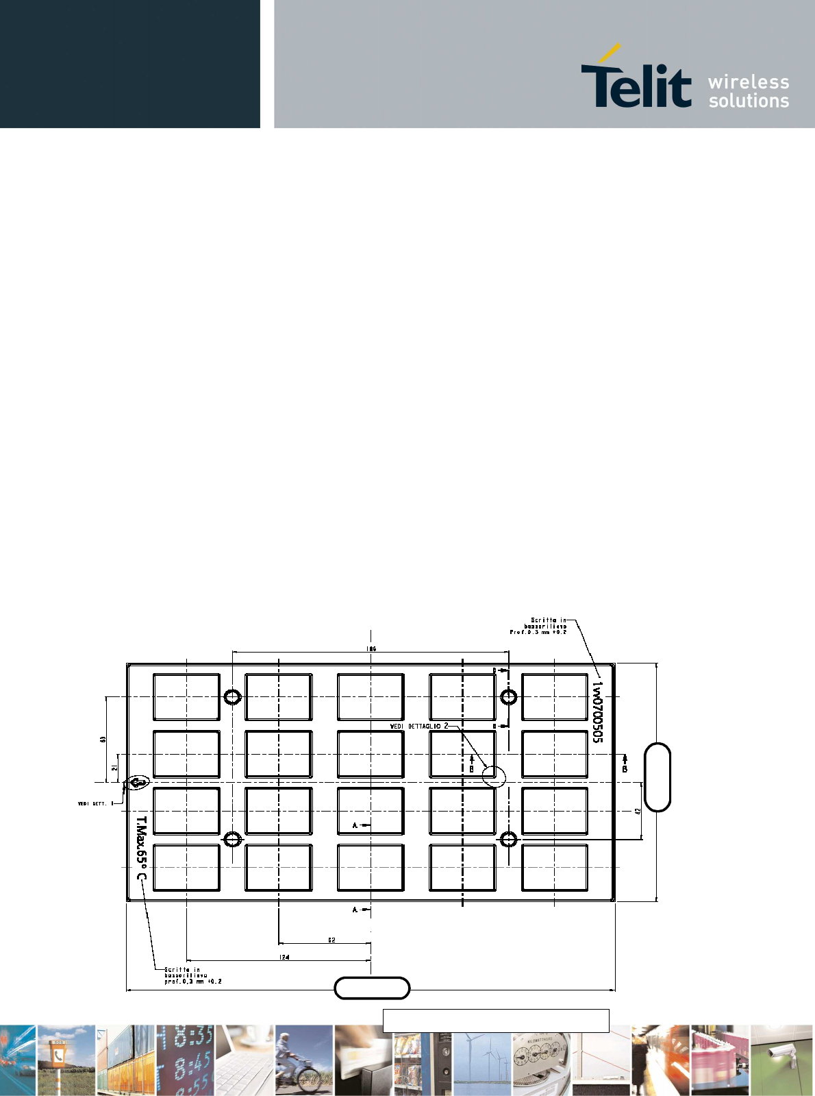
GE863-PRO
3
Product Description
80285ST10036a Rev. 1 DRAFT- 24/04/08
Reproduction forbidden without Telit Communications S.p.A. written authorization - All Rights Reserved page 37 of 53
5 Mounting the GE863-PRO3 on the
Application Board
5.1.1 General
The Telit GE863-PRO
3
module has been designed in order to be compliant with a standard lead-free SMT
process. For detailed information about PCB pad design and conditions to use in SMT process please
consult Hardware User Guide.
5.1.2 Packing system
According to SMT processes for pick & place movement requirements, Telit GE863-PRO
3
modules are
packaged on trays, each tray contains 20 pieces. Tray dimensions are:
320 ± 0,3
170 ± 0,3
All quotes are in mm, general tolerance ± 0.1
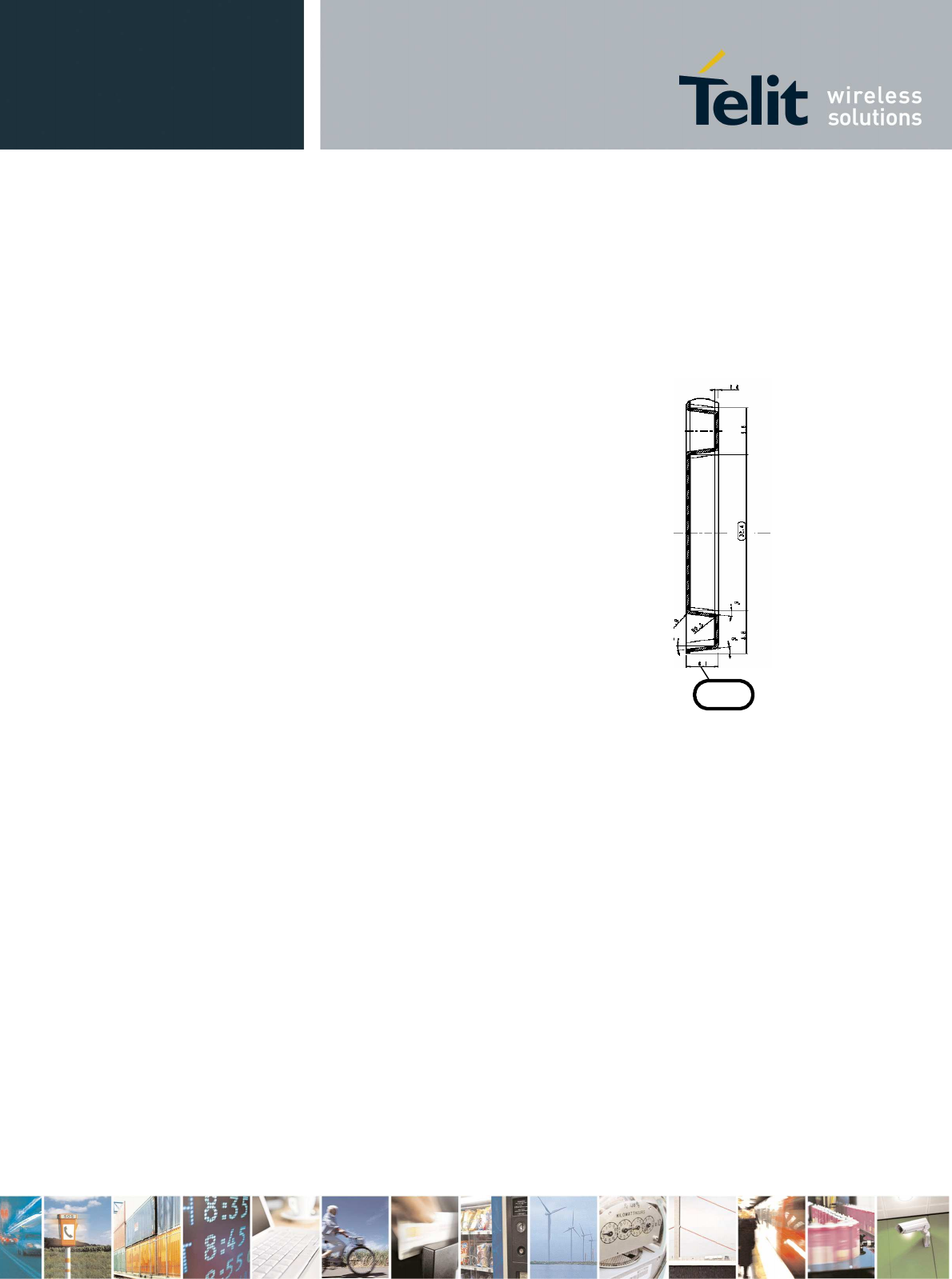
GE863-PRO
3
Product Description
80285ST10036a Rev. 1 DRAFT- 24/04/08
Reproduction forbidden without Telit Communications S.p.A. written authorization - All Rights Reserved page 38 of 53
Note that trays can withstand a maximum temperature of 65° C.
6.1
Section A-A
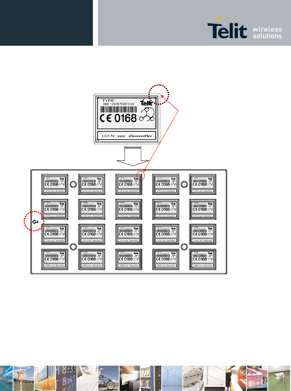
GE863-PRO
3
Product Description
80285ST10036a Rev. 1 DRAFT- 24/04/08
Reproduction forbidden without Telit Communications S.p.A. written authorization - All Rights Reserved page 39 of 53
Modules orientation on tray:
Ref. Not rounded corner
of module’s printed board
indicates pin A1 corner.
The modules in the tray are
oriented as shown in A and
the tray is oriented toward
left as shown in B.
B
A

GE863-PRO
3
Product Description
80285ST10036a Rev. 1 DRAFT- 24/04/08
Reproduction forbidden without Telit Communications S.p.A. written authorization - All Rights Reserved page 40 of 53
6 Evaluation Kit EVK-PRO3
In order to assist you in the development of your Telit GE863-PRO
3
module based application, Telit can
supply an Evaluation Kit EVK-PRO
3
with appropriate power supply, SIM card holder, RS232 serial port
level translator and USB host & device, SD Card holder, SAM Card holder, Ethernet and antenna
connection.
The development of the applications utilizing the Telit GE863-PRO
3
module must present a proper design
of all the interfaces towards and from the module (e.g. power supply, audio paths, level translators),
otherwise a decrease in the performances will be introduced or, in the worst case, a wrong design can
even lead to an operating failure of the module.
In order to assist the hardware designer in his design phase, the EVK board presents a series of
different solutions, which will cover the most common design requirements on the market, and which
can be easily integrated in the OEM design as building blocks or can be taken as starting points to
develop a specific one.
For a detailed description of the Telit GE863-PRO
3
Evaluation Kit refer to the documentation
provided with the Telit GE863-PRO
3
Hardware User Guide and User Manual.

GE863-PRO
3
Product Description
80285ST10036a Rev. 1 DRAFT- 24/04/08
Reproduction forbidden without Telit Communications S.p.A. written authorization - All Rights Reserved page 41 of 53
7 Conformity Assessment Issues
The Telit GE863-PRO
3
modules are assessed to be conform to the R&TTE Directive.
If the module is installed in conformance with Telit installation instructions it will require no further
evaluation under Article 3.2 of the R&TTE Directive and do not require further involvement of an
R&TTE Directive Notified Body for the final product.
In all other cases, or if the manufacturer of the final product is in doubt then the equipment integrating
the radio module must be assessed against Article 3.2 of the R&TTE Directive.
In all the cases, the assessment of the final product must be made against the Essential requirements
of the R&TTE Directive Articles 3.1(a) and (b), safety and EMC respectively, and any relevant Article
3.3 requirements.
The Telit GE863-PRO
3
modules are conforming to the following European Union Directives:
• R&TTE Directive 1999/5/EC (Radio Equipment & Telecommunications Terminal Equipments)
• Low Voltage Directive 73/23/EEC and product safety
• Directive 89/336/EEC for conformity for EMC
In order to satisfy the essential requisite of the R&TTE 99/5/EC directive, the GE863-PRO
3
module is
compliant with the following standards:
• GSM (Radio Spectrum). Standard: EN 301 511 and 3GPP 51.010-1
• EMC (Electromagnetic Compatibility). Standards: EN 301 489-1 and EN 301 489-7
• LVD (Low Voltage Directive) Standards: EN 60 950
Furthermore the Telit GE863-PRO
3
modules are FCC Approved as module to be installed in other
devices. These devices have to be used only for fixed and mobile applications. If the final product after
integration is intended for portable use, a new application and FCC ID is required.
The Telit GE863-PRO
3
modules are conforming to the following US Directives:
• Use of RF Spectrum. Standards: FCC 47 Part 24 (GSM850 - GSM 1900)
• EMC (Electromagnetic Compatibility). Standards: FCC47 Part 15
The GE863-PRO3 module complies with Part 15 of the FCC Rules. Operation is subject to the
following two conditions: (1) this device may not cause harmful interference, and (2) this device must
accept any interference received, including interference that may cause undesired operation.

GE863-PRO
3
Product Description
80285ST10036a Rev. 1 DRAFT- 24/04/08
Reproduction forbidden without Telit Communications S.p.A. written authorization - All Rights Reserved page 42 of 53
The FCC requires the user to be notified that any changes or modifications made to this device that
are not expressly approved by Telit Communications S.p.A. may void the user’s authority to operate
the equipment.
To meet the FCC’s RF exposure rules and regulations:
• The antenna(s) used for this transmitter must be installed to provide a separation distance of at
least 20 cm from all the persons and must not be co-located or operating in conjunction with any
other antenna or transmitter.
• The antenna(s) used for this module must not exceed 3 dBi for mobile and fixed or mobile
operating configurations.
Manufacturers of mobile, fixed or portable devices incorporating this module are advised to clarify any
regulatory questions and to have their complete product tested and approved for FCC compliance.
Interference statement:
The Telit GE863-PRO
3
module complies with Part 15 of the FCC Rules. Operation is subject to the
following two conditions:
• this device may not cause harmful interference, and
• this device must accept any interference received, including interference that may
cause undesired operation.
For questions regarding your product or this FCC declaration, contact:
Telit wireless solutions Inc.
Americas
3131 RDU Center Drive,
USA – 27560 Morrisville, NC 27560, USA
Phone: +1 888 846 9773
Fax: + 1 888 846 9774
e-mail: americas.info@telit.com
To identify this product, refer to the Part, Series, or Model number found on the product.

GE863-PRO
3
Product Description
80285ST10036a Rev. 1 DRAFT- 24/04/08
Reproduction forbidden without Telit Communications S.p.A. written authorization - All Rights Reserved page 43 of 53
7.1 GE863-PRO
3
: Conformity Assessment
GE863-PRO
3
Product Description
80285ST10036a Rev. 1 DRAFT- 24/04/08
Reproduction forbidden without Telit Communications S.p.A. written authorization - All Rights Reserved page 44 of 53

GE863-PRO
3
Product Description
80285ST10036a Rev. 1 DRAFT- 24/04/08
Reproduction forbidden without Telit Communications S.p.A. written authorization - All Rights Reserved page 45 of 53
7.2 GE863-PRO
3
: FCC Equipment Authorization

GE863-PRO
3
Product Description
80285ST10036a Rev. 1 DRAFT- 24/04/08
Reproduction forbidden without Telit Communications S.p.A. written authorization - All Rights Reserved page 46 of 53
7.3 GE863- PRO
3
: IC Equipment Authorization

GE863-PRO
3
Product Description
80285ST10036a Rev. 1 DRAFT- 24/04/08
Reproduction forbidden without Telit Communications S.p.A. written authorization - All Rights Reserved page 47 of 53
7.4 GE863-PRO
3
: RoHS certificate

GE863-PRO
3
Product Description
80285ST10036a Rev. 1 DRAFT- 24/04/08
Reproduction forbidden without Telit Communications S.p.A. written authorization - All Rights Reserved page 48 of 53
8 Safety Recommandations
READ CAREFULLY
Be sure the use of this product is allowed in the country and in the environment required. The use of
this product may be dangerous and has to be avoided in the following areas:
Where it can interfere with other electronic devices in environments such as hospitals, airports,
aircrafts, etc
Where there is risk of explosion such as gasoline stations, oil refineries, etc
It is responsibility of the user to enforce the country regulation and the specific environment regulation.
Do not disassemble the product; any mark of tampering will compromise the warranty validity.
We recommend following the instructions of the hardware user guides for a correct wiring of the
product. The product has to be supplied with a stabilized voltage source and the wiring has to be
conforming to the security and fire prevention regulations.
The product has to be handled with care, avoiding any contact with the pins because electrostatic
discharges may damage the product itself. Same cautions have to be taken for the SIM, checking
carefully the instruction for its use. Do not insert or remove the SIM when the product is in power
saving mode.
The system integrator is responsible of the functioning of the final product; therefore, care has to be
taken to the external components of the module, as well as of any project or installation issue,
because the risk of disturbing the GSM network or external devices or having impact on the security.
Should there be any doubt, please refer to the technical documentation and the regulations in force.
Every module has to be equipped with a proper antenna with specific characteristics. The antenna has
to be installed with care in order to avoid any interference with other electronic devices and has to
guarantee a minimum distance from the body (20 cm). In case of this requirement cannot be satisfied,
the system integrator has to assess the final product against the SAR regulation.
The European Community provides some Directives for the electronic equipments introduced on the
market. All the relevant information’s are available on the European Community website:
http://europa.eu.int/comm/enterprise/rtte/dir99-5.htm
The text of the Directive 99/05 regarding telecommunication equipments is available, while the
applicable Directives (Low Voltage and EMC) are available at:
http://europa.eu.int/comm/enterprise/electr_equipment/index_en.htm

GE863-PRO
3
Product Description
80285ST10036a Rev. 1 DRAFT- 24/04/08
Reproduction forbidden without Telit Communications S.p.A. written authorization - All Rights Reserved page 49 of 53
9 GE863-PRO3 Technical Support
Telit’s technical support to GE863-PRO
3
wireless modem customers consists in:
• Technical documentation: available for download into the Website www.telit.com >Products
>Modules > selected model.
• Engineering support: accessible via E-Mail service with 48 hr replies assured under normal
conditions.
GE863-PRO
3
Product Description
80285ST10036a Rev. 1 DRAFT- 24/04/08
Reproduction forbidden without Telit Communications S.p.A. written authorization - All Rights Reserved page 50 of 53
10 List of acronyms
ACM Accumulated Call Meter
ADC Analog Digital Converter
ASCII American Standard Code for Information Interchange
AT Attention commands
BGA Ball Grid Array (of solder balls on surface mount devices)
CB Cell Broadcast
CBS Cell Broadcasting Service
CCM Call Control Meter
CLIP Calling Line Identification Presentation
CLIR Calling Line Identification Restriction
CMOS Complementary Metal-Oxide Semiconductor
CR Carriage Return
CSD Circuit Switched Data
CTS Clear To Send
DAI Digital Audio Interface
DCD Data Carrier Detected
DCE Data Communications Equipment
DRX Data Receive
DSR Data Set Ready
DTA Data Terminal Adaptor
DTE Data Terminal Equipment
DTMF Dual Tone Multi Frequency
DTR Data Terminal Ready
EMC Electromagnetic Compatibility
ETSI European Telecommunications Equipment Institute
FTA Full Type Approval (ETSI)
FTP File Transfer Protocol
GGA Global Positioning System Fix Data
GLL Geographic Posotion – Latitude/Longitude
GPS Global Positioning System, based on reception of signals from orbiting satellites
GPIO General Purpose Input/Output
GPRS General Radio Packet Service
GSA GPS receiver operating mode, SVs used for navigation, and DOP values.
GSM Global System for Mobile communication
GSV Number of SVs in view, PRN numbers, elevation, azimuth & SNR values.
HF Hands Free
IMEI International Mobile Equipment Identity
IMSI International Mobile Subscriber Identity
IRA International Reference Alphabet
GE863-PRO
3
Product Description
80285ST10036a Rev. 1 DRAFT- 24/04/08
Reproduction forbidden without Telit Communications S.p.A. written authorization - All Rights Reserved page 51 of 53
ITU International Telecommunications Union
IWF Inter-Working Function
JTAG Joint Test Action Group
LCD Liquid Crystal Display
LED Light Emitting Diode
LF Linefeed
ME Mobile Equipment
MMC Multi Media Card
MMI Man Machine Interface
MO Mobile Originated
MS Mobile Station
MT Mobile Terminated
NMEA National Marine Electronics Association
OEM Other Equipment Manufacturer
PB Phone Book
PDU Protocol Data Unit
PH Packet Handler
PIN Personal Identity Number
PLMN Public Land Mobile Network
PPS Precision Positioning Service
PUCT Price per Unit Currency Table
PUK PIN Unblocking Code
PWM Pulse Width Modulation
RACH Random Access Channel
RLP Radio Link Protocol
RMC Recommended Minimum Specific GPS/TRANSIT Data
RMS Root Mean Square
RoHS Reduction of Hazardous Substances
RTS Ready To Send
RI Ring Indicator
SAM Security Authentication Module
SCA Service Center Address
SD Secure Digital
SIM Subscriber Identity Module
SMD Surface Mounted Device
SMS Short Message Service
SMSC Short Message Service Center
SPS Standard Positioning Service
SS Supplementary Service
SPI Serial Peripheral Interface
TIA Telecommunications Industry Association
TTFF Time To First Fix
UART Universal Asynchronous Receiver/Transmitter
UDUB User Determined User Busy
USB Universal Serial Bus

GE863-PRO
3
Product Description
80285ST10036a Rev. 1 DRAFT- 24/04/08
Reproduction forbidden without Telit Communications S.p.A. written authorization - All Rights Reserved page 52 of 53
USSD Unstructured Supplementary Service Data
USART Universal Sinchronous Asynchronous Receiver/Transmitter
VTG Actual track made good and speed over ground
GE863-PRO
3
Product Description
80285ST10036a Rev. 1 DRAFT- 24/04/08
Reproduction forbidden without Telit Communications S.p.A. written authorization - All Rights Reserved page 53 of 53
11 Document Change Log
Revision Date Changes
ISSUE#0 24/08/07 Initial Release