Telit Communications S p A CL865-DUAL CDMA 1x Module User Manual CL865 DUAL Hardware User Guide
Telit Communications S.p.A. CDMA 1x Module CL865 DUAL Hardware User Guide
UserManual.wiki
>
Telit Communications S p A
>
CL865 DUAL User Manual
Users Manual
Navigation menu
Upload a User Manual
Namespaces
Wiki Guide
HTML
PDF
Info
Views
User Manual
Discussion / Help
Navigation


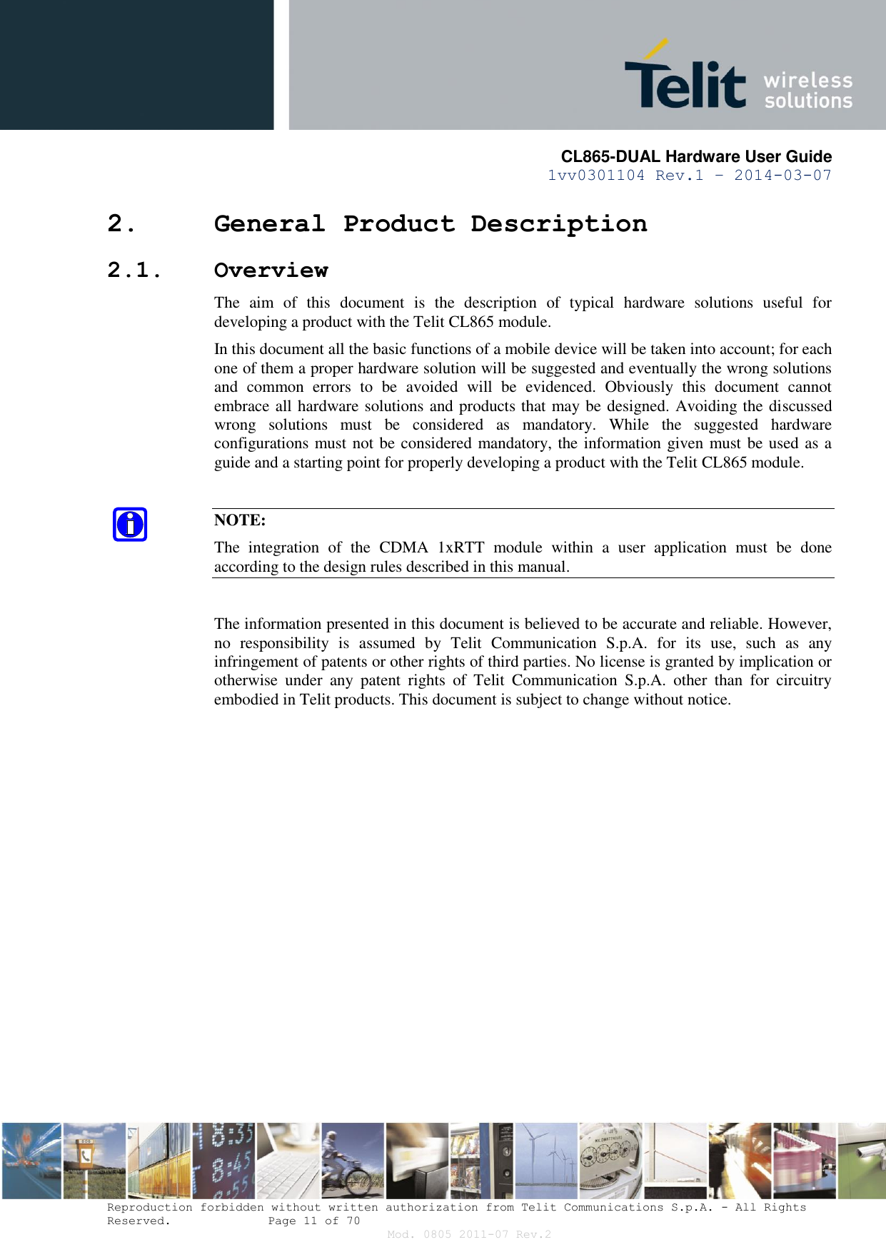

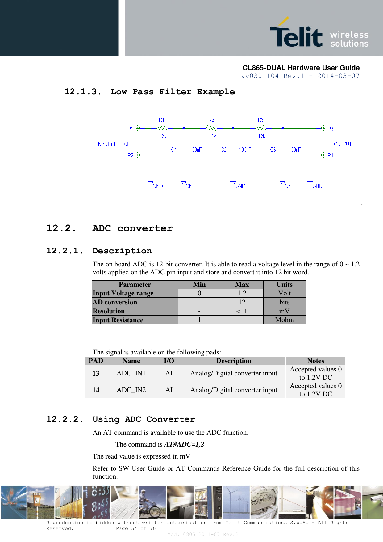
![CL865-DUAL Hardware User Guide 1vv0301104 Rev.1 – 2014-03-07 Reproduction forbidden without written authorization from Telit Communications S.p.A. - All Rights Reserved. Page 53 of 70 Mod. 0805 2011-07 Rev.2 12. DAC and ADC Section 12.1. DAC converter 12.1.1. Description The CL865 module provides a Digital to Analog Converter. The signal (named DAC_OUT) is available on pin 15 of the CL865 module. The on board DAC is in the range from 0 to 1023. However, an external low-pass filter is necessary. Parameter Min Max Units Voltage range (filtered) 0 1.8 Volt Range 0 1023 Steps The precision is 1023 steps, so since the maximum voltage is 1.8V, the integrated voltage could be calculated with the following formula: Integrated output voltage = 1.8 * value / 1023 DAC_OUT line must be integrated (for example with a low band pass filter) in order to obtain an analog voltage. 12.1.2. Enabling DAC An AT command is available to use the DAC function. The command is: AT#DAC[=<enable>[,<value>]] <value> - scale factor of the integrated output voltage (0..1023 ~ 10 bit precision) it must be present if <enable>=1 Refer to SW User Guide or AT Commands Reference Guide for the full description of this function. NOTE: The DAC frequency is selected internally. D/A converter must not be used during POWERSAVING.](https://usermanual.wiki/Telit-Communications-S-p-A/CL865-DUAL/User-Guide-2234575-Page-53.png)
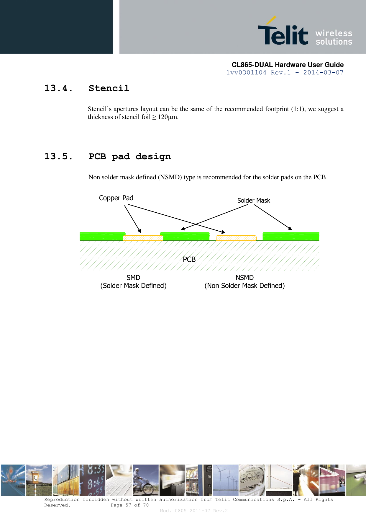
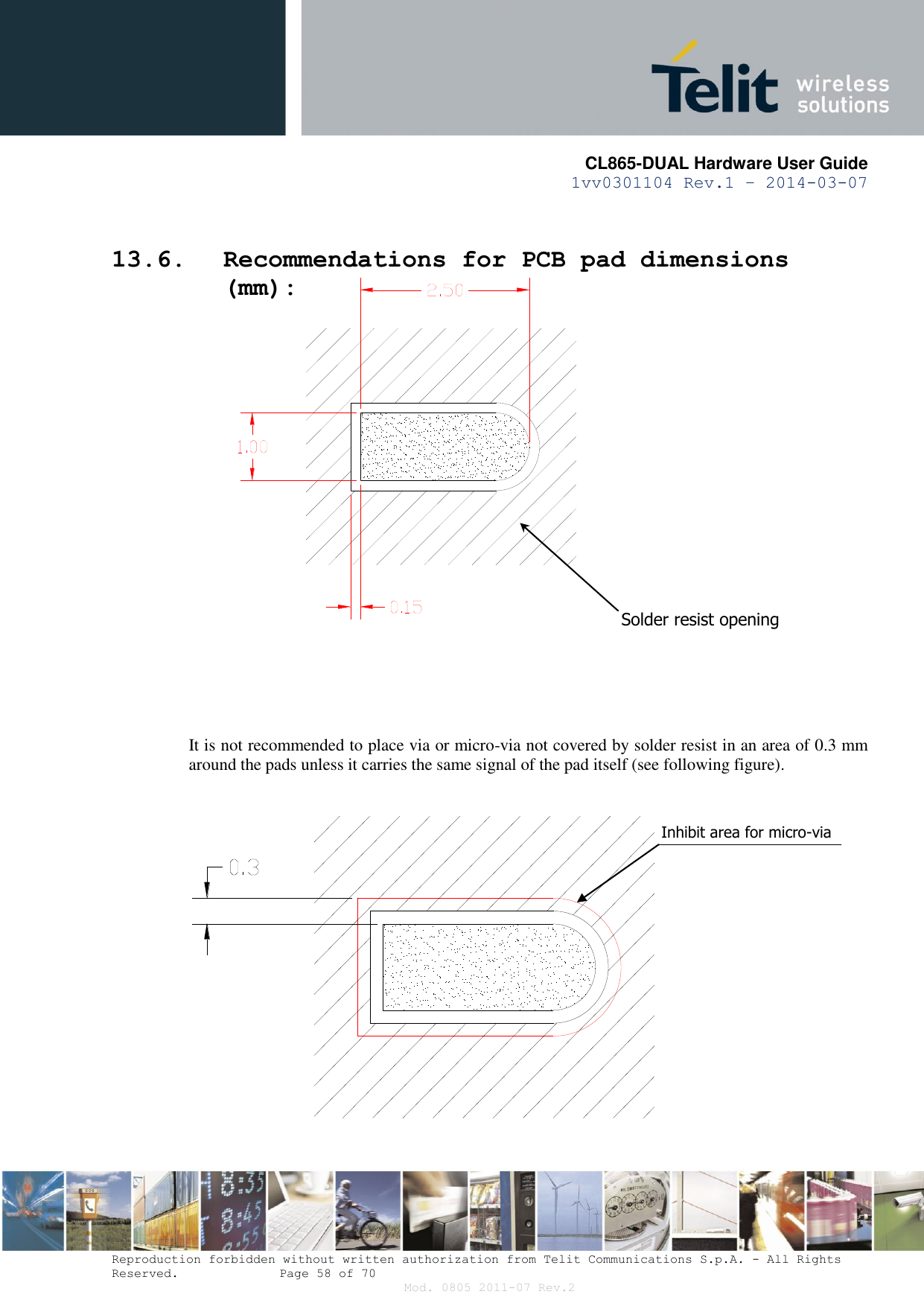
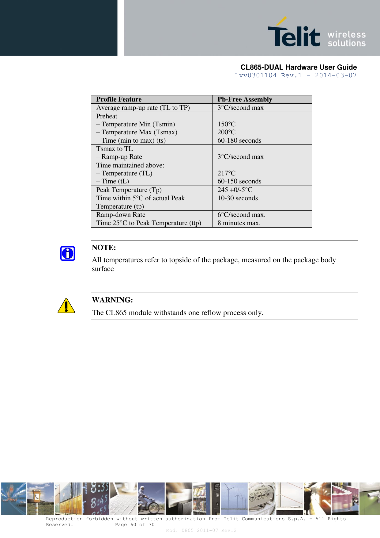
![CL865-DUAL Hardware User Guide 1vv0301104 Rev.1 – 2014-03-07 Reproduction forbidden without written authorization from Telit Communications S.p.A. - All Rights Reserved. Page 59 of 70 Mod. 0805 2011-07 Rev.2 Holes in pad are allowed only for blind holes and not for through holes. Recommendations for PCB pad surfaces: Finish Layer thickness [µm] Properties Electro-less Ni / Immersion Au 3 –7 / 0.05 – 0.15 good solder ability protection, high shear force values The PCB must be able to resist the higher temperatures which are occurring at the lead-free process. This issue should be discussed with the PCB-supplier. Generally, the wettability of tin-lead solder paste on the described surface plating is better compared to lead-free solder paste. It is not necessary to panel the application PCB, however in that case it is suggested to use milled contours and predrilled board breakouts; scoring or v-cut solutions are not recommended. 13.7. Solder paste Lead free Solder paste Sn/Ag/Cu We recommend using only “no clean” solder paste in order to avoid the cleaning of the modules after assembly. 13.8. CL865 Solder reflow Recommended solder reflow profile TL Tsmin Tsmax ts tL tp ttp](https://usermanual.wiki/Telit-Communications-S-p-A/CL865-DUAL/User-Guide-2234575-Page-59.png)