Telit Communications S p A DE910-DUAL DUAL BAND CDMA/GPS module User Manual
Telit Communications S.p.A. DUAL BAND CDMA/GPS module
Contents
- 1. user manual
- 2. antenna information
- 3. User Manual
user manual

Preliminary
DE910-DUAL
Hardware User Guide
1vv0300951 Rev.1 – 2011-12-09

HW User Guide Template
1vv0300951 Rev.1 – 2011-12-
Reproduction forbidden without written authorization from Telit Communications S.p.A. - All Rights
Reserved. Page 2 of 60
APPLICABILITY TABLE
PRODUCT
DE910-DUAL

HW User Guide Template
1vv0300951 Rev.1 – 2011-12-
Reproduction forbidden without written authorization from Telit Communications S.p.A. - All Rights
Reserved. Page 3 of 60
SPECIFICATIONS SUBJECT TO CHANGE WITHOUT NOTICE
Notice
While reasonable efforts have been made to assure the accuracy of this document, Telit
assumes no liability resulting from any inaccuracies or omissions in this document, or from
use of the information obtained herein. The information in this document has been carefully
checked and is believed to be entirely reliable. However, no responsibility is assumed for
inaccuracies or omissions. Telit reserves the right to make changes to any products described
herein and reserves the right to revise this document and to make changes from time to time
in content hereof with no obligation to notify any person of revisions or changes. Telit does
not assume any liability arising out of the application or use of any product, software, or
circuit described herein; neither does it convey license under its patent rights or the rights of
others.
It is possible that this publication may contain references to, or information about Telit
products (machines and programs), programming, or services that are not announced in your
country. Such references or information must not be construed to mean that Telit intends to
announce such Telit products, programming, or services in your country.
Copyrights
This instruction manual and the Telit products described in this instruction manual may be,
include or describe copyrighted Telit material, such as computer programs stored in
semiconductor memories or other media. Laws in the Italy and other countries preserve for
Telit and its licensors certain exclusive rights for copyrighted material, including the
exclusive right to copy, reproduce in any form, distribute and make derivative works of the
copyrighted material. Accordingly, any copyrighted material of Telit and its licensors
contained herein or in the Telit products described in this instruction manual may not be
copied, reproduced, distributed, merged or modified in any manner without the express
written permission of Telit. Furthermore, the purchase of Telit products shall not be deemed
to grant either directly or by implication, estoppel, or otherwise, any license under the
copyrights, patents or patent applications of Telit, as arises by operation of law in the sale of a
product.
Computer Software Copyrights
The Telit and 3rd Party supplied Software (SW) products described in this instruction manual
may include copyrighted Telit and other 3rd Party supplied computer programs stored in
semiconductor memories or other media. Laws in the Italy and other countries preserve for
Telit and other 3rd Party supplied SW certain exclusive rights for copyrighted computer
programs, including the exclusive right to copy or reproduce in any form the copyrighted
computer program. Accordingly, any copyrighted Telit or other 3rd Party supplied SW
computer programs contained in the Telit products described in this instruction manual may
not be copied (reverse engineered) or reproduced in any manner without the express written
permission of Telit or the 3rd Party SW supplier. Furthermore, the purchase of Telit products
shall not be deemed to grant either directly or by implication, estoppel, or otherwise, any
license under the copyrights, patents or patent applications of Telit or other 3rd Party supplied
SW, except for the normal non-exclusive, royalty free license to use that arises by operation
of law in the sale of a product.

HW User Guide Template
1vv0300951 Rev.1 – 2011-12-
Reproduction forbidden without written authorization from Telit Communications S.p.A. - All Rights
Reserved. Page 4 of 60
Usage and Disclosure Restrictions
License Agreements
The software described in this document is the property of Telit and its licensors. It is
furnished by express license agreement only and may be used only in accordance with the
terms of such an agreement.
Copyrighted Materials
Software and documentation are copyrighted materials. Making unauthorized copies is
prohibited by law. No part of the software or documentation may be reproduced, transmitted,
transcribed, stored in a retrieval system, or translated into any language or computer language,
in any form or by any means, without prior written permission of Telit
High Risk Materials
Components, units, or third-party products used in the product described herein are NOT
fault-tolerant and are NOT designed, manufactured, or intended for use as on-line control
equipment in the following hazardous environments requiring fail-safe controls: the operation
of Nuclear Facilities, Aircraft Navigation or Aircraft Communication Systems, Air Traffic
Control, Life Support, or Weapons Systems (High Risk Activities"). Telit and its supplier(s)
specifically disclaim any expressed or implied warranty of fitness for such High Risk
Activities.
Trademarks
TELIT and the Stylized T Logo are registered in Trademark Office. All other product or
service names are the property of their respective owners.
Copyright © Telit Communications S.p.A. 2011.

HW User Guide Template
1vv0300951 Rev.1 – 2011-12-
Reproduction forbidden without written authorization from Telit Communications S.p.A. - All Rights
Reserved. Page 5 of 60
Contents
1. Introduction ................................................. 8
1.1. Scope ..................................................... 8
1.2. Audience .................................................. 8
1.3. Contact Information, Support .............................. 8
1.4. Document Organization ..................................... 9
1.5. Text Conventions .......................................... 9
1.6. Related Documents ........................................ 10
2. General Product Description ................................. 11
2.1. Overview ................................................. 11
2.2. 2D Mechanical Dimensions ................................. 11
2.3. Weight ................................................... 11
2.4. Environmental Requirements ............................... 12
2.4.1. Temperature Range .......................................... 12
2.5. RoHS Compliance .......................................... 12
2.6. Operating Frequency ...................................... 12
3. DE910-DUAL Module Connections ............................... 13
3.1. Pin-Out .................................................. 13
3.1.1. LGA Pads Layout ............................................ 18
4. Hardware Commands ........................................... 19
4.1. Turning on the DE901-DUAL module ......................... 19
4.1.1. Initialization and Activation State ........................ 19
4.2. Turning off the DE901-DUAL module ........................ 21
4.2.1. Shutdown by Software Command ............................... 21
4.2.2. Hardware Shutdown .......................................... 22
4.2.3. Hardware Unconditional Reboot .............................. 23
4.3. Summary of Turning ON and OFF the Module ................. 24
5. Power Supply ................................................ 25
5.1. Power Supply Requirements ................................ 25
5.2. General Design Rules ..................................... 25
5.2.1. Electrical Design Guidelines ............................... 26
5.2.2. Thermal Design Guidelines .................................. 29

HW User Guide Template
1vv0300951 Rev.1 – 2011-12-
Reproduction forbidden without written authorization from Telit Communications S.p.A. - All Rights
Reserved. Page 6 of 60
5.2.3. Power Supply PCB layout Guidelines ......................... 30
6. Antenna (Antenne) ........................................... 31
6.1. CDMA Antenna Requirements (Specifications de l’antenne CDMA)
31
6.2. CDMA antenna – PCB line Guidelines (Antenne CDMA –
Directives pour le PCB) ........................................ 33
6.3. CDMA Antenna installation Guidelines (Directives d’installation de
l’antenne CDMA) .................................................. 34
6.4. Antenna Diversity Requirements (Conditions de diversité
d’antenne) ..................................................... 35
6.5. GPS Antenna Requirements ................................. 36
6.5.1. Combined GPS Antenna ....................................... 36
6.5.2. Linear and Patch GPS Antenna ............................... 36
6.5.3. LNA and Front End Design Considerations .................... 36
6.5.4. GPS Antenna - PCB Line Guidelines .......................... 37
6.5.5. GPS Antenna – Installation Guidelines ...................... 37
7. USB Port .................................................... 38
8. SPI Port (TBD) .............................................. 39
8.1. SPI Connections .......................................... 39
9. Serial Port ................................................. 40
9.1. Modem Serial Port 1 ...................................... 41
9.2. Modem Serial Port 2 ...................................... 42
9.3. RS232 Level Translation .................................. 42
10. Audio Section Overview ...................................... 44
10.1. Electrical Characteristics ............................. 44
10.1.1. CODEC Example ............................................ 44
11. General Purpose I/O ......................................... 45
11.1. Logic Level Specification .............................. 46
11.2. Using a GPIO Pad as Input .............................. 46
11.3. Using a GPIO Pad as Output ............................. 47
11.4. Using the Temperature Monitor Function ................. 47
11.4.1. Short Description ........................................ 47
11.5. Indication of Network Service Availability ............. 48

HW User Guide Template
1vv0300951 Rev.1 – 2011-12-
Reproduction forbidden without written authorization from Telit Communications S.p.A. - All Rights
Reserved. Page 7 of 60
11.6. RTC Bypass output ...................................... 48
11.7. VAUX/PWRMON Power Output ............................... 49
12. Mounting the Module on your Board ........................... 50
12.1. General ................................................ 50
12.2. Module Finishing & Dimensions .......................... 50
12.3. DE910-DUAL Mechanical Dimensions ....................... 51
12.4. Recommended foot print for the application ............. 52
12.5. Stencil ................................................ 53
12.6. PCB Pad Design ......................................... 53
12.7. Recommendations for PCB Pad Dimensions mm) ............. 53
12.8. Recommendations for PCB Pad Surfaces ................... 54
12.9. Solder Paste ........................................... 54
12.10. Solder Reflow .......................................... 54
12.11. Packing System ......................................... 55
12.11.1. Tray Drawing ............................................. 55
12.12. Moisture Sensibility ................................... 55
13. Conformity Assessment Issues (Problèmes d'évaluation de
conformité)...................................................... 56
14. Safety Recommendations ...................................... 59
15. Document History ............................................ 60
HW User Guide Template
1vv0300951 Rev.1 – 2011-12-
Reproduction forbidden without written authorization from Telit Communications S.p.A. - All Rights
Reserved. Page 8 of 60
1. Introduction
1.1. Scope
The aim of this document is the description of typical hardware solutions useful for
developing a product with the Telit DE910-DUAL module.
1.2. Audience
This document is intended for Telit customers, who are integrators, about to implement their
applications using our DE910-DUAL modules.
1.3. Contact Information, Support
For general contact, technical support, to report documentation errors and to order manuals,
contact Telit Technical Support Center (TTSC) at:
TS-EMEA@telit.com
TS-NORTHAMERICA@telit.com
TS-LATINAMERICA@telit.com
TS-APAC@telit.com
Alternatively, use:
http://www.telit.com/en/products/technical-support-center/contact.php
For detailed information about where you can buy the Telit modules or for recommendations
on accessories and components visit:
http://www.telit.com
To register for product news and announcements or for product questions contact Telit
Technical Support Center (TTSC).
Our aim is to make this guide as helpful as possible. Please keep us informed of your
comments and suggestions for improvements.
Telit appreciates feedback from the users of our information.
HW User Guide Template
1vv0300951 Rev.1 – 2011-12-
Reproduction forbidden without written authorization from Telit Communications S.p.A. - All Rights
Reserved. Page 9 of 60
1.4. Document Organization
This document contains the following chapters:
Chapter 1: “Introduction” provides a scope for this document, target audience, contact and
support information, and text conventions.
Chapter 2: “General Product Description” gives an overview of the features of the product.
Chapter 3: “DE910-DUAL Module Connections” deals with the pin out configuration and
layout.
Chapter 4: “Hardware Commands” How to operate the module via hardware.
Chapter 5: “Power supply” Power supply requirements and general design rules.
Chapter 6: “Antenna” The antenna connection and board layout design are the most important
parts in the full product design.
Chapter 7: “USB Port” The USB port on the Telit DE910-DUAL is the core of the interface
between the module and OEM hardware.
Chapter 8: “Serial ports” Refers to the serial ports of the Telit DE910-DUAL.
Chapter 9: “Audio Section overview” Refers to the audio blocks of the Base Band Chip of the
DE910-DUAL Telit Module.
Chapter 10: “General Purpose I/O” How the general purpose I/O pads can be configured.
Chapter 11: “Mounting the DE910-DUAL on the application board” Mechanical dimensions
and recommendations on how to mount the module on the user’s board.
Chapter 12: “Conformity Assessment Issues” provides some fundamental hints about the
conformity assessment that the final application might need.
Chapter 13: “Safety Recommendation” provides some safety recommendations that must be
followed by the customer in the design of the application that makes use of the Telit DE910-
DUAL.
1.5. Text Conventions
Danger – This information MUST be followed or catastrophic equipment failure or bodily
injury may occur.
Caution or Warning – Alerts the user to important points about integrating the module, if
these points are not followed, the module and end user equipment may fail or malfunction.
Tip or Information – Provides advice and suggestions that may be useful when
integrating the module.
All dates are in ISO 8601 format, i.e. YYYY-MM-DD.

HW User Guide Template
1vv0300951 Rev.1 – 2011-12-
Reproduction forbidden without written authorization from Telit Communications S.p.A. - All Rights
Reserved. Page 10 of 60
1.6. Related Documents
• Digital voice Interface Application Note, TBD
• DE910-DUAL Product description, 80392ST10096A
• R-UIM Holder Design Guide, TBD
• Telit EVK2 User Guide, 1vv0300704
HW User Guide Template
1vv0300951 Rev.1 – 2011-12-
Reproduction forbidden without written authorization from Telit Communications S.p.A. - All Rights
Reserved. Page 11 of 60
2. General Product Description
2.1. Overview
The aim of this document is the description of typical hardware solutions useful for
developing a product with the Telit DE910-DUAL module.
In this document all the basic functions of a mobile phone will be taken into account; for each
one of them a proper hardware solution will be suggested and eventually the wrong solutions
and common errors to be avoided will be evidenced. Obviously this document cannot
embrace the all hardware solutions and products that may be designed. The solutions to be
avoided must be considered as mandatory. While the suggested hardware configurations must
not be considered mandatory, the information given must be used as a guide and a starting
point for properly developing your product with the Telit DE910-DUAL module.
NOTE:
The integration of the CDMA 1x / 1xEV-DO module within a user application must be done
according to the design rules described in this manual.
The information presented in this document is believed to be accurate and reliable. However,
no responsibility is assumed by Telit Communication S.p.A. for its use, such as any
infringement of patents or other rights of third parties which may result from its use. No
license is granted by implication or otherwise under any patent rights of Telit Communication
S.p.A. other than for circuitry embodied in Telit products. This document is subject to change
without notice.
2.2. 2D Mechanical Dimensions
• Length: 28.2 mm
• Width: 28.2mm
• Thickness: 2.5mm
2.3. Weight
The module weight of DE910-DUAL is about 4.7 gram.
HW User Guide Template
1vv0300951 Rev.1 – 2011-12-
Reproduction forbidden without written authorization from Telit Communications S.p.A. - All Rights
Reserved. Page 12 of 60
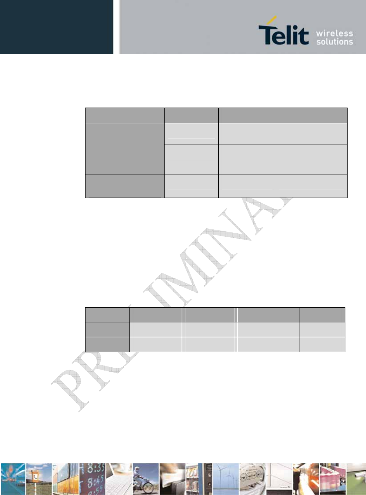
2.4. Environmental Requirements
2.4.1. Temperature Range
Note
Operating Temperature
Range
–30°C ~ +60°C The module is fully functional (*) in all the
temperature range, and it fully meets the 3GPP2
specifications.
–30°C ~ +85°C The module is fully functional (*) in all the
temperature range.
Temperatures outside the range -30 ~ 60℃ might
deviate from 3GPP2 specification.
Storage and non-operating
Temperature Range
–40°C ~ +85°C
(*)Functional: the module is able to make and receive voice calls, data calls, and SMS.
2.5. RoHS Compliance
As a part of Telit’s corporate policy of environmental protection, the DE910-DUAL complies
with the RoHS (Restriction of Hazardous Substances) directive of the European Union (EU
directive 2002/95/EG).
2.6. Operating Frequency
The operating frequencies in US cellular (BC0) and US PCS (BC1) modes comply with the
3GPP2 specifications.
Mode Freq. TX (MHz) Freq. RX (MHz) Channels TX - RX offset
CDMA BC0 824 ~ 849 869 ~ 894 1 ~ 799, 991 ~ 1023 45 MHz
CDMA BC1 1850 ~ 1910 1930 ~ 1990 0 ~ 1199 80 MHz
HW User Guide Template
1vv0300951 Rev.1 – 2011-12-
Reproduction forbidden without written authorization from Telit Communications S.p.A. - All Rights
Reserved. Page 13 of 60
3. DE910-DUAL Module Connections
3.1. Pin-Out
PAD Signal I/O Function Type COMMENT
USB HS 2.0 Communication Port
B15 USB_D+ I/O USB differential Data(+)
C15 USB_D- I/O USB differential Data(+)
A13 VBUS AI Power sense for the internal USB transceiver
Asynchronous UART – Prog. / data +HW Flow Control
N15 C103/TXD I Serial data input (TXD) from DTE 1.8V
M15 C104/RXD O Serial data output to DTE 1.8V
M14 C108/DTR I Input for Data terminal ready signal (DTR) from DTE 1.8V
L14 C105/RTS I Input for Request to send signal (RTS) from DTE 1.8V
P15 C106/CTS O Output for Clear to send signal (CTS) to DTE 1.8V
N14 C109/DCD O Output for Data carrier detect signal (DCD) to DTE 1.8V
P14 C107/DSR O Output for Data set ready signal (DSR) to DTE 1.8V
R14 C125/RING O Output for Ring indicator signal (RI) to DTE 1.8V
Asynchronous Auxiliary UART
D15 TX_AUX O Auxillary UART (TX Data to DTE) 1.8V
E15 RX_AUX I Auxillary UART (RX Data from DTE) 1.8V
SIM Card Interface
A6 SIMCLK O External SIM signal – Clock 1.8/2.85V
A7 SIMRST O External SIM signal – Reset 1.8/2.85V
A5 SIMIO I/O External SIM signal - Data I/O 1.8/2.85V
A4 SIMIN I External SIM signal - Presence (active low) 1.8V
A3 SIMVCC - External SIM signal – Power supply for the SIM 1.8/2.85V
Digital Voice interface (DVI)
B9 DVI_WA0 I/O Digital Voice interface (WA0) 1.8V
B6 DVI_RX I/O Digital Voice interface (RX) 1.8V
B7 DVI_TX I/O Digital Voice interface (TX) 1.8V
B8 DVI_CLK I/O Digital Voice interface (CLK) 1.8V
SPI
D15 SPI_MOSI I/O SPI MOSI 1.8V
E15 SPI_MISO I/O SPI MISO 1.8V
F15 SPI_CLK I/O SPI Clock 1.8V
H14 SPI_CS_N I/O SPI Chip Select 1.8V
HW User Guide Template
1vv0300951 Rev.1 – 2011-12-
Reproduction forbidden without written authorization from Telit Communications S.p.A. - All Rights
Reserved. Page 14 of 60
PAD Signal I/O Function Type COMMENT
Digital IO
C8 GPIO_01 I/O GPIO_01 1.8V
C9 GPIO_02 I/O GPIO_02 1.8V
C10 GPIO_03 I/O GPIO_03 1.8V
C11 GPIO_04 I/O GPIO_04 1.8V
B14 GPIO_05 I/O GPIO_05 1.8V
C12 GPIO_06 I/O GPIO_06 1.8V
C13 GPIO_07 I/O GPIO_07 1.8V
K15 GPIO_08 I/O GPIO_08 1.8V
L15 GPIO_09 I/O GPIO_09 1.8V
G15 GPIO_10 I/O GPIO_10 1.8V
RF Section
K1 Antenna I/O CDMA Antenna (50Ohm) RF
F1 ANT_DIV I CDMA Antenna Diversity Input (50Ohm) RF
GPS Section
R9 ANT_GPS I GPS Antenna (50Ohm) RF
R7 GPS_LNA_EN O Output enable for External LNA supply 1.8V
Miscellaneous Function
R13 RESET* I Reset Input 1.8V Active Low
R12 ON_OFF* I Input Command for Power ON 1.8V Active Low
C14 VRTC AI VRTC Backup Capacitor Power
To be used to
b
ack up the RTC
section
R11 VAUX/PWRMON O Supply Output for External Accessories / Power ON
Monitor 1.8V
Power Supply
M1 VBATT - Main Power Supply (Baseband) Power
M2 VBATT - Main Power Supply (Baseband) Power
N1 VBATT_PA - Main Power Supply (PAM) Power
N2 VBATT_PA - Main Power Supply (PAM) Power
P1 VBATT_PA - Main Power Supply (PAM) Power
P2 VBATT_PA - Main Power Supply (PAM) Power
E1 GND - Ground
G1 GND - Ground
H1 GND - Ground
J1 GND - Ground
L1 GND - Ground
A2 GND - Ground
E2 GND - Ground
F2 GND - Ground
G2 GND - Ground
HW User Guide Template
1vv0300951 Rev.1 – 2011-12-
Reproduction forbidden without written authorization from Telit Communications S.p.A. - All Rights
Reserved. Page 15 of 60
PAD Signal I/O Function Type COMMENT
H2 GND - Ground
J2 GND - Ground
K2 GND - Ground
L2 GND - Ground
R2 GND - Ground
M3 GND - Ground
N3 GND - Ground
P3 GND - Ground
R3 GND - Ground
D4 GND - Ground
M4 GND - Ground
N4 GND - Ground
P4 GND Ground
R4 GND Ground
N5 GND - Ground
P5 GND - Ground
R5 GND - Ground
N6 GND - Ground
P6 GND - Ground
R6 GND - Ground
P8 GND - Ground
R8 GND Ground
P9 GND - Ground
P10 GND - Ground
R10 GND - Ground
M12 GND - Ground
B13 GND - Ground
P13 GND - Ground
E14 GND - Ground
Reserved
B1 Reserved - Reserved
C1 Reserved - Reserved
D1 Reserved - Reserved
B2 Reserved - Reserved
C2 Reserved - Reserved
D2 Reserved - Reserved
B3 Reserved - Reserved
C3 Reserved - Reserved
D3 Reserved - Reserved
E3 Reserved - Reserved
F3 Reserved - Reserved
HW User Guide Template
1vv0300951 Rev.1 – 2011-12-
Reproduction forbidden without written authorization from Telit Communications S.p.A. - All Rights
Reserved. Page 16 of 60
PAD Signal I/O Function Type COMMENT
G3 Reserved - Reserved
H3 Reserved - Reserved
J3 Reserved - Reserved
K3 Reserved - Reserved
L3 Reserved - Reserved
B4 Reserved - Reserved
C4 Reserved - Reserved
B5 Reserved - Reserved
C5 Reserved - Reserved
C6 Reserved - Reserved
C7 Reserved - Reserved
N7 Reserved - Reserved
P7 Reserved - Reserved
A8 Reserved - Reserved
N8 Reserved - Reserved
A9 Reserved - Reserved
N9 Reserved - Reserved
A10 Reserved - Reserved
B10 Reserved - Reserved
N10 Reserved - Reserved
A11 Reserved - Reserved
B11 Reserved - Reserved
N11 Reserved - Reserved
P11 Reserved - Reserved
A12 Reserved - Reserved
B12 Reserved - Reserved
D12 Reserved - Reserved
N12 Reserved - Reserved
P12 Reserved - Reserved
D13 Reserved - Reserved
E13 Reserved - Reserved
F13 Reserved - Reserved
G13 Reserved - Reserved
H13 Reserved - Reserved
J13 Reserved - Reserved
K13 Reserved - Reserved
L13 Reserved - Reserved
M13 Reserved - Reserved
N13 Reserved - Reserved
A14 Reserved - Reserved
D14 Reserved - Reserved
HW User Guide Template
1vv0300951 Rev.1 – 2011-12-
Reproduction forbidden without written authorization from Telit Communications S.p.A. - All Rights
Reserved. Page 17 of 60
PAD Signal I/O Function Type COMMENT
F14 Reserved - Reserved
G14 Reserved - Reserved
J14 Reserved - Reserved
K14 Reserved - Reserved
H15 Reserved - Reserved
J15 Reserved - Reserved
WARNIG:
Reserved pins must not be connected.
NOTE:
Almost all pins not in use must be left disconnected. The only exceptions are the following
pins:
PAD Signal
M1,M2,N1,N2,P1,P2 VBATT & VBATT_PA
E1,G1,H1,J1,L1,A2,E2,F2,G2,H2,J2,K2,L2,R2,M3,
N3,P3,R3,D4,M4,N4,P4,R4,N5,P5,R5,N6,P6,R6,P8,
R8,P9,P10,R10,M12,B13,P13,E14
GND
R12 ON/OFF*
R13 RESET*
B15 USB_D+
C15 USB_D-
A13 VBUS
N15 C103/TXD
M15 C104/RXD
L14 C105/RTS
P15 C106/CTS
D15 TXD_AUX
E15 RXD_AUX
RTS must be connected to the GND (on the module side) if flow control is not used.
The above pins are also necessary to debug the application incorporating the module.
HW User Guide Template
1vv0300951 Rev.1 – 2011-12-
Reproduction forbidden without written authorization from Telit Communications S.p.A. - All Rights
Reserved. Page 18 of 60
3.1.1. LGA Pads Layout
ABCDEFGHJKLMNPR
1B1
RFU
C1
RFU
D1
RFU
E1
GND
F1
ANT_DIV
G1
GND
H1
GND
J1
GND
K1
ANT_MAIN
L1
GND
M1
VBATT
N1
VBATT_PA
P1
VBATT_PA 1
2A2
GND
B2
RFU
C2
RFU
D2
RFU
E2
GND
F2
GND
G2
GND
H2
GND
J2
GND
K2
GND
L2
GND
M2
VBATT
N2
VBATT_PA
P2
VBATT_PA
R2
GND 2
3A3
SIMVCC
B3
RFU
C3
RFU
D3
RFU
E3
RFU
F3
RFU
G3
RFU
H3
RFU
J3
RFU
K3
RFU
L3
RFU
M3
GND
N3
GND
P3
GND
R3
GND 3
4A4
SIMIN
B4
RFU
C4
RFU
D4
GND M4
GND
N4
GND
P4
GND
R4
GND 4
5A5
SIMIO
B5
RFU
C5
RFU
N5
GND
P5
GND
R5
GND 5
6A6
SIMCLK
B6
DVI_RX
C6
RFU
N6
GND
P6
GND
R6
GND 6
7A7
SIMRST
B7
DVI_TX
C7
RFU
N7
RFU
P7
RFU
R7
GPS_LNA_EN
7
8A8
RFU
B8
DVI_CLK
C8
GPIO_01
N8
RFU
P8
GND
R8
GND 8
9A9
RFU
B9
DVI_WA0
C9
GPIO_02
N9
RFU
P9
GND
R9
ANT_GPS 9
10 A10
RFU
B10
RFU
C10
GPIO_03
N10
RFU
P10
GND
R10
GND 10
11 A11
RFU
B11
RFU
C11
GPIO_04
N11
RFU
P11
RFU R11
VAUX/PWRMON
11
12 A12
RFU
B12
RFU
C12
GPIO_06
D12
RFU
M12
GND
N12
RFU
P12
RFU
R12
ON_OFF/ 12
13 A13
USB_VBUS
B13
GND
C13
GPIO_07
D13
RFU
E13
RFU
F13
RFU
G13
RFU
H13
RFU
J13
RFU
K13
RFU
L13
RFU
M13
RFU
N13
RFU
P13
GND
R13
RESET/ 13
14 A14
RFU
B14
GPIO_05
C14
VRTC
D14
RFU
E14
GND
F14
RFU
G14
RFU
H14
SPI_CS_N
J14
RFU
K14
RFU
L14
C105/RTS
M14
C108/DTR
N14
C109/DCD
P14
C107/DSR R14
C125/RING
14
15 B15
USB_D+
C15
USB_D-
D15
TX_AUX
E15
RX_AUX
F15
SPI_CLK
G15
GPIO_10
H15
RFU
J15
RFU
K15
GPIO_08
L15
GPIO_09
M15
C104/RXD
N15
C103/TXD
P15
C106/CTS 15
ABCDEFGHJKLMNPR
NOTE:
The pin defined as RES has to be considered RESERVED and not connected on any pin in
the application. The related area on the application has to be kept empty.
HW User Guide Template
1vv0300951 Rev.1 – 2011-12-
Reproduction forbidden without written authorization from Telit Communications S.p.A. - All Rights
Reserved. Page 19 of 60
4. Hardware Commands
4.1. Turning on the DE901-DUAL module
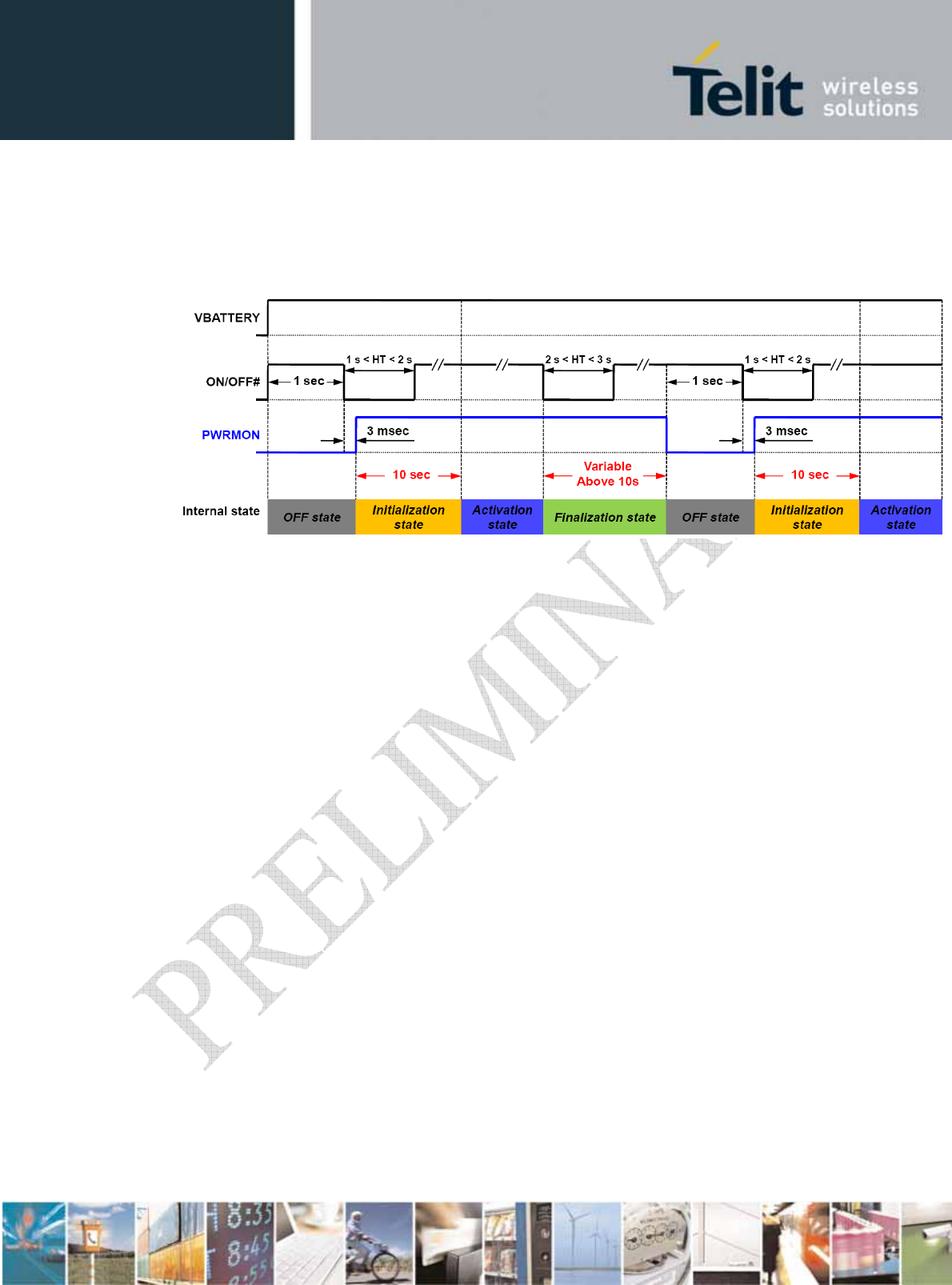
To turn on the DE910-DUAL, the pad ON# must be tied low for at least 1 second and then
released.
The maximum current that can be drained from the ON# pad is 0.1 mA.
A simple circuit to power on the module is illustrated below:
4.1.1. Initialization and Activation State
Upon turning on DE910-DUAL module, the DE910-DUAL module is not active yet because
the boot sequence of DE910-DUAL is still executing internally. It takes about 10 seconds to
complete the initialization of the module internally.
For this reason, it would be useless to try to access DE910-DUAL during the Initialization
state as below. The DE910-DUAL module needs at least 10 seconds after the PWRMON goes
High to become operational by reaching the activation state.
HW User Guide Template
1vv0300951 Rev.1 – 2011-12-
Reproduction forbidden without written authorization from Telit Communications S.p.A. - All Rights
Reserved. Page 20 of 60
During the Initialization state, any kind of AT-command is not available. DTE must wait for
the Activation state to communicate with DE910-DUAL.
To check if the DE910-DUAL has powered on, the hardware line PWRMON must be
monitored. When PWRMON goes high, the module has powered on.
NOTE:
Do not use any pull up resistor on the ON# line. It is pulled up internally. Using a pull up
resistor may bring latch up problems on the DE910-DUAL power regulator and improper
power on/off of the module. The line ON# must be connected only in open collector
configuration.
NOTE:
In this document all the lines are inverted. Active low signals are labeled with a name that
ends with "#" or with a bar over the name.
NOTE:
In order to avoid a back powering effect it is recommended to avoid having any HIGH logic
level signal applied to the digital pins of the DE910-DUAL module when the module is
powered OFF or during an ON/OFF transition.
For example:
Let us assume you need to drive the ON# pad with a totem pole output of a +1.8/5 V
microcontroller (uP_OUT1):
HW User Guide Template
1vv0300951 Rev.1 – 2011-12-
Reproduction forbidden without written authorization from Telit Communications S.p.A. - All Rights
Reserved. Page 21 of 60
4.2. Turning off the DE901-DUAL module
Turning off the device can be done in three ways:
• By software command (see DE910-DUAL Software User Guide)
• By hardware shutdown
• By hardware unconditional reboot
When the device is shut down by software command or by hardware shutdown, it issues a
detach request to the network that informs the network that the device will no longer be
reachable.
NOTE:
In order to avoid a back powering effect it is recommended to avoid having any HIGH logic
level signal applied to the digital pins of the DE910-DUAL when the module is powered OFF
or during an ON/OFF transition.
4.2.1. Shutdown by Software Command
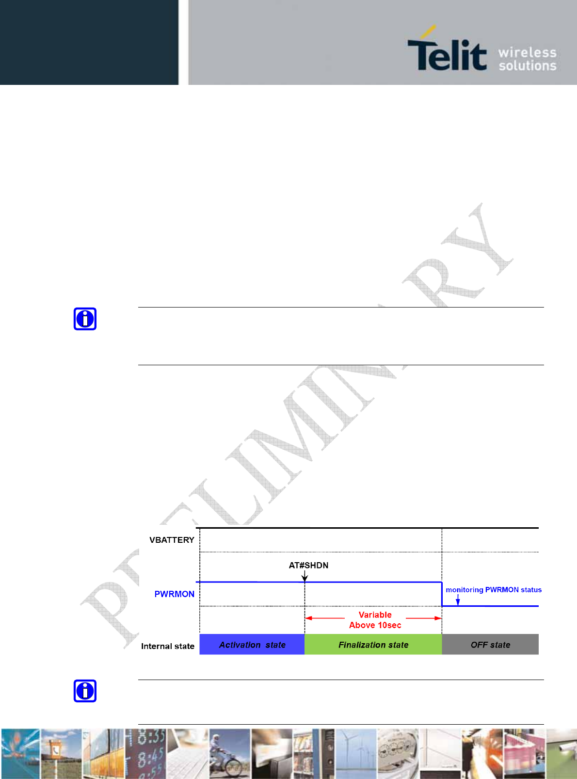
DE910-DUAL can be shut down by a software command.
When a shutdown command is sent, DE910-DUAL goes into the finalization state and finally
will shut down PWRMON at the end of this state.
The period of the finalization state can vary according to the state of the DE910-DUAL so it
cannot be fixed definitely.
Normally it will be above 10 seconds after sending a shutdown command and DTE should
monitor the status of PWRMON to see the actual power off.
TIP:
To check if the device has powered off hardware line PWRMON must be monitored. When
PWRMON goes low, the device has powered off.
HW User Guide Template
1vv0300951 Rev.1 – 2011-12-
Reproduction forbidden without written authorization from Telit Communications S.p.A. - All Rights
Reserved. Page 22 of 60
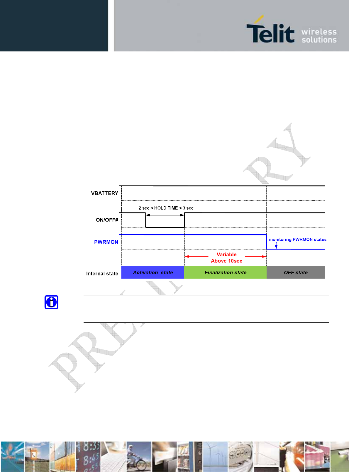
4.2.2. Hardware Shutdown
To turn OFF DE910-DUAL the pad ON/OFF# must be tied low for at least 2 seconds and
then released. The same circuitry and timing for the power on must be used.
When the hold time of ON/OFF# is above 2 seconds, the DE910-DUAL goes into the
finalization state and finally will shut down PWRMON at the end of this state.
The period of the finalization state can vary according to the state of the DE910-DUAL is so
it cannot be fixed definitely.
Normally it will be above 10 seconds after releasing ON/OFF# and DTE should monitor the
status of PWRMON to see the actual power off.
TIP:
To check if the device has powered off, hardware line PWRMON must be monitored. When
PWRMON goes low, the device has powered off.

HW User Guide Template
1vv0300951 Rev.1 – 2011-12-
Reproduction forbidden without written authorization from Telit Communications S.p.A. - All Rights
Reserved. Page 23 of 60
4.2.3. Hardware Unconditional Reboot
To unconditionally restart the DE910-DUAL, the pad RESET# must be tied low for at least
200 milliseconds and then released.
A simple circuit to unconditionally reboot the module is illustrated below:
RESET#
Unconditional Restart
impulse
GND
NOTE:
Do not use any pull up resistor on the RESET# line or any totem pole digital output. Using a
pull up resistor may bring latch up problems on the DE910-DUAL power regulator and
improper functioning of the module. The line RESET# must be connected only in open
collector configuration.
TIP:
The unconditional hardware Restart must always be implemented on the boards and the
software must use it only as an emergency exit procedure.
For example:
Let us assume you need to drive the RESET# pad with a totem pole output of a +1.8/5 V
microcontroller (uP_OUT2):
10k
+1.8 / 5V
HW User Guide Template
1vv0300951 Rev.1 – 2011-12-
Reproduction forbidden without written authorization from Telit Communications S.p.A. - All Rights
Reserved. Page 24 of 60
4.3. Summary of Turning ON and OFF the Module
The chart below describes the overall sequences for turning the module ON and OFF.
HW User Guide Template
1vv0300951 Rev.1 – 2011-12-
Reproduction forbidden without written authorization from Telit Communications S.p.A. - All Rights
Reserved. Page 25 of 60
5. Power Supply
The power supply circuitry and board layout are a very important part in the full product
design and they strongly reflect on the product’s overall performance. Read carefully the
requirements and the guidelines that follow for a proper design.
5.1. Power Supply Requirements
The external power supply must be connected to VBATT & VBATT_PA signals and must
fulfill the following requirements:
Power Supply
Nominal Supply Voltage 3.8V
Max Supply Voltage 4.2V
Supply Voltage Range 3.4V ~ 4.2V
NOTE:
The Operating Voltage Range MUST never be exceeded. Special care must be taken in order
to fulfill min/max supply voltage requirement.
NOTE:
When the power supply voltage is lower than 3.4V, to turn ON the module, the pad ON# must
be tried low for at least 3 seconds.
5.2. General Design Rules
The principal guidelines for the Power Supply Design embrace three different design steps:
• the electrical design
• the thermal design
• the PCB layout
HW User Guide Template
1vv0300951 Rev.1 – 2011-12-
Reproduction forbidden without written authorization from Telit Communications S.p.A. - All Rights
Reserved. Page 26 of 60
5.2.1. Electrical Design Guidelines
The electrical design of the power supply depends strongly on the power source where this
power is drained. We will distinguish them into two categories:
• +5V input (typically PC internal regulator output)
• +12V input (typically automotive)
• Battery
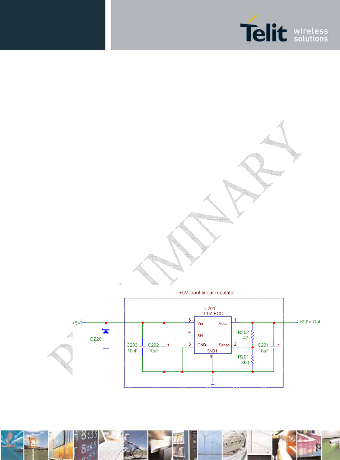
5.2.1.1. + 5V Input Source Power Supply Design Guidelines
• The desired output for the power supply is 3.8V, hence there is not a big
difference between the input source and the desired output so a linear regulator
can be used. A switching power supply will not be suitable because of the low
drop-out requirements.
• When using a linear regulator, a proper heat sink must be provided in order to
dissipate the power generated.
• A Bypass low ESR capacitor of adequate capacity must be provided in order to
cut the current absorption peaks close to the DE910-DUAL. A 100µF tantalum
capacitor is usually suited.
• Make sure the low ESR capacitor on the power supply output (usually a tantalum
one) is rated at least 10V.
• A protection diode must be inserted close to the power input, in order to save
DE910-DUAL from power polarity inversion.
An example of linear regulator with 5V input is:
HW User Guide Template
1vv0300951 Rev.1 – 2011-12-
Reproduction forbidden without written authorization from Telit Communications S.p.A. - All Rights
Reserved. Page 27 of 60
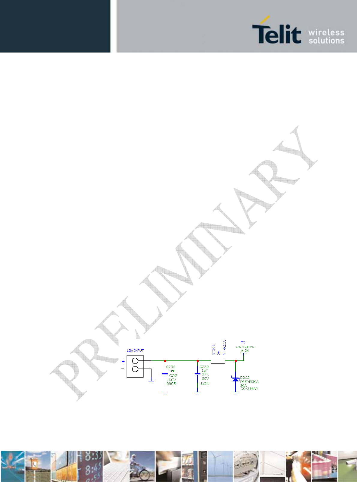
5.2.1.2. +12V Input Source Power Supply Design Guidelines
• The desired output for the power supply is 3.8V, hence due to the big difference
between the input source and the desired output, a linear regulator is not suitable
and must not be used. A switching power supply would be preferable because of
its better efficiency especially with the (TBD) peak current load represented by
DE90-DUAL.
• When using a switching regulator, a 500 kHz or more switching frequency
regulator is preferable because of its smaller inductor size and its faster transient
response. This allows the regulator to respond quickly to the current peaks
absorption.
• In any case, the frequency and switching design selection is related to the
application to be developed due to the fact the switching frequency could also
generate EMC interferences.
• For car PB battery the input voltage can rise up to 15.8V and this must be kept in
mind when choosing components: all components in the power supply must
withstand this voltage.
• A bypass low ESR capacitor of adequate capacity must be provided in order to
cut the current absorption peaks. A 100µF tantalum capacitor is usually suited for
this.
• Make sure the low ESR capacitor on the power supply output (usually a tantalum
one) is rated at least 10V.
• For car applications a spike protection diode must be inserted close to the power
input in order to clean the supply from spikes.
• A protection diode must be inserted close to the power input in order to save
DE910-DUAL from power polarity inversion. This can be the same diode as for
spike protection.
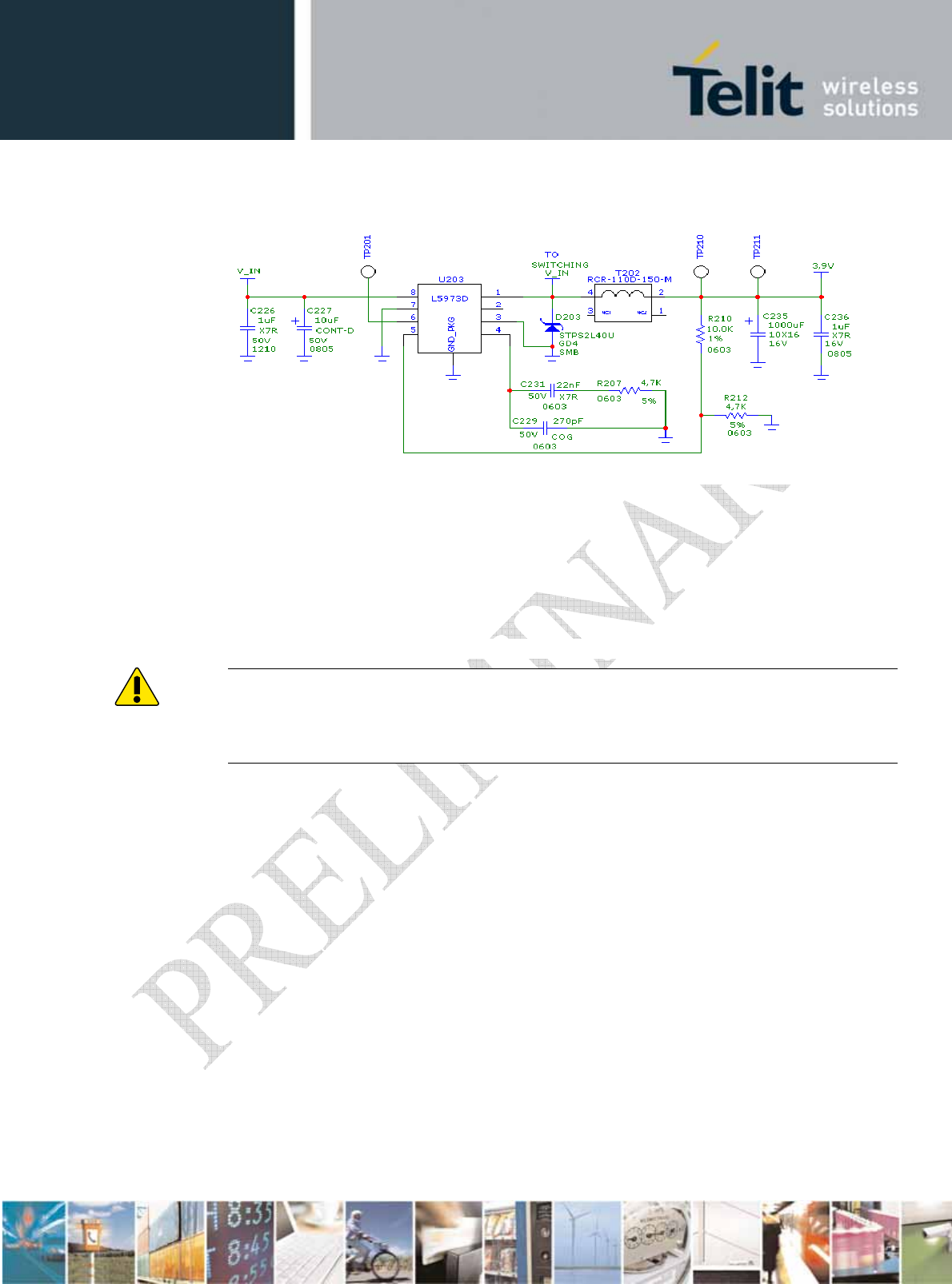
An example of switching regulator with 12V input is in the schematic below (it is split in 2
parts):
HW User Guide Template
1vv0300951 Rev.1 – 2011-12-
Reproduction forbidden without written authorization from Telit Communications S.p.A. - All Rights
Reserved. Page 28 of 60
Switching regulator
5.2.1.3. Battery Source Power Supply Design Guidelines
The desired nominal output for the power supply is 3.8V and the maximum voltage allowed is
4.2V. A single 3.7V lithium-ion cell battery type is ideal to supply the power to the Telit
DE910-DUAL module.
WARNING:
The three battery cells (Ni/Cd or Ni/MH 3.6V nom. battery types or 4V PB types) MUST
NOT be used directly because their maximum voltage can rise over the absolute maximum
voltage for the DE910-DUAL modem and damage it. USE only Li-Ion battery types.
• A bypass low (usually a 100uF tantalum) ESR capacitor with adequate capacity
must be provided in order to cut the current absorption peaks.
• Make sure the low ESR capacitor (usually a tantalum) is rated at least 10V.
• A protection diode must be inserted close to the power input in order to protect
the DE910-DUAL module from power polarity inversions when connecting the
battery.
• The battery capacity must be at least 500mAh in order to withstand the current
peaks of (TBD). The suggested battery capacity is from 500mAh to 1000mAh.
HW User Guide Template
1vv0300951 Rev.1 – 2011-12-
Reproduction forbidden without written authorization from Telit Communications S.p.A. - All Rights
Reserved. Page 29 of 60
5.2.2. Thermal Design Guidelines
The thermal design for the power supply heat sink must be done with the following
specifications:
• Average current consumption during CDMA 1x / 1xEV-DO transmission @PWR
level max : TBD mA
• Average GPS current during GPS ON (Power Saving disabled) in DE910-
DUAL : TBD mA
NOTE:
The average consumption during transmissions depends on the power level at which the
device is requested to transmit via the network. The average current consumption hence varies
significantly.
Considering the very low current during idle, especially if the Power Saving function is
enabled, it is possible to consider from the thermal point of view that the device absorbs
current significantly only during calls.
If we assume that the device stays in transmission for short periods of time (let us say few
minutes) and then remains for quite a long time in idle (let us say one hour), then the power
supply always has the time to cool down between the calls and the heat sink could be smaller
than the calculated for TBD mA maximum RMS current. There could even be a simple chip
package (no heat sink).
Moreover in average network conditions the device is requested to transmit at a lower power
level than the maximum and hence the current consumption will be less than TBD mA (being
usually around TBD mA).
For these reasons the thermal design is rarely a concern and the simple ground plane where
the power supply chip is placed can be enough to ensure a good thermal condition and avoid
overheating.
The heat generated by the DE910-DUAL must be taken into consideration during
transmission at 0.25W max during calls. This generated heat will be mostly conducted to the
ground plane under the DE910-DUAL. The application must be able to dissipate heat.
In the CDMA 1x/1xEV-DO mode, since DE910-DUAL emits RF signals continuously during
transmission, you must pay special attention how to dissipate the heat generated.
The current consumption will be up to about TBD mA in CDMA 1x continuously at the
maximum TX output power (24.5dBm). Thus, you must arrange the area on the application
PCB to be as large as possible under DE910-DUAL.
You must mount DE910-DUAL on the large ground area of your application board and make
many ground vias to dissipate the heat.

HW User Guide Template
1vv0300951 Rev.1 – 2011-12-
Reproduction forbidden without written authorization from Telit Communications S.p.A. - All Rights
Reserved. Page 30 of 60
5.2.3. Power Supply PCB layout Guidelines
As seen in the electrical design guidelines, the power supply must have a low ESR capacitor
on the output to cut the current peaks and a protection diode on the input to protect the supply
from spikes and polarity inversion. The placement of these components is crucial for the
correct operation of the circuitry. A misplaced component can be useless or can even decrease
the power supply performance.
• The bypass low ESR capacitor must be placed close to the Telit DE910-DUAL
power input pads, or if the power supply is a switching type, the capacitor can be
placed close to the inductor to cut the ripple if the PCB trace from the capacitor to
DE910-DUAL is wide enough to ensure a drop-less connection even during the
1A current peaks.
• The protection diode must be placed close to the input connector where the power
source is drained.
• The PCB traces from the input connector to the power regulator IC must be wide
enough to ensure no voltage drops occur when the TBD A current peaks are
absorbed. While a voltage drop of hundreds of mV may be acceptable from the
power loss point of view, the same voltage drop may not be acceptable from the
noise point of view. If your application does not have an audio interface but only
uses the data feature of the Telit DE910-DUAL, then this noise is not as
disturbing and the power supply layout design can be more forgiving.
• The PCB traces to DE910-DUAL and the Bypass capacitor must be wide enough
to ensure no significant voltage drops occur when the TBD A current peaks are
absorbed. This is a must for the same above-mentioned reasons. Try to keep this
trace as short as possible.
• The PCB traces connecting the switching output to the inductor and the switching
diode must be kept as short as possible by placing the inductor and the diode very
close to the power switching IC (only for switching power supply). This is done
in order to reduce the radiated field (noise) at the switching frequency (usually
100-500 kHz).
• The use of a good common ground plane is suggested.
• The placement of the power supply on the board must be done in a way to
guarantee that the high current return paths in the ground plane are not
overlapped to any noise sensitive circuitry such as the microphone
amplifier/buffer or earphone amplifier.
The power supply input cables must be kept separate from noise sensitive lines such as
microphone/earphone cables.

HW User Guide Template
1vv0300951 Rev.1 – 2011-12-
Reproduction forbidden without written authorization from Telit Communications S.p.A. - All Rights
Reserved. Page 31 of 60
6. Antenna (Antenne)
The antenna connection and board layout design are the most important parts in the full
product design and they strongly reflect on the product’s overall performance. Read carefully
and follow the requirements and the guidelines for a proper design.
La connexion de l’antenne ainsi que la conception de la carte sont les parties les plus
importantes du produit et reflètent fortement les performances globales du produit. Lisez
attentivement et suivez les instructions et directives pour une conception appropriée du
produit.
6.1. CDMA Antenna Requirements (Specifications
de l’antenne CDMA)
The antenna for a Telit DE910-DUAL device must fulfill the following requirements:
Comme suggéré sur la description du produit, l'antenne pour un dispositif Telit DE910-
DUAL doit remplir les conditions suivantes:
CDMA Antenna Requirements
Spécification de l' antenne CDMA
Frequency range
Bande de fréquence
Depending on frequency band(s) provided by the network
operator, the customer must use the most suitable antenna for
that/those band(s)
Dépendant des bandes de fréquence fournies par l'opérateur de
réseau, le client doit utiliser l'antenne la plus appropriée pour
celle/ces bandes
Bandwidth
Bande de fréquence
70 MHz in CDMA BC0
140 MHz in CDMA BC1
70 mégahertz dans CDMA BC0
140 mégahertz dans CDMA BC1
Gain
Gain
Gain < 5.12dBi in CDMA BC0
Gain < 6.12dBi in CDMA BC1
Gain<5.12dBi dans CDMA BC0,
Gain<6.12dBi dans CDMA BC1
Impedance
Impédance 50 Ohm
Input power
Puissance d'entrée
> 24dBm Average Power in CDMA
> puissance 24dBm moyenne dans CDMA

HW User Guide Template
1vv0300951 Rev.1 – 2011-12-
Reproduction forbidden without written authorization from Telit Communications S.p.A. - All Rights
Reserved. Page 32 of 60
VSWR absolute max
Maximum absolu de VSWR
≤ 5:1 (Limit to avoid permanent damage)
≤ 5:1 (Limite pour éviter des dommages permanents)
VSWR recommended
VSWRrecommandé
≤ 2:1 (Limit to fulfill all regulatory requirement)
≤ 2:1 (Limite pour remplir toute la condition de normalisation)
When using the Telit DE910-DUAL, since there’s no antenna connector on the module, the
antenna must be connected to the DE910-DUAL antenna pad (K1) by means of a
transmission line implemented in the PCB.
En utilisant le DE910-DUAL Telit, puisqu'il n'y a aucun connecteur d'antenne sur le module,
l'antenne doit être reliée à la plage d’accueil de l'antenne du DE910-DUAL (K1) au moyen
d'une piste de transmission prévue sur la carte.
In the case that the antenna is not directly connected at the antenna pad of the DE910-DUAL,
then a PCB line is required.
Dans le cas où l'antenne n'est pas directement reliée à la plage d’accueil de l'antenne du
DE910-DUAL, alors une piste du PCB est nécessaire afin de se relier à elle ou à son
connecteur.
This transmission line shall fulfill the following requirements:
Cette piste de transmission remplira les conditions suivantes:
Antenna Line on PCB Requirements
Spécification de la piste de l'antenne sur le PCB
Characteristic Impedance
Impédance caractéristique 50Ohm
Max Attenuation
Atténuation maximum 0.3dB
Coupling with other signals shall be avoided
L'accouplement avec d'autres signaux doit être évité
Cold End (Ground Plane) of antenna shall be equipotential to the DE910-DUAL ground
pads
L'extrémité froide (plan de masse) de l'antenne sera équipotentielle aux plages du DE910-
DUAL
Furthermore if the device is developed for the US and/or Canada market, it must comply with
the FCC and/or IC approval requirements:
En outre si le dispositif est développé pour le marché des USA et/ou du Canada, il doit se
conformer aux conditions FCC et/ou IC approuvées:

HW User Guide Template
1vv0300951 Rev.1 – 2011-12-
Reproduction forbidden without written authorization from Telit Communications S.p.A. - All Rights
Reserved. Page 33 of 60
This device is to be used only for mobile and fixed application. The antenna(s) used for this
transmitter must be installed to provide a separation distance of at least 20 cm from all
persons and must not be co-located or operating in conjunction with any other antenna or
transmitter. End-Users must be provided with transmitter operation conditions for satisfying
RF exposure compliance. OEM integrators must ensure that the end user has no manual
instructions to remove or install the DE910-DUAL module. Antennas used for this OEM
module must not exceed 3dBi gain for mobile and fixed operating configurations.
Ce dispositif doit être employé seulement pour une application mobile et fixe. Les antennes
utilisées pour cet émetteur doivent être installées à une distance d’ au moins de 20 cm de toute
personne et ne doivent pas être co-implantées ou opérer en même temps que n'importe quelle
autre antenne ou émetteur. Les conditions de fonctionnement de l’émetteur doivent être
remises aux utilisateurs conformément à la réglementation sur l’exposition aux ondes radio.
Les intégrateurs OEM doivent s'assurer que l'utilisateur n'a aucune instruction manuelle pour
enlever ou installer le module DE910-DUAL. Les antennes utilisées pour ce module OEM ne
doivent pas dépasser un gain de 3dBi pour des configurations mobiles et fixes.
6.2. CDMA antenna – PCB line Guidelines (Antenne
CDMA – Directives pour le PCB)
• Make sure that the transmission line’s characteristic impedance is 50ohm.
Assurez-vous que l'impédance caractéristique de la piste de transmission est 50ohm.
• Keep line on the PCB as short as possible since the antenna line loss shall be less than
around 0.3dB.
Maintenez la piste sur la carte aussi courte que possible, puisque la perte de la piste
d'antenne sera inférieure à 0.3dB.
• Line geometry should have uniform characteristics, constant cross section, avoid
meanders and abrupt curves.
La géométrie de la piste doit avoir des caractéristiques uniformes, une section
transversale constante, évitant les méandres et les courbes brusques.
• Any kind of suitable geometry/structure can be used for implementing the printed
transmission line afferent the antenna.
N'importe quel genre de géométrie/de structure appropriées peut être utilisée pour
mettre en place la piste de transmission afférente à antenne.
• If a Ground plane is required in line geometry, that plane has to be continuous and
sufficiently extended so the geometry can be as similar as possible to the related
canonical model.
Si un plan de masse est exigé ce plan doit être continu et suffisamment étendu afin que
la géométrie soit le plus semblable possible au modèle canonique exposé.
• Keep, if possible, at least one layer of the PCB used only for the Ground plane; If
possible, use this layer as reference Ground plane for the transmission line.
Gardez, si possible, au moins une couche du PCB utilisée uniquement pour le plan de
masse ; Si possible, utilisez cette couche comme plan de masse de référence pour la
piste de transmission.

HW User Guide Template
1vv0300951 Rev.1 – 2011-12-
Reproduction forbidden without written authorization from Telit Communications S.p.A. - All Rights
Reserved. Page 34 of 60
• It is wise to surround (on both sides) of the PCB transmission line with Ground. Avoid
having other signal tracks facing directly the antenna line track.
Il est sage d'entourer (des deux côtés) la piste de transmission du PCB avec la masse, en
évitant d'avoir d'autres pistes de signal faisant face directement à la piste de l'antenne.
• Avoid crossing any un-shielded transmission line footprint with other tracks on
different layers.
Évitez de croiser toute empreinte non protégée avec d’autres pistes sur différentes
couches.
• The Ground surrounding the antenna line on PCB has to be strictly connected to the
main Ground plane by means of via holes (once per 2mm at least) placed close to the
ground edges facing line track.
La masse entourant la piste de l'antenne sur la carte doit être strictement relié au plan de
masse principal par l'intermédiaire de trous (une fois par 2mm au moins), placés près
des bords de la terre faisant face à la piste.
• Place EM noisy devices as far as possible from DE910-DUAL antenna line.
Placez les dispositifs bruyants EM aussi loin que possible de la piste de l’antenne du
DE910-DUAL.
• Keep the antenna line far away from the DE910-DUAL power supply lines.
Maintenez la piste de l'antenne loin des sources d'alimentation du DE910-DUAL.
• If EM noisy devices are present on the PCB hosting the DE910-DUAL, such as fast
switching ICs, take care of shielding them with a metal frame cover.
Si les dispositifs bruyants EM sont présent sur le PCB accueillant le DE910-DUAL, tel
qu’un commutateur rapide IC, prennez soin de le protéger avec un capot métallique.
• If EM noisy devices are not present around the line use of geometries like Micro strip
or Grounded Coplanar Waveguide are preferred since they typically ensure less
attenuation when compared to a Strip line having same length.
Si aucun dispositif bruyant EM n’est présent autour de la piste, l'utilisation de
géométrie comme la bande micro ou le guide d'ondes coplanaire sont recommandés,
puisqu'ils assurent typiquement moins d'atténuation comparé à une bande ayant la
même longueur.
6.3. CDMA Antenna installation Guidelines (Directives
d’installation de l’antenne CDMA)
• Install the antenna in a place covered by the CDMA signal.
Installez l'antenne dans un endroit couvert par le signal CDMA.
• If the device antenna in the application is located greater then 20cm from the human
body and there are no co-located transmitters then the Telit FCC/IC approvals can be
re-used by the end product.
Si le dispositif d'antenne est situé à une distance de plus de 20cm d’une personne et qu’
il n'y a aucun émetteur co-implanté alors les approbations FCC/IC de Telit peuvent être
réutilisées par la produit final.
• Antenna shall not be installed inside metal cases.
L'antenne ne doit pas être installée à l'intérieur de boitiers en métal.
• Antenna shall be installed also according antenna manufacture instructions.
L'antenne doit être installée conformément aux instructions du fabricant.
HW User Guide Template
1vv0300951 Rev.1 – 2011-12-
Reproduction forbidden without written authorization from Telit Communications S.p.A. - All Rights
Reserved. Page 35 of 60
6.4. Antenna Diversity Requirements (Conditions
de diversité d’antenne)
This product is including an input for a second RX antenna to improve the radio sensitivity.
The function is called Antenna Diversity.
Ce produit comprend une deuxième antenne RX pour améliorer la sensibilité. La fonction
s'appelle Antenna Diversity.
CDMA Antenna Diversity Requirements
Conditions de diversité d'antenne CDMA
Frequency range
bande fréquence
Depending on frequency band(s) provided by the network
operator, the customer must use the most suitable antenna for
that/those band(s)
Dépendant des bandes de fréquence fournies par l'opérateur de
réseau, le client doit utiliser l'antenne la plus appropriée pour ces
bandes
Bandwidth
Largeur de bande
70 MHz in CDMA BC0
140 MHz in CDMA BC1
70 mégahertz en CDMA BC0
140 mégahertz en CDMA BC1
Impedance
Impédance 50 Ohm
When using the Telit DE910-DUAL, since there’s no antenna connector on the module, the
antenna must be connected to the DE910-DUAL antenna pad (F1) by means of a transmission
line implemented on the PCB.
En utilisant DE910-DUAL Telit, puisqu'il n'y a aucun connecteur d'antenne sur le module,
l'antenne doit être reliée à la plage d'antenne de DE910-DUAL (F1) par une piste de
transmission prévue sur le PCB.
In the case that the antenna is not directly connected at the antenna pad of DE910-DUAL,
then a PCB line is required.
Dans le cas ou l'antenne n'est pas directement connectée à la plage d'antenne du DE910-
DUAL, alors une psite du PCB est nécessaire afin de se relier à elle ou à son connecteur.
HW User Guide Template
1vv0300951 Rev.1 – 2011-12-
Reproduction forbidden without written authorization from Telit Communications S.p.A. - All Rights
Reserved. Page 36 of 60
6.5. GPS Antenna Requirements
The use of an active GPS antenna is required to achieve better performance especially when
the GPS antenna distance from the module is quite high.
The module is provided with a Digital Output signal to enable the external LNA (pad R7).
6.5.1. Combined GPS Antenna
The use of combined CDMA/GPS antenna is not recommended. This solution could generate
extremely poor GPS reception and also the combined antenna requires additional diplexer and
adds a loss in the RF route.
6.5.2. Linear and Patch GPS Antenna
Using this type of antenna introduces at least 3dB of loss if compared to a circularly polarized
(CP) antenna. Having a spherical gain response instead of a hemispherical gain response
could aggravate the multipath behaviour & create poor position accuracy.
6.5.3. LNA and Front End Design Considerations
The optional external LNA should be dimensioned to avoid an excessive LNA gain that can
introduce jamming, spurious, degrade IIP3, and saturate the receiver.
The external active antenna for the Telit DE910-DUAL device must fulfill the following
requirements:
GPS Antenna Requirements
Frequency range 1575.42MHz (GPS L1)
Bandwidth +/- 1.023MHz
Impedance 50 Ohm
When using the Telit DE910-DUAL, since there’s no antenna connector on the module, the
antenna must be connected to the DE910-DUAL through the PCB with the antenna pad.
In the case that the antenna is not directly connected at the antenna pad of the DE910-DUAL,
then a PCB line is required.
HW User Guide Template
1vv0300951 Rev.1 – 2011-12-
Reproduction forbidden without written authorization from Telit Communications S.p.A. - All Rights
Reserved. Page 37 of 60
This line of transmission shall fulfill the following requirements:
Antenna Line on PCB Requirements
Characteristic Impedance 50Ohm
Max Attenuation 0.3dB
Coupling with other signals shall be avoided
Cold End (Ground Plane) of antenna shall be equipotential to the DE910-DUAL ground
pads
Furthermore if the device is developed for the US and/or Canada market, it must comply with
the FCC and/or IC requirements.
This device is to be used only for mobile and fixed application.
6.5.4. GPS Antenna - PCB Line Guidelines
• Ensure that the antenna line impedance is 50ohm.
• Keep line on the PCB as short as possible to reduce the loss.
• Antenna line must have uniform characteristics, constant cross section, avoid meanders
and abrupt curves.
• Keep one layer of the PCB used only for the Ground plane; if possible.
• Surround (on the sides, over and under) the antenna line on PCB with Ground. Avoid
having other signal tracks directly facing the antenna line track.
• The Ground around the antenna line on PCB has to be strictly connected to the main
Ground plane by placing vias once per 2mm at least.
• Place EM noisy devices as far as possible from DE910-DUAL antenna line.
• Keep the antenna line far away from the DE910-DUAL power supply lines.
• If EM noisy devices are around the PCB hosting the DE910-DUAL, such as fast
switching ICs, take care of shielding of antenna line by burying it inside the layers of
PCB and surround it with Ground planes; or shield it with a metal frame cover.
• If you do not have EM noisy devices around the PCB of DE910-DUAL, use a strip line
on the superficial copper layer for the antenna line. The line attenuation will be lower
than a buried one.
6.5.5. GPS Antenna – Installation Guidelines
• The DE901-DUAL, due to its sensitivity characteristics, is capable of performing a fix
inside buildings. (In any case the sensitivity could be affected by the building
characteristics i.e. shielding)
• The Antenna must not be co-located or operating in conjunction with any other antenna
or transmitter.
• Antenna shall not be installed inside metal cases.
• Antenna shall be installed also according antenna manufacture instructions.
HW User Guide Template
1vv0300951 Rev.1 – 2011-12-
Reproduction forbidden without written authorization from Telit Communications S.p.A. - All Rights
Reserved. Page 38 of 60
7. USB Port
The DE910-DUAL module includes a Universal Serial Bus (USB) transceiver, which
operates at USB low-speed (1.5Mbits/sec), USB full-speed (12Mbits/sec) and USB high-
speed (480Mbits/sec).
It is compliant with the USB 2.0 specification and can be used for diagnostic monitoring,
control and data transfers.
The table below describes the USB interface signals:
PAD Signal I/O Function Type COMMENT
B15 USB D+ I/O USB differential Data (+) 1.8V
C15 USB_D- I/O USB differential Data (-) 1.8V
A13 USB_VBUS AI Power sense for the internal USB
transceiver. 5V
The USB_DPLUS and USB_DMINUS signals have a clock rate of 480MHz. The signal
traces should be routed carefully. Trace lengths, number of vias and capacitive loading should
be minimized. The impedance value should be as close as possible to 90 Ohms differential.
HW User Guide Template
1vv0300951 Rev.1 – 2011-12-
Reproduction forbidden without written authorization from Telit Communications S.p.A. - All Rights
Reserved. Page 39 of 60
8. SPI Port (TBD)
The DE910-DUAL module is provided by one SPI interface. The SPI interface defines one
handshake line for flow control and mutual wake-up of the modem and the Application
Processor. The AP has the master role, that is, it supplies the clock.
The following table is listing the available signals:
PAD Signal I/O Function Type COMMENT
D15 SPI_MOSI I SPI_MOSI B-PD
1.8V Shared with TX_AUX
E15 SPI_MISO O SPI_MISO B-PD
1.8V Shared with RX_AUX
F15 SPI_CLK I SPI_CLOCK B-PD
1.8V
H14 SPI_CS_N I SPI_CS_N B-PD
1.8V
NOTE:
Due to shared functions, when the SPI port is used, it is not possible to use the AUX_UART
function.
8.1. SPI Connections
DE910-DUAL AP
D15
E15
F15
H14
SPI_MOSI
SPI_MISO
SPI_CLK
SPI_CS_N
ESD Protection

HW User Guide Template
1vv0300951 Rev.1 – 2011-12-
Reproduction forbidden without written authorization from Telit Communications S.p.A. - All Rights
Reserved. Page 40 of 60
9. Serial Port
The serial port on the Telit DE910-DUAL is the interface between the module and OEM
hardware.
2 serial ports are available on the module:
• Modem Serial Port 1 (Main)
• Modem Serial Port 2 (Auxiliary)
Several configurations can be designed for the serial port on the OEM hardware.
The most common are:
• RS232 PC comport
• Microcontroller UART@1.8V(Universal Asynchronous Receiver Transmit)
• Microcontroller UART@5V or other voltages different from 1.8V
Depending on the type of serial port on the OEM hardware, a level translator circuit may be
needed to make the system work.
Serial port 1 on DE910-DUAL is a +1.8V UART with all the 7 RS232 signals.
Serial port 2 is a +1.8V Auxiliary UART.
The electrical characteristics of the Serial ports are explained in the following tables:
Absolute Maximum Ratings -Not Functional
Parameter DE910-DUAL
Min Max
Input level on non-power pin with respect to ground - +2.3V
Operating Range - Interface levels
Level DE910-DUAL
Min Max
Input high level 1.17V 2.1 V
Input low level -0.3V 0.63V
Output high level 1.35V 1.8V
Output low level 0V 0.45V
HW User Guide Template
1vv0300951 Rev.1 – 2011-12-
Reproduction forbidden without written authorization from Telit Communications S.p.A. - All Rights
Reserved. Page 41 of 60
9.1. Modem Serial Port 1
The serial port 1 on the DE910-DUAL is a +1.8V UART with all the 7 RS232 signals.
It differs from the PC-RS232 in the signal polarity (RS232 is reversed) and levels.
PAD Signal I/O Function Type COMMENT
N14 DCD -
dcd_uart Data Carrier Detect B-PU
1.8V
M15 RXD -
Tx_uart Transmit line *see Note B-PD
1.8V
N15 TXD -
Rx_uart Receive line *see Note B-PD
1.8V
M14 DTR -
dtr_uart Data Terminal Ready B-PU
1.8V
P14 DSR -
dsr_uart Data Set Ready B-PU
1.8V
L14 RTS -
rts_uart Request to Send B-PD
1.8V
P15 CTS -
cts_uart Clear to Send B-PD
1.8V
R14 RI -
ri_uart Ring Indicator B-PU
1.8V
NOTE:
For minimum implementation, only the TXD and RXD lines must be connected, the other
lines can be left open provided a software flow control is implemented.
NOTE:
In order to avoid a back powering effect it is recommended to avoid having any HIGH logic
level signal applied to the digital pins of the DE910-DUAL when the module is powered off
or during an ON/OFF transition.
NOTE:
According to V.24, RX/TX signal names are referred to the application side. Therefore, on the
DE910-DUAL side these signal are on the opposite direction: TXD on the application side
will be connected to the receive line (here named TXD/ rx_uart ) of the DE910-DUAL serial
port and vice versa for RX.
HW User Guide Template
1vv0300951 Rev.1 – 2011-12-
Reproduction forbidden without written authorization from Telit Communications S.p.A. - All Rights
Reserved. Page 42 of 60
9.2. Modem Serial Port 2
Serial port 2 on the DE910-DUAL is a +1.8V UART with only the RX and TX signals.
The signals of the DE910-DUAL serial port are:
PAD Signal I/O Function Type COMMENT
D15 TX_AUX O Auxiliary UART (TX Data to DTE) 1.8V Shared with SPI_MOSI
E15 RX_AUX I Auxiliary UART (RX Data to DTE) 1.8V Shared with SPI_MISO
NOTE:
Due to the shared pins, when the Modem Serial port is used, it is not possible to use the SPI
functions.
NOTE:
In order to avoid a back powering effect it is recommended to avoid having any HIGH logic
level signal applied to the digital pins of the DE910-DUAL when the module is powered off
or during an ON/OFF transition.
9.3. RS232 Level Translation
In order to interface the Telit DE910-DUAL with a PC com port or a RS232 (EIA/TIA-232)
application, a level translator is required. This level translator must:
• Invert the electrical signal in both directions
• Change the level from 0/1.8V to +/-15V
Actually, the RS232 UART 16450, 16550, 16650 & 16750 chipsets accept signals with lower
levels on the RS232 side (EIA/TIA-562), allowing a lower voltage-multiplying ratio on the
level translator. Note that the negative signal voltage must be less than 0V and hence some
sort of level translation is always required.
The simplest way to translate the levels and invert the signal is by using a single chip level
translator. There are a multitude of them, differing in the number of drivers and receivers and
in the levels (be sure to get a true RS232 level translator not a RS485 or other standards).
By convention the driver is the level translator from the 0-1.8V UART to the RS232 level.
The receiver is the translator from the RS232 level to 0-1.8V UART.
In order to translate the whole set of control lines of the UART you will need:
• 5 drivers
• 3 receivers
HW User Guide Template
1vv0300951 Rev.1 – 2011-12-
Reproduction forbidden without written authorization from Telit Communications S.p.A. - All Rights
Reserved. Page 43 of 60
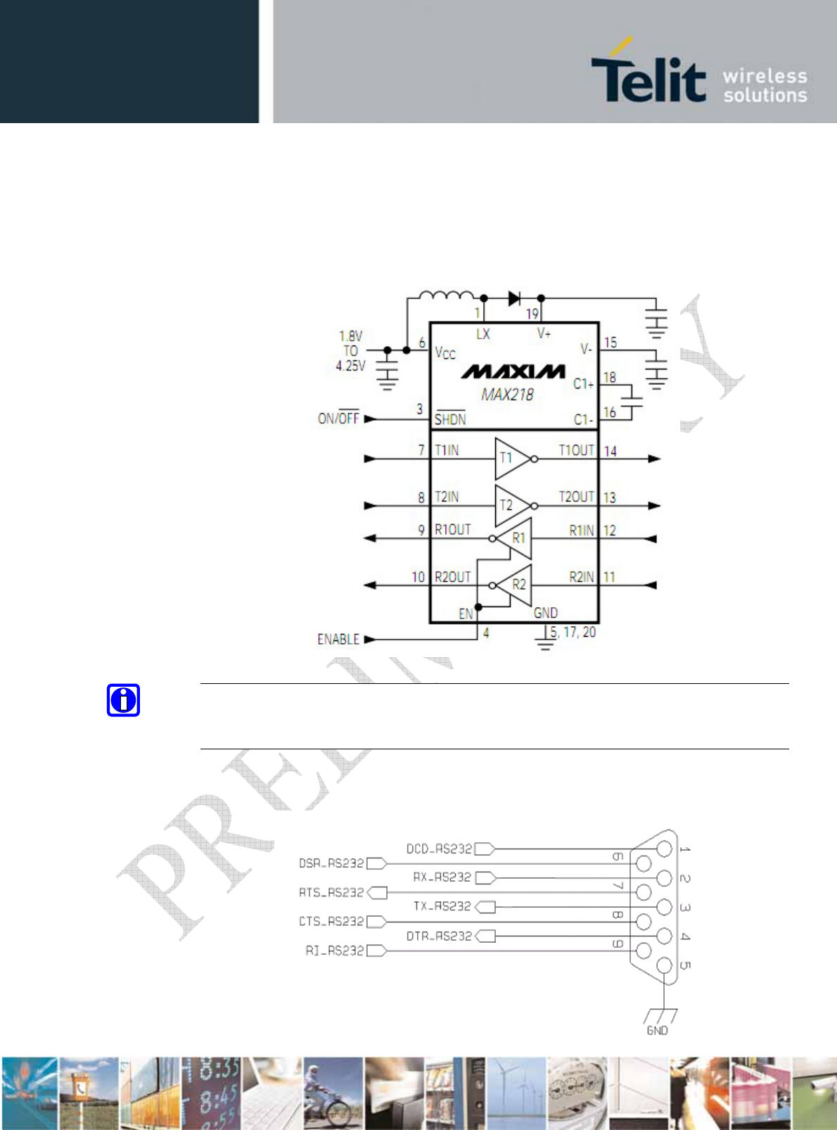
An example of RS232 level adaption circuitry could be accomplished using a MAXIM
transceiver (MAX218).
In this case the chipset is capable of translating directly from 1.8V to the RS232 levels
(Example on 4 signals only).
NOTE:
In this case the length of the lines on the application has to be taken in account to avoid
problems in case of High-speed rates on RS232.
The RS232 serial port lines are usually connected to a DB9 connector with the following
layout:
HW User Guide Template
1vv0300951 Rev.1 – 2011-12-
Reproduction forbidden without written authorization from Telit Communications S.p.A. - All Rights
Reserved. Page 44 of 60
10. Audio Section Overview
DE910-DUAL module doesn’t support an analog audio interface and supports one Digital
Audio bus.
In order to develop an application including an Analog Audio it is necessary to add a
dedicated CODEC on the Application design.
For further information, please refer to the “Digital Voice Interface Application Note (TBD)”.
10.1. Electrical Characteristics
The product is providing one Digital Audio Interface (DVI) on the following Pins:
PAD Signal I/O Function Type COMMENT
B9 DVI_WA0 I/O Digital Audio Interface (WA0) B-PD
1.8V
B6 DVI_RX I Digital Audio Interface (RX) B-PD
1.8V
B7 DVI_TX O Digital Audio Interface (TX) B-PD
1.8V
B8 DVI_CLK I/O Digital Audio Interface (CLK) B-PD
1.8V
10.1.1. CODEC Example
Please refer to the Digital Voice Interface Application note. (TBD)
HW User Guide Template
1vv0300951 Rev.1 – 2011-12-
Reproduction forbidden without written authorization from Telit Communications S.p.A. - All Rights
Reserved. Page 45 of 60
11. General Purpose I/O
The general-purpose I/O pads can be configured to act in three different ways:
• Input
• Output
• Alternate function (internally controlled)
Input pads can only be read and report the digital value (high or low) present on the pad at the
read time;
Output pads can only be written or queried and set the value of the pad output;
An alternate function pad is internally controlled by the DE9109-DUAL firmware and acts
depending on the function implemented.
The following GPIOs are available on the DE910-DUAL.
PAD Signal I/O Function Type Drive Strength
C8 GPIO_01 I/O Configurable GPIO B-PD
1.8V 2 mA
C9 GPIO_02 I/O Configurable GPIO B-PD
1.8V 2 mA
C10 GPIO_03 I/O Configurable GPIO B-PD
1.8V 2 mA
C11 GPIO_04 I/O Configurable GPIO B-PD
1.8V 2 mA
B14 GPIO_05 I/O Configurable GPIO B-PD
1.8V 2 mA
C12 GPIO_06 I/O Configurable GPIO B-PD
1.8V 2 mA
C13 GPIO_07 I/O Configurable GPIO B-PD
1.8V 2 mA
K15 GPIO_08 I/O Configurable GPIO B-PD
1.8V 2 mA
L15 GPIO_09 I/O Configurable GPIO B-PD
1.8V 2 mA
G15 GPIO_10 I/O Configurable GPIO B-PD
1.8V 2 mA
HW User Guide Template
1vv0300951 Rev.1 – 2011-12-
Reproduction forbidden without written authorization from Telit Communications S.p.A. - All Rights
Reserved. Page 46 of 60
11.1. Logic Level Specification
Where not specifically stated, all the interface circuits work at 1.8V CMOS logic levels.
The following table shows the logic level specifications used in the DE910-DUAL interface
circuits:
Operating Range - Interface levels (1.8V CMOS)
Level DE910-DUAL
Min Max
Input high level 1.17V 2.1V
Input low level -0.3V 0.63V
Output high level 1.35V 1.8V
Output low level 0V 0.45V
11.2. Using a GPIO Pad as Input
The GPIO pads, when used as inputs, can be connected to a digital output of another device
and report its status, provided this device has interface levels compatible with the 1.8V
CMOS levels of the GPIO.
If the digital output of the device is connected with the GPIO input, the pad has interface
levels different from the 1.8V CMOS. It can be buffered with an open collector transistor with
a 47KΩ pull-up resistor to 1.8V.
NOTE:
In order to avoid a back powering effect it is recommended to avoid having any HIGH logic
level signal applied to the digital pins of the module when is powered OFF or during an
ON/OFF transition.
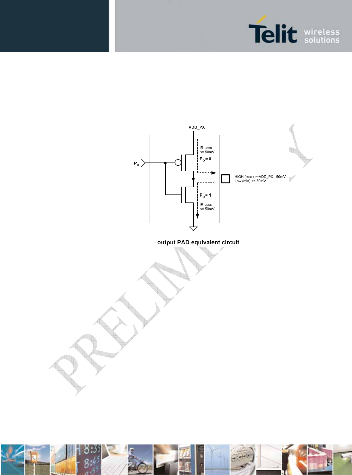
HW User Guide Template
1vv0300951 Rev.1 – 2011-12-
Reproduction forbidden without written authorization from Telit Communications S.p.A. - All Rights
Reserved. Page 47 of 60
11.3. Using a GPIO Pad as Output
The GPIO pads, when used as outputs, can drive 1.8V CMOS digital devices or compatible
hardware. When set as outputs, the pads have a push-pull output and therefore the pull-up
resistor may be omitted.
11.4. Using the Temperature Monitor Function
(TBD)
11.4.1. Short Description
The Temperature Monitor is a function of the module that permits to control its internal
temperature and if properly set (see the #TEMPMON command on AT Interface guide) raises
to High Logic level a GPIO when the maximum temperature is reached.
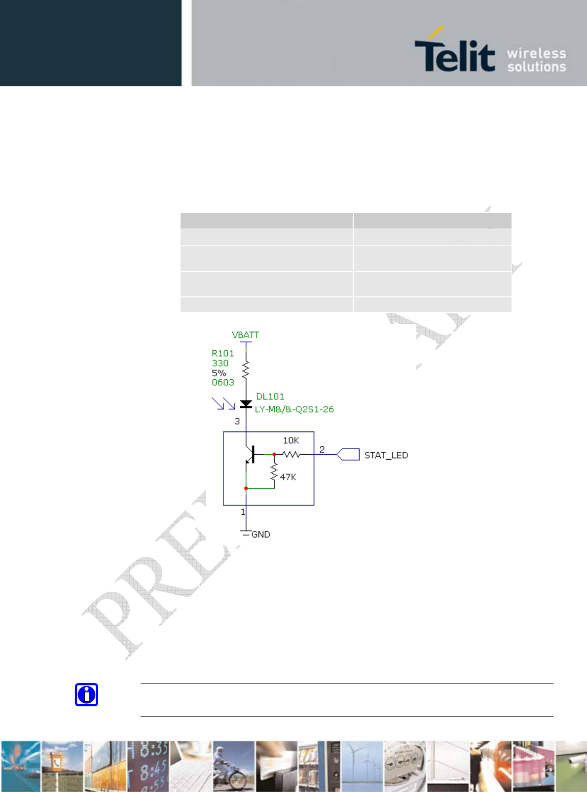
HW User Guide Template
1vv0300951 Rev.1 – 2011-12-
Reproduction forbidden without written authorization from Telit Communications S.p.A. - All Rights
Reserved. Page 48 of 60
11.5. Indication of Network Service Availability
The STAT_LED pin status shows information on the network service availability and Call
status. In the DE910-DUAL modules, the STAT_LED usually needs an external transistor to
drive an external LED. Because of the above, the status indicated in the following table is
reversed with respect to the pin status:
LED status Device Status
Permanently off Device off
Fast blinking
(Period 1s, Ton 0,5s)
Net search / Not registered /
turning off
Slow blinking
(Period 3s, Ton 0,3s)
Registered full service
Permanently on a call is active
11.6. RTC Bypass output
The VRTC pin brings out the Real Time Clock supply, which is separate from the rest of the
digital part, allowing only RTC to be active when all the other parts of the device are off. To
this power output a backup capacitor can be added in order to increase the RTC autonomy
during power off of the battery.
NOTE:
NO devices must be powered from this pin.
HW User Guide Template
1vv0300951 Rev.1 – 2011-12-
Reproduction forbidden without written authorization from Telit Communications S.p.A. - All Rights
Reserved. Page 49 of 60
11.7. VAUX/PWRMON Power Output
A regulated power supply output is provided in order to supply small devices from the
module. This output is active when the module is ON and goes OFF when the module is shut
down. The operating range characteristics of the supply are:
Operating Range – VAUX/PWRMON power supply
Min Typical Max
Output voltage V 1.8V V
Output current 200mA
Output bypass capacitor
(Inside the module) 1.0µF
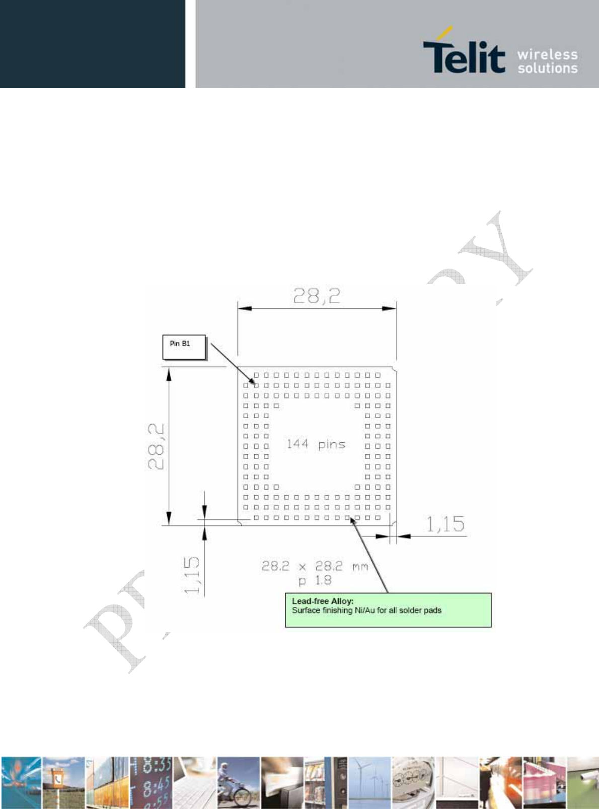
HW User Guide Template
1vv0300951 Rev.1 – 2011-12-
Reproduction forbidden without written authorization from Telit Communications S.p.A. - All Rights
Reserved. Page 50 of 60
12. Mounting the Module on your Board
12.1. General
The DE910-DUAL modules have been designed in order to be compliant with a standard
lead-free SMT process.
12.2. Module Finishing & Dimensions
Bottom View (Dimensions in mm)
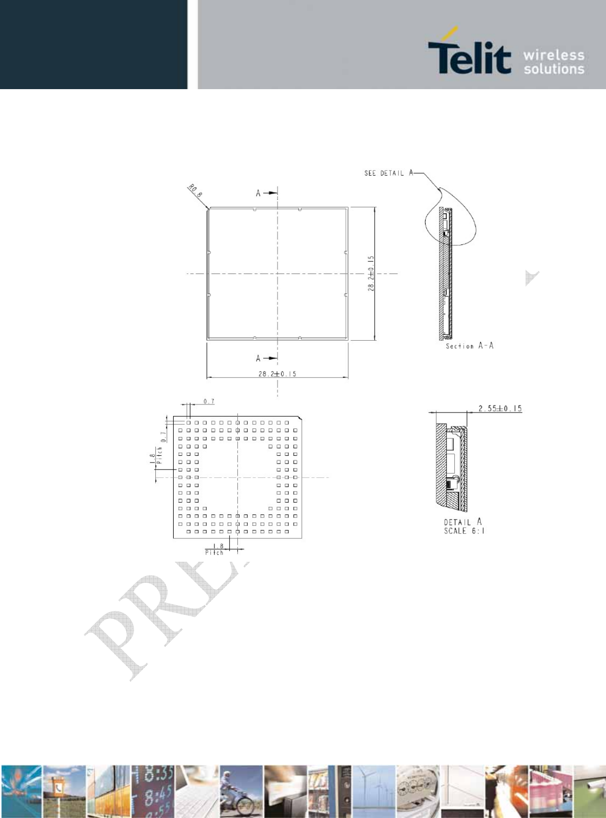
HW User Guide Template
1vv0300951 Rev.1 – 2011-12-
Reproduction forbidden without written authorization from Telit Communications S.p.A. - All Rights
Reserved. Page 51 of 60
12.3. DE910-DUAL Mechanical Dimensions
(Dimensions in mm)
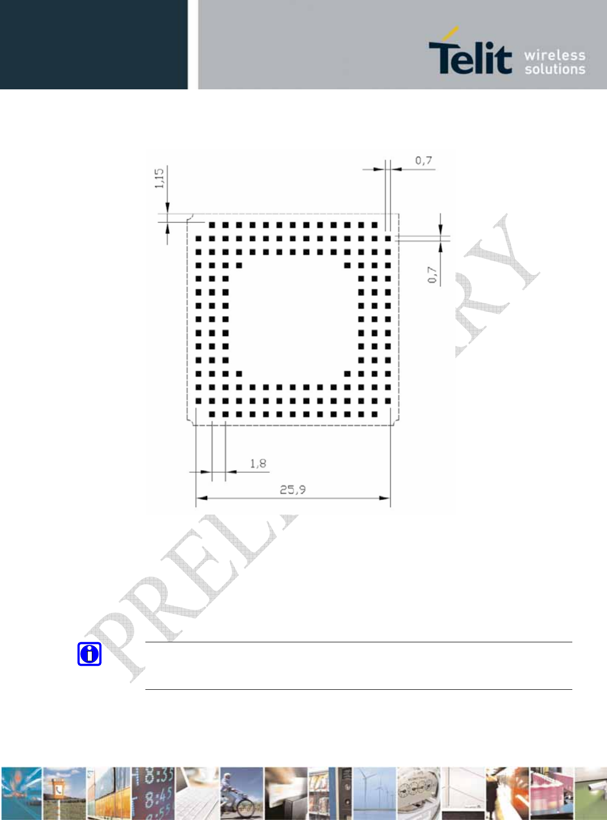
HW User Guide Template
1vv0300951 Rev.1 – 2011-12-
Reproduction forbidden without written authorization from Telit Communications S.p.A. - All Rights
Reserved. Page 52 of 60
12.4. Recommended foot print for the application
Top View
In order to easily rework the DE910-DUAL it is suggested to consider on the application
having a 1.5 mm placement inhibit area around the module.
It is also suggested, as common rule for an SMT component, to avoid having a mechanical
part of the application in direct contact with the module.
NOTE:
In the customer application, the region under WIRING INHIBIT (see figure) must be clear
from signal or ground paths.
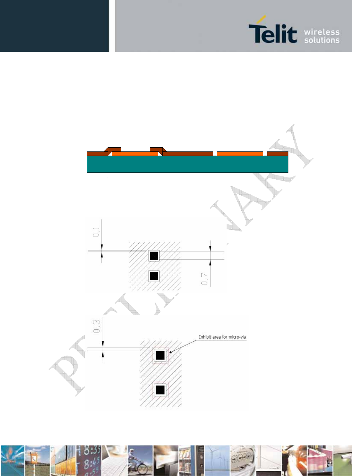
HW User Guide Template
1vv0300951 Rev.1 – 2011-12-
Reproduction forbidden without written authorization from Telit Communications S.p.A. - All Rights
Reserved. Page 53 of 60
12.5. Stencil
Stencil’s apertures layout can be the same of the recommended footprint (1:1). A suggested
thickness of stencil foil is less than 120 µm.
12.6. PCB Pad Design
Non solder mask defined (NSMD) type is recommended for the solder pads on the PCB.
PCB
Solder maskCopper pad
Solder Mask Defined
Copper pad
Non Solder Mask Defined
12.7. Recommendations for PCB Pad Dimensions mm)
It is not recommended to place via or micro-via not covered by solder resist in an area of 0,3
mm around the pads unless it carries the same signal of the pad itself (see following figure).
Holes in pad are allowed only for blind holes and not for through holes.
HW User Guide Template
1vv0300951 Rev.1 – 2011-12-
Reproduction forbidden without written authorization from Telit Communications S.p.A. - All Rights
Reserved. Page 54 of 60
12.8. Recommendations for PCB Pad Surfaces
Finish Layer thickness (um) Properties
Electro-less Ni / Immersion Au 3 –7 / 0.05 – 0.15 good solder ability protection,
high shear force values
The PCB must be able to resist the higher temperatures which are occurring at the lead-free
process. This issue should be discussed with the PCB-supplier. Generally, the wettability of
tin-lead solder paste on the described surface plating is better compared to lead-free solder
paste.
12.9. Solder Paste
Solder Paste Lead free
Sn/Ag/Cu
We recommend useing only “no clean” solder paste in order to avoid the cleaning of the
modules after assembly.
12.10. Solder Reflow
The following is the recommended solder reflow profile:
Profile stage Description Leed-free(High-Temp)
condition limits
Preheat Initial ramp 3 ℃/sec max
Soak Dry out and flux activation 135 to 175 ℃
60 to 120 sec
Reflow Time above solder paste melting point 40 to 90 sec
SMT peak package body temperature 245 ℃
Cool down Cool rate-ramp to ambient 6 ℃/sec max
NOTE:
All temperatures refer to topside of the package, measured on the package body surface.
WARNIG:
The DE910-DUAL module withstands one reflow process only.
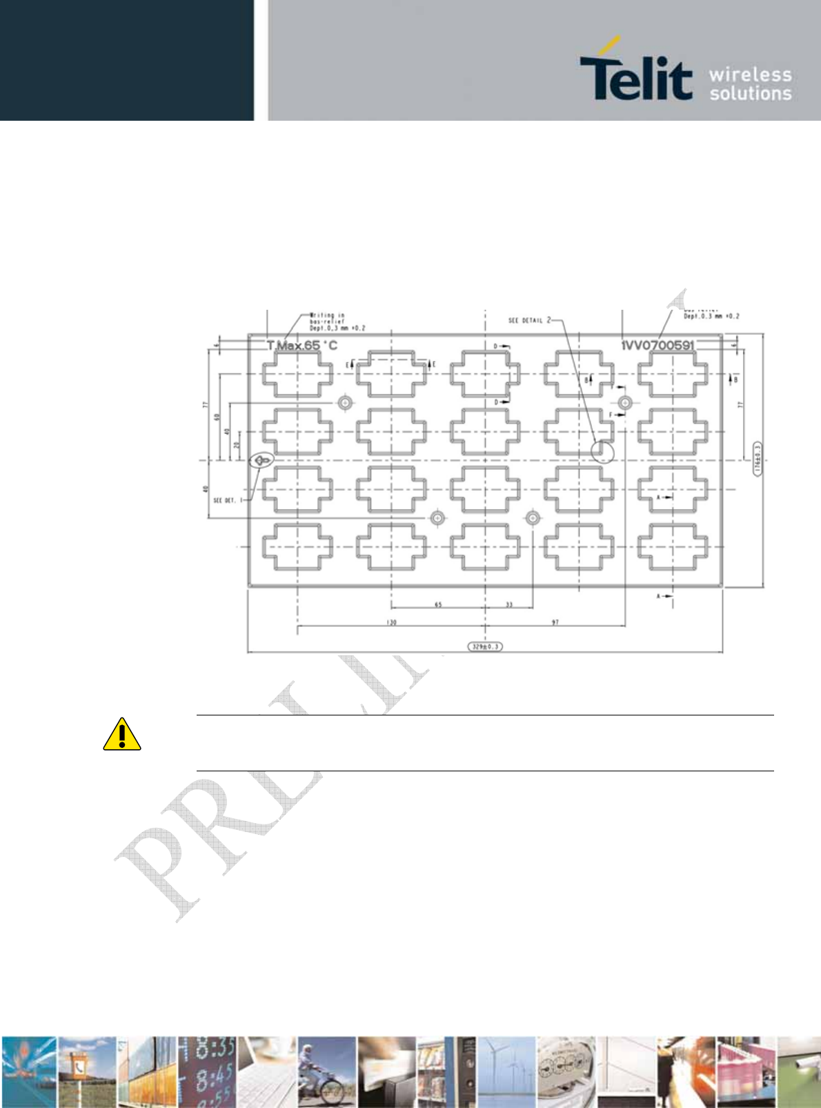
HW User Guide Template
1vv0300951 Rev.1 – 2011-12-
Reproduction forbidden without written authorization from Telit Communications S.p.A. - All Rights
Reserved. Page 55 of 60
12.11. Packing System
The DE910-DUAL modules are packaged on trays of 20 pieces each. These trays can be used
in SMT processes for pick & place handling.
12.11.1. Tray Drawing
(1VV0700591-0A)
WARNIG:
These trays can withstand a maximum temperature of 65℃.
12.12. Moisture Sensibility
The DE910-DUAL is a Moisture Sensitive Device level 3, in accordance with standard
IPC/JEDEC J-STD-020. Observe all of the requirements for using this kind of components.
Calculated shelf life in sealed bag: 4 months at <40°C and <90% relative humidity (RH).

HW User Guide Template
1vv0300951 Rev.1 – 2011-12-
Reproduction forbidden without written authorization from Telit Communications S.p.A. - All Rights
Reserved. Page 56 of 60
13. Conformity Assessment Issues (Problèmes
d'évaluation de conformité)
The DE910-DUAL is FCC/IC Approved as module to be installed in other devices. This
device should be used only for fixed and mobile applications and if the final product after
integration is intended for portable use, a new application and FCC is required.
Le DE910-DUAL est approuvé FCC/IC comme module à installer dans d'autres dispositifs.
Ce dispositif doit être utilisé uniquement pour des applications fixes et mobiles et si le
produit fini est prévu après intégration pour un usage portatif, une nouvelle application et la
FCC est requise
The user is cautioned that this device should be used only as specified within this manual to
meet RF exposure requirements.
L'utilisateur est averti que ce dispositif doit être utilisé uniquement comme spécifié dans ce
manuel pour répondre aux normes d'exposition aux ondes rf.
Use of this device in a manner inconsistent with this manual could lead to excessive RF
exposure conditions.
L'utilisation de ce dispositif en quelque sorte contradictoire avec ce manuel a pu mener aux
états excessifs d'exposition de rf.
The DE910-DUAL is conforming to the following US Directives:
• Use of RF Spectrum. Standards: FCC47 Part 22&24
• EMC Standards: FCC47 Part 15
Le DE910-DUAL est conforme aux directives suivantes des USA
• Utilisation de spectre de rf. Normes : FCC47 partie 22&24
• Normes d'EMC : FCC47 partie 15
This device complies with Part 15 of the FCC Rules.
Ce dispositif est conforme à la partie 15 des règles FCC.
Operation is subject to the following two conditions:
(1) This device may not cause harmful interference, and
(2) This device must accept any interference, including interference that may cause
undesired operation of the device.
Le fonctionnement est sujet aux deux conditions suivantes :
(1) ce dispositif peut ne pas causer l'interférence nocive, et
(2) ce dispositif doit accepter aucune interférence, y compris un interférence qui
pourrait causer le fonctionnement non désiré du dispositif.

HW User Guide Template
1vv0300951 Rev.1 – 2011-12-
Reproduction forbidden without written authorization from Telit Communications S.p.A. - All Rights
Reserved. Page 57 of 60
The user must refer to below information to meet the FCC/IC's RF exposure rules and
regulations when they design:
Lors de la conception, l'utilisateur doit se référer à l'information ci-dessous pour remplir les
conditions et règlementations FCC/IC' d’exposition aux ondes RF:
• The system antenna(s) used for this transmitter must be installed to provide a
separation distance of at least 20 cm from all the persons and must not be co-located
or operating in conjunction with any other antenna or transmitter.
Le système d’antenne utilisé pour cet émetteur doit être installé à une distance d’au
moins de 20 cm de toute personne et ne doit pas être co-implanté ou opérer en même
temps que n'importe quelle autre antenne ou émetteur.
• The system antenna(s) used for this module must not exceed 5.12dBi in CDMA BC0
and 6.12dBi in CDMA BC1 for mobile and fixed or mobile operating configurations.
Le système d’ antenne utilisé pour ce module ne doit pas dépasser 5.12dBi en
CDMA BC0 et 6.12dBi en CDMA BC1 pour des configurations mobiles et fixes ou
des configurations opérant en mode mobile.
• Users and installers must be provided with antenna installation instructions and
transmitter operating conditions for satisfying RF exposure compliance.
Manufacturers of mobile, fixed or portable devices incorporating this module are
advised to clarify any regulatory questions and to have their complete product tested
and approved for FCC compliance.
Les instructions d’installation de l’antenne ainsi que les conditions de
fonctionnement de l’émetteur doivent être remis aux utilisateurs et aux installateurs
conformément à la règlementation sur l’exposition aux ondes rf. Des fabricants des
dispositifs mobiles, fixes ou portables incorporant ce module sont invités à clarifier
toutes les questions de normalisation et à avoir leur produit complètement testé pour
la mise en conformité FCC.
• DE910-DUAL is intended for the OEM integrator only.
DE910-DUAL est prévu pour l'intégrateur OEM seulement.
• The user is required to see the Grant of Equipment document for other restrictions.
L'utilisateur doit se referrer au document « Grant of equipment » pour d'autres
restrictions.
• DE910-DUAL must be operated and used with a locally approved access point.
DE910-DUAL doit être actionné et utilisé avec un point d'accès localement approuvé.
• The radio transmitter(IC ID: 5131A-DE910DUAL) has been approved by Industry
Canada to operate with the antenna type listed in this manual with the maximum
permissible gain and required antenna impedance for each antenna type indicated.
Antenna types not included in this list, having a gain greater than the maximum gain
indicated for that type, are strictly prohibited for use with this device.
L'émetteur radio (identification d'IC : 5131A-DE910DUAL) a été approuvé par
Industry Canada pour fonctionner avec le type d'antenne énuméré dans ce manuel
avec le gain autorisé maximum et l'impédance d’antenne exigée pour chaque type
d'antenne indiqué. Les types d'antenne non inclus dans cette liste, ayant un gain
supérieur au gain maximum indiqué pour ce type, sont strictement interdits pour un
usage avec ce dispositif.

HW User Guide Template
1vv0300951 Rev.1 – 2011-12-
Reproduction forbidden without written authorization from Telit Communications S.p.A. - All Rights
Reserved. Page 58 of 60
The following regulatory and safety notices must be published in documentation supplied
to the end user of the product or system incorporating an adapter in compliance with local
regulations.
• Host system including DE910-DUAL must be labeled with
“Contains transmitter module with
FCC ID: RI7DE910-DUAL and IC ID: 5131A-DE910DUAL”
Les notices de normalisation et de sécurité doivent se trouver dans la documentation
fournie à l'utilisateur du produit ou du système incorporant un adaptateur conforme aux
règlementations locales.
• Le système hôte comprenant DE910-DUAL doit être marqué avec « Contient un
module émetteur avec IDENTIFICATION FCC : RI7DE910-DUAL et
identification IC : 5131A-DE910DUAL »

HW User Guide Template
1vv0300951 Rev.1 – 2011-12-
Reproduction forbidden without written authorization from Telit Communications S.p.A. - All Rights
Reserved. Page 59 of 60
14. Safety Recommendations
READ CAREFULLY
Be sure the use of this product is allowed in the country and in the environment required. The
use of this product may be dangerous and has to be avoided in the following areas:
• Where it can interfere with other electronic devices in environments such as hospitals,
airports, aircrafts, etc.
• Where there is risk of explosion such as gasoline stations, oil refineries, etc. It is the
responsibility of the user to enforce the country’s regulations and the specific
environment regulation.
Do not disassemble the product; any evidence of tampering will compromise the warranty
validity. We recommend following the instructions of the hardware user guides for a correct
wiring of the product. The product has to be supplied with a stabilized voltage source and the
wiring has to be conforming to the security and fire prevention regulations. The product has to
be handled with care, avoiding any contact with the pins because electrostatic discharges may
damage the product itself.
The system integrator is responsible for the functioning of the final product; therefore, care
has to be taken with the external components of the module, as well as of any project or
installation issue, because the risk of disturbing the CDMA network or external devices or
having impact on security. Should there be any doubt, please refer to the technical
documentation and the regulations in force. Every module has to be equipped with a proper
antenna with specific characteristics. The antenna has to be installed with care in order to
avoid any interference with other electronic devices and has to guarantee a minimum distance
from the body (20 cm). In case this requirement cannot be satisfied, the system integrator has
to assess the final product against the SAR regulation.
HW User Guide Template
1vv0300951 Rev.1 – 2011-12-
Reproduction forbidden without written authorization from Telit Communications S.p.A. - All Rights
Reserved. Page 60 of 60
15. Document History
Revision Date Changes
0 2011-11-30 Release for SFN samples
1 2011-12-09 Release for Beta samples