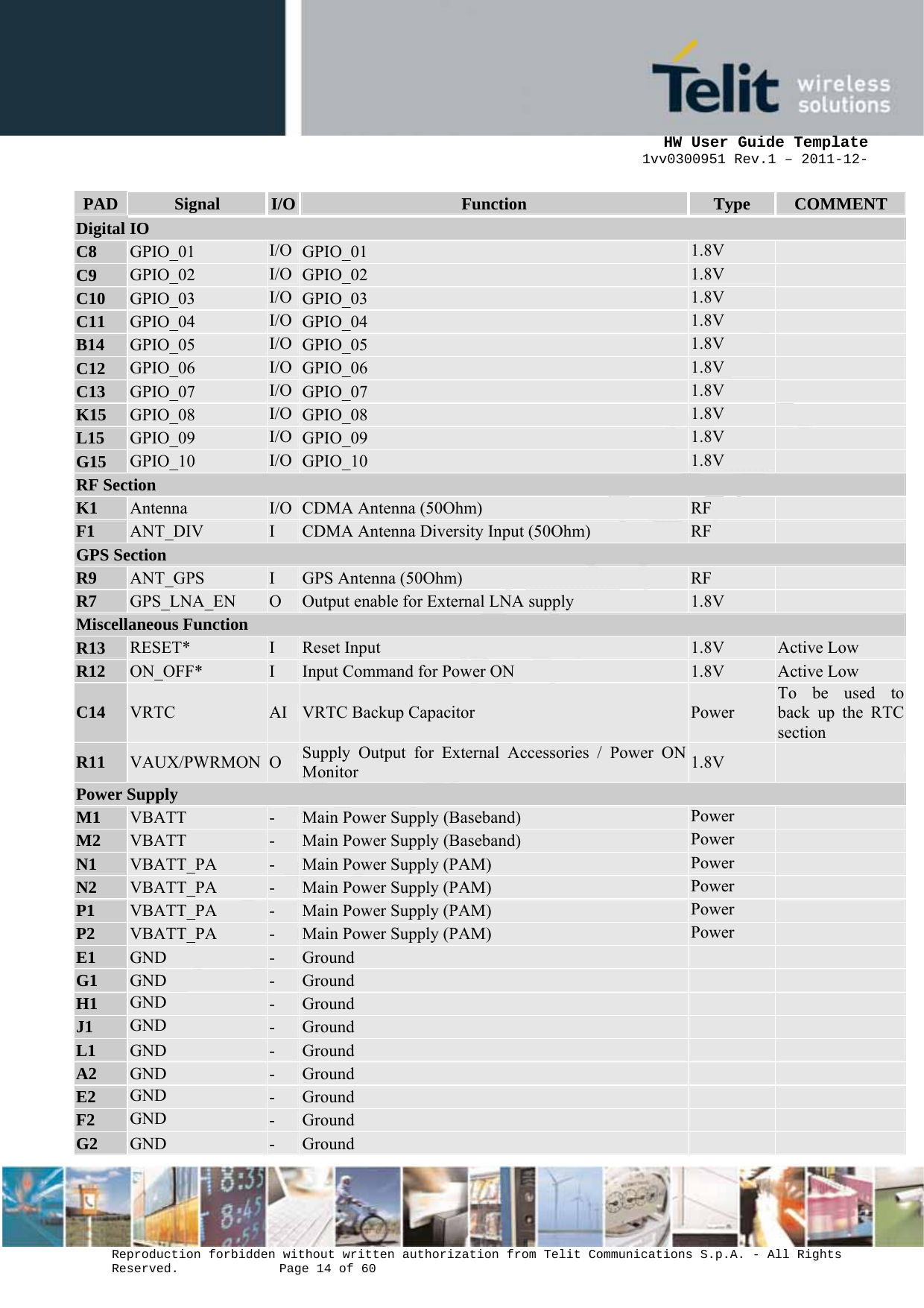
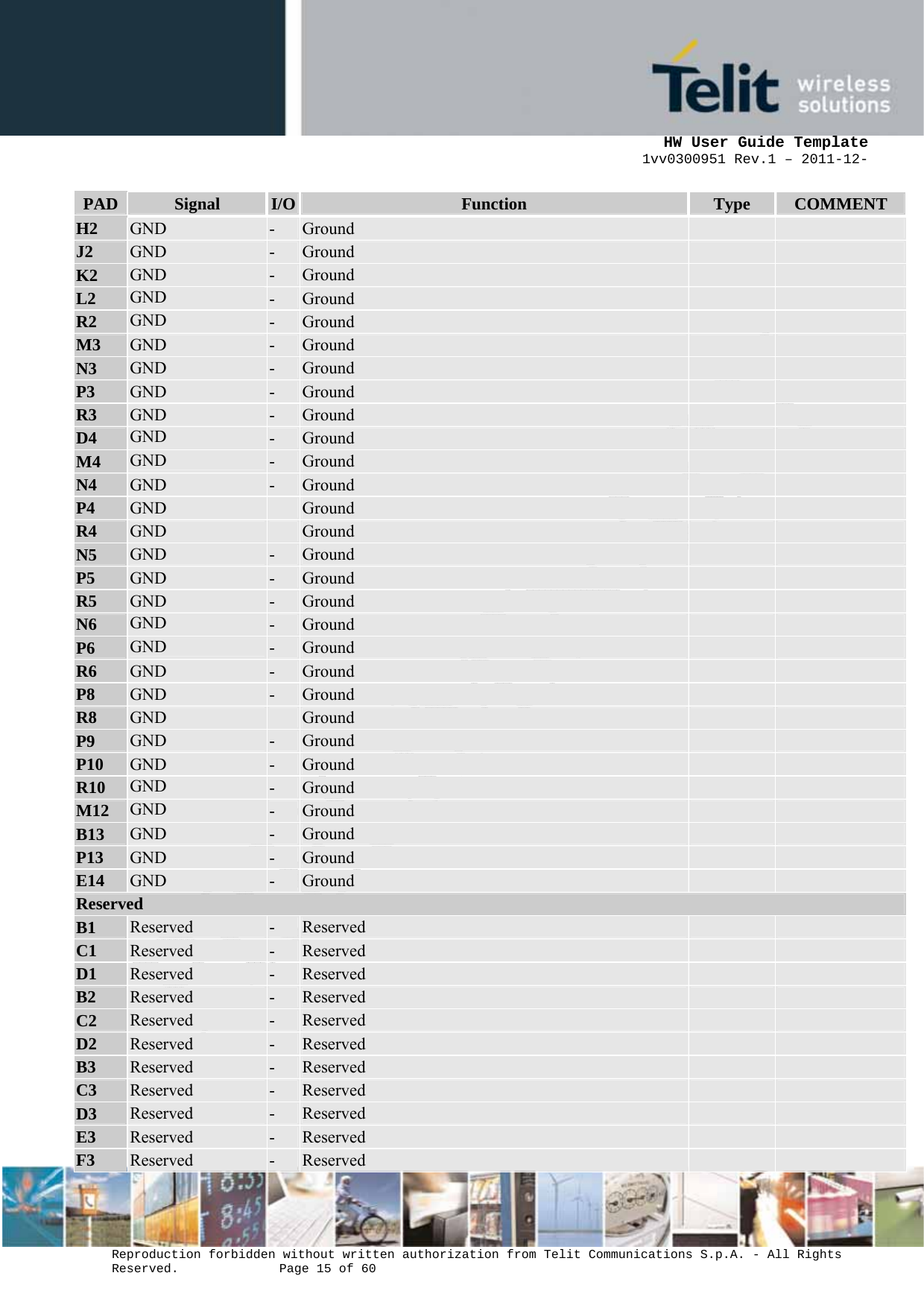
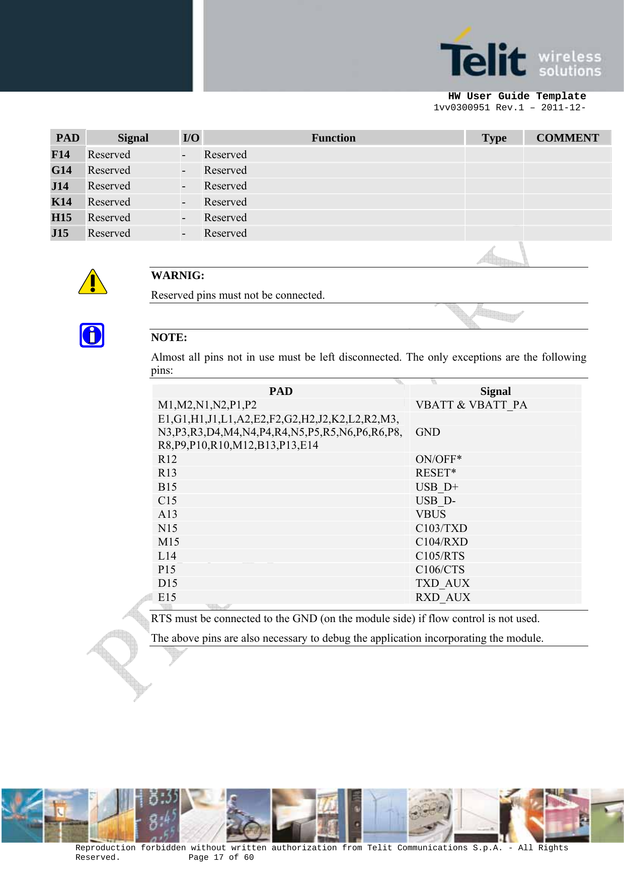
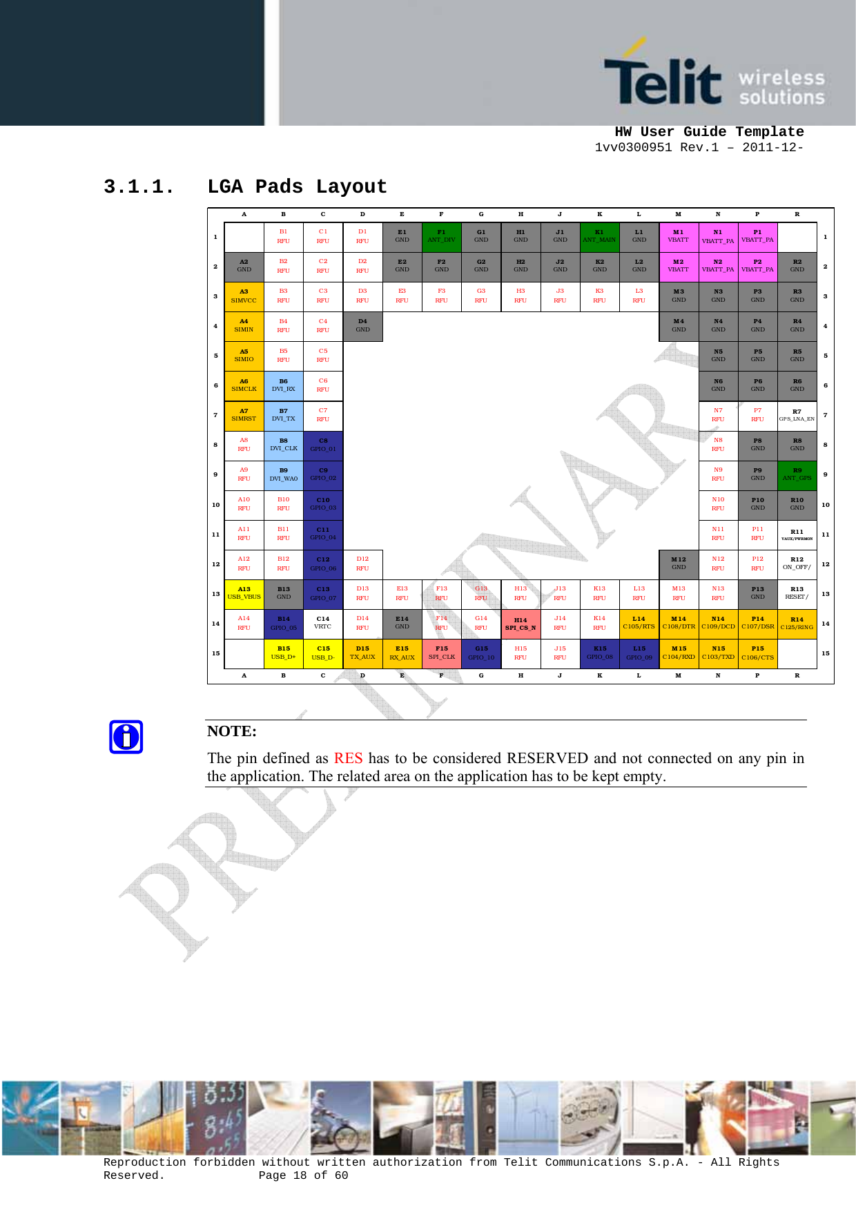
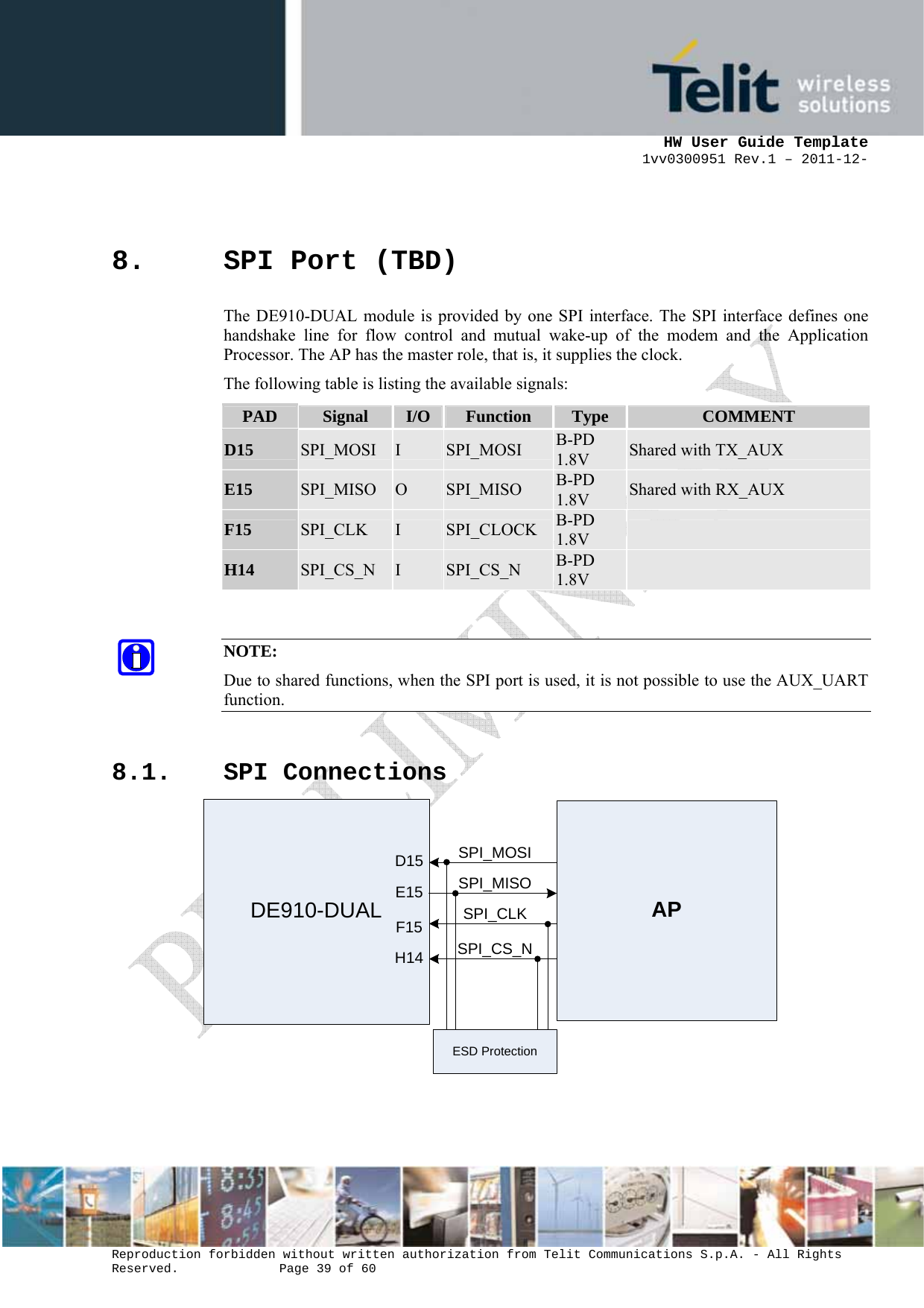
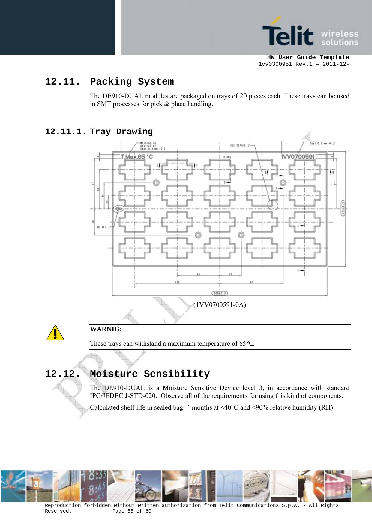
Telit Communications S p A DE910-DUAL DUAL BAND CDMA/GPS module User Manual
Telit Communications S.p.A. DUAL BAND CDMA/GPS module
UserManual.wiki
>
Telit Communications S p A
>
DE910-DUAL User Manual
>
user manual
Contents
1.
user manual
2.
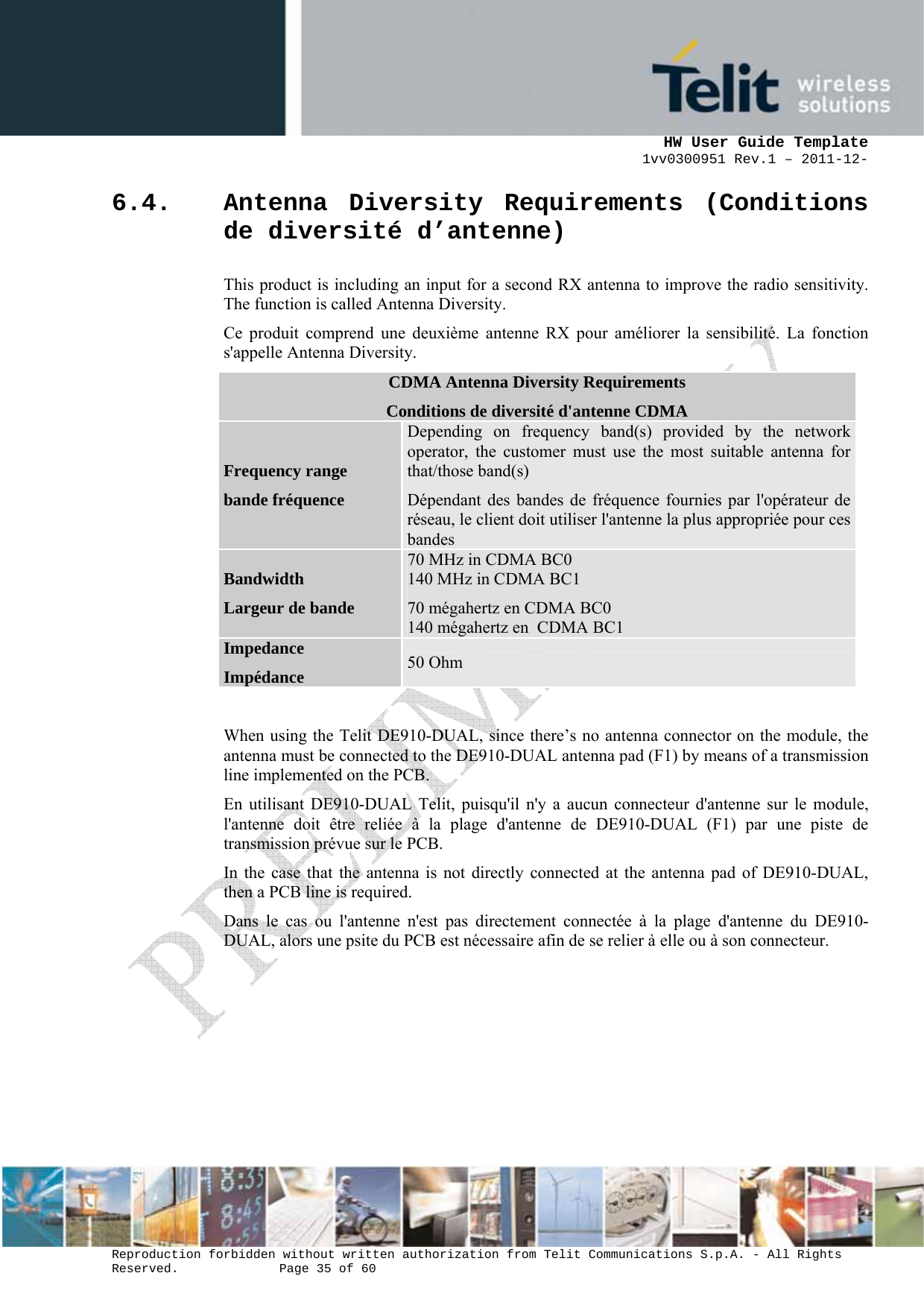
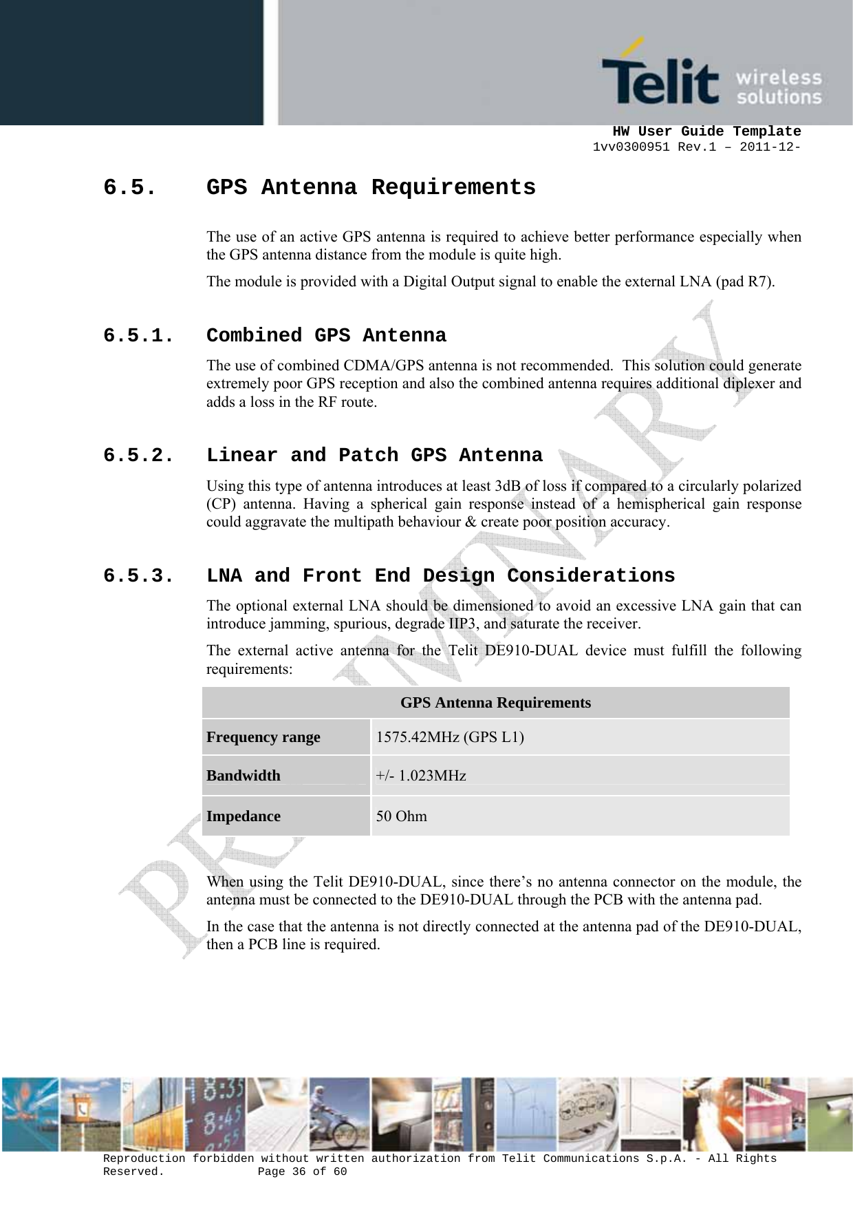
antenna information
3.
User Manual
user manual
Navigation menu
Upload a User Manual
Namespaces
Wiki Guide
HTML
PDF
Info
Views
User Manual
Discussion / Help
Navigation