Telit Communications S p A DE910-DUAL DUAL BAND CDMA/GPS module User Manual
Telit Communications S.p.A. DUAL BAND CDMA/GPS module
UserManual.wiki
>
Telit Communications S p A
>
DE910-DUAL User Manual
>
User Manual
Contents
1.
user manual
2.
antenna information
3.
User Manual
User Manual
Navigation menu
Upload a User Manual
Namespaces
Wiki Guide
HTML
PDF
Info
Views
User Manual
Discussion / Help
Navigation


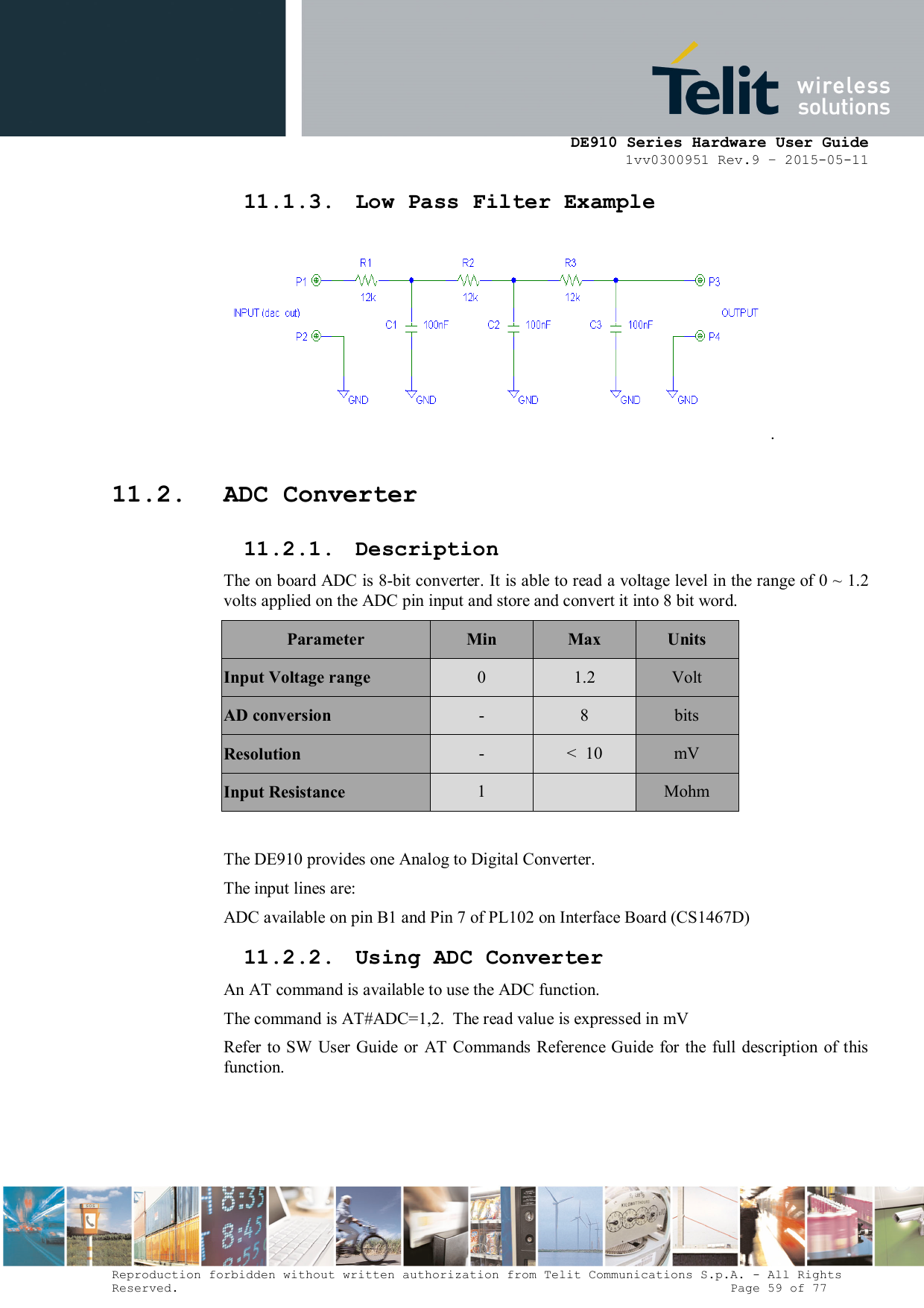
![DE910 Series Hardware User Guide 1vv0300951 Rev.9 – 2015-05-11 Reproduction forbidden without written authorization from Telit Communications S.p.A. - All Rights Reserved. Page 58 of 77 11. DAC and ADC section 11.1. DAC Converter 11.1.1. Description The DE910 module provides a Digital to Analog Converter. The signal (named DAC_OUT) is available on pin C13 of the DE910 module and on pin 6 of PL302 on Interface Board (CS1467D). The on board DAC is in the range from 0 to 1023. However, an external low-pass filter is necessary. Parameter Min Max Units Voltage range (filtered) 0 1.8 Volt Range 0 1023 Steps The precision is 1023 steps, so since the maximum voltage is 2V, the integrated voltage could be calculated with the following formula: Integrated output voltage = 2 * value / 1023 DAC_OUT line must be integrated (for example with a low band pass filter) in order to obtain an analog voltage. 11.1.2. Enabling DAC An AT command is available to use the DAC function. The command is: AT#DAC[=<enable>[,<value>]] <value> - scale factor of the integrated output voltage (0..1023 ~ 10 bit precision) it must be present if <enable>=1 Refer to SW User Guide or AT Commands Reference Guide for the full description of this function. NOTE: The DAC frequency is selected internally. D/A converter must not be used during POWERSAVING.](https://usermanual.wiki/Telit-Communications-S-p-A/DE910-DUAL.User-Manual/User-Guide-2614387-Page-58.png)