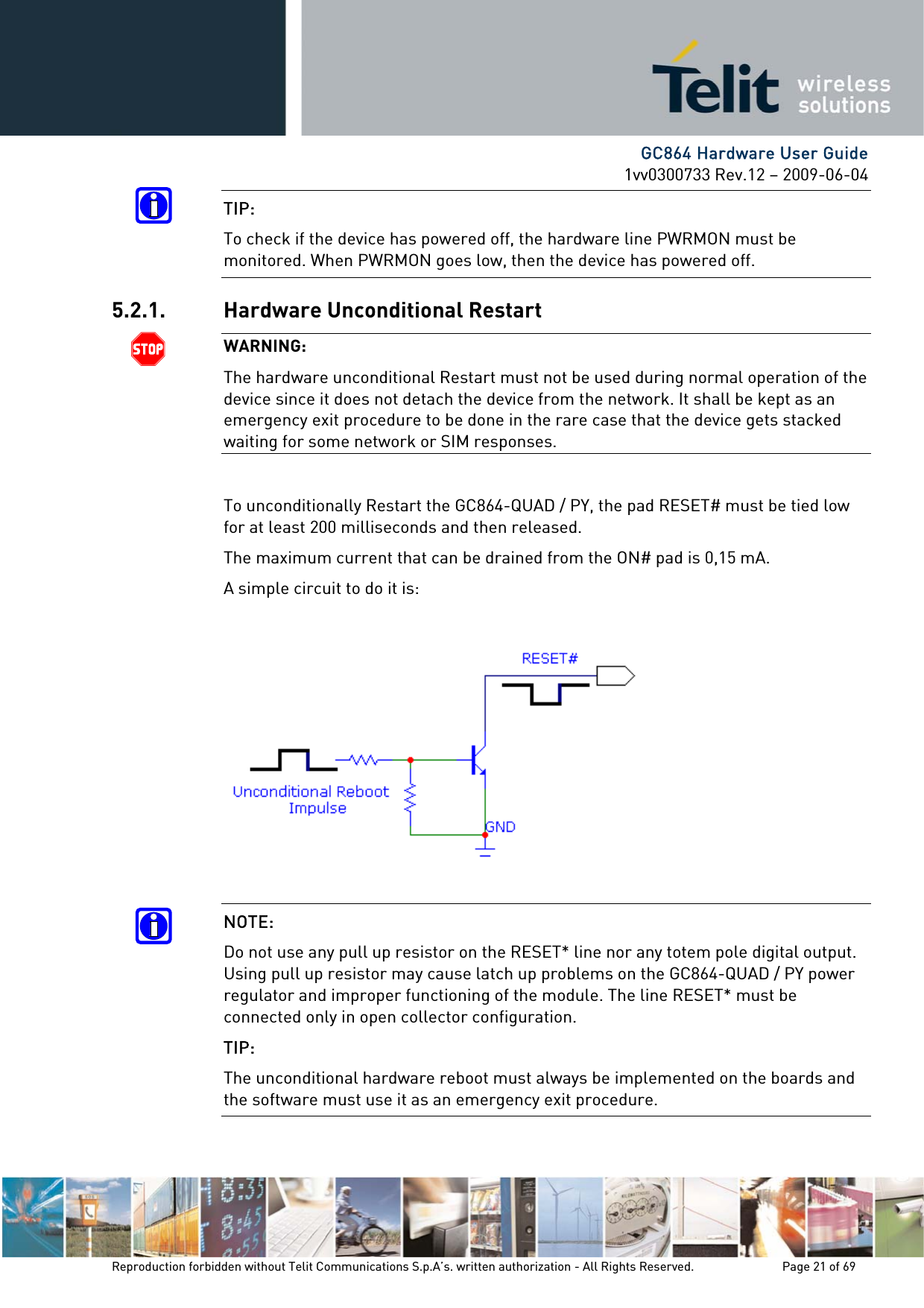
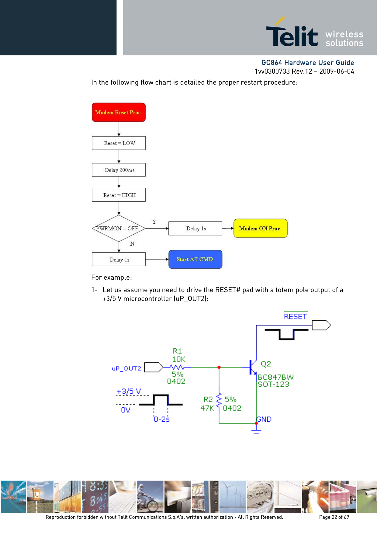
Telit Communications S p A GC864QC2 Quadband GSM/ GPRS Module User Manual GC864 Hardware User Guide
Telit Communications S.p.A. Quadband GSM/ GPRS Module GC864 Hardware User Guide
UserManual.wiki
>
Telit Communications S p A
>
GC864QC2 User Manual
User Manual
Navigation menu
Upload a User Manual
Namespaces
Wiki Guide
HTML
PDF
Info
Views
User Manual
Discussion / Help
Navigation


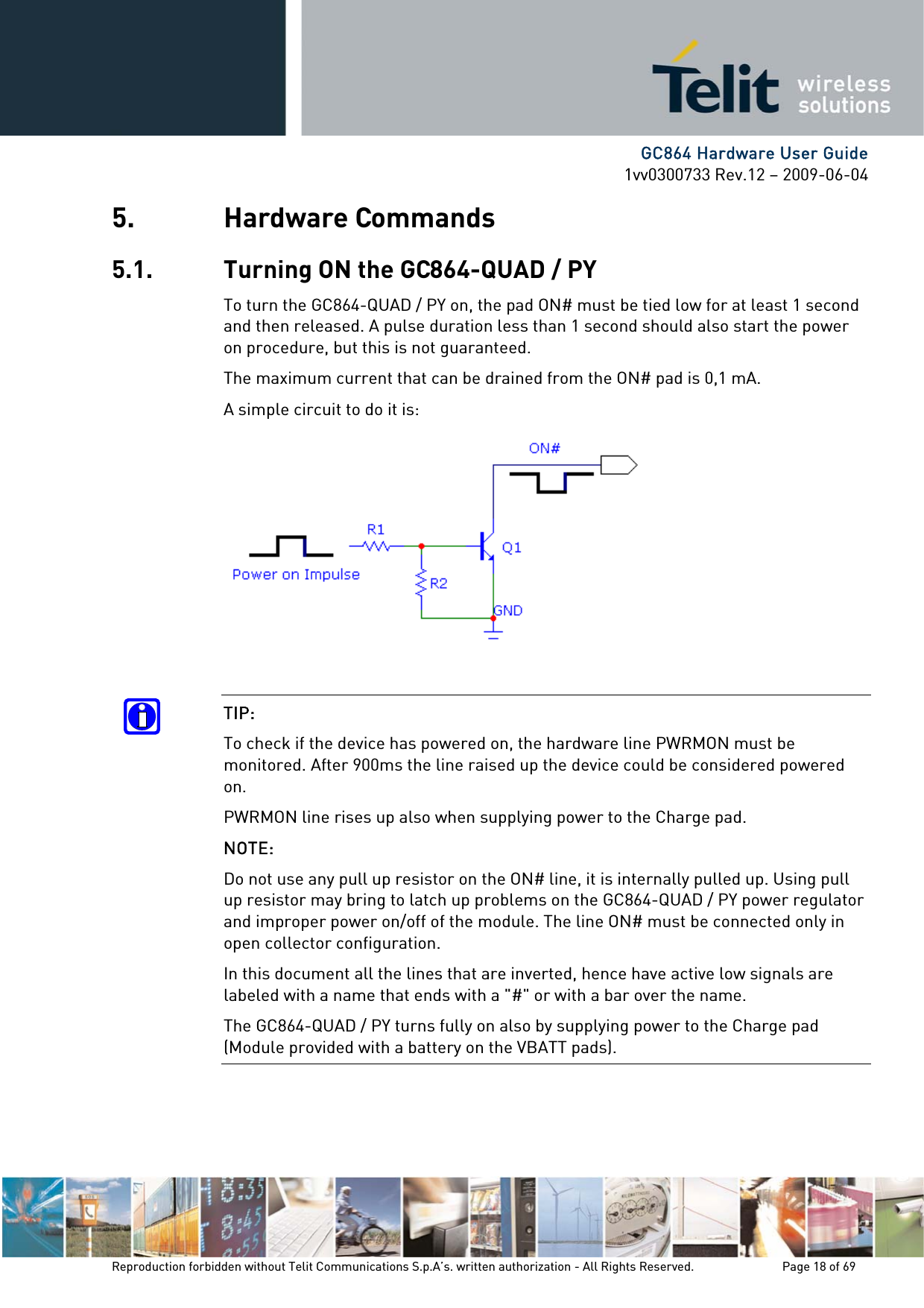


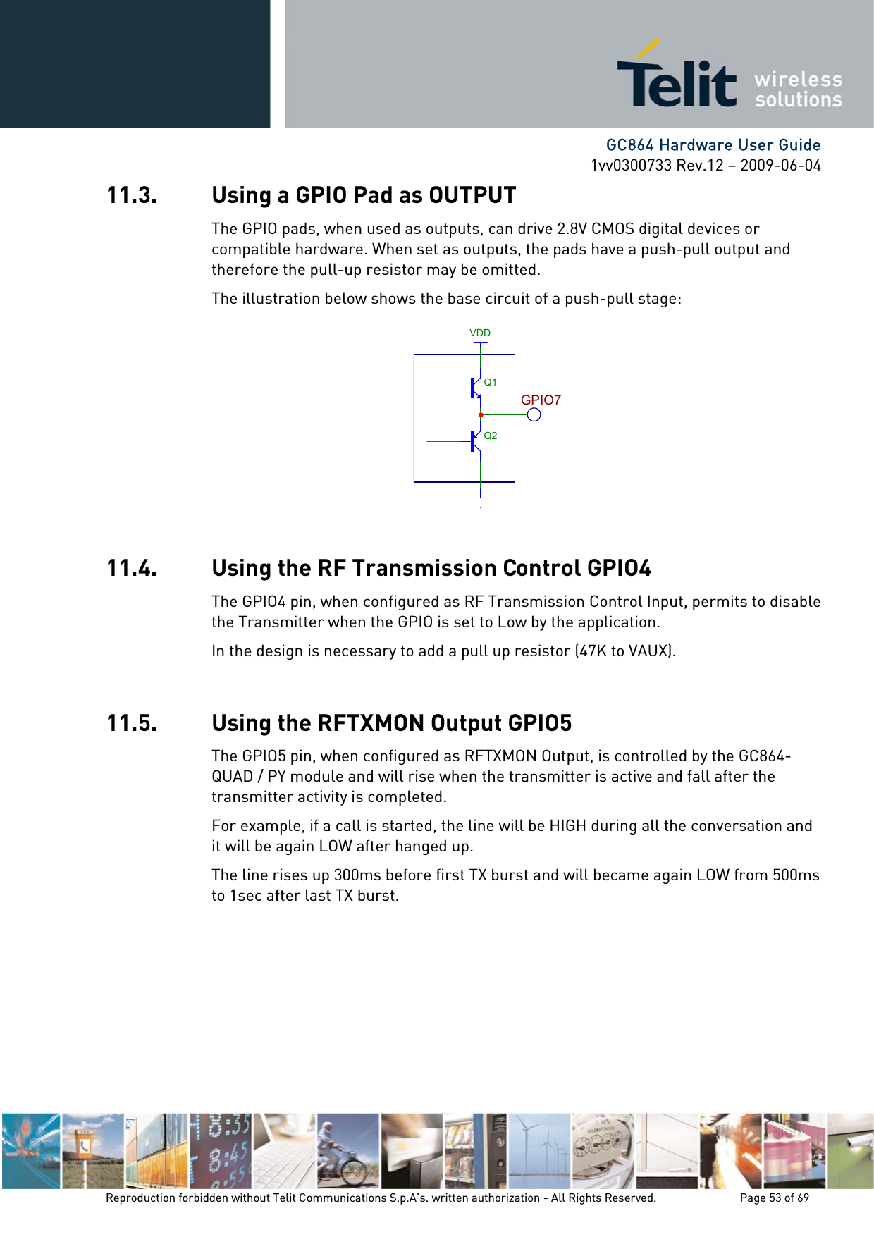
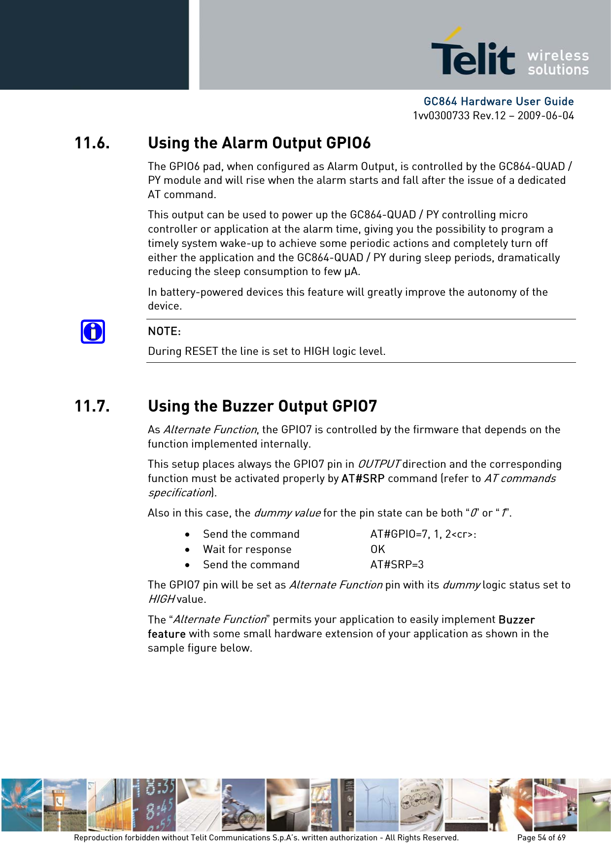
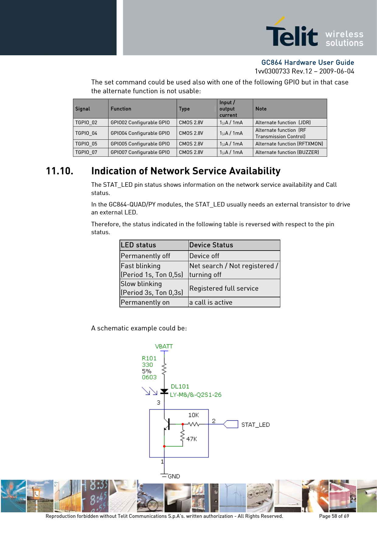
![GC864 Hardware User Guide 1vv0300733 Rev.12 – 2009-06-04 Not all GPIO pads support all these three modes: • GPIO2 supports all three modes and can be input, output, Jamming Detect Output (Alternate function) • GPIO4 supports all three modes and can be input, output, RF Transmission Control (Alternate function) • GPIO5 supports all three modes and can be input, output, RFTX monitor output (Alternate function) • GPIO6 supports all three modes and can be input, output, alarm output (Alternate function) • GPIO7 supports all three modes and can be input, output, buzzer output (Alternate function) ch1: ON_OFF (2sec) ch2: GPIO 06 [ bis ] GC864 Reproduction forbidden without Telit Communications S.p.A’s. written authorization - All Rights Reserved. Page 51 of 69](https://usermanual.wiki/Telit-Communications-S-p-A/GC864QC2/User-Guide-1303214-Page-51.png)

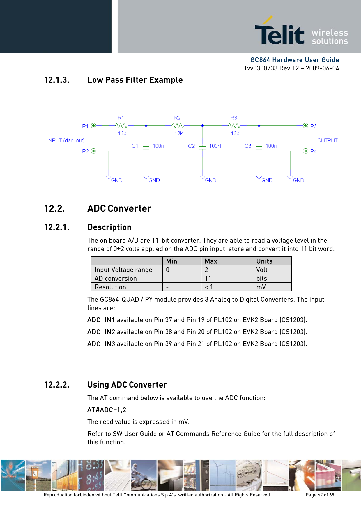
![GC864 Hardware User Guide 1vv0300733 Rev.12 – 2009-06-04 12. DAC and ADC Section 12.1. DAC Converter 12.1.1. Description The GC864-QUAD / PY module provides a Digital to Analog Converter. The signal (named DAC_OUT) is available on pin 40 of the GC864-QUAD / PY module and on pin 17 of PL102 on EVK2 Board (CS1203). The on board DAC is a 10-bit converter, able to generate a analogue value based a specific input in the range from 0 up to 1023. However, an external low-pass filter is necessary. Min Max Units Voltage range (filtered) 0 2,6 Volt Range 0 1023 Steps The precision is 10 bits, so if we consider that the maximum voltage is 2V, the integrated voltage could be calculated with the following formula: Integrated output voltage = 2 * value / 1023 DAC_OUT line must be integrated (for example with a low band pass filter) in order to obtain an analog voltage. 12.1.2. Enabling DAC The AT command below is available to use the DAC function: AT#DAC[=<enable>[,<value>]] <value> – scale factor of the integrated output voltage (0–1023, with 10 bit precision), and it must be present if <enable>=1. Refer to SW User Guide or AT Commands Reference Guide for the full description of this function. Refer to SW User Guide or AT Commands Reference Guide for the full description of this function. NOTE: The DAC frequency is selected internally. D/A converter must not be used during POWERSAVING. Reproduction forbidden without Telit Communications S.p.A’s. written authorization - All Rights Reserved. Page 61 of 69](https://usermanual.wiki/Telit-Communications-S-p-A/GC864QC2/User-Guide-1303214-Page-61.png)