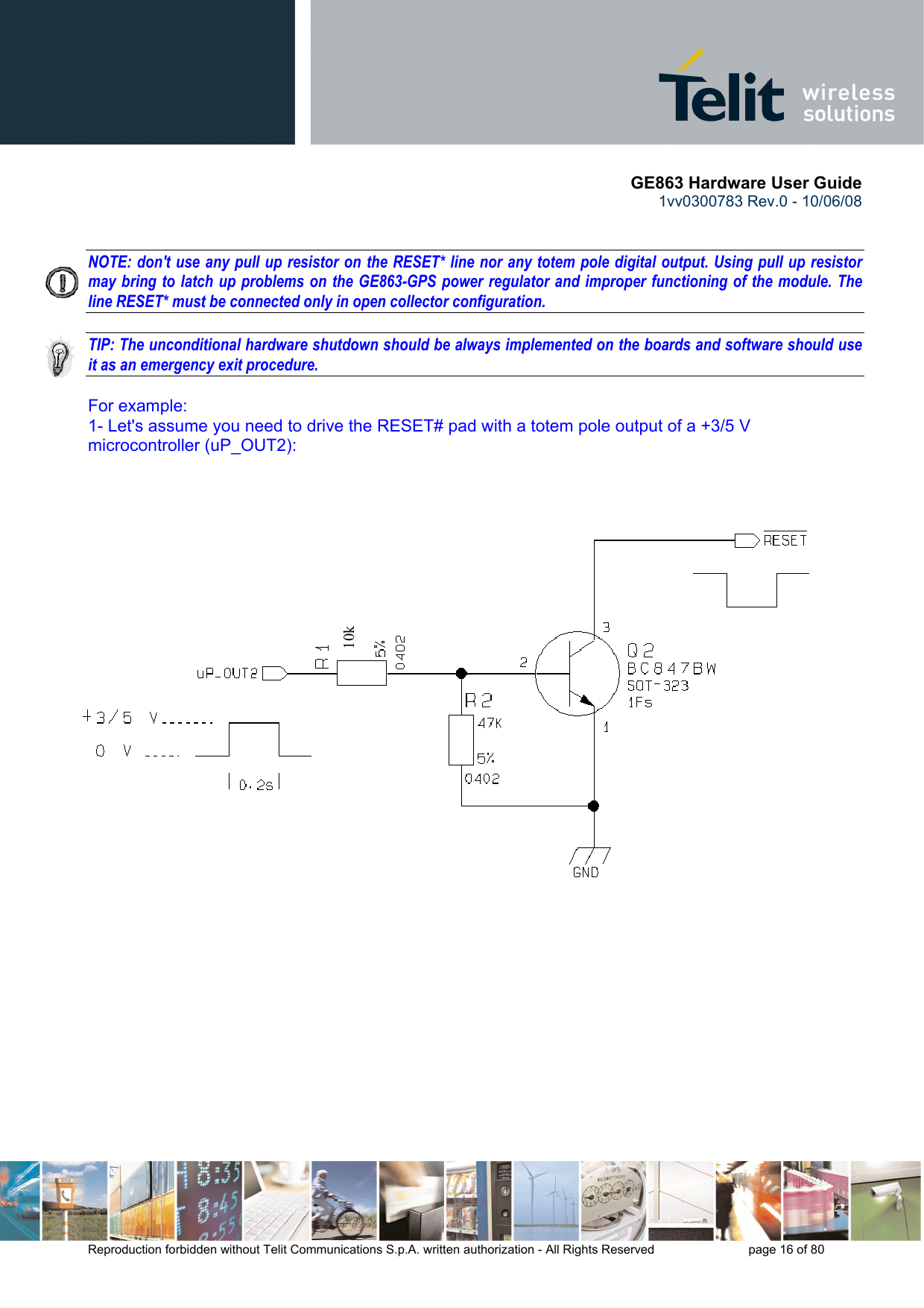
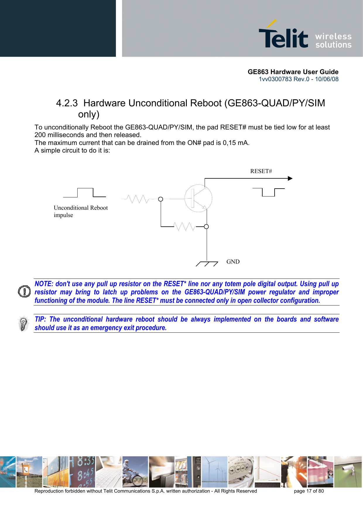
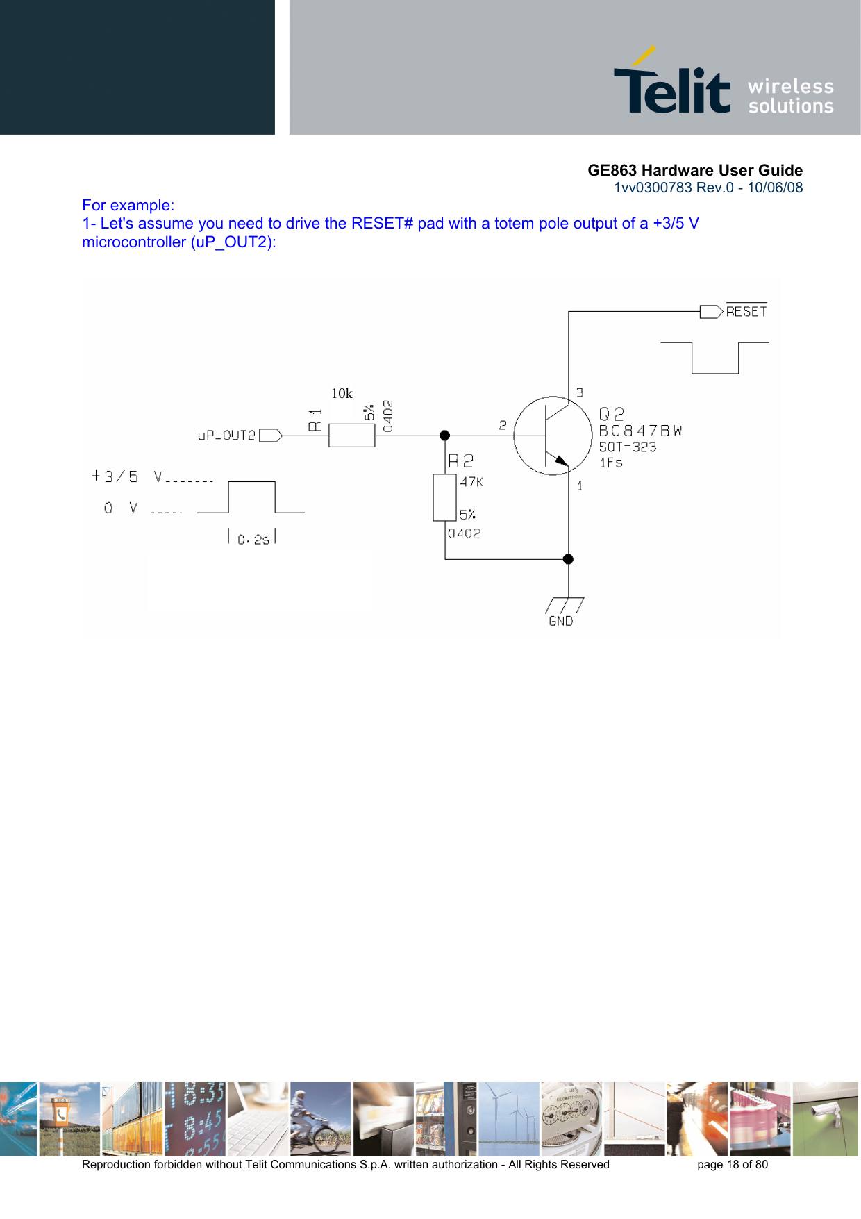
Telit Communications S p A GE863S Quad-Band GSM/GPRS module User Manual GE863 GPS Harware User Guide
Telit Communications S.p.A. Quad-Band GSM/GPRS module GE863 GPS Harware User Guide
UserManual.wiki
>
Telit Communications S p A
>
GE863S User Manual
Manual
Navigation menu
Upload a User Manual
Namespaces
Wiki Guide
HTML
PDF
Info
Views
User Manual
Discussion / Help
Navigation

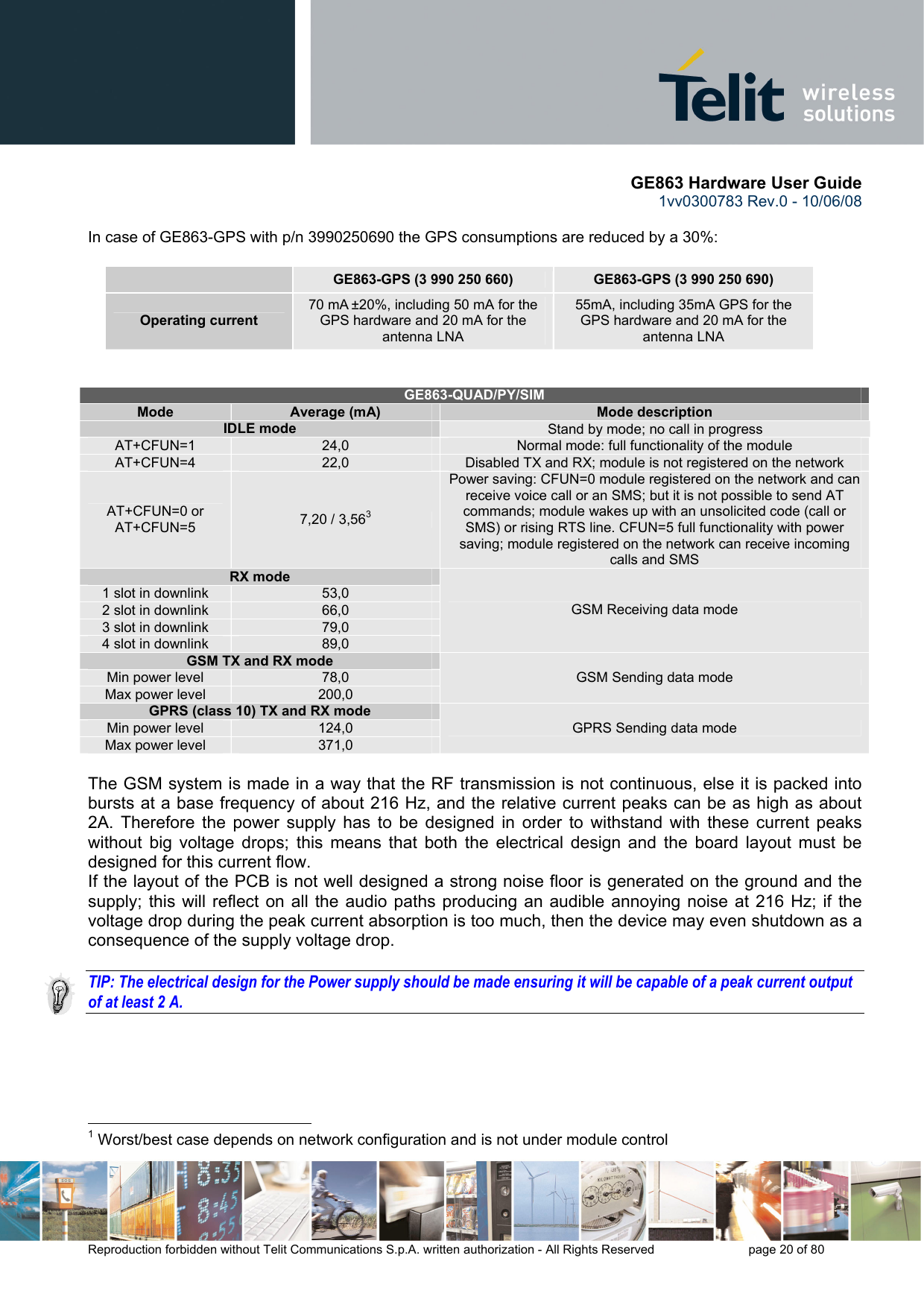
![GE863 Hardware User Guide 1vv0300783 Rev.0 - 10/06/08 Reproduction forbidden without Telit Communications S.p.A. written authorization - All Rights Reserved page 19 of 80 4.3 Power Supply The power supply circuitry and board layout are a very important part in the full product design and they strongly reflect on the product overall performances, hence read carefully the requirements and the guidelines that will follow for a proper design. 4.4 Power Supply Requirements POWER SUPPLY Nominal Supply Voltage 3.8 V Max Supply Voltage 4.2 V Supply voltage range 3.4 V - 4.2 V GE863-GPS Mode Average [mA] Mode description IDLE mode with GPS OFF Stand by mode; no call in progress; GPS OFF AT+CFUN=1 24,0 Normal mode: full functionality of the module AT+CFUN=4 22,0 Disabled TX and RX; module is not registered on the network AT+CFUN=0 or AT+CFUN=5 7,3 / 3,41 Power saving: CFUN=0 module registered on the network and can receive voice call or an SMS; but it is not possible to send AT commands; module wakes up with an unsolicited code (call or SMS) or rising RTS line. CFUN=5 full functionality with power saving; module registered on the network can receive incoming calls and SMS IDLE mode with GPS ON2 full power mode AT+CFUN=1 113,0 AT+CFUN=4 111,0 Stand by mode; no call in progress; GPS ON IDLE mode with GPS ON trickle power mode AT+CFUN=1 64,0 AT+CFUN=4 62,0 Stand by mode; no call in progress; GPS consumption reduced maintaining the NMEA sentences IDLE mode with GPS ON push to fix mode AT+CFUN=1 24,0 AT+CFUN=4 22,0 AT+CFUN=5 10,0 Stand by mode; no call in progress; GPS performs a fix and then it switches off for the defined period RX mode 1 slot in downlink 53,0 2 slot in downlink 65,0 3 slot in downlink 78,0 4 slot in downlink 91,0 GSM Receiving data mode GSM TX and RX mode GPS ON Min power level 135,0 Max power level 254,0 GSM Sending data mode GPRS (class 10) TX and RX mode GPS ON Min power level 187,0 Max power level 430,0 GPRS Sending data mode 1 Worst/best case depends on network configuration and is not under module control 2 The values reported are with GPS antenna current consumption (22mA) included](https://usermanual.wiki/Telit-Communications-S-p-A/GE863S/User-Guide-1038627-Page-19.png)

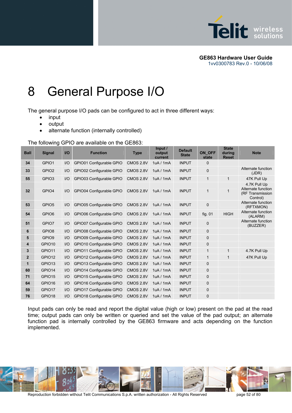
![GE863 Hardware User Guide 1vv0300783 Rev.0 - 10/06/08 Reproduction forbidden without Telit Communications S.p.A. written authorization - All Rights Reserved page 53 of 80 Not all GPIO pads support all these three modes: • GPIO1, GPIO3, GPIO8 to GPIO18 support both input and output mode but not Alternate function. • GPIO2 supports all three modes and can be input, output, Jamming Detect Output (Alternate function) • GPIO4 supports all three modes and can be input, output, RF Transmission Control (Alternate function) • GPIO5 supports all three modes and can be input, output, RFTX monitor output (Alternate function) • GPIO6 supports all three modes and can be input, output, alarm output (Alternate function) • GPIO7 supports all three modes and can be input, output, buzzer output (Alternate function) All GPIO pads are 2.8V CMOS signals and their interface levels are the same specified in the paragraph 5. fig. 01 ch1: ON_OFF (2sec) ch2: GPIO 06 [ bis ] GE863-GPS](https://usermanual.wiki/Telit-Communications-S-p-A/GE863S/User-Guide-1038627-Page-53.png)

![GE863 Hardware User Guide 1vv0300783 Rev.0 - 10/06/08 Reproduction forbidden without Telit Communications S.p.A. written authorization - All Rights Reserved page 65 of 80 11.1.2 Enabling DAC An AT command is available to use the DAC function. The command is AT#DAC[=<enable>[,<value>]] <value> - scale factor of the integrated output voltage (0..1023 - 10 bit precision) it must be present if <enable>=1 Refer to SW User Guide or to AT Commands Reference Guide for the full description of this function. NOTE: The DAC frequency is selected internally. D/A converter must not be used during POWERSAVING. 11.1.3 Low Pass Filter Example](https://usermanual.wiki/Telit-Communications-S-p-A/GE863S/User-Guide-1038627-Page-65.png)
![GE863 Hardware User Guide 1vv0300783 Rev.0 - 10/06/08 Reproduction forbidden without Telit Communications S.p.A. written authorization - All Rights Reserved page 71 of 80 12.1.4 PCB pad Design “Non solder mask defined” (NSMD) type is recommended for the solder pads on the PCB. Recommendations for PCB pad dimensions Ball pitch [mm] 2 Solder resist opening diameter A [mm] 1,150 Metal pad diameter B [mm] 1 ± 0.05](https://usermanual.wiki/Telit-Communications-S-p-A/GE863S/User-Guide-1038627-Page-71.png)
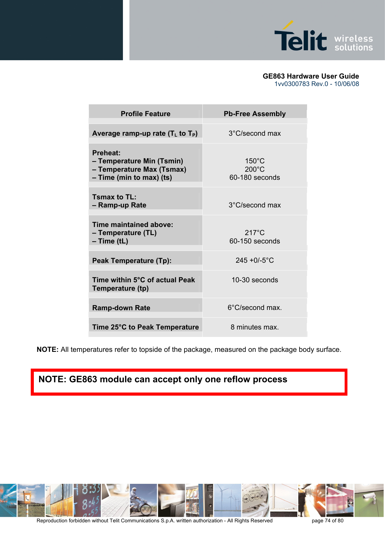
![GE863 Hardware User Guide 1vv0300783 Rev.0 - 10/06/08 Reproduction forbidden without Telit Communications S.p.A. written authorization - All Rights Reserved page 73 of 80 Recommendations for PCB pad surfaces: Finish Layer thickness [µm] Properties Electro-less Ni / Immersion Au 3 –7 / 0.05 – 0.15 Good solder ability protection, high shear force values The PCB must be able to resist the higher temperatures, which are occurring at the lead-free process. This issue should be discussed with the PCB-supplier. Generally, the wet-ability of tin-lead solder paste on the described surface plating is better compared to lead-free solder paste. 12.1.5 Solder paste Lead free Solder paste Sn/Ag/Cu 12.1.6 GE863 Solder Reflow The following is the recommended solder reflow profile](https://usermanual.wiki/Telit-Communications-S-p-A/GE863S/User-Guide-1038627-Page-73.png)