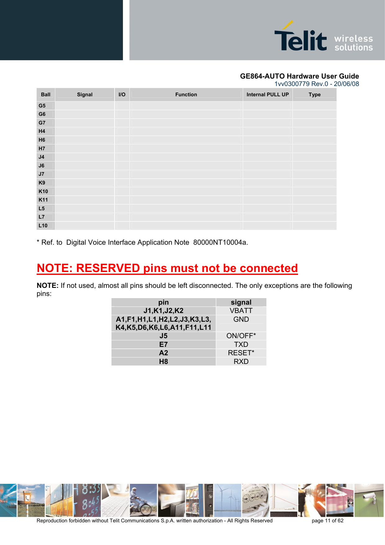
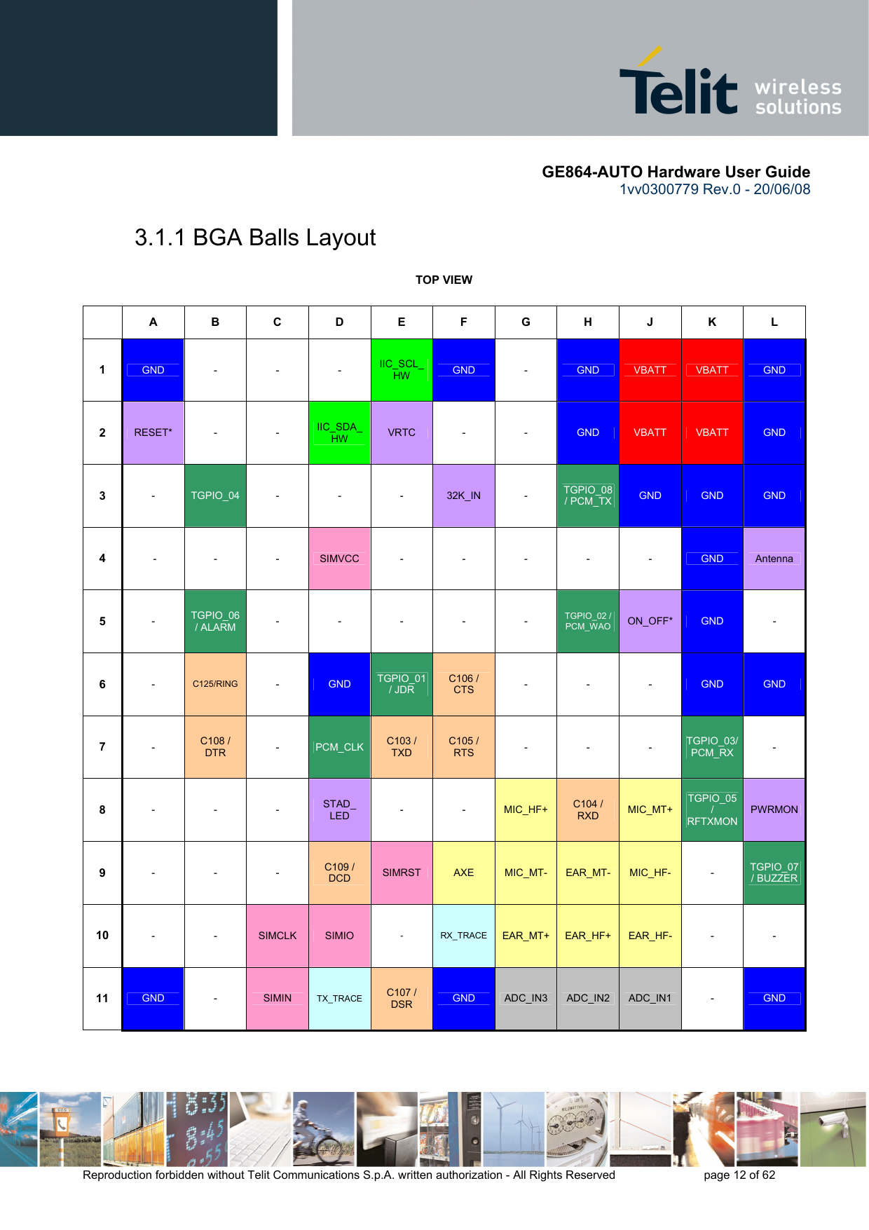
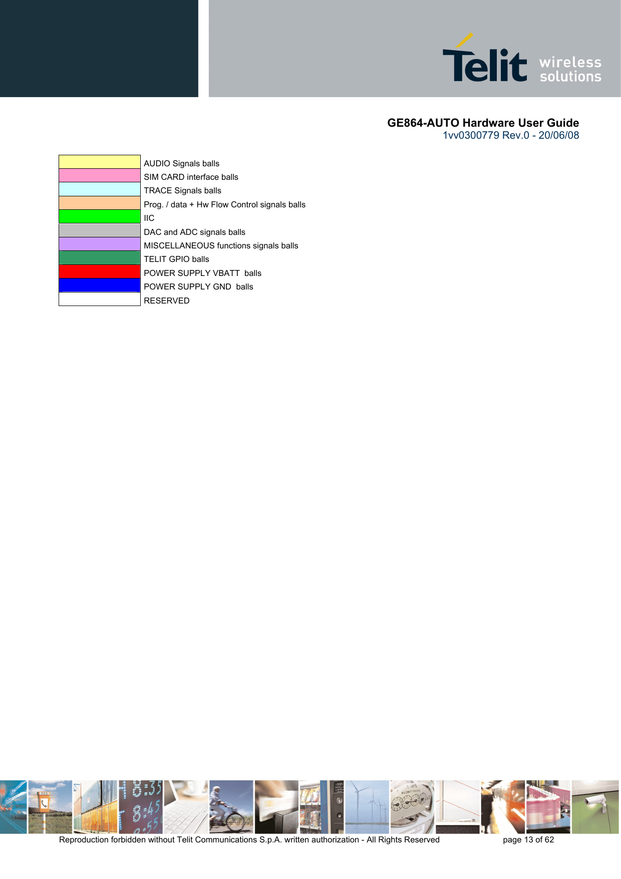
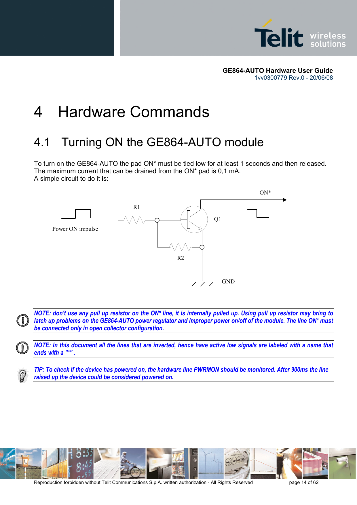
Telit Communications S p A GE864QA Quad-band GPRS Cell Module / GE864-QUAD Automotive User Manual GE864 Harware User Guide
Telit Communications S.p.A. Quad-band GPRS Cell Module / GE864-QUAD Automotive GE864 Harware User Guide
UserManual.wiki
>
Telit Communications S p A
>
GE864QA User Manual
User manual
Navigation menu
Upload a User Manual
Namespaces
Wiki Guide
HTML
PDF
Info
Views
User Manual
Discussion / Help
Navigation
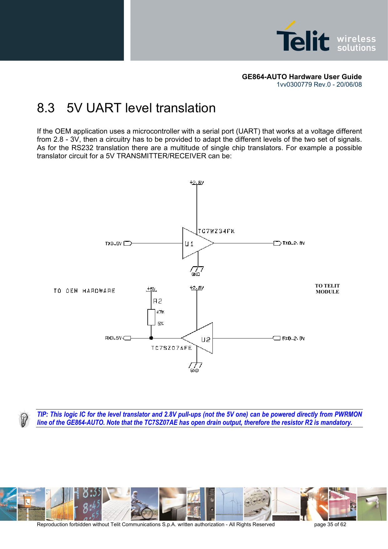
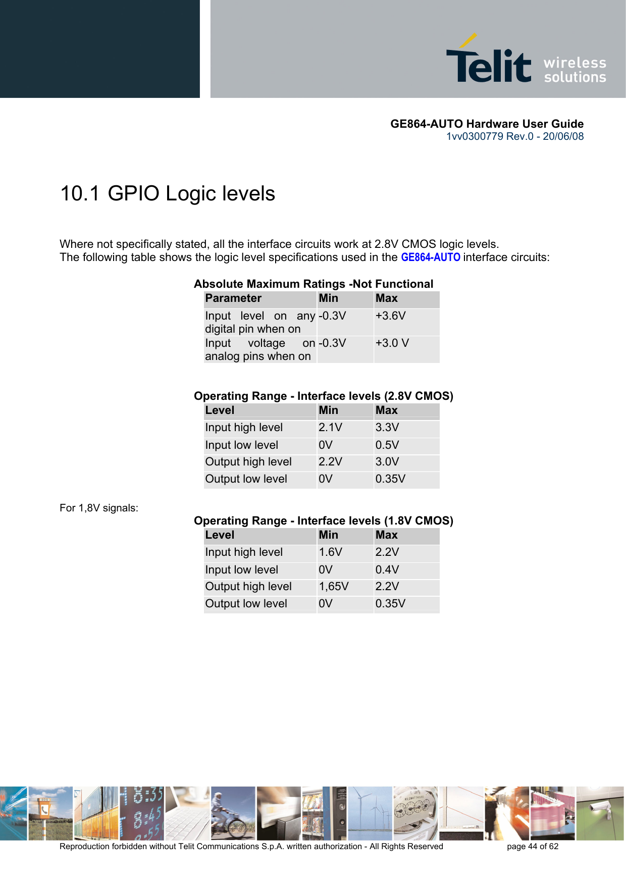
![GE864-AUTO Hardware User Guide 1vv0300779 Rev.0 - 20/06/08 Reproduction forbidden without Telit Communications S.p.A. written authorization - All Rights Reserved page 43 of 62 Fig.01ch1: ON_OFF (2sec) ch2: GPIO 06 [ bis ] GE864-AUTO](https://usermanual.wiki/Telit-Communications-S-p-A/GE864QA/User-Guide-1068129-Page-43.png)
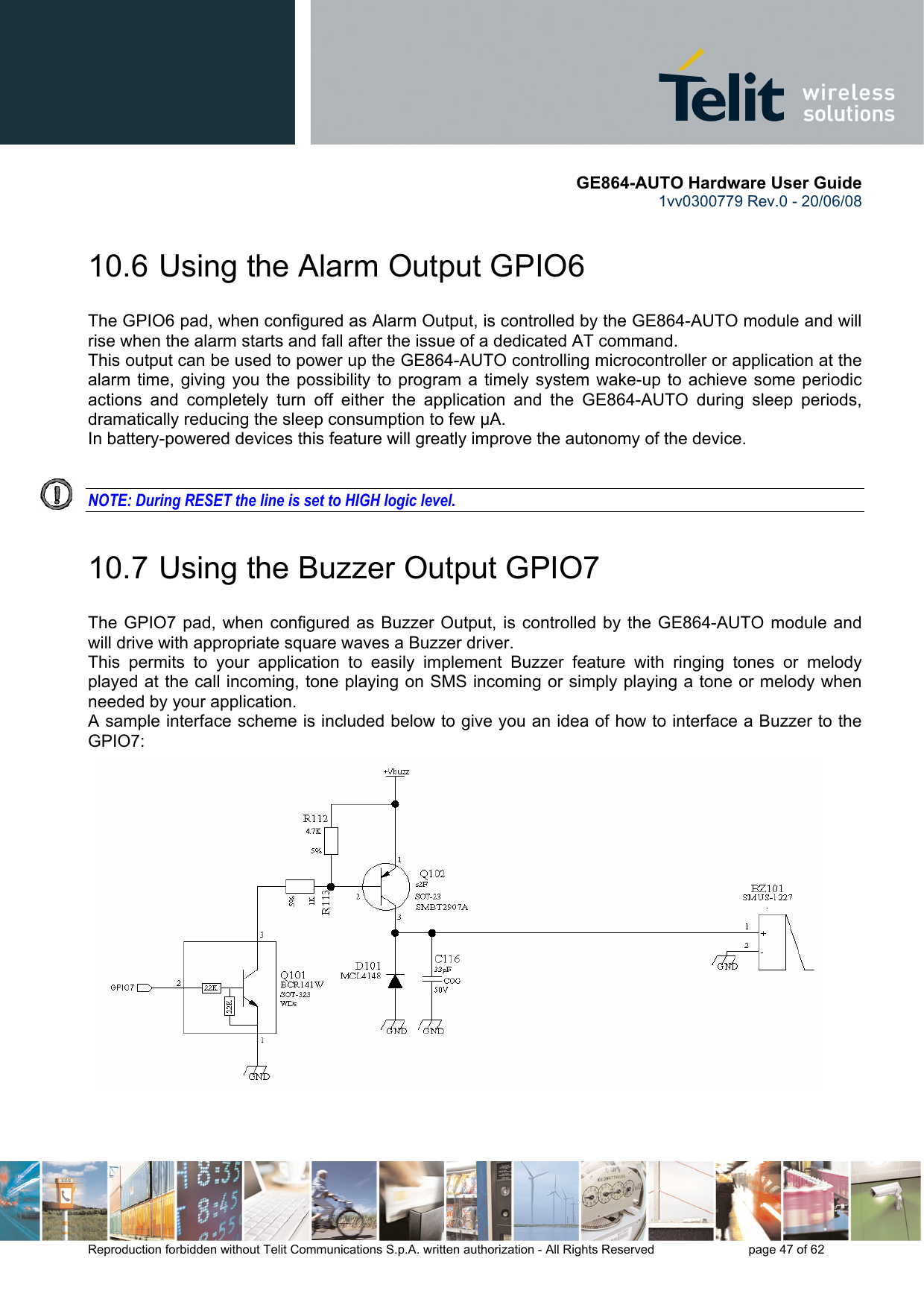
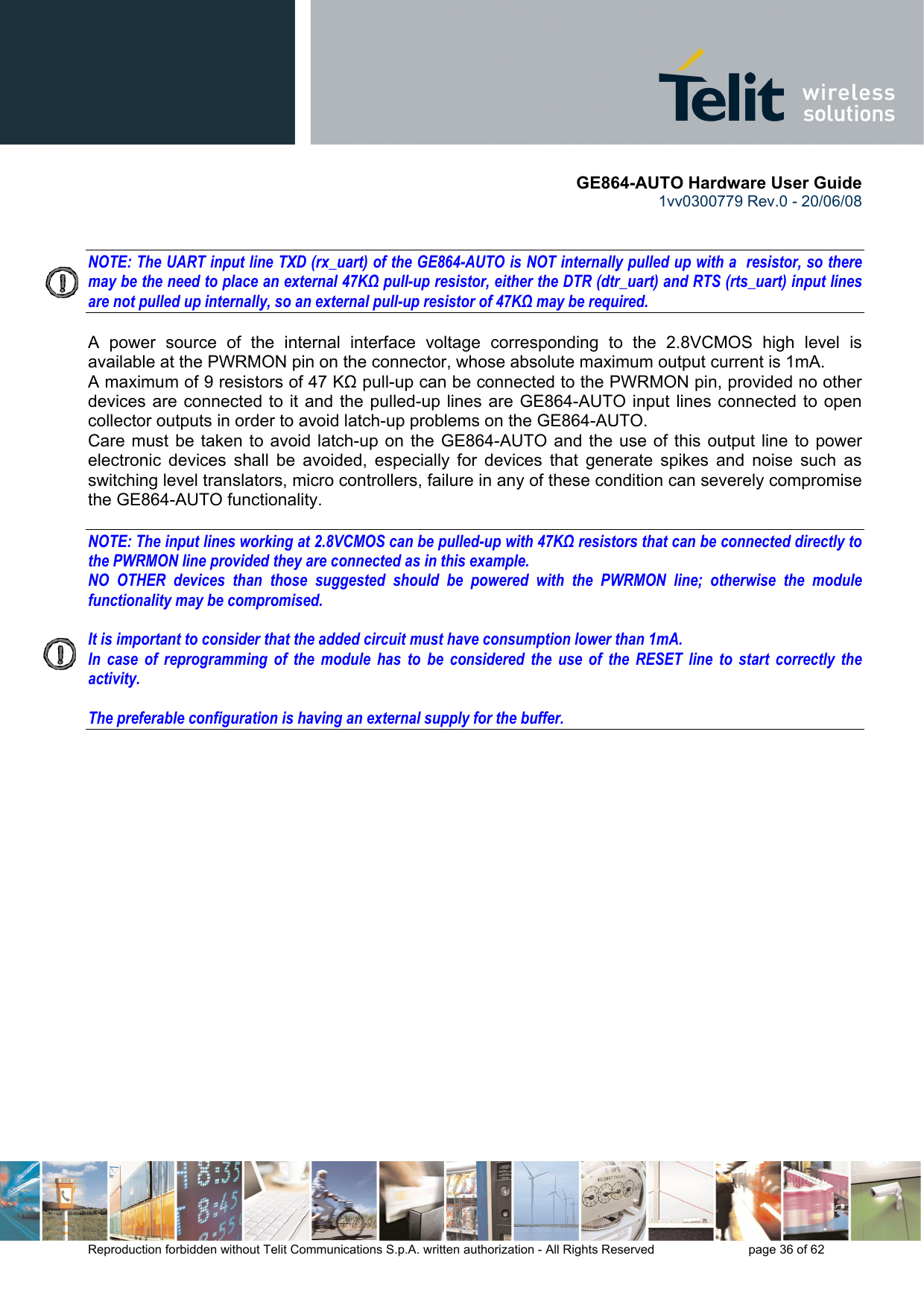
![GE864-AUTO Hardware User Guide 1vv0300779 Rev.0 - 20/06/08 Reproduction forbidden without Telit Communications S.p.A. written authorization - All Rights Reserved page 55 of 62 11.2.6 PCB pad design Non solder mask defined” (NSMD) type is recommended for the solder pads on the PCB. Recommendations for PCB pad dimensions Ball pitch [mm] 2,5 Solder resist opening diameter A [mm] 1,150 Metal pad diameter B [mm] 1 ± 0.05 Placement of microvias not covered by solder resist is not recommended inside the “Solder resist opening”, unless the microvia carry the same signal of the pad itself.](https://usermanual.wiki/Telit-Communications-S-p-A/GE864QA/User-Guide-1068129-Page-55.png)
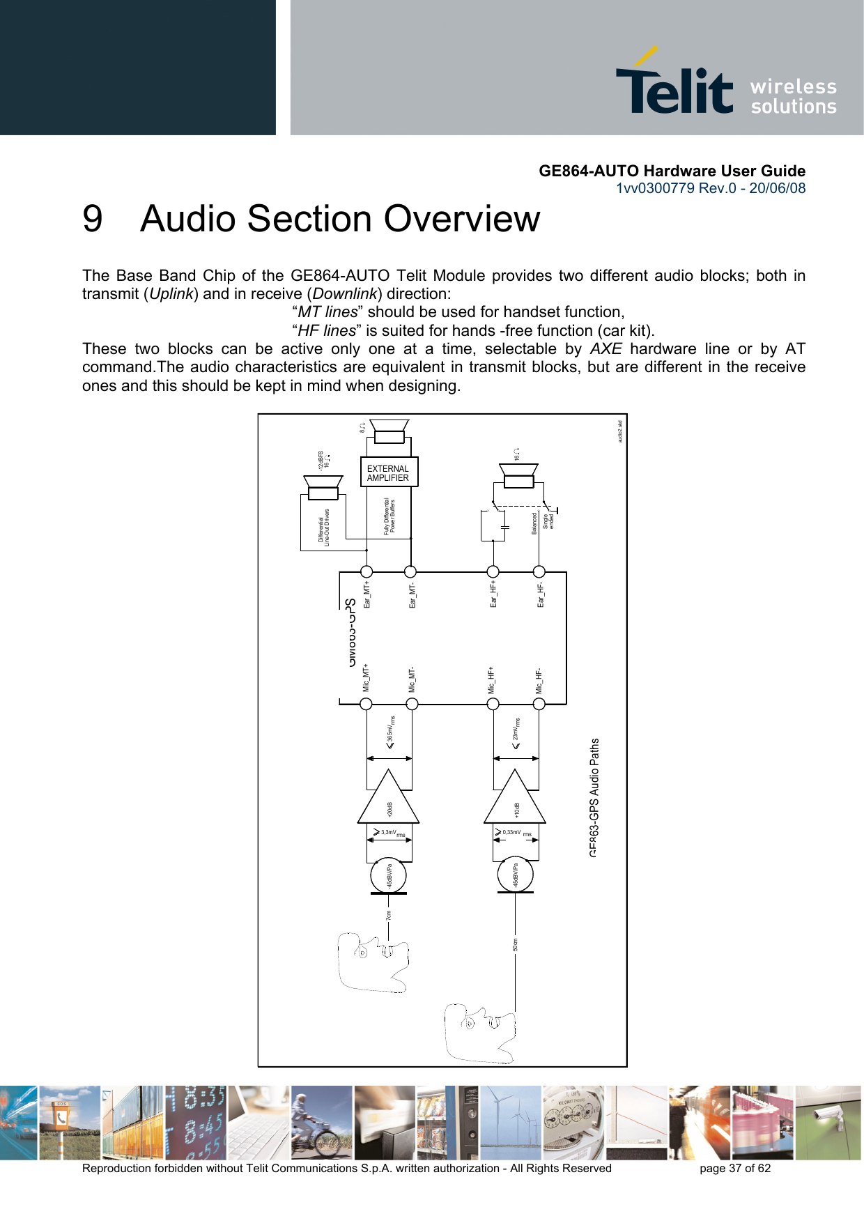
![GE864-AUTO Hardware User Guide 1vv0300779 Rev.0 - 20/06/08 Reproduction forbidden without Telit Communications S.p.A. written authorization - All Rights Reserved page 56 of 62 Holes in pad are allowed only for blind holes and not for through holes. Recommendations for PCB pad surfaces: Finish Layer thickness [µm] Properties Electro-less Ni / Immersion Au 3 –7 / 0.05 – 0.15 good solder ability protection, high shear force values The PCB must be able to resist the higher temperatures which are occurring at the lead-free process. This issue should be discussed with the PCB-supplier. Generally, the wettability of tin-lead solder paste on the described surface plating is better compared to lead-free solder paste. 11.2.7 Solder paste Lead free Solder paste Sn/Ag/Cu](https://usermanual.wiki/Telit-Communications-S-p-A/GE864QA/User-Guide-1068129-Page-56.png)