Telit Communications S p A GE864QC2 Quadband GSM/ GPRS Module User Manual GE864 QUAD Hardware User Guide
Telit Communications S.p.A. Quadband GSM/ GPRS Module GE864 QUAD Hardware User Guide
UserManual.wiki
>
Telit Communications S p A
>
GE864QC2 User Manual
User Manual
Navigation menu
Upload a User Manual
Namespaces
Wiki Guide
HTML
PDF
Info
Views
User Manual
Discussion / Help
Navigation


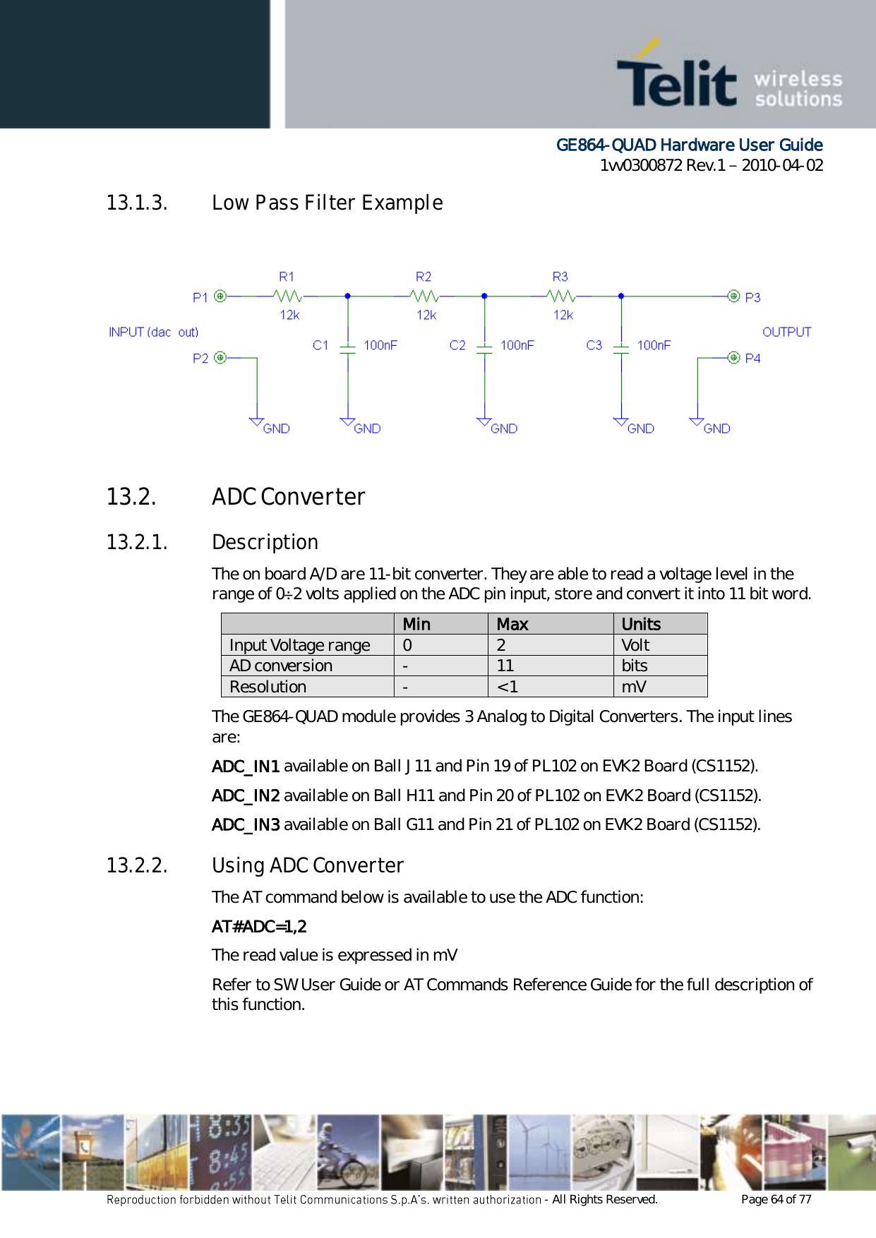
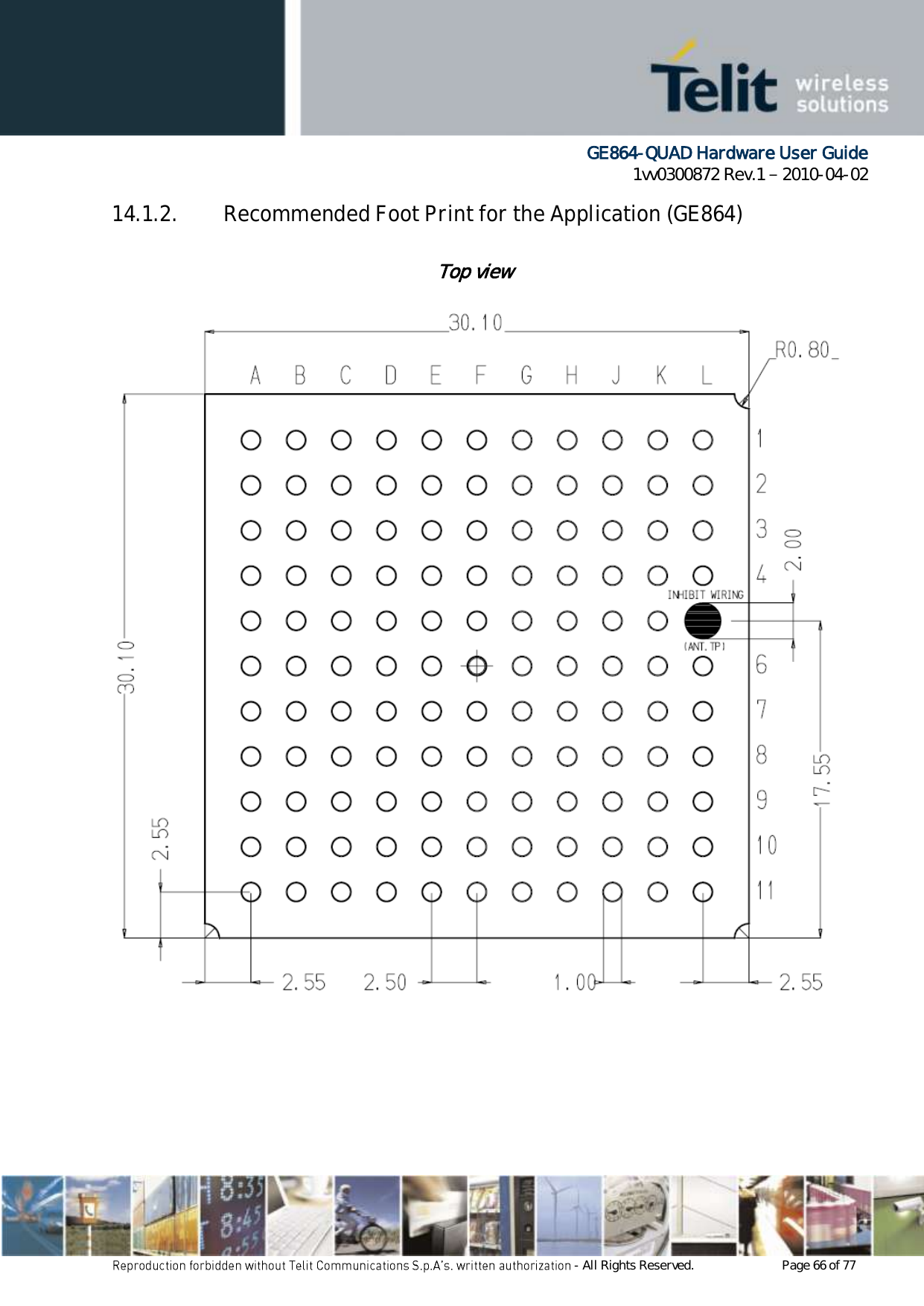
![GE864-QUAD Hardware User Guide 1vv0300872 Rev.1 2010-04-02 - All Rights Reserved. Page 63 of 77 13. DAC and ADC Section 13.1. DAC Converter 13.1.1. Description The GE864-QUAD module provides a Digital to Analog Converter. The signal (named DAC_OUT) is available on BGA Ball C7 of the GE864-QUAD module and on pin 17 of PL102 on EVK2 Board (CS1152). The on board DAC is a 10-bit converter, able to generate a analogue value based a specific input in the range from 0 up to 1023. However, an external low-pass filter is necessary Min Max Units Voltage range (filtered) 0 2,6 Volt Range 0 1023 Steps The precision is 10 bits so, if we consider that the maximum voltage is 2V, the integrated voltage could be calculated with the following formula: Integrated output voltage = 2 * value / 1023 DAC_OUT line must be integrated (for example with a low band pass filter) in order to obtain an analog voltage. 13.1.2. Enabling DAC The AT command below is available to use the DAC function: AT#DAC[=<enable>[,<value>]] <value> – scale factor of the integrated output voltage (0..1023 – 10 bit precision) it must be present if <enable>=1 Refer to SW User Guide or AT Commands Reference Guide for the full description of this function. NOTE: The DAC frequency is selected internally. D/A converter must not be used during POWERSAVING.](https://usermanual.wiki/Telit-Communications-S-p-A/GE864QC2/User-Guide-1270202-Page-63.png)
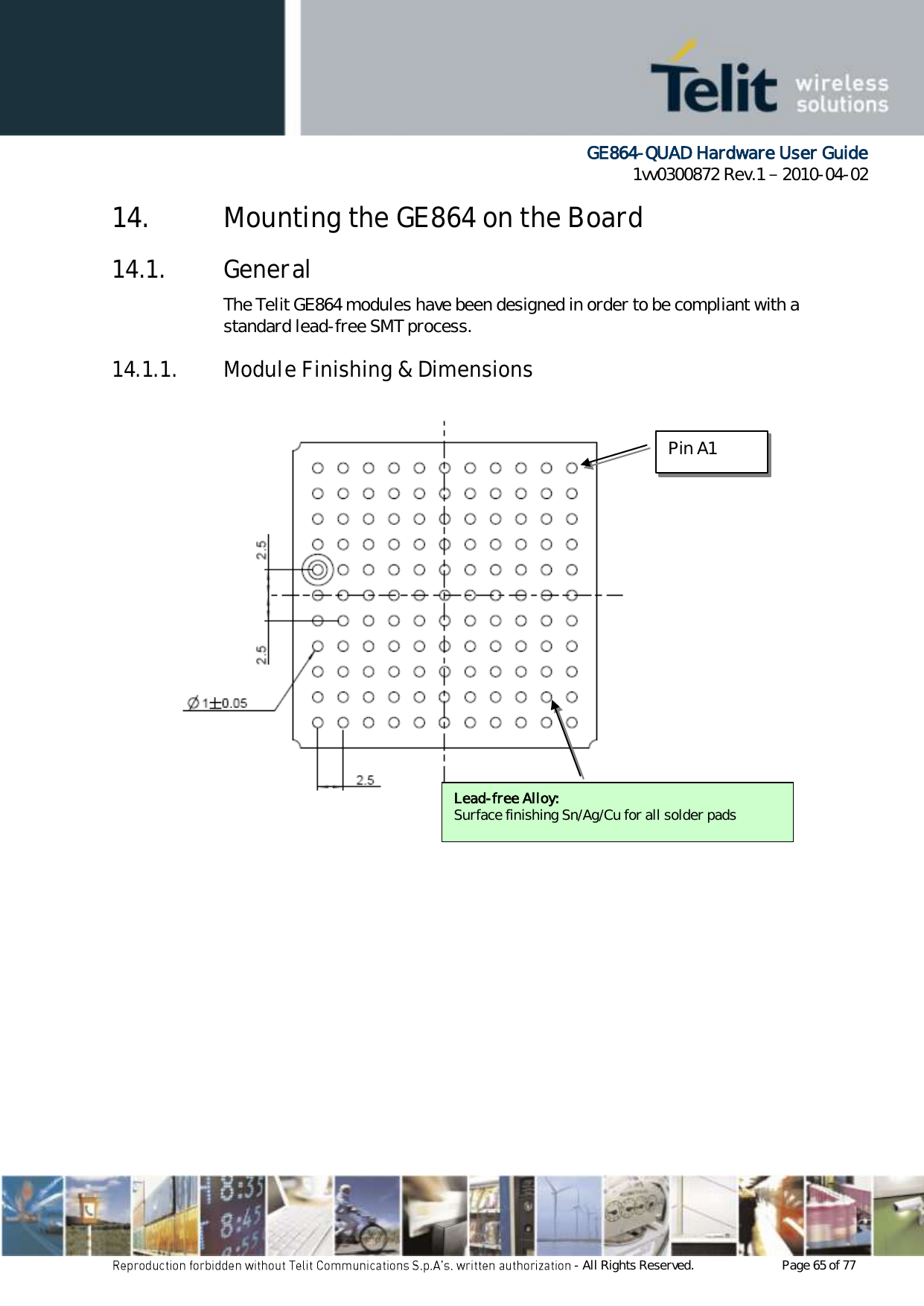
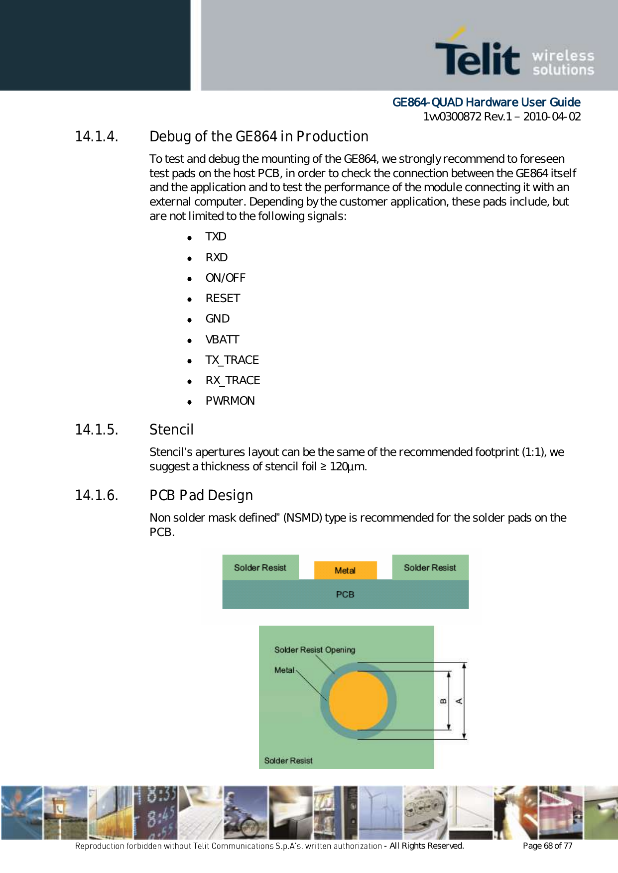
![GE864-QUAD Hardware User Guide 1vv0300872 Rev.1 2010-04-02 - All Rights Reserved. Page 69 of 77 Recommendations for PCB pad dimensions: Ball pitch [mm] 2,5 Solder resist opening diameter A [mm] 1,150 Metal pad diameter B [mm] 1 ± 0.05 It is recommended no microvia without solder resist cover under the module and no microvia around the pads (see following figure). Holes in pad are allowed only for blind holes and not for through holes. Recommendations for PCB pad surfaces: Finish Layer thickness [µm] Properties Electro-less Ni / Immersion Au 3 7 / 0.05 0.15 good solder ability protection, high shear force values The PCB must be able to resist the higher temperatures which are occurring at the lead-free process. This issue must be discussed with the PCB-supplier. Generally, the wettability of tin-lead solder paste on the described surface plating is better compared to lead-free solder paste. 14.1.7. Solder Paste Lead free Solder paste Sn/Ag/Cu](https://usermanual.wiki/Telit-Communications-S-p-A/GE864QC2/User-Guide-1270202-Page-69.png)