Telit Communications S p A GE866 Wireless module User Manual 1VV0301051 GE866 QUAD Hardware User Guide r2
Telit Communications S.p.A. Wireless module 1VV0301051 GE866 QUAD Hardware User Guide r2
UserManual.wiki
>
Telit Communications S p A
>
GE866 User Manual
User Manual
Navigation menu
Upload a User Manual
Namespaces
Wiki Guide
HTML
PDF
Info
Views
User Manual
Discussion / Help
Navigation


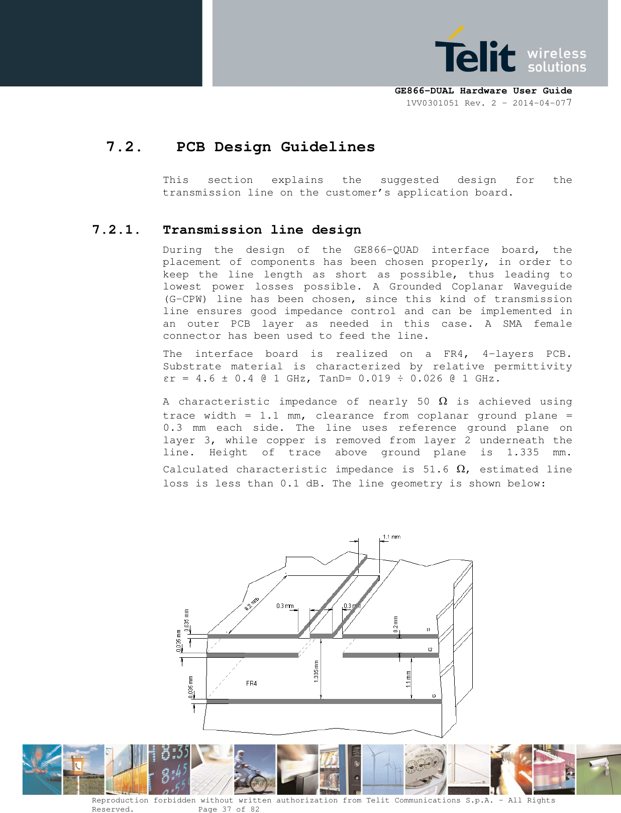
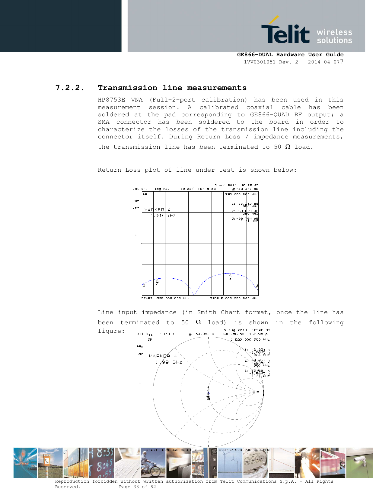
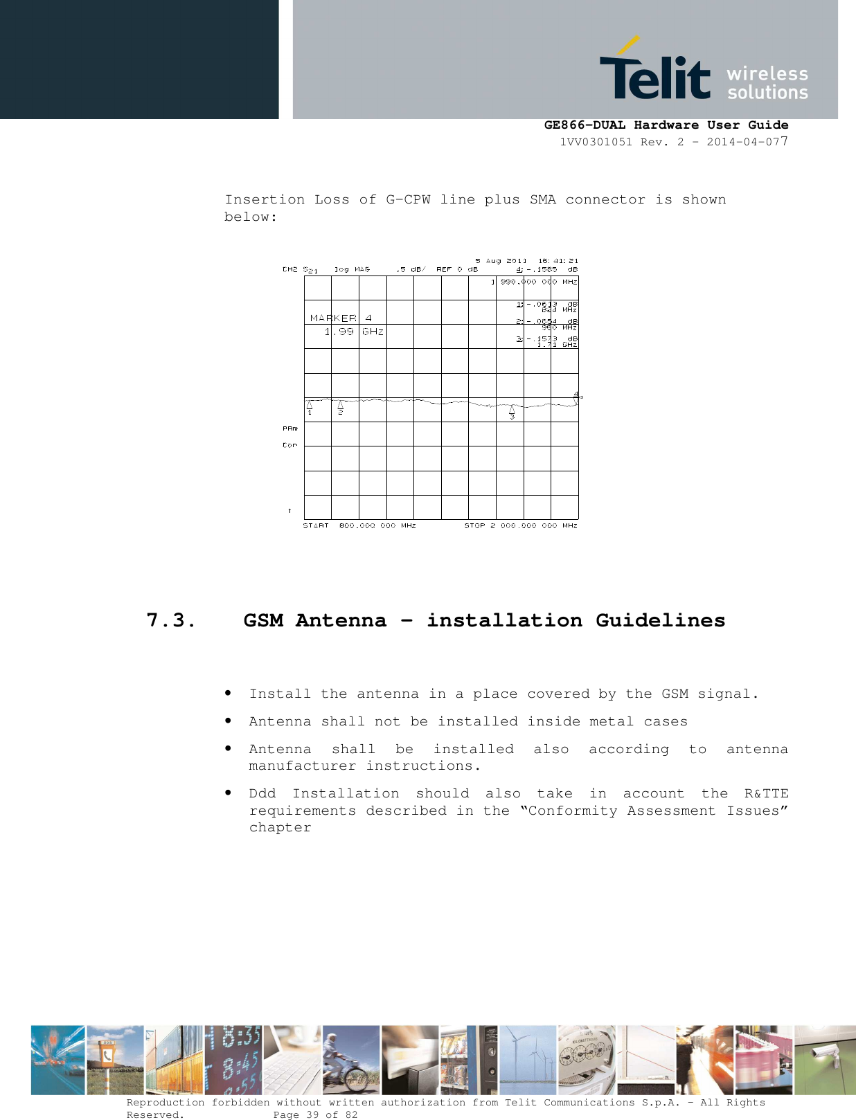
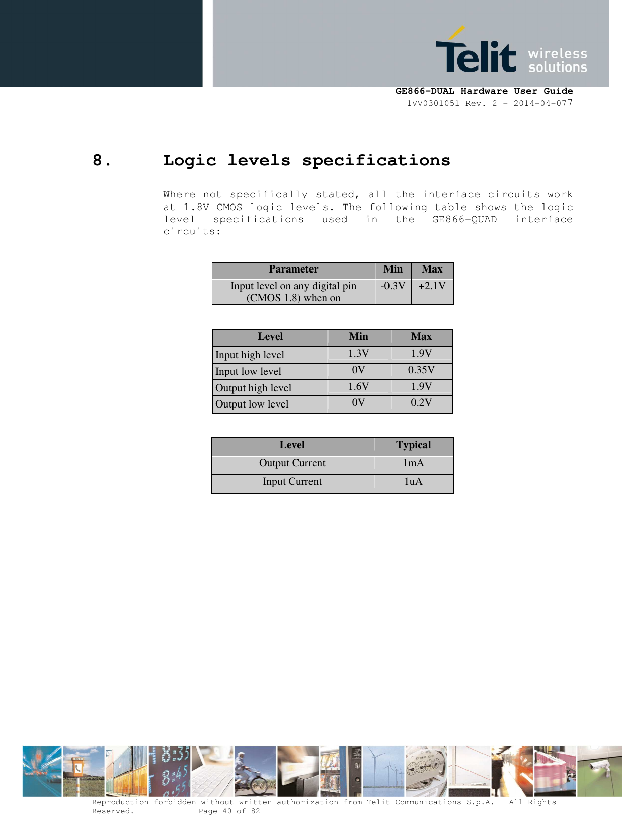

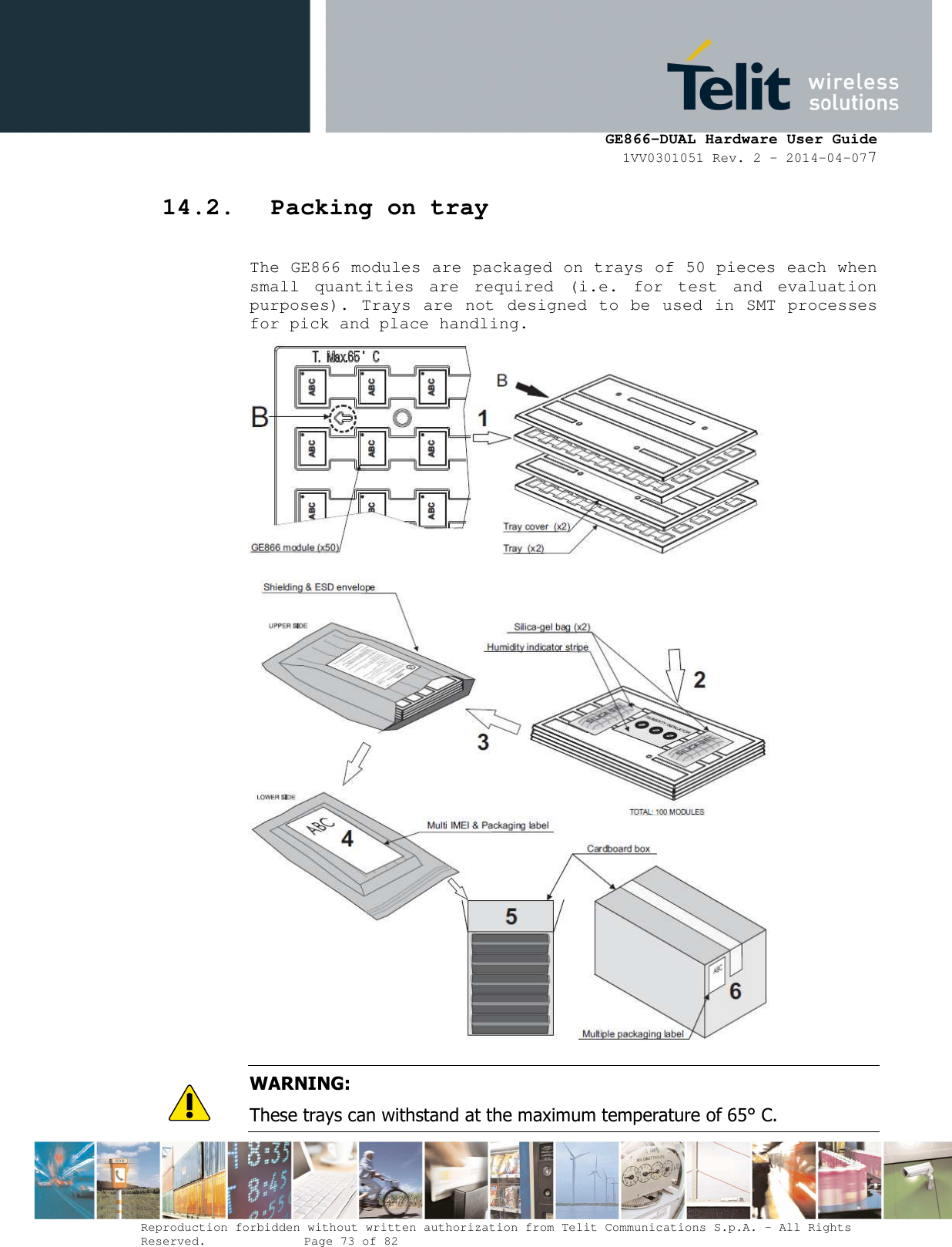
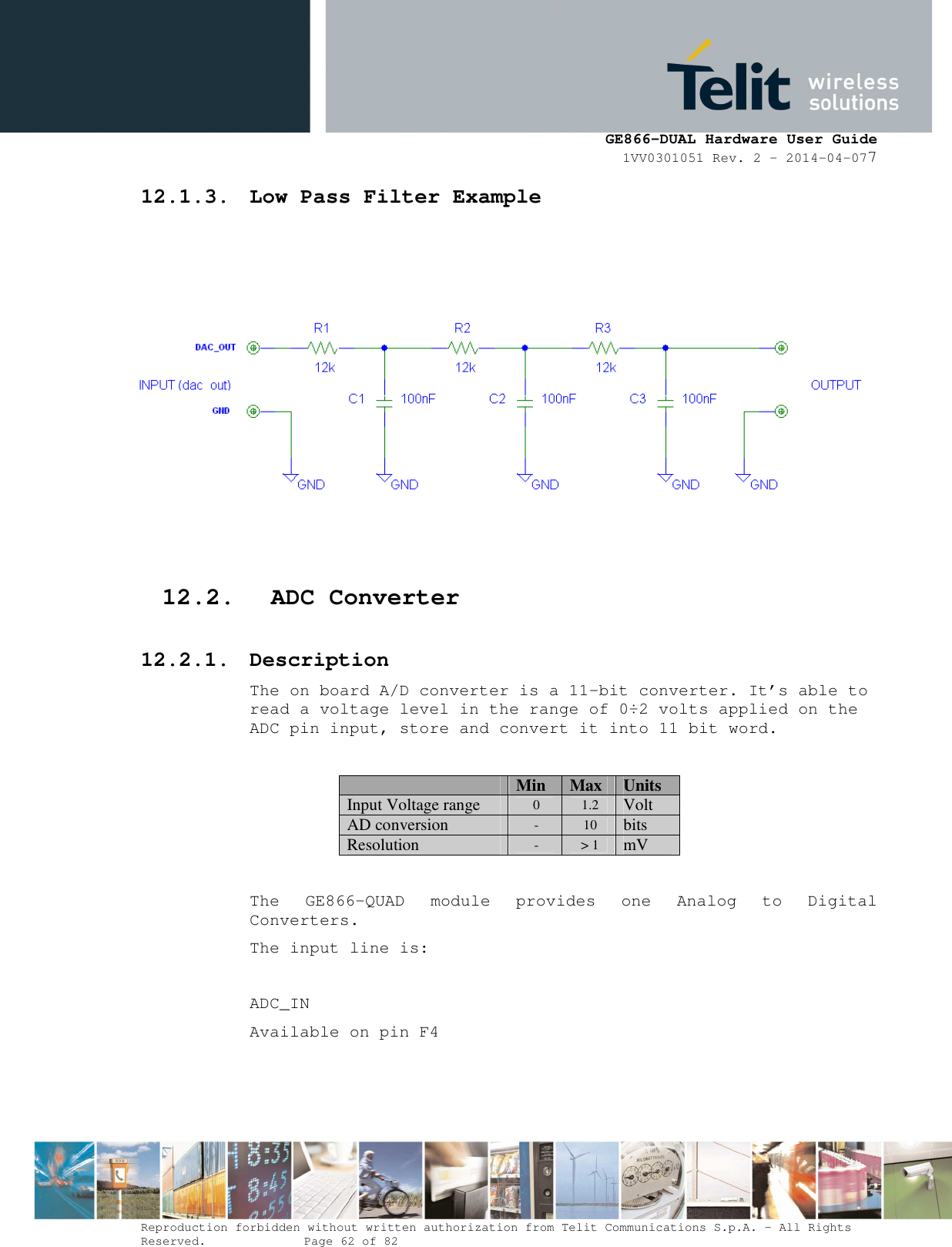
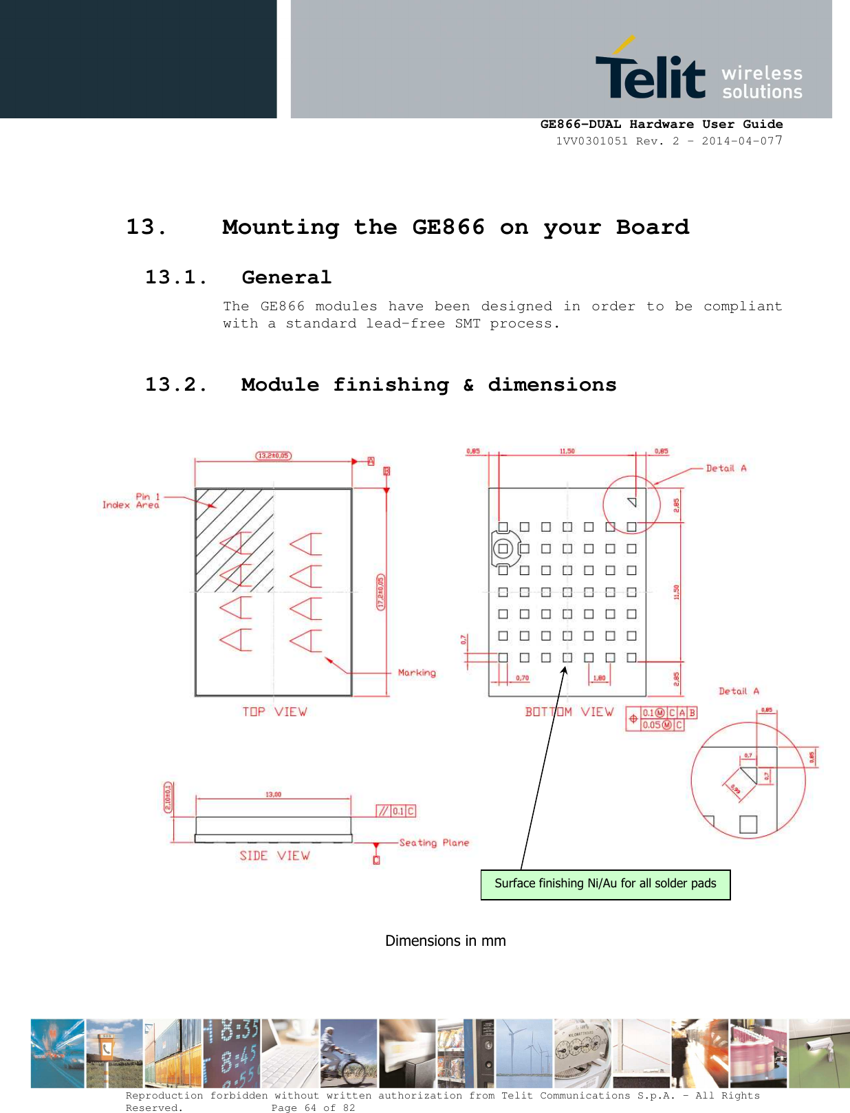
![GE866-DUAL Hardware User Guide 1VV0301051 Rev. 2 – 2014-04-077 Reproduction forbidden without written authorization from Telit Communications S.p.A. - All Rights Reserved. Page 61 of 82 Mod. 0805 2011-07 Rev.2 12. DAC and ADC section 12.1. DAC Converter 12.1.1. Description The GE866-QUAD provides a Digital to Analog Converter. The signal (named DAC_OUT) is available on pin E4 of the GE866-QUAD. The on board DAC is a 10 bit converter, able to generate an analogue value based on a specific input in the range from 0 up to 1023. However, an external low-pass filter is necessary Min Max Units Voltage range (filtered) 0 1.8 Volt Range 0 1023 Steps The precision is 10 bits so, if we consider that the maximum voltage is 2V, the integrated voltage could be calculated with the following formula: Integrated output voltage = (2 *value) / 1023 DAC_OUT line must be integrated (for example with a low band pass filter) in order to obtain an analog voltage. 12.1.2. Enabling DAC An AT command is available to use the DAC function. The command is: AT#DAC= [<enable> [, <value>]] <value> - scale factor of the integrated output voltage (0..1023 - 10 bit precision) it must be present if <enable>=1 Refer to SW User Guide or AT Commands Reference Guide for the full description of this function. NOTE: The DAC frequency is selected internally. D/A converter must not be used during POWERSAVING.](https://usermanual.wiki/Telit-Communications-S-p-A/GE866/User-Guide-2260503-Page-61.png)
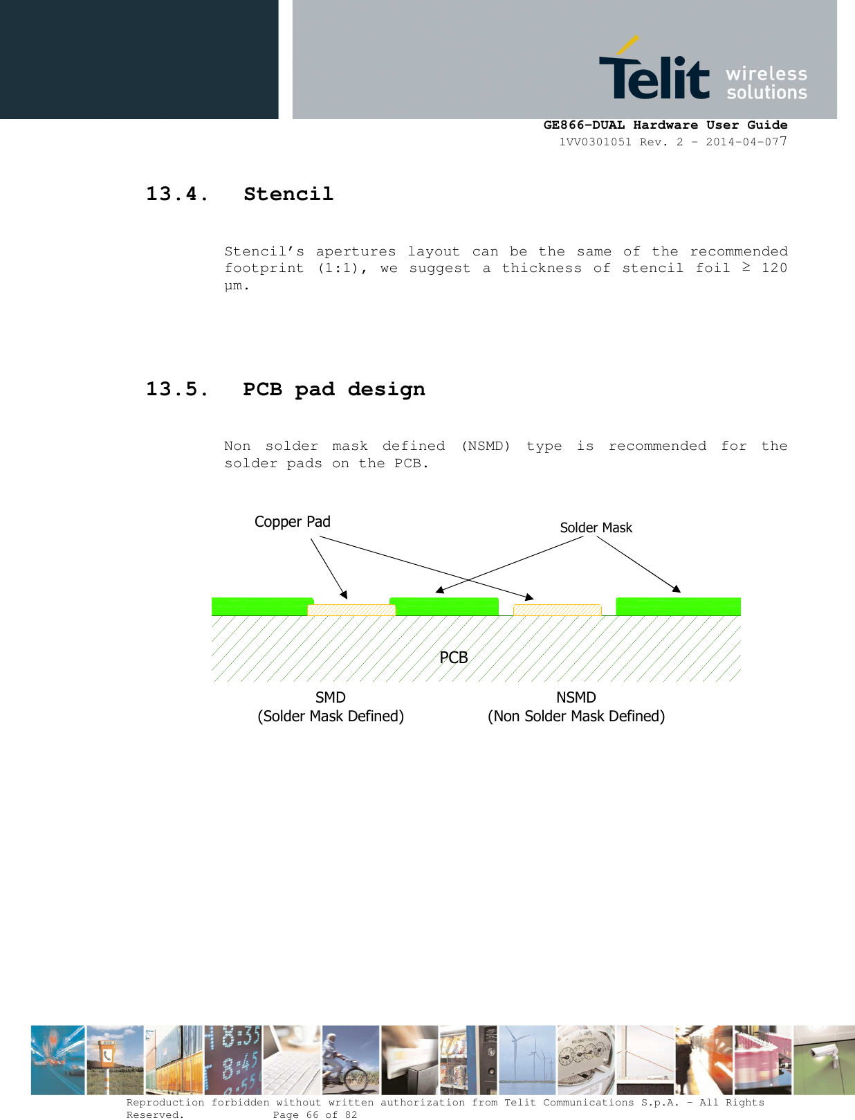
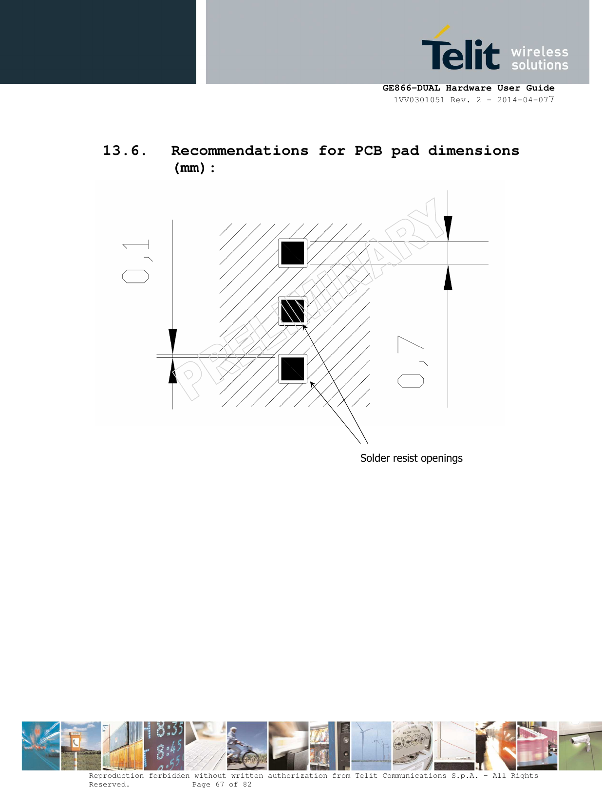
![GE866-DUAL Hardware User Guide 1VV0301051 Rev. 2 – 2014-04-077 Reproduction forbidden without written authorization from Telit Communications S.p.A. - All Rights Reserved. Page 68 of 82 Mod. 0805 2011-07 Rev.2 It is not recommended to place via or micro-via not covered by solder resist in an area of 0,3 mm around the pads unless it carries the same signal of the pad itself (see following figure). Holes in pad are allowed only for blind holes and not for through holes. Recommendations for PCB pad surfaces: Finish Layer thickness [µm] Properties Electro-less Ni / Immersion Au 3 –7 / 0.05 – 0.15 good solder ability protection, high shear force values The PCB must be able to resist the higher temperatures which are occurring at the lead-free process. This issue should be discussed with the PCB-supplier. Generally, the wettability of Inhibit area for micro-via](https://usermanual.wiki/Telit-Communications-S-p-A/GE866/User-Guide-2260503-Page-68.png)