Telit Communications S p A GM862 Data Terminal Module User Manual
Telit Communications S.p.A. Data Terminal Module
User Manual

Telit GM862-QUAD/-QUAD-PY
Hardware User Guide
1vv0300692, Rev. ISSUE#0, - 04/10/2005
Reproduction forbidden without DAI Telecom written authorization – All Right reserved – Right of modification reserved page 1 of 69
T
Te
el
li
it
t
G
GM
M8
86
62
2-
-Q
QU
UA
AD
D
G
GM
M8
86
62
2-
-Q
QU
UA
AD
D-
-P
PY
Y
H
Ha
ar
rd
dw
wa
ar
re
e
U
Us
se
er
r
G
Gu
ui
id
de
e
Telit Communications S.p.A. 2005

Telit GM862-QUAD/-QUAD-PY
Hardware User Guide
1vv0300692, Rev. ISSUE#0, - 04/10/2005
Reproduction forbidden without DAI Telecom written authorization – All Right reserved – Right of modification reserved page 2 of 69
Contents
1 OVERVIEW 4
2 HARDWARE COMMANDS 5
2.1 Turning ON the GM862-QUAD 5
2.2 Turning OFF the GM862-QUAD 7
2.2.1.1 Hardware shutdown 7
2.2.1.2 Hardware Unconditional Reset 7
3 POWER SUPPLY 9
3.1 Power Supply Requirements 9
3.2 General Design Rules 9
3.2.1 Electrical design Guidelines 10
3.2.1.1 + 5V input Source Power Supply Design Guidelines 10
3.2.1.2 + 12V input Source Power Supply Design Guidelines 11
3.2.1.3 Battery Source Power Supply Design Guidelines 12
3.2.1.4 Battery Charge control Circuitry Design Guidelines 12
3.2.2 Thermal Design Guidelines 14
3.2.3 Power Supply PCB layout Guidelines 15
4 SERIAL PORT 17
4.1 RS232 level translation 19
4.2 5V UART level translation 21
5 MICROPHONE 23
5.1 Microphone line Characteristic and requirements 23
5.2 General Design Rules 26
5.3 Microphone Biasing 26
5.3.1 Balanced Microphone biasing 27
5.3.2 Unbalanced Microphone biasing 28
5.4 Microphone buffering 29
5.4.1 Buffered Balanced Mic. 29
5.4.2 Buffered Unbalanced (Single Ended) Mic. 31

Telit GM862-QUAD/-QUAD-PY
Hardware User Guide
1vv0300692, Rev. ISSUE#0, - 04/10/2005
Reproduction forbidden without DAI Telecom written authorization – All Right reserved – Right of modification reserved page 3 of 69
6 SPEAKER 34
6.1 Speaker lines characteristics and requirements 34
6.2 General Design rules 36
6.2.1 Noise Filtering 36
6.3 Handset earphone design 36
6.4 Hands Free earphone (low power) design 38
6.5 Car Kit speakerphone design 38
7 GENERAL PURPOSE I/O 40
7.1 Using a GPIO pin as INPUT 40
7.2 Using a GPIO pin as OUTPUT 40
7.3 Using the Alarm Output GPIO6 41
7.4 Using the Buzzer Output GPIO7 41
8 CAMERA 42
8.1 Agilent Camera 42
8.1.1 Camera interface connectors 42
8.1.2 EVB for camera support 44
8.2 Camera Transchip 45
8.2.1 Camera interface connectors 45
8.2.2 EVB for Agilent and Transchip camera support 47
8.2.3 Block Diagram for supported cameras 48
8.2.4 Schematic Diagrams for supported cameras 49
8.2.5 Example usage script for camera 51
9 DOCUMENT CHANGE LOG 52
10 ANNEX A - EVK SCHEMATICS 53
11 ANNEX B - CAMERA EVB SCHEMATICS 65

Telit GM862-QUAD/-QUAD-PY
Hardware User Guide
1vv0300692, Rev. ISSUE#0, - 04/10/2005
Reproduction forbidden without DAI Telecom written authorization – All Right reserved – Right of modification reserved page 4 of 69
1 Overview
The aim of this document is the description of some hardware solutions useful for developing a
product with the Telit GM862-QUAD/-QUAD-PY modules.
In this document all the basic functions of a mobile phone will be taken into account; for each one
of them a proper hardware solution will be suggested and eventually the wrong solutions and
common errors to be avoided will be evidenced. Obviously this document can not embrace the
whole hardware solutions and products that may be designed. The wrong solutions to be avoided
shall be considered as mandatory, while the suggested hardware configurations shall not be
considered mandatory, instead the information given shall be used as a guide and a starting point for
properly developing your product with the Telit GM862-QUAD/-QUAD-PY modules. For further
hardware details that may not be explained in this document refer to the GM862-QUAD/-QUAD-
PY Product Description document where all the hardware information is reported.
NOTE: In this document all the hardware solution are referenced to the GM862-QUAD.
As a general rule, since all the product line GM862-QUAD, GM862-QUAD-PY is pin to pin
hardware compatible, all these solutions apply also to the GM862-QUAD-PY.
NOTE
The information presented in this document is believed to be accurate and reliable. However, no responsibility is
assumed by DAI Telecom for its use, nor any infringement of patents or other rights of third parties which may result
from its use. No license is granted by implication or otherwise under any patent rights of DAI Telecom other than for
circuitry embodied in Telit products. This document is subject to change without notice.
Telit GM862-QUAD/-QUAD-PY
Hardware User Guide
1vv0300692, Rev. ISSUE#0, - 04/10/2005
Reproduction forbidden without DAI Telecom written authorization – All Right reserved – Right of modification reserved page 5 of 69
2 Hardware Commands
2.1 Turning ON the GM862-QUAD
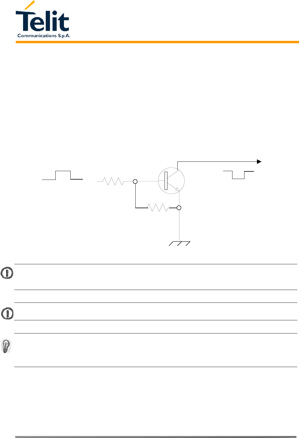
To turn on the GM862-QUAD the pin ON# must be tied low for at least 1 second and then released.
The maximum current that can be drained from the ON# pin is 0,1 mA.
A simple circuit to do it is:
NOTE: don't use any pull up resistor on the ON# line, it is internally pulled up. Using pull up resistor
may bring to latch up problems on the GM862-QUAD power regulator and improper power on/off of the
module. The line ON# must be connected only in open collector configuration.
NOTE: In this document all the lines that are inverted, hence have active low signals are labeled with a
name that ends with a "#" or with a bar over the name.
TIP: To check if power has raised it is possible to monitor the START line, when this line goes high the
module is powered on, but before it remains on the device needs other 900 ms for software startup.
Hence check the PWRCTL line and 900 ms after its transition to high it is possible to release the ON#
pin.
ON#
Power ON impulse
GND
R1
R2
Q1
Telit GM862-QUAD/-QUAD-PY
Hardware User Guide
1vv0300692, Rev. ISSUE#0, - 04/10/2005
Reproduction forbidden without DAI Telecom written authorization – All Right reserved – Right of modification reserved page 6 of 69
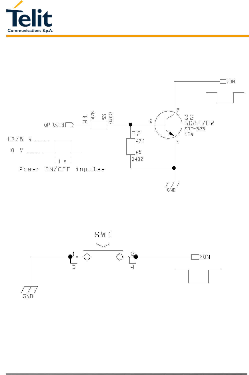
For example:
1- Let's assume you need to drive the ON# pin with a totem pole output of a +3/5 V microcontroller
(uP_OUT1):
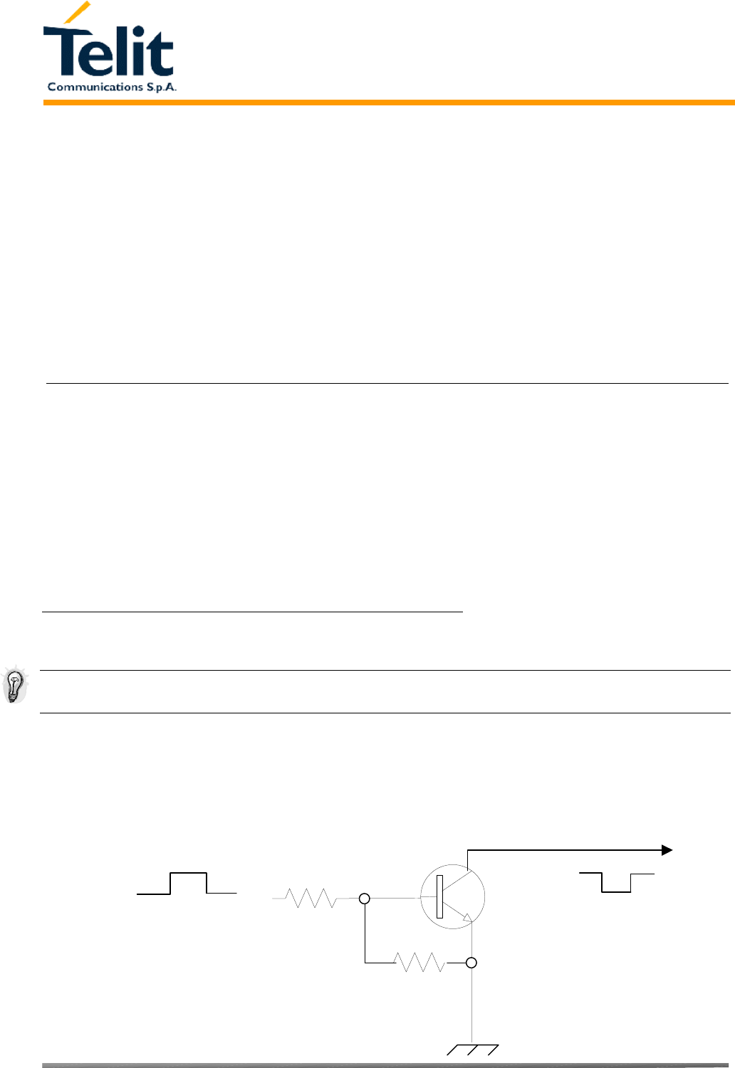
2- Let's assume you need to drive the ON# pin directly with an ON/OFF button:
Telit GM862-QUAD/-QUAD-PY
Hardware User Guide
1vv0300692, Rev. ISSUE#0, - 04/10/2005
Reproduction forbidden without DAI Telecom written authorization – All Right reserved – Right of modification reserved page 7 of 69
2.2 Turning OFF the GM862-QUAD
The turning off of the device can be done in three ways:
• by software command (see GM862-QUAD Software User Guide)
• by hardware shutdown
• by hardware unconditional shutdown
When the device is shut down by software command or by hardware shutdown, it issues to the
network a detach request that informs the network that the device will not be reachable any more.
The hardware unconditional shutdown does not issue this request and shuts down immediately the
device.
The hardware unconditional shutdown must not be used during normal operation of the device
since it does not detach the device from the network. It shall be kept as an emergency exit
procedure to be done in the rare case that the device gets stucked waiting for some network or SIM
responses.
If device does not respond to a command in the timeout window, retry issuing the command and if
still no response is received a hardware unconditional shutdown shall be issued and then a restart.
2.2.1.1 Hardware shutdown
To turn OFF the GM862-QUAD the pin ON# must be tied low for at least 1 second and then
released.
The same circuitry and timing for the power on shall be used.
The device shuts down after the release of the ON# pin.
TIP: To check if the device has powered off, the hardware line PWRCTL should be monitored. When
PWRCTL goes low, the device has powered off.
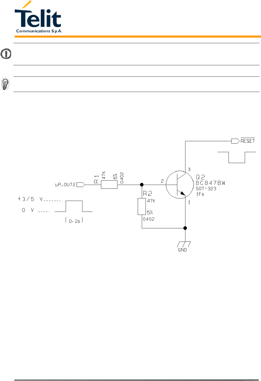
2.2.1.2 Hardware Unconditional Reset
To unconditionally turn OFF the GM862-QUAD the pin RESET# must be tied low for at least 200
milliseconds and then released.
The maximum current that can be drained from the ON# pin is 0,15 mA.
A simple circuit to do it is:
RESET#
Unconditional Power OFF
impulse
GND
Telit GM862-QUAD/-QUAD-PY
Hardware User Guide
1vv0300692, Rev. ISSUE#0, - 04/10/2005
Reproduction forbidden without DAI Telecom written authorization – All Right reserved – Right of modification reserved page 8 of 69
NOTE: don't use any pull up resistor on the RESET# line nor any totem pole digital output. Using pull
up resistor may bring to latch up problems on the GM862-QUAD power regulator and improper
functioning of the module. The line RESET# must be connected only in open collector configuration.
TIP: The unconditional hardware reset should be always implemented on the boards and software
should use it as an emergency exit procedure.
For example:
1- Let's assume you need to drive the RESET# pin with a totem pole output of a +3/5 V
microcontroller (uP_OUT2):
Unconditional Reset
impulse

Telit GM862-QUAD/-QUAD-PY
Hardware User Guide
1vv0300692, Rev. ISSUE#0, - 04/10/2005
Reproduction forbidden without DAI Telecom written authorization – All Right reserved – Right of modification reserved page 9 of 69
3 Power Supply
The power supply circuitry and board layout are the most important part in the full product design
and they strongly reflect on the product overall performances, hence read carefully the requirements
and the guidelines that will follow for a proper design.
3.1 Power Supply Requirements
The GM862-QUAD power requirements are:
• Nominal Supply Voltage: 3.8 V
• Max Supply Voltage: 4.2 V
• Supply voltage range: 3.4 V - 4.2 V
• Max Peak current consumption (impulsive): 1.9 A
• Max Average current consumption during transmission (rms): 350 mA
• Average current during Power Saving: ≈ 4 mA
• Average current during idle (Power Saving disabled) ≈ 17 mA
The GSM system is made in a way that the RF transmission is not continuous, else it is packed into
bursts at a base frequency of about 216 Hz, the relative current peaks can be as high as about 2A.
Therefore the power supply has to be designed in order to withstand with these current peaks
without big voltage drops; this means that both the electrical design and the board layout must be
designed for this current flow.
If the layout of the PCB is not well designed a strong noise floor is generated on the ground and the
supply; this will reflect on all the audio paths producing an audible annoying noise at 216 Hz; if the
voltage drop during the peak current absorption is too much, then the device may even shutdown as
a consequence of the supply voltage drop.
TIP: The electrical design for the Power supply should be made ensuring it will be capable of a peak
current output of at least 2 A.
3.2 General Design Rules
The principal guidelines for the Power Supply Design embrace three different design steps:
- the electrical design
- the thermal design.
- the PCB layout.
Telit GM862-QUAD/-QUAD-PY
Hardware User Guide
1vv0300692, Rev. ISSUE#0, - 04/10/2005
Reproduction forbidden without DAI Telecom written authorization – All Right reserved – Right of modification reserved page 10 of 69
3.2.1 Electrical design Guidelines
The electrical design of the power supply depends strongly from the power source where this power
is drained. We will distinguish them into three categories:
• +5V input (typically PC internal regulator output)
• +12V input (typically automotive)
• Battery
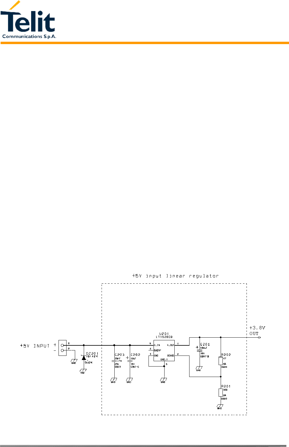
3.2.1.1 + 5V input Source Power Supply Design Guidelines
• The desired output for the power supply is 3.8V, hence there's not a big difference between the
input source and the desired output and a linear regulator can be used. A switching power
supply will not be suited because of the low drop out requirements.
• When using a linear regulator, a proper heat sink shall be provided in order to dissipate the
power generated.
• A Bypass low ESR capacitor of adequate capacity must be provided in order to cut the current
absorption peaks close to the GM862-QUAD, a 100μF tantalum capacitor is usually suited.
• Make sure the low ESR capacitor on the power supply output (usually a tantalum one) is rated
at least 10V.
• A protection diode should be inserted close to the power input, in order to save the GM862-
QUAD from power polarity inversion.
An example of linear regulator with 5V input is:
Telit GM862-QUAD/-QUAD-PY
Hardware User Guide
1vv0300692, Rev. ISSUE#0, - 04/10/2005
Reproduction forbidden without DAI Telecom written authorization – All Right reserved – Right of modification reserved page 11 of 69
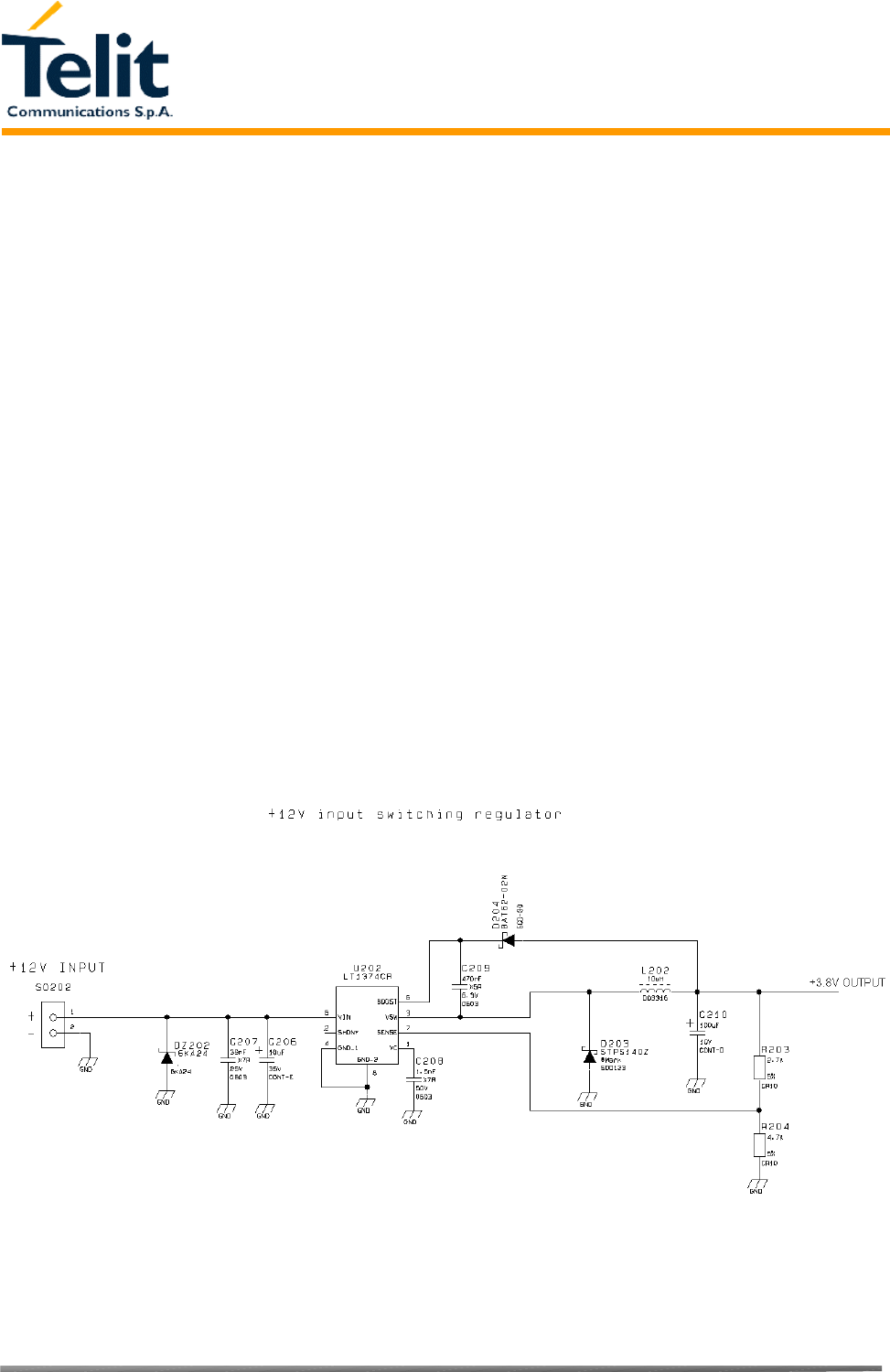
3.2.1.2 + 12V input Source Power Supply Design Guidelines
• The desired output for the power supply is 3.8V, hence due to the big difference between the
input source and the desired output, a linear regulator is not suited and shall not be used. A
switching power supply will be preferable because of its better efficiency especially with the 2A
peak current load represented by the GM862-QUAD.
• When using a switching regulator, a 500Khz switching frequency regulator is preferable
because of its smaller inductor size and its faster transient response. This allows the regulator to
respond quickly to the current peaks absorption.
• For car PB battery the input voltage can rise up to 15,8V and this should be kept in mind when
choosing components: all components in the power supply must withstand this voltage.
• A Bypass low ESR capacitor of adequate capacity must be provided in order to cut the current
absorption peaks, a 100μF tantalum capacitor is usually suited.
• Make sure the low ESR capacitor on the power supply output (usually a tantalum one) is rated
at least 10V.
• For Car applications a spike protection diode should be inserted close to the power input, in
order to clean the supply from spikes.
• A protection diode should be inserted close to the power input, in order to save the GM862-
QUAD from power polarity inversion. This can be the same diode as for spike protection.
An example of switching regulator with 12V input is:

Telit GM862-QUAD/-QUAD-PY
Hardware User Guide
1vv0300692, Rev. ISSUE#0, - 04/10/2005
Reproduction forbidden without DAI Telecom written authorization – All Right reserved – Right of modification reserved page 12 of 69
3.2.1.3 Battery Source Power Supply Design Guidelines
• The desired nominal output for the power supply is 3.8V and the maximum voltage allowed is
4.2V, hence a single 3.7V Li-Ion cell battery type is suited for supplying the power to the Telit
GM862-QUAD module.
The three cells Ni/Cd or Ni/MH 3,6 V Nom. battery types or 4V PB types MUST NOT BE
USED since their maximum voltage can rise over the absolute maximum voltage for the
GM862-QUAD and damage it.
NOTE: DON'T USE any Ni-Cd, Ni-MH, and Pb battery types. Their use can lead to overvoltage on the
GM862-QUAD and damage it. USE ONLY Rechargeable Li-Ion battery types.
• A Bypass low ESR capacitor of adequate capacity must be provided in order to cut the current
absorption peaks, a 100μF tantalum capacitor is usually suited.
• Make sure the low ESR capacitor (usually a tantalum one) is rated at least 10V.
• A protection diode should be inserted close to the power input, in order to save the GM862-
QUAD from power polarity inversion. Otherwise the battery connector should be done in a way
to avoid polarity inversions when connecting the battery.
• The battery capacity must be at least 500mAh in order to withstand the current peaks of 2A; the
suggested capacity is from 500mAh to 1000mAh.
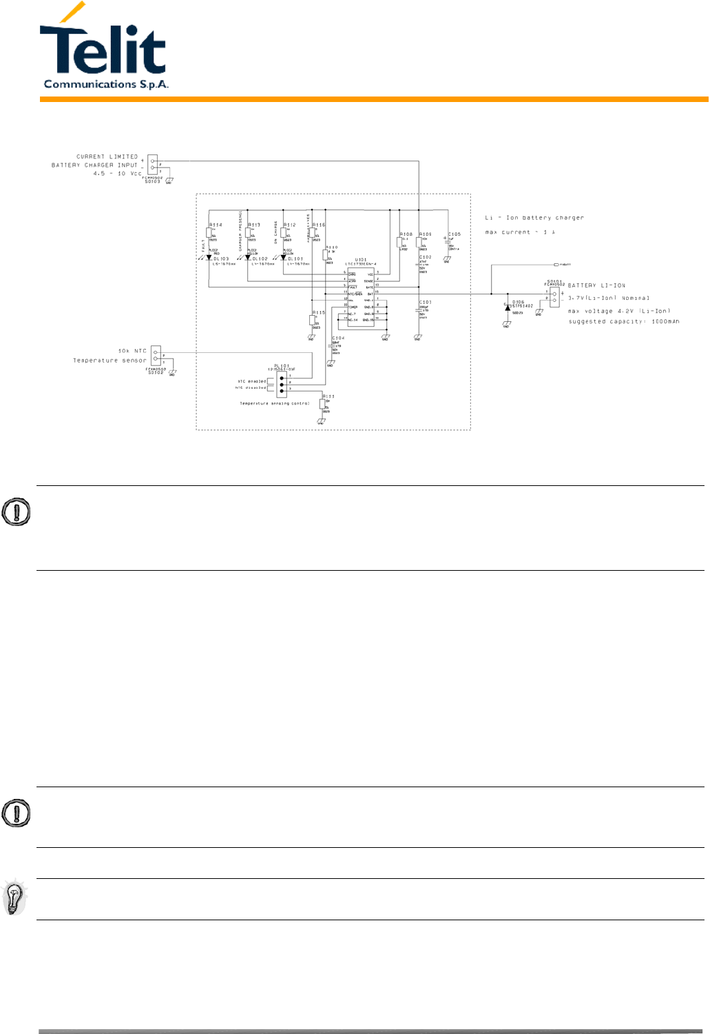
3.2.1.4 Battery Charge control Circuitry Design Guidelines
The charging process for Li-Ion Batteries can be divided into 4 phases:
• Qualification and trickle charging
• Fast charge 1 - constant current
• Final charge - constant voltage or pulsed charging
• Maintenance charge
The qualification process consists in a battery voltage measure, indicating roughly its charge status.
If the battery is deeply discharged, that means its voltage is lower than the trickle charging
threshold, then the charge must start slowly possibly with a current limited pre-charging process
where the current is kept very low with respect to the fast charge value: the trickle charging.
During the trickle charging the voltage across the battery terminals rises; when it reaches the fast
charge threshold level the charging process goes into fast charge phase.
During the fast charge phase the process proceeds with a current limited charging; this current limit
depends on the required time for the complete charge and from the battery pack capacity. During
this phase the voltage across the battery terminals still raises but at a lower rate.

Telit GM862-QUAD/-QUAD-PY
Hardware User Guide
1vv0300692, Rev. ISSUE#0, - 04/10/2005
Reproduction forbidden without DAI Telecom written authorization – All Right reserved – Right of modification reserved page 13 of 69
Once the battery voltage reaches its maximum voltage then the process goes into its third state:
Final charging. The voltage measure to change the process status into final charge is very
important. It must be ensured that the maximum battery voltage is never exceeded, otherwise the
battery may be damaged and even explode. Moreover for the constant voltage final chargers, the
constant voltage phase (final charge) must not start before the battery voltage has reached its
maximum value, otherwise the battery capacity will be highly reduced.
The final charge can be of two different types: constant voltage or pulsed.
The constant voltage charge proceeds with a fixed voltage regulator (very accurately set to the
maximum battery voltage) and hence the current will decrease while the battery is becoming
charged. When the charging current falls below a certain fraction of the fast charge current value,
then the battery is considered fully charged, the final charge stops and eventually starts the
maintenance.
The pulsed charge process has no voltage regulation, instead the charge continues with pulses.
Usually the pulse charge works in the following manner: the charge is stopped for some time, let's
say few hundreds of ms, then the battery voltage will be measured and when it drops below its
maximum value a fixed time length charging pulse is issued. As the battery approaches its full
charge the off time will become longer, hence the duty-cycle of the pulses will decrease. The
battery is considered fully charged when the pulse duty-cycle is less than a threshold value,
typically 10%, the pulse charge stops and eventually the maintenance starts.
The last phase is not properly a charging phase, since the battery at this point is fully charged and
the process may stop after the final charge. The maintenance charge provides an additional charging
process to compensate for the charge leak typical of a Li-Ion battery. It is done by issuing pulses
with a fixed time length, again few hundreds of ms, and a duty-cycle around 5% or less.
This last phase is not implemented in the GM862-QUAD internal charging algorithm, so that the
battery once charged is left discharging down to a certain threshold so that it is cycled from full
charge to slight discharge even if the battery charger is always inserted. This guarantees that
anyway the remaining charge in the battery is a good percentage and that the battery is not damaged
by keeping it always fully charged (Li-Ion rechargeable battery usually deteriorate when kept fully
charged).
Last but not least, in some applications it is highly desired that the charging process restarts when
the battery is discharged and its voltage drops below a certain threshold, GM862-QUAD internal
charger does it.
As you can see, the charging process is not a trivial task to be done; moreover all these operations
should start only if battery temperature is inside a charging range, usually 5°C - 45°C.
The GM862-QUAD measures the temperature of its internal component, in order to satisfy this last
requirement, it's not exactly the same as the battery temperature but in common application the two
temperature should not differ too much and the charging temperature range should be guaranteed.
Telit GM862-QUAD/-QUAD-PY
Hardware User Guide
1vv0300692, Rev. ISSUE#0, - 04/10/2005
Reproduction forbidden without DAI Telecom written authorization – All Right reserved – Right of modification reserved page 14 of 69
An example of battery charger can be:
NOTE: In this particular application the battery charger input current must be limited to less than 1A.
This can be done by using a current limited wall adapter as the power source.
For your convenience in the EVK there's also a current unlimited input, where the input source is not
limited in current and the drawn current is limited to about 0,5A by a MOSFET in the EVK.
3.2.2Thermal Design Guidelines
The thermal design for the power supply heat sink should be done with the following specifications:
• Average current consumption during transmission @PWR level max (rms): 350mA
• Average current consumption during transmission @ PWR level min (rms): 100mA
• Average current during Power Saving: 4mA
• Average current during idle (Power Saving disabled) 17mA
NOTE: The average consumption during transmissions depends on the power level at which the
device is requested to transmit by the network. The average current consumption hence varies
significantly.
TIP: The thermal design for the Power supply should be made keeping a average consumption at the
max transmitting level during calls of 350mA rms.
Considering the very low current during idle, especially if Power Saving function is enabled, it is
possible to consider from the thermal point of view that the device absorbs current significantly
only during calls.

Telit GM862-QUAD/-QUAD-PY
Hardware User Guide
1vv0300692, Rev. ISSUE#0, - 04/10/2005
Reproduction forbidden without DAI Telecom written authorization – All Right reserved – Right of modification reserved page 15 of 69
If we assume that the device stays into transmission for short periods of time (let's say few minutes)
and then remains for a quite long time in idle (let's say one hour), then the power supply has always
the time to cool down between the calls and the heat sink could be smaller than the calculated one
for 350mA maximum RMS current, or even could be the simple chip package (no heat sink).
Moreover in the average network conditions the device is requested to transmit at a lower power
level than the maximum and hence the current consumption will be less than the 350mA, being
usually around 150mA.
For these reasons the thermal design is rarely a concern and the simple ground plane where the
power supply chip is placed can be enough to ensure a good thermal condition and avoid
overheating.
3.2.3 Power Supply PCB layout Guidelines
As seen on the electrical design guidelines the power supply shall have a low ESR capacitor on the
output to cut the current peaks and a protection diode on the input to protect the supply from spikes
and polarity inversion. The placement of these components is crucial for the correct working of the
circuitry. A misplaced component can be useless or can even decrease the power supply
performances.
• The Bypass low ESR capacitor must be placed close to the Telit GM862-QUAD power input
pins or in the case the power supply is a switching type it can be placed close to the inductor to
cut the ripple provided the PCB trace from the capacitor to the GM862-QUAD is wide enough
to ensure a dropless connection even during the 2A current peaks.
• The protection diode must be placed close to the input connector where the power source is
drained.
• The PCB traces from the input connector to the power regulator IC must be wide enough to
ensure no voltage drops occur when the 2A current peaks are absorbed. Note that this is not
made in order to save power loss but especially to avoid the voltage drops on the power line at
the current peaks frequency of 216 Hz that will reflect on all the components connected to that
supply, introducing the noise floor at the burst base frequency. For this reason while a voltage
drop of 300-400 mV may be acceptable from the power loss point of view, the same voltage
drop may not be acceptable from the noise point of view. If your application doesn't have audio
interface but only uses the data feature of the Telit GM862-QUAD, then this noise is not so
disturbing and power supply layout design can be more forgiving.
• The PCB traces to the GM862-QUAD and the Bypass capacitor must be wide enough to ensure
no voltage drops occur when the 2A current peaks are absorbed. This is for the same reason as
previous point. Try to keep this trace as short as possible.
• The PCB traces connecting the Switching output to the inductor and the switching diode must
be kept as short as possible by placing the inductor and the diode very close to the power
switching IC (only for switching power supply). This is done in order to reduce the radiated
field (noise) at the switching frequency (100-500 kHz usually).
• The use of a good common ground plane is suggested.

Telit GM862-QUAD/-QUAD-PY
Hardware User Guide
1vv0300692, Rev. ISSUE#0, - 04/10/2005
Reproduction forbidden without DAI Telecom written authorization – All Right reserved – Right of modification reserved page 16 of 69
• The placement of the power supply on the board should be done in such a way to guarantee that
the high current return paths in the ground plane are not overlapped to any noise sensitive
circuitry as the microphone amplifier/buffer or earphone amplifier.
• The power supply input cables should be kept separate from noise sensitive lines such as
microphone/earphone cables.
Telit GM862-QUAD/-QUAD-PY
Hardware User Guide
1vv0300692, Rev. ISSUE#0, - 04/10/2005
Reproduction forbidden without DAI Telecom written authorization – All Right reserved – Right of modification reserved page 17 of 69
4 Serial Port
The serial port on the Telit GM862-QUAD is the core of the interface between the module and
OEM hardware. Several configurations can be designed for the serial port on the OEM hardware,
but the most common are:
- RS232 PC com port
- microcontroller UART @ 2.8V - 3V (Universal Asynchronous Receive Transmit)
- microcontroller UART@ 5V or other voltages different from 2.8V
Depending from the type of serial port on the OEM hardware a level translator circuit may be
needed to make the system work. The only configuration that doesn't need a level translation is the
2.8V UART.
The serial port on the GM862-QUAD is a +2.8V UART with all the 7 RS232 signals. It differs
from the PC-RS232 in the signal polarity (RS232 is reversed) and levels. The levels for the GM862-
QUAD UART are the CMOS levels:
Absolute Maximum Ratings -Not Functional
Parameter Min Max
Input level on any
digital pin when on
-0.3V +3.75V
Input voltage on
analog pins when on
-0.3V +3.0 V
Operating Range - Interface levels (2.8V CMOS)
Level Min Max
Input high level VIH 2.1V 3.3V
Input low level VIL 0V 0.5V
Output high level VOH 2.2V 3.0V
Output low level VOL 0V 0.35V

Telit GM862-QUAD/-QUAD-PY
Hardware User Guide
1vv0300692, Rev. ISSUE#0, - 04/10/2005
Reproduction forbidden without DAI Telecom written authorization – All Right reserved – Right of modification reserved page 18 of 69
The signals of the GM862-QUAD serial port are:
RS232
Pin
Number
Signal GM862-
QUAD
Pin
Number
Name Usage
1 DCD -
dcd_uart
36 Data Carrier Detect Output from the GM862-QUAD that
indicates the carrier presence
2 RXD -
tx_uart
37 Transmit line *see Note Output transmit line of GM862-QUAD
UART
3 TXD -
rx_uart
20 Receive line *see Note Input receive of the GM862-QUAD
UART
4 DTR -
dtr_uart
43 Data Terminal Ready Input to the GM862-QUAD that controls
the DTE READY condition
5 GND 2-4-6-8 Ground ground
6 DSR -
dsr_uart
33 Data Set Ready Output from the GM862-QUAD that
indicates the module is ready
7 RTS -
rts_uart
45 Request to Send Input to the GM862-QUAD that controls
the Hardware flow control
8 CTS -
cts_uart
29 Clear to Send Output from the GM862-QUAD that
controls the Hardware flow control
9 RI -
ri_uart
30 Ring Indicator Output from the GM862-QUAD that
indicates the incoming call condition
NOTE: According to V.24, RX/TX signal names are referred to the application side, therefore on the
GM862-QUAD side these signal are on the opposite direction: TXD on the application side will be
connected to the receive line (here named TXD/ rx_uart ) of the GM862-QUAD serial port and viceversa
for RX.
TIP: For a minimum implementation, only the TXD and RXD lines can be connected, the other lines can
be left open provided a software flow control is implemented.
The signals in the UART connector on the EVK are:
DCD RXD
TXD DTR
GND DSR
RTS CTS
RI GND

Telit GM862-QUAD/-QUAD-PY
Hardware User Guide
1vv0300692, Rev. ISSUE#0, - 04/10/2005
Reproduction forbidden without DAI Telecom written authorization – All Right reserved – Right of modification reserved page 19 of 69
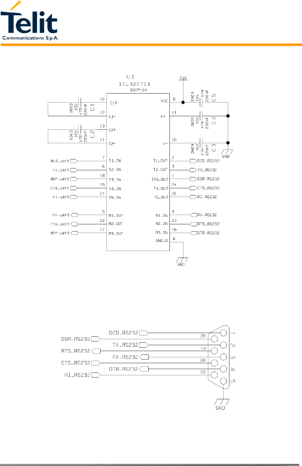
4.1 RS232 level translation
In order to interface the Telit GM862-QUAD with a PC com port or a RS232 (EIA/TIA-232)
application a level translator is required. This level translator must
- invert the electrical signal in both directions
- change the level from 0/3V to +15/-15V
Actually, the RS232 UART 16450, 16550, 16650 & 16750 chipsets accept signals with lower levels
on the RS232 side (EIA/TIA-562) , allowing for a lower voltage-multiplying ratio on the level
translator. Note that the negative signal voltage must be less than 0V and hence some sort of level
translation is always required.
The simplest way to translate the levels and invert the signal is by using a single chip level
translator. There are a multitude of them, differing in the number of driver and receiver and in the
levels (be sure to get a true RS232 level translator not a RS485 or other standards).
By convention the driver is the level translator from the 0-3V UART level to the RS232 level, while
the receiver is the translator from RS232 level to 0-3V UART.
In order to translate the whole set of control lines of the UART you will need:
- 5 driver
- 3 receiver
NOTE: The digital input lines working at 2.8VCMOS have an absolute maximum input voltage of 3,75V;
therefore the level translator IC shall not be powered by the +3.8V supply of the module. Instead it
shall be powered from a +2.8V / +3.0V (dedicated) power supply.
This is because in this way the level translator IC outputs on the module side (i.e. GM862-QUAD
inputs) will work at +3.8V interface levels, stressing the module inputs at its maximum input voltage.
This can be acceptable for evaluation purposes, but not on production devices.
Telit GM862-QUAD/-QUAD-PY
Hardware User Guide
1vv0300692, Rev. ISSUE#0, - 04/10/2005
Reproduction forbidden without DAI Telecom written authorization – All Right reserved – Right of modification reserved page 20 of 69
An example of level translation circuitry of this kind is:
the RS232 serial port lines are usually connected to a DB9 connector with the following layout:
Telit GM862-QUAD/-QUAD-PY
Hardware User Guide
1vv0300692, Rev. ISSUE#0, - 04/10/2005
Reproduction forbidden without DAI Telecom written authorization – All Right reserved – Right of modification reserved page 21 of 69
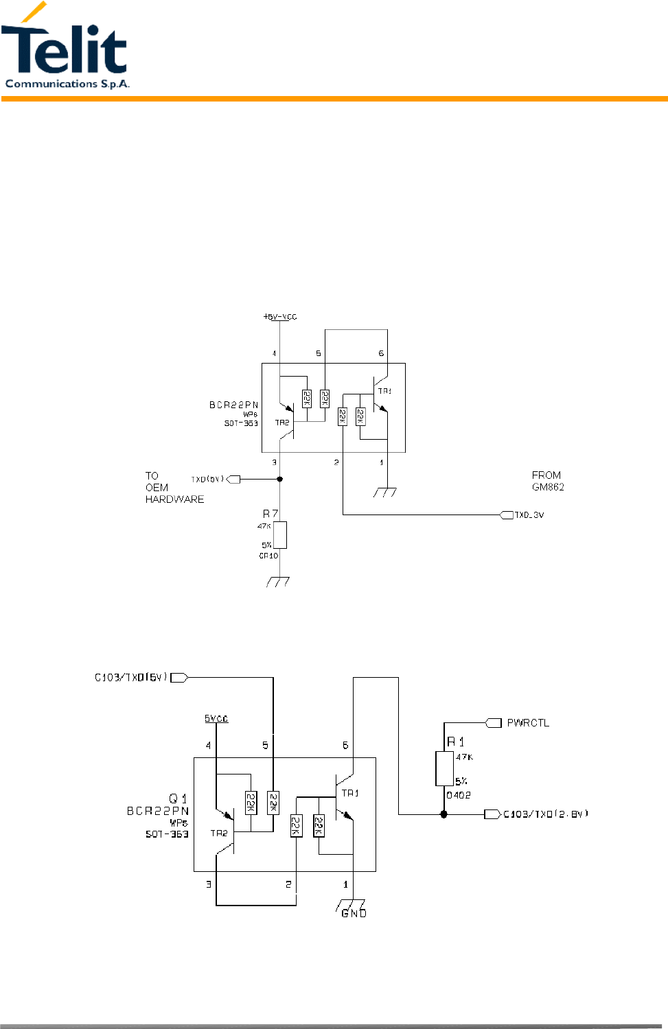
4.2 5V UART level translation
If the OEM application uses a microcontroller with a serial port (UART) that works at a voltage
different from 2.8 - 3V, then a circuitry has to be provided to adapt the different levels of the two
set of signals. As for the RS232 translation there are a multitude of single chip translators, but since
the translation requires very few components, then also a discrete design can be suited. For example
a possible inexpensive translator circuit for a 5V driver can be:
and for a 5V receiver:

Telit GM862-QUAD/-QUAD-PY
Hardware User Guide
1vv0300692, Rev. ISSUE#0, - 04/10/2005
Reproduction forbidden without DAI Telecom written authorization – All Right reserved – Right of modification reserved page 22 of 69
NOTE: The UART input line TXD (rx_uart) of the GM862-QUAD is NOT internally pulled up with a
resistor, so there may be the need to place an external 47KΩ pull-up resistor, either the DTR (dtr_uart)
and RTS (rts_uart) input lines are not pulled up internally, so an external pull-up resistor of 47KΩ may
be required.
A power source of the internal interface voltage corresponding to the 2.8VCMOS high level is
available at the PWRCTL pin on the connector, whose absolute maximum output current is 10mA.
A maximum of 9 47 KΩ pull-up resistors can be connected to the PWRCTL pin, provided no other
devices are connected to it and the pulled-up lines are GM862-QUAD input lines connected to
open collector outputs in order to avoid latch-up problems on the GM862-QUAD.
Care must be taken to avoid latch-up on the GM862-QUAD and the use of this output line to power
electronic devices shall be avoided, especially for devices that generate spikes and noise such as
level translators, digital ICs or microcontrollers, failure in any of these condition can severely
compromise the GM862-QUAD functionality.
NOTE: The input lines working at 2.8VCMOS can be pulled-up with 47KΩ resistors that can be
connected directly to the PWRCTL line provided they are connected as in this example.
NO OTHER devices should be powered with the PWRCTL line, otherwise the module functionality may
be compromised.

Telit GM862-QUAD/-QUAD-PY
Hardware User Guide
1vv0300692, Rev. ISSUE#0, - 04/10/2005
Reproduction forbidden without DAI Telecom written authorization – All Right reserved – Right of modification reserved page 23 of 69
5 Microphone
The microphone circuitry is the more noise sensitive and its design and layout must be done with
particular care.
5.1 Microphone line Characteristic and
requirements
The Telit GM862-QUAD provides two audio paths for the microphone and the earpiece: the
internal and the external audio paths. Only one of the two paths can be active at a time and it is
selectable by hardware line AXE or by AT command. The audio characteristics of the two paths are
slightly different and this should be kept in mind when designing. The internal audio path should be
used for handset function, while the external audio path is suited for hands free function (car kit).
Both microphone paths from the Telit GM862-QUAD are balanced and the OEM circuitry should
be designed balanced to reduce the common mode noise typically generated on the ground plane,
however for particular OEM application needs also an unbalanced circuitry can be used.
The microphone input lines characteristics are:
internal microphone path
• line coupling: AC ( 100nF cond.)
• line type: balanced
• differential input resistance: 25kΩ
• line nominal sensitivity: 50 mVrms
• max input voltage: 360 mVrms
• microphone nominal sensitivity/analog gain suggested: -45 dBVrms/Pa / +24dB
• echo canceller type: handset
external microphone path
• line coupling: AC ( 100nF cond.)
• line type: balanced
• differential input resistance: 25kΩ
• line nominal sensitivity: 3 mVrms
• max input voltage: 22 mVrms
• microphone nominal sensitivity/analog gain suggested: -45 dBVrms/Pa / +10dB
• echo canceller type: car kit hands free

Telit GM862-QUAD/-QUAD-PY
Hardware User Guide
1vv0300692, Rev. ISSUE#0, - 04/10/2005
Reproduction forbidden without DAI Telecom written authorization – All Right reserved – Right of modification reserved page 24 of 69
TIP: Due to the difference in the echo canceller type, the internal audio path is suited for handset
applications while the external audio path is suited for car kit hands free. The headset applications
should be made by using the external audio path but DISABLING the echo canceller by software AT
command. If the echo canceller is left active with the headset, then some echo might be introduced by
the echo cancel algorithm.
The nominal sensitivity of the line indicates the voltage level on the GM862-QUAD pins that
should be present during "normal spoken" conditions: for a handset a voice signal coming from the
mouth of the talker at 7 cm of distance from the microphone, producing an acoustic pressure of -4,7
dBPa (@ 1 kHz) on the microphone membrane.
For example:
With the internal mic. having the suggested nominal sensitivity -45dBVrms/Pa
at the "normal spoken" conditions: -4.7dB Pa on the microphone membrane.
At that acoustic pressure the voltage output from the microphone is:
Voltage Output (dB) = ( -45) + (-4.7) = -49.7 dBVrms
corresponding to:
Voltage Output = 10 ( -49.7 / 20 ) = 3.3* 10 -3 Vrms
by having the microphone gain set to +24 dB (corresponding to 15.8 times) the signal in the
nominal conditions on the input mic. pins of the GM862-QUAD will be:
Voltage @ GM862-QUAD_mic = 3.3 * 10 -3 * 15.8 = 51 mVrms
During the spoken conditions the signal varies according to the volume of the voice of the talker,
usually a rough thumb rule for the dynamic range may be considered:
* +20dB (10 times) at maximum voice level (talker screaming)
* -50 dB (1/300 times) at minimum voice level (talker whispering).
For the handsfree/car kit microphone the voice attenuation due to the distance between the
microphone and the talker must be taken into account when designing the microphone amplifier.
For a car cabin usually the distance between the talker and the mic. is about 50cm; in these
conditions the attenuation can be considered as a thumb rule around 20dB.
Another thing to consider, especially for cabin car use, is the fact that the external mic. will pick up
also ambient noise; to overcome this problem it is preferable to set the gain of the microphone 10dB
lower with respect to the calculated value for a nominal sensitivity. The corresponding reduction in
signal level will be compensated by an increased voice volume of the talker which will speak louder
because of the ambient noise.

Telit GM862-QUAD/-QUAD-PY
Hardware User Guide
1vv0300692, Rev. ISSUE#0, - 04/10/2005
Reproduction forbidden without DAI Telecom written authorization – All Right reserved – Right of modification reserved page 25 of 69
For the headset we shall distinguish two different types: the headsets having the microphone
sustained close to the mouth and the headsets having the microphone on the earpiece cable.
The same considerations for the additional voice attenuation due to the distance from the
microphone and the noise pick up can be made for the headset having the microphone on the
earpiece cable, while the other kind of headset shall be threaten as an handset.
For example:
With the external mic. having the suggested nominal sensitivity -45dBVrms/Pa
at the "normal spoken" conditions: -4.7dB Pa at 7 cm from the mouth of the talker and with a
further attenuation of 20dB due to the distance from the microphone (about 50 cm).
At that acoustic pressure the voltage output from the microphone is:
Voltage Output (dB) = ( -45) + (-4.7) - 20 = -69.7 dBVrms
corresponding to:
Voltage Output = 10 ( -69.7 / 20 ) = 3.3* 10 -4 Vrms
by having the microphone gain set to +10 dB (corresponding to 3 times) the signal in the nominal
conditions on the input external mic. pins of the GM862-QUAD will be:
Voltage @ GM862-QUAD__extmic = 3.3 * 10 -4 * 3 = 1 mVrms
Hence in these conditions the signal level on the input pins of the external mic. of the GM862-
QUAD is 10 dB (3 times) lower than the nominal, as suggested.
The microphones usually need a biasing network that provides the necessary DC current to the mic.,
this will be explained further on.
In the EVK all the microphone input jacks have the hot wire connected to the central pole.

Telit GM862-QUAD/-QUAD-PY
Hardware User Guide
1vv0300692, Rev. ISSUE#0, - 04/10/2005
Reproduction forbidden without DAI Telecom written authorization – All Right reserved – Right of modification reserved page 26 of 69
5.2 General Design Rules
There are several configurations for the audio path, but the most effective difference is between
balanced and unbalanced microphone.
It is highly recommended to keep the whole microphone path balanced even if this means having 2
wires connecting the microphone instead of one needed (plus ground) in the unbalanced case. The
balanced circuitry is more suited because of its good common mode noise rejection, reducing the
216 Hz burst noise produced during the GSM transmissions.
• Where possible use balanced microphone circuitry
• Keep the microphone traces on the PCB and wires as short as possible.
• If your application requires an unbalanced microphone, then keep the lines on the PCB
balanced and "unbalance" the path close to the microphone wire connector if possible.
• For the microphone biasing voltage use a dedicated voltage regulator and a capacitor multiply
circuit.
• Make sure that the microphone traces in the PCB don't cross or run parallel to noisy traces
(especially the power line)
• If possible put all around to the microphone lines a ground trace connected to the ground plane
by several vias. This is done in order to simulate a shielded trace on the PCB.
• The biasing circuit and eventually the buffer can be designed in the same manner for the
internal and external microphones.
5.3 Microphone Biasing
The electret microphones usually need a biasing voltage to work properly. Refer to your
microphone provider for the characteristics required.
NOTE: The microphones have a hot wire were the positive biasing must be connected, usually it is
indicated by a + sign or a red point. If the polarity of the bias is reversed, then the microphone will not
work properly. For this reason be sure to respect the mic. biasing polarity.
Telit GM862-QUAD/-QUAD-PY
Hardware User Guide
1vv0300692, Rev. ISSUE#0, - 04/10/2005
Reproduction forbidden without DAI Telecom written authorization – All Right reserved – Right of modification reserved page 27 of 69
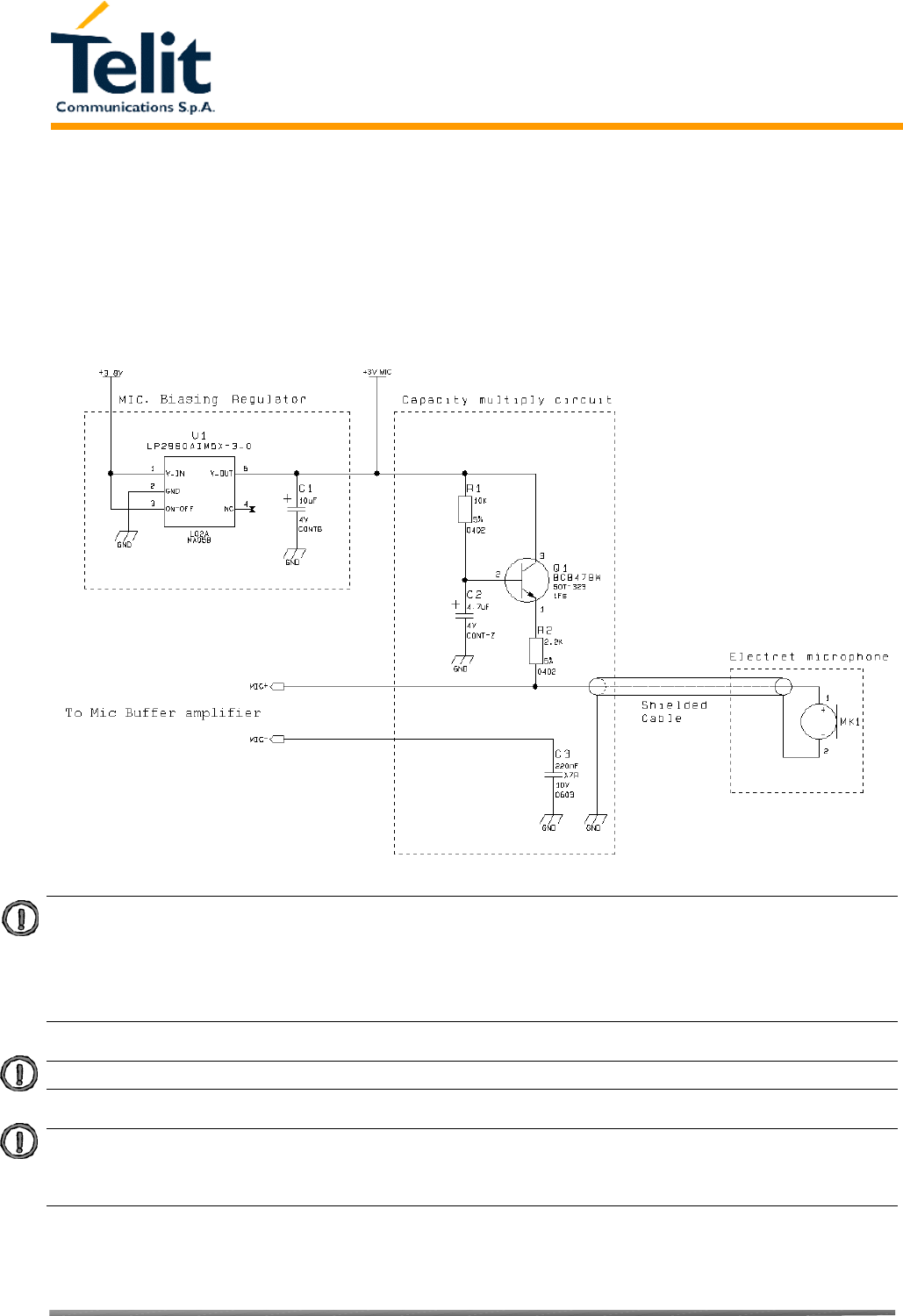
5.3.1 Balanced Microphone biasing
The balanced microphone bias voltage should be obtained from a dedicated voltage regulator, in
order to eliminate the noise present on the power lines. This regulator can be the same for all the
audio paths. The microphone should be supplied from a capacitor multiply circuit.
For example a circuit for the balanced microphone biasing can be:
NOTE: In the balanced application the resistors R2 and R3 must have the same value to keep the
circuit balanced.
NOTE: The cable to the microphone should not be shielded, instead a twisted pair cable shall be used.
NOTE: The microphone sensitivity changes with the value of R2 and R3. Usually the microphones are
characterized with 2kΩ biasing resistance, so try to keep the sum of R2 and R3 around 2kΩ. Refer to
your microphone manufacturer for the mic. characteristics.
Telit GM862-QUAD/-QUAD-PY
Hardware User Guide
1vv0300692, Rev. ISSUE#0, - 04/10/2005
Reproduction forbidden without DAI Telecom written authorization – All Right reserved – Right of modification reserved page 28 of 69
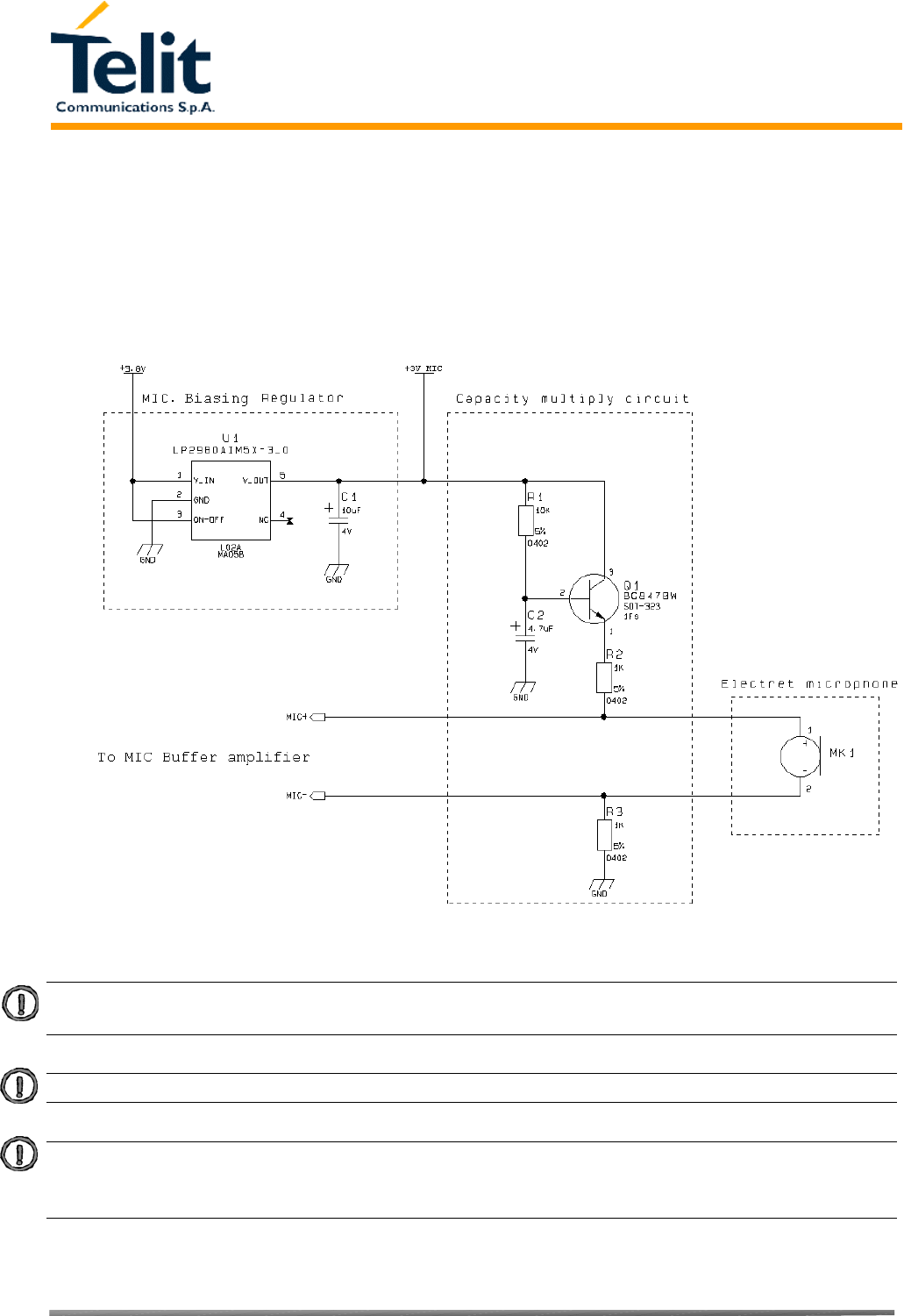
5.3.2 Unbalanced Microphone biasing
The unbalanced microphone biasing voltage should be obtained from a dedicated voltage regulator,
in order to eliminate the noise present on the power lines. This regulator can be the same for all the
audio paths. The microphone should be supplied from a capacitor multiply circuit.
For example a circuit for the unbalanced microphone biasing can be:
NOTE: In the unbalanced application the capacitor C3 shall be > 200nF otherwise the frequency
response will be cut at low band frequencies (down to 300Hz). This capacitor can be placed close to
the MIC- pin (EXT_MIC- or INT_MIC- depending on the audio path chosen) or if possible it should be
placed close to the shielded cable connector. If the ground return path is well designed, then it is
possible to eliminate the C3 capacitor, provided the buffer is close to the mic. input.
NOTE: The cable to the microphone should be shielded.
NOTE: The microphone sensitivity changes with the value of R2. Usually the microphones are
characterized with 2kΩ biasing resistance, so try to keep the value of R2 around 2kΩ. For mic.
characteristics refer to the manufacturer.
Telit GM862-QUAD/-QUAD-PY
Hardware User Guide
1vv0300692, Rev. ISSUE#0, - 04/10/2005
Reproduction forbidden without DAI Telecom written authorization – All Right reserved – Right of modification reserved page 29 of 69
5.4 Microphone buffering
As seen previously, a microphone shall be connected to the input pins of the GM862-QUAD
through a buffer amplifier that boosts the signal level to the required value.
Again the buffered microphone circuitry can be balanced or unbalanced. Where possible it is
always preferable a balanced mic. solution. The buffering circuit shall be placed close to the
microphone or close to the microphone wire connector.
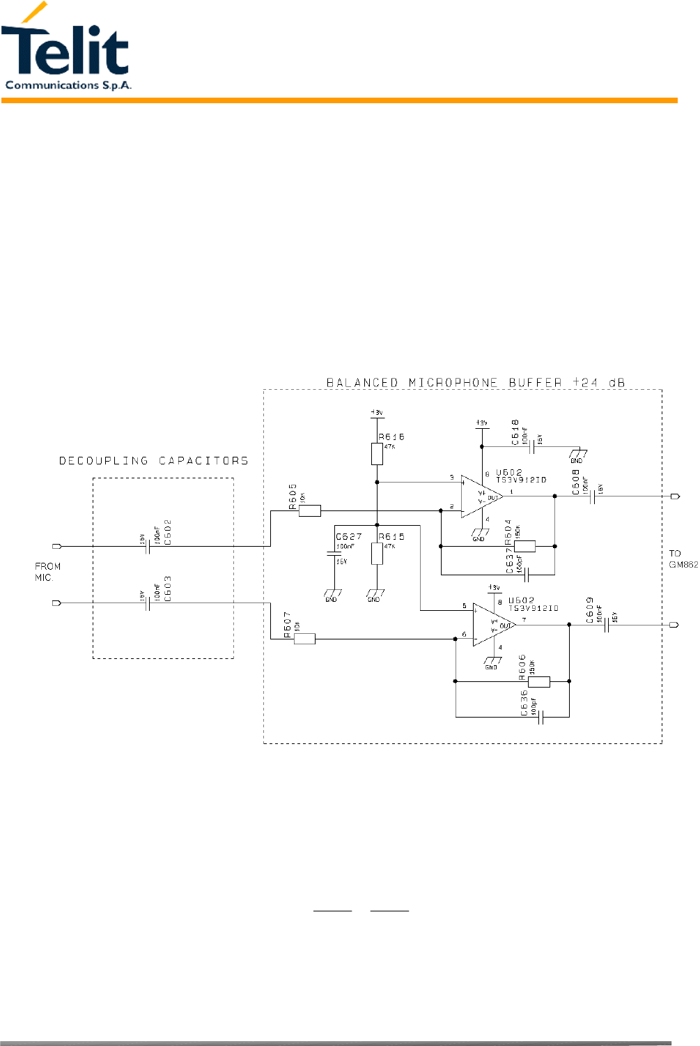
5.4.1 Buffered Balanced Mic.
A sample circuit can be:
This circuit has a gain of 15 times (+24 dB), and is therefore suited for the internal mic. input,
having a microphone with a sensitivity close to the suggested one (-45 dBVrms/Pa), if the used
microphone has a different sensitivity, or if the buffer is connected to the external mic. input, then a
gain adjustment shall be done by changing resistors R604-R605 and R606-R607 and as a
consequence the capacitors C636 and C637 to maintain the bandwidth 150-8000 (-3dB).
The buffer gain is given by the formula:
607
606
605
604
R
R
R
R
Gain ==
The C636 and C637 capacitors are placed in order to cut off the gain at higher frequencies than the
transmitted GSM band, the cutoff frequency (-3dB) should be 8 kHz in order to have -1dB at 4Khz.
The cutoff frequency is given by the formula:

Telit GM862-QUAD/-QUAD-PY
Hardware User Guide
1vv0300692, Rev. ISSUE#0, - 04/10/2005
Reproduction forbidden without DAI Telecom written authorization – All Right reserved – Right of modification reserved page 30 of 69
636*606*2
1
637*604*2
1
.CRCR
freq
ππ
== [Hz]
For example:
- Let's assume you have a microphone with these characteristics:
- sensitivity -45 dBVrms/Pa
and you want to use it in the internal mic. audio path.
With the mic. having nominal sensitivity -45dBVrms/Pa at the "normal spoken" conditions: -4.7dB Pa
at 7 cm from the mouth of the talker.
At that acoustic pressure the voltage output from the microphone is:
Mic Voltage Output (dB) = ( -45) + (-4.7) = -49.7 dBVrms
corresponding to:
Mic_Voltage_Output = 10 ( -49.7 / 20 ) = 3.3* 10 -3 Vrms
in order to have a signal of 50 mVrms on the GM862-QUAD internal mic. inputs then the buffer must
have a gain of:
Voltage @ GM862-QUAD_intmic/ Mic_Voltage_Output = (50 * 10 -3 )/( 3.3 * 10 -3 ) = 15
Hence in these conditions the signal level on the input pins of the internal mic. of the GM862-
QUAD is 24 dB (15 times) higher than the microphone output and therefore the buffer has to gain
24 dB.
The corresponding values for the resistors on the buffer could be ( if we keep the input resistance
10kΩ )
R604 = R606 = gain* R603= gain* R605 = 15* 10 = 150 kΩ
The commercial values of 150kΩ & 10kΩ are then chosen.
As a consequence the values of the capacitors C636 and C637 shall be:
C636=C637= 1/ (2π*8000*R606)= 132 *10 -12 F
A commercial value of 100pF is then chosen.
Telit GM862-QUAD/-QUAD-PY
Hardware User Guide
1vv0300692, Rev. ISSUE#0, - 04/10/2005
Reproduction forbidden without DAI Telecom written authorization – All Right reserved – Right of modification reserved page 31 of 69
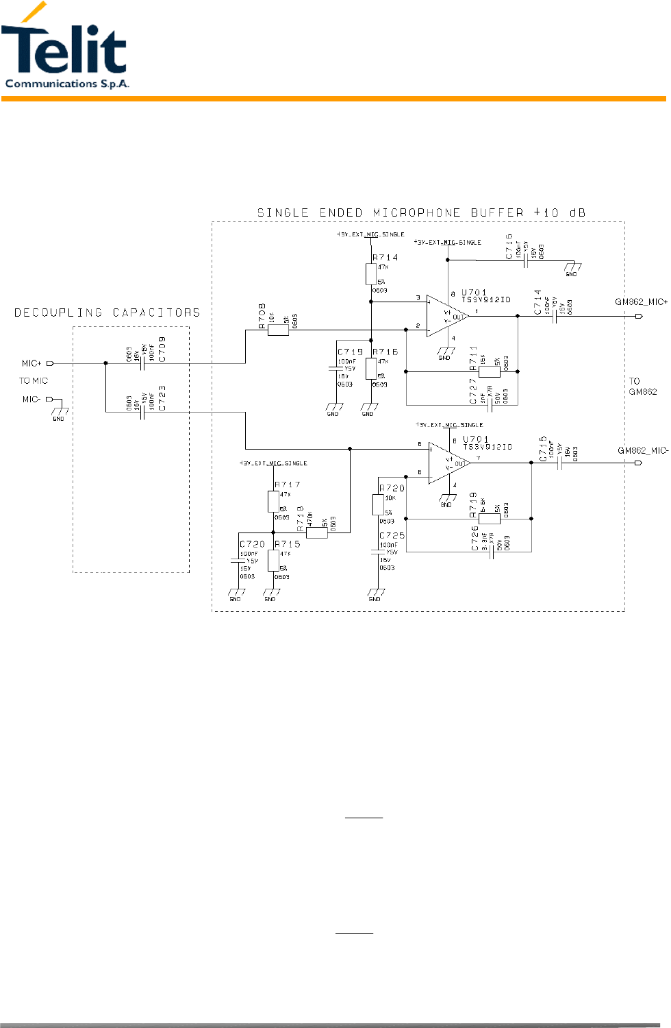
5.4.2 Buffered Unbalanced (Single Ended) Mic.
A sample schematic for a buffered unbalanced (single ended) microphone can be:
The schematic does not include the required mic. biasing circuitry. For the biasing the same circuit
as seen before can be used; to be noticed that the capacitor C3 on the unbalanced biasing circuit is
not anymore needed if this Buffered design is used.
Two different configurations are used, one inverting and the other not inverting, hence an additional
+6dB (2 times) gain is achieved by doubling the mic. signal path.
The gain of the not inverting buffer is given by the formula:
720
719
1R
R
Gain +=
and hence it cannot be less than 1. In the example shown the gain of the not inverting buffer is 1,5
(4dB).
While the gain of the inverting buffer is given by the formula:
708
711
R
R
Gain =
As shown in the balanced buffered mic. the gain adjustments can be done by changing R719 - R720
and R708 - R711 and as a consequence the capacitors C726 and C727.

Telit GM862-QUAD/-QUAD-PY
Hardware User Guide
1vv0300692, Rev. ISSUE#0, - 04/10/2005
Reproduction forbidden without DAI Telecom written authorization – All Right reserved – Right of modification reserved page 32 of 69
The bandwidth (-3dB) is given by the approximated formula (considering C725 >> C726) :
727*711*2
1
726*719*2
1
.CRCR
freq
ππ
== [Hz]
The buffer bandwidth at -3dB shall be 8kHz.
Note that the biasing of the operational amplifier is given for the inverting amplifier by the series
divider R714-R715. The 100nF capacitor C719 is needed to filter the noise that could be coupled to
that divider. For the not inverting operational the biasing is given by a different divider R715-R717
with the capacitor C720 and through a series resistor R718 of 470KΩ.
For example:
- Let's assume you have a microphone with these characteristics:
- sensitivity -45 dBVrms/Pa
and you want to use it in the external mic. audio path.
With the mic. having nominal sensitivity -45dBVrms/Pa at the "normal spoken" conditions: -4.7dB Pa
but at 50 cm from the mouth of the talker an additional 20 dB loss shall be considered.
At that acoustic pressure the voltage output from the microphone is:
Mic Voltage Output (dB) = ( -45) + (-4.7) -20 = -69.7 dBVrms
corresponding to:
Mic_Voltage_Output = 10 ( -69.7 / 20 ) = 3.3* 10 -4 Vrms
in order to have a signal of 1 mVrms (10 dB lower than the nominal input for the GM862-QUAD
external mic. path) on the GM862-QUAD internal mic. inputs then the buffer must have a gain of:
Voltage @ GM862-QUAD_intmic/ Mic_Voltage_Output = (1 * 10 -3 )/( 3.3 * 10 -4 ) = 3
Hence in these conditions the signal level on the input pins of the internal mic. of the GM862-
QUAD is 10 dB (3 times) higher than the microphone output and therefore the buffer has to gain 10
dB.
To calculate the resistor values it must be kept in mind that balancing the line will double the signal
and hence already add +6 dB, therefore the buffer must gain only 1.5 times.
The corresponding values for the resistors on the buffer could be ( if we keep the input resistance
10kΩ )
R711 = gain* R708= 1.5* 10 = 15 kΩ
R719 = (gain -1) * R720 = (1.5 -1) * 10 = 5 kΩ
The commercial values of 15kΩ & 5.6kΩ are then chosen.

Telit GM862-QUAD/-QUAD-PY
Hardware User Guide
1vv0300692, Rev. ISSUE#0, - 04/10/2005
Reproduction forbidden without DAI Telecom written authorization – All Right reserved – Right of modification reserved page 33 of 69
As a consequence the values of the capacitors C726 and C727 shall be:
C726= 1/ (2π*8000*R719)= 3.5 *10 -9 F
C727= 1/ (2π*8000*R711)= 1,2 *10 -9 F
The commercial values of 3.3nF and 1nF are then chosen.

Telit GM862-QUAD/-QUAD-PY
Hardware User Guide
1vv0300692, Rev. ISSUE#0, - 04/10/2005
Reproduction forbidden without DAI Telecom written authorization – All Right reserved – Right of modification reserved page 34 of 69
6 Speaker
6.1 Speaker lines characteristics and requirements
The Telit GM862-QUAD provides two audio paths for both the microphone and the earpiece: the
internal and the external audio paths. Only one of the two paths can be active at a time and it is
selectable by hardware line AXE or by AT command. The audio characteristics of the two paths are
slightly different and this should be kept in mind when designing your application. The internal
audio path should be used for handset function, while the external audio path is suited for hands free
function (car kit).
Both speaker outputs from the Telit GM862-QUAD are bridged type and the OEM circuitry shall
be designed bridged to reduce the common mode noise typically generated on the ground plane and
to get the maximum power output from the device; however for particular OEM application needs
also a single ended circuitry can be designed.
The GM862-QUAD speaker output lines characteristics are:
internal speaker path ( EAR_MT+ , EAR_MT- )
• line coupling: DC
• line type: bridged
• speaker impedance (operating conditions): ≥ 16 Ω ± 5% @ 1kHz
• minimum load impedance: 15 Ω
• signal bandwidth: 150 - 8000 Hz @ -3 dB
• maximum differential output: 850 mVrms
• rated output power: 10 mW
• maximum power output: 30 mW
• volume level steps (SW): - 2 dB
• number of volume steps(SW): 10
external speaker path ( EAR_HF+ , EAR_HF- )
• line coupling: DC
• line type: bridged
• speaker impedance (operating conditions): ≥ 16 Ω ± 15% @ 1kHz
• minimum load impedance: 15 Ω
• signal bandwidth: 150 - 8000 Hz @ -3 dB
• maximum differential output: 425 mVrms
• rated output power: 2.5 mW

Telit GM862-QUAD/-QUAD-PY
Hardware User Guide
1vv0300692, Rev. ISSUE#0, - 04/10/2005
Reproduction forbidden without DAI Telecom written authorization – All Right reserved – Right of modification reserved page 35 of 69
• maximum power output: 7.5 mW
• volume level steps (SW): - 2 dB
• number of volume steps (SW): 10
The EVK v.1.2 audio output characteristics are:
internal/external ear single ended
• line coupling: AC
• line type: single ended referred to GND
• speaker impedance (operating conditions): ≥ 8 Ω
• minimum load impedance: 8 Ω
• signal bandwidth: 150 - 8000 Hz @ -3 dB
• maximum output: 800 mVrms
• maximum power output: 80 mW @ 8 Ω
• THD+N 1% @ 80mW
internal/external ear bridged
• line coupling: DC
• line type: bridged not referred to GND
• speaker impedance (operating conditions): ≥ 8 Ω
• minimum load impedance: 8 Ω
• signal bandwidth: 150 - 8000 Hz @ -3 dB
• maximum output: 1.6 Vrms
• maximum power output: 320 mW @ 8 Ω
• THD+N 1% @ 330mW
high power external ear
• line coupling: DC
• line type: bridged not referred to GND
• speaker impedance (operating conditions): ≥ 4 Ω
• minimum load impedance: 4 Ω
• signal bandwidth: 150 - 8000 Hz @ -3 dB
• maximum power output: 6 W
• THD+N 10% @ 6 W

Telit GM862-QUAD/-QUAD-PY
Hardware User Guide
1vv0300692, Rev. ISSUE#0, - 04/10/2005
Reproduction forbidden without DAI Telecom written authorization – All Right reserved – Right of modification reserved page 36 of 69
6.2 General Design rules
There are several configurations for the audio output path, but the various design requirements can
be grouped into three different categories:
• handset earphone (low power, typically a handset)
• hands free earphone (low power, typically a headset)
• car kit speakerphone (high power, typically a speaker)
The three groups have different power requirements, usually the first two applications need only
few mW of power, which can be directly drained from the GM862-QUAD pins, provided a suited
speaker is used. This direct connect design is the cheaper and simpler solution and will be suited for
the most of the earphone design requirements. There's no need to decouple the output ear lines if a
suited earpiece is connected. For the last group, the speakerphone, a power amplifier is required to
raise the output power up to 5-10W required in a car cabin application.
All the designs shall comply with the following guidelines:
• Where possible use a bridged earphone circuitry, to achieve the maximum power output from
the device.
• Keep the earphone traces on the PCB and wires as short as possible.
• If your application requires a single ended earpiece and you want a direct connection, then
leave one of the two output lines open and use only the other referred to ground. Remember
that in this case the power output is 4 times lower than the bridged circuit and may not be
enough to ensure a good voice volume.
• Make sure that the earphone traces in the PCB don't cross or run parallel to noisy traces
(especially the power line)
• The cable to the speaker shall be a twisted pair with both the lines floating for the bridged
output type, shielded with the shield to ground for the single ended output type.
6.2.1 Noise Filtering
The I/O of the PCB should have a noise filter close to the connector, to filter the high frequency
GSM noise. The filter can be a Π of 2 capacitor and a inductance, with the one capacitor of 39pF -
0603 case , and the other capacitor of 1nF - 0603; the inductance shall have a value of 39μH .
6.3 Handset earphone design
As seen previously, a 16Ω speaker can be directly connected to the output pins EAR_MT+ and
EAR_MT- of the GM862-QUAD.
This solution is often the more cost effective, reducing the components count to a minimum. There
are several limitations to the use of this solution: speaker direct connect imposes the speaker
characteristics to be almost exactly the suggested ones, otherwise the power output may be reduced
Telit GM862-QUAD/-QUAD-PY
Hardware User Guide
1vv0300692, Rev. ISSUE#0, - 04/10/2005
Reproduction forbidden without DAI Telecom written authorization – All Right reserved – Right of modification reserved page 37 of 69
(if speaker impedance is bigger than 16Ω) or the GM862-QUAD ear port may be damaged (if
speaker impedance is less than 15Ω).
The other limitation of the speaker direct connection is the power output capability of the GM862-
QUAD which is limited and for some particular applications may not be enough.
For these reasons, when the power output of the GM862-QUAD is not enough or if the speaker
characteristics are different from the suggested, then it is preferable to use an amplifier to increase
the power and current output capabilities.
Again the output from the GM862-QUAD is bridged and both lines should be used, where possible,
as inputs to the power amplifier. This ensures a higher common mode rejection ratio, reducing the
GSM current busts noise on the speaker output.
In this case the EAR_MT lines from the GM862-QUAD should be AC coupled with a capacitor of
100nF.
It is always desirable to have a mute control on the amplifier, in order to turn it off while the device
is not sending signal to the output, in this manner the amplifier background noise which may be
audible during idle conditions is cut off.
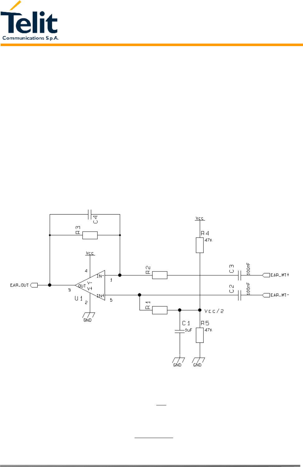
A principle schematic may be:
The resulting gain and high pass cut can be obtained with the formula:
2
3
R
R
Gain =
4*3*2
1
.CR
freq
π
= [Hz]
Telit GM862-QUAD/-QUAD-PY
Hardware User Guide
1vv0300692, Rev. ISSUE#0, - 04/10/2005
Reproduction forbidden without DAI Telecom written authorization – All Right reserved – Right of modification reserved page 38 of 69
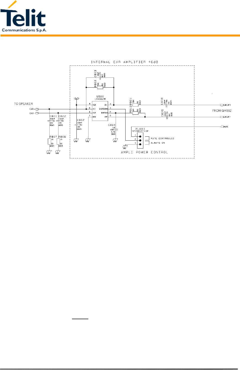
And an example of internal Ear amplifier is:
Some amplifier require a low impedance load at high frequency in order to avoid auto oscillation,
this can be made with a capacitor (100nF) in series with a resistor (15Ω).
When designing your application, remember to provide an adequate bypass capacitor to the
amplifier and place it close to the power input pin of the IC, keeping the traces as short as possible.
6.4 Hands Free earphone (low power) design
The same design considerations made for the handset are valid for the hands free earphone, the only
difference is that the external ear audio output level from the GM862-QUAD is 6dB lower than the
internal one, so the gain of the amplifier must be 6dB higher to provide the same audio level.
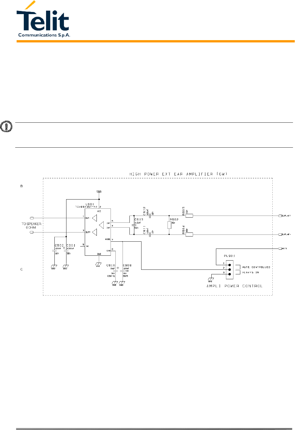
6.5 Car Kit speakerphone design
For the car kit speaker phone function the power output requirement is usually at least 4W,
therefore an amplifier is needed to boost the GM862-QUAD output.
The design of the amplifier shall comply with the following guidelines:
• The input to the amplifier MUST be taken from the external audio path (EAR_HF+, EAR_HF-)
of the GM862-QUAD, because of its echo canceller parameters suited to a car cabin use.
• The amplifier shall have a gain of 30-40 times ( 29-32 dB) to provide the desired output power
of 5-10W with the signal from the GM862-QUAD external audio output lines (EAR_HF).
• If the amplifier has a fixed gain then it can be adjusted to the desired value by reducing the input
signal with a resistor divider network.
Telit GM862-QUAD/-QUAD-PY
Hardware User Guide
1vv0300692, Rev. ISSUE#0, - 04/10/2005
Reproduction forbidden without DAI Telecom written authorization – All Right reserved – Right of modification reserved page 39 of 69
• The amplifier shall have a mute control to be used while not in conversation. This results in two
benefits: eliminating the background noise when not in conversation and saving power.
• The power to the amplifier should be decoupled as much as possible from the GM862-QUAD
power supply, by either keeping separate wires and placing bypass capacitors of adequate value
close to the amplifier power input pins.
• The biasing voltage of the amplifier shall be stabilised with a low ESR (e.g. a tantalum)
capacitor of adequate value.
NOTE: The GM862-QUAD audio path connected to the car kit hands free amplifier MUST be the
external one (EAR_HF), otherwise the echo cancellation will not be done due to the difference in the
echo canceller characteristics of the GM862-QUAD internal audio path from the external audio path.
An example of car kit amplifier schematic can be:

Telit GM862-QUAD/-QUAD-PY
Hardware User Guide
1vv0300692, Rev. ISSUE#0, - 04/10/2005
Reproduction forbidden without DAI Telecom written authorization – All Right reserved – Right of modification reserved page 40 of 69
7 General Purpose I/O
The general purpose I/O pins can be configured to act in three different ways:
- input
- output
- alternate function (internally controlled)
Input pins can only be read and report the digital value (high or low) present on the pin at the read
time; output pins can only be written or queried and set the value of the pin output; an alternate
function pin is internally controlled by the GM862-QUAD firmware and acts depending on the
function implemented.
Not all GPIO pins support all these three modes:
- GPIO1 is an INPUT ONLY
- GPIO2 is an OUTPUT ONLY (open collector)
- GPIO3, GPIO4 and GPIO5 support both input or output mode but not Alternate function.
- GPIO6 supports all three modes and can be input, output, alarm output (Alternate function)
- GPIO7 supports all three modes and can be input, output, buzzer output (Alternate function)
All GPIO pins except from GPIO1 and GPIO2 that are buffered with a transistor, are 2.8V CMOS
signals and their interface levels are the same specified in the paragraph 4 Serial Port.
7.1 Using a GPIO pin as INPUT
The GPIO pins, when used as inputs, can be connected to a digital output of another device and
report its status, provided this device has interface levels compatible with the 2.8V CMOS levels of
the GPIO.
If the digital output of the device to be connected with the GPIO input pin has interface levels
different from the 2.8V CMOS, then it can be connected to GPIO1 or can be buffered with an open
collector transistor, provided a 47KΩ pull-up resistor is connected as seen in the paragraph 4.2 5V
UART level translation.
7.2 Using a GPIO pin as OUTPUT
The GPIO pins, when used as outputs, can drive 2.8V CMOS digital devices or compatible
hardware. When set as outputs, the pins (except from GPIO2 which is Open Collector) have a push-
pull output and therefore the pull-up resistor may be omitted.
The GPIO2 pin, since it is an Open Collector output needs an external pull-up resistor.
Telit GM862-QUAD/-QUAD-PY
Hardware User Guide
1vv0300692, Rev. ISSUE#0, - 04/10/2005
Reproduction forbidden without DAI Telecom written authorization – All Right reserved – Right of modification reserved page 41 of 69
7.3 Using the Alarm Output GPIO6
The GPIO6 pin, when configured as Alarm Output, is controlled by the GM862-QUAD module and
will rise when the alarm starts and fall after the issue of a dedicated AT command.
This output can be used to power up the GM862-QUAD controlling microcontroller or application
at the alarm time, giving you the possibility to program a timely system wake-up to achieve some
periodic actions and completely turn off either the application and the GM862-QUAD during sleep
periods, drammatically reducing the sleep comsumption to few μA.
In battery powered devices this feature will greatly improve the autonomy of the device.
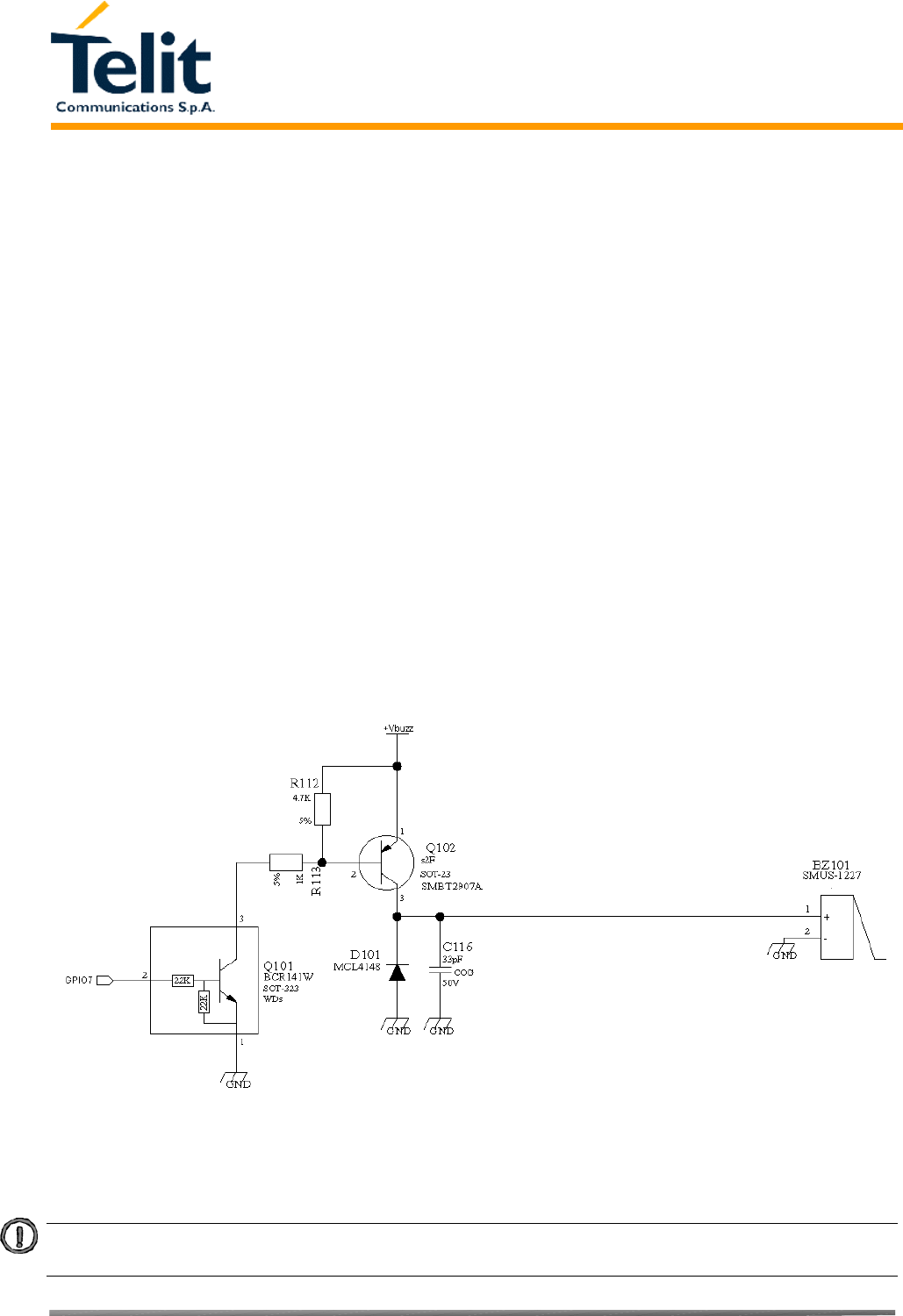
7.4 Using the Buzzer Output GPIO7
The GPIO7 pin, when configured as Buzzer Output, is controlled by the GM862-QUAD module
and will drive with appropriate square waves a Buzzer driver.
This permits to your application to easily implement Buzzer feature with ringing tones or melody
played at the call incoming, tone playing on SMS incoming or simply playing a tone or melody
when needed by your application.
A sample interface scheme is included below to give you an idea of how to interface a Buzzer to the
GPIO7:
NOTE: To correctly drive a buzzer a driver must be provided, its characteristics depend on the Buzzer
and for them refer to your buzzer vendor.
Telit GM862-QUAD/-QUAD-PY
Hardware User Guide
1vv0300692, Rev. ISSUE#0, - 04/10/2005
Reproduction forbidden without DAI Telecom written authorization – All Right reserved – Right of modification reserved page 42 of 69
8 Camera
8.1 Agilent Camera
The GM862-QUAD provides a direct support for digital cameras with the following characteristics:
Type: AGILENT ADCM2650
Technology: CMOS COLOR camera
Max picture size: VGA 640x480 pixels
Output format: JPEG
Sensitivity: 5 lux
8.1.1 Camera interface connectors
The interface connection between GM862-QUAD and camera is provided by the 50-pins Molex
connector of the module and a 18-pins ZIF connector vertical type for the CMOS camera.
Molex 52991-0508 GM862 ZIF CF21181V0RP
Pin Signal I/O Function Pin Signal I/O
21 CAM_SYNC I End of frame is an output for the
camera and an input for the GM862-
QUAD.
16 EOF O
25 MON1_CAM O The module clock is provided by the
MON1_CAM output of the GM862-
QUAD.
17 MCLK I
28 IICSCL_CAM O IICbus serial clock 4 S_CLK I
32 PD(0) I/O Parallel Data 0 15 DATA0 I/O
34 PD(1) I/O Parallel Data 1 14 DATA1 I/O
38 PD(2) I/O Parallel Data 2 13 DATA2 I/O
40 PD(3) I/O Parallel Data 3 12 DATA3 I/O
42 PD(4) I/O Parallel Data 4 11 DATA4 I/O
44 PD(5) I/O Parallel Data 5 10 DATA5 I/O
46 PD(6) I/O Parallel Data 6 9 DATA6 I/O
49 PD(7) I/O Parallel Data 7 8 DATA7 I/O
47 IICSDA_CAM I/O IICbus serial data 3 S_DATA I/O
Telit GM862-QUAD/-QUAD-PY
Hardware User Guide
1vv0300692, Rev. ISSUE#0, - 04/10/2005
Reproduction forbidden without DAI Telecom written authorization – All Right reserved – Right of modification reserved page 43 of 69
48 CAM_DRDY I Data ready in an output for the camera
and an input for the GM862-QUAD
7 DR O
50 CAM_PWR_ON O 2,8V power supply enable for the
camera
2 VCC_MAIN I
Horizontal sync n.c. 6 HSYNC O
Input command for switching power
ON or OFF
5 ON_OFF I
2-4-
6
GND Ground 1-
18
GND

Telit GM862-QUAD/-QUAD-PY
Hardware User Guide
1vv0300692, Rev. ISSUE#0, - 04/10/2005
Reproduction forbidden without DAI Telecom written authorization – All Right reserved – Right of modification reserved page 44 of 69
NOTE: GM862-QUAD is 100% pin-to-pin compatible with previous GM862 models. Therefore, in order
to connect the camera to the standard 50-pins Molex industrial connector, some pins will have dual-
function (GPIO pins, except for GPIO1): as usual GPIO operations or CAMERA support. See Molex PIN-
OUT described in the GM862-QUAD Product description.
NOTE: The CMOS camera must be removed when the GPIO pins are used for I/O purpose.
NOTE: The white point on the ADCM2650 camera cable have to match with pin18 on ZIF connector.
8.1.2 EVB for camera support
In order to interface the Telit GM862-QUAD with a CMOS camera, Telit has developed an
evaluation board. The EVB is provided by:
• 10 pin Berg male connector (PL201) and RS232 level translator that allows a direct connection
to the PC. To switch on the level translator a jumper shall be set on PL203.
• 12 pin Berg male connector (PL202) to supply the GM862-QUAD mounted on the EVB. The
input source power should be in the range 4,5V-12V. Charge line is also provided in case a Li-
Ion battery is connected to the VBATT pins. Charge input must fulfil charger line requests.
• 50 pin Molex male connector (PL103) to interface with the GM862-QUAD directly.
• 30 pin Berg male connector (PL101) to interface with a PCB developed by the user or the EVK
board. On this connector is available the complete audio path, the serial port lines with full
handshaking, and the pins ON, AXE, RESET, GPIO1 and STAT_LED. Also the
CHARGER_IN pin can be available placing a 0 ohm resistor.
• 18 pin ZIF female connector (SO101) for CMOS camera.
• ON/OFF button (SW102) to power on and off the module.
• GPIO1 button (SW101) for future applications.
• Led (DL101) for device status indication.
NOTE: The Philips 74LVC1G08GW must be placed close to the GM862 connector; the length of the line
between CAMERA connector and MOLEX 50 PIN of GM862 must be max 5cm anyway.
NOTE: The CMOS cameras must be removed when the GPIO pins are used for I/O purpose.
Telit GM862-QUAD/-QUAD-PY
Hardware User Guide
1vv0300692, Rev. ISSUE#0, - 04/10/2005
Reproduction forbidden without DAI Telecom written authorization – All Right reserved – Right of modification reserved page 45 of 69
8.2 Camera Transchip
The GM862-QUAD provides a direct support for Transchip digital cameras with the following
characteristics:
8.2.1Camera interface connectors
The 50-pins Molex connector of the module and a 24 pins ZIF connector for the CMOS camera
provide the interface connection between GM862 and Transchip camera.
Molex 52991-0508 GM862 TC5747MF24L
Pin Signal I/O Notes Pin Signal I/O
46 GPIO3
PD(6)
O I2C bus serial clock 1 SCLK I
2-4-6 GND Ground 2 AGND I
50 GPIO7
CAM_PWR_ON
O External 2.8V Regulator enable
controlled by CAM_PWR_ON pin
3 AVDD28* I
34 GPIO9
PD(1)
O Camera Reset 4 RESET_N I
25 MON1
MON1_CAM
O Clock 5 CLK_IN** I
2-4-6 GND Ground 6 DGND I
n.c 7 DOUT_0 I/O
n.c 8 DOUT_1 I/O
n.c 9 DOUT_2 I/O
n.c 10 DOUT_3 I/O
n.c 11 DOUT_4 I/O
n.c 12 DOUT_5 I/O
n.c 13 DOUT_6 I/O
n.c 14 DOUT_7 I/O
n.c 15 DOUT_8 I/O
Type: TRANSCHIP TC5747
Technology: CMOS COLOR camera
Max picture size: VGA 480x640 pixels landscape
Output format: JPEG
Sensitivity: 4 Lux
Telit GM862-QUAD/-QUAD-PY
Hardware User Guide
1vv0300692, Rev. ISSUE#0, - 04/10/2005
Reproduction forbidden without DAI Telecom written authorization – All Right reserved – Right of modification reserved page 46 of 69
n.c 16 VCLKOUT O
n.c 17 VALIDH O
n.c 18 VALIDV O
50 GPIO7
CAM_PWR_ON
O External 2.8V Regulator enable
controlled by CAM_PWR_ON pin
19 DVDD28 I
47 GPIO4
IICSDA_CAM
I/O I2C bus serial data 20 SDIN I/O
2-4-6 GND Ground 21 PS1 I
32 GPIO8
PD(0)
O Camera power type selector 22 PS2 I
2-4-6 GND Ground 23 SHIELD -
Flash Enable 24 LED_CTRL O
* Filter the AVDD28.
** Use a Buffer between module clk out, MON1_CAM and camera clk in, CLK_IN.
*** Non-connected.
Camera Socket Connector
Telit GM862-QUAD/-QUAD-PY
Hardware User Guide
1vv0300692, Rev. ISSUE#0, - 04/10/2005
Reproduction forbidden without DAI Telecom written authorization – All Right reserved – Right of modification reserved page 47 of 69
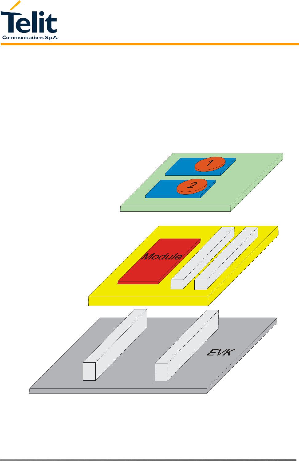
8.2.2EVB for Agilent and Transchip camera support
In order to interface the Telit GM862 with a CMOS camera, Telit has developed an evaluation
board. The EVK allow connecting all Telit modules through 2 connectors of 40 pins each.
The I2CBUS DUAL CAMERA board is plugged in the 2 connectors of 30 pins each on the module
board.
MODULE
BOARD
MAIN
BOARD
CAMERA
BOARD
Telit GM862-QUAD/-QUAD-PY
Hardware User Guide
1vv0300692, Rev. ISSUE#0, - 04/10/2005
Reproduction forbidden without DAI Telecom written authorization – All Right reserved – Right of modification reserved page 48 of 69
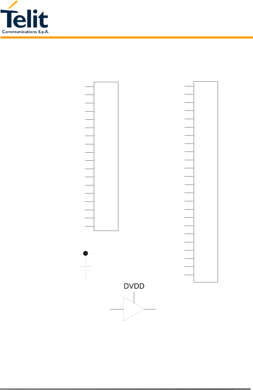
8.2.3Block Diagram for supported cameras
The numbers on the left side of the Camera’s connectors refers to Module Connector’s pin number.
DVDD is an external power supply of 2.8V, controlled or gated by pin CAM_PWR_ON.
1
2
3
4
5
6
7
8
9
10
11
12
13
14
15
16
17
18
GND
DVDD
IICSDA_CAM
IICSCL_CAM
CAM_PWR_ON
CAM_DRDY
PD[7]
CAM_SYNC
CAM_CLK
GND
PD[6]
PD[5]
PD[4]
PD[3]
PD[2]
PD[1]
PD[0]
1
2
3
4
5
6
7
8
9
10
11
12
13
14
15
16
17
18
19
20
21
22
23
24
GND
AVDD
CAM_CLK
GND
DVDD
IICSDA_CAM
GND
GND
PD[1]
PD[0]
PD[6]
CAM_CLK
DVDD AVDD
GND
CAMERA AGILENT CAMERA TRANSCHIP
MON1_CAM
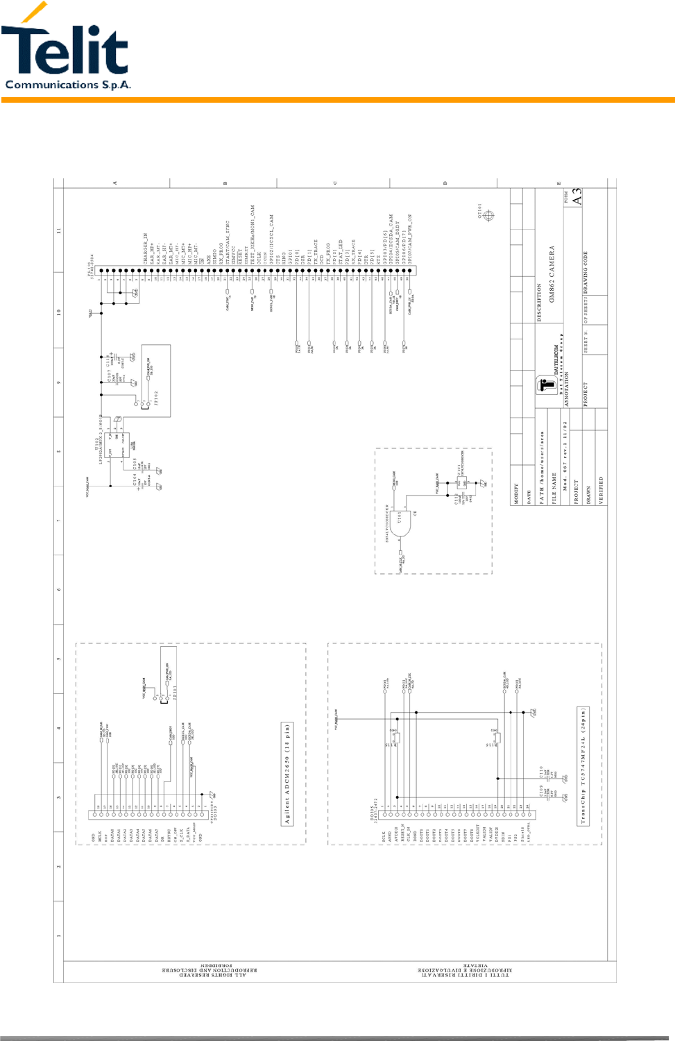
Telit GM862-QUAD/-QUAD-PY
Hardware User Guide
1vv0300692, Rev. ISSUE#0, - 04/10/2005
Reproduction forbidden without DAI Telecom written authorization – All Right reserved – Right of modification reserved page 49 of 69
8.2.4 Schematic Diagrams for supported cameras
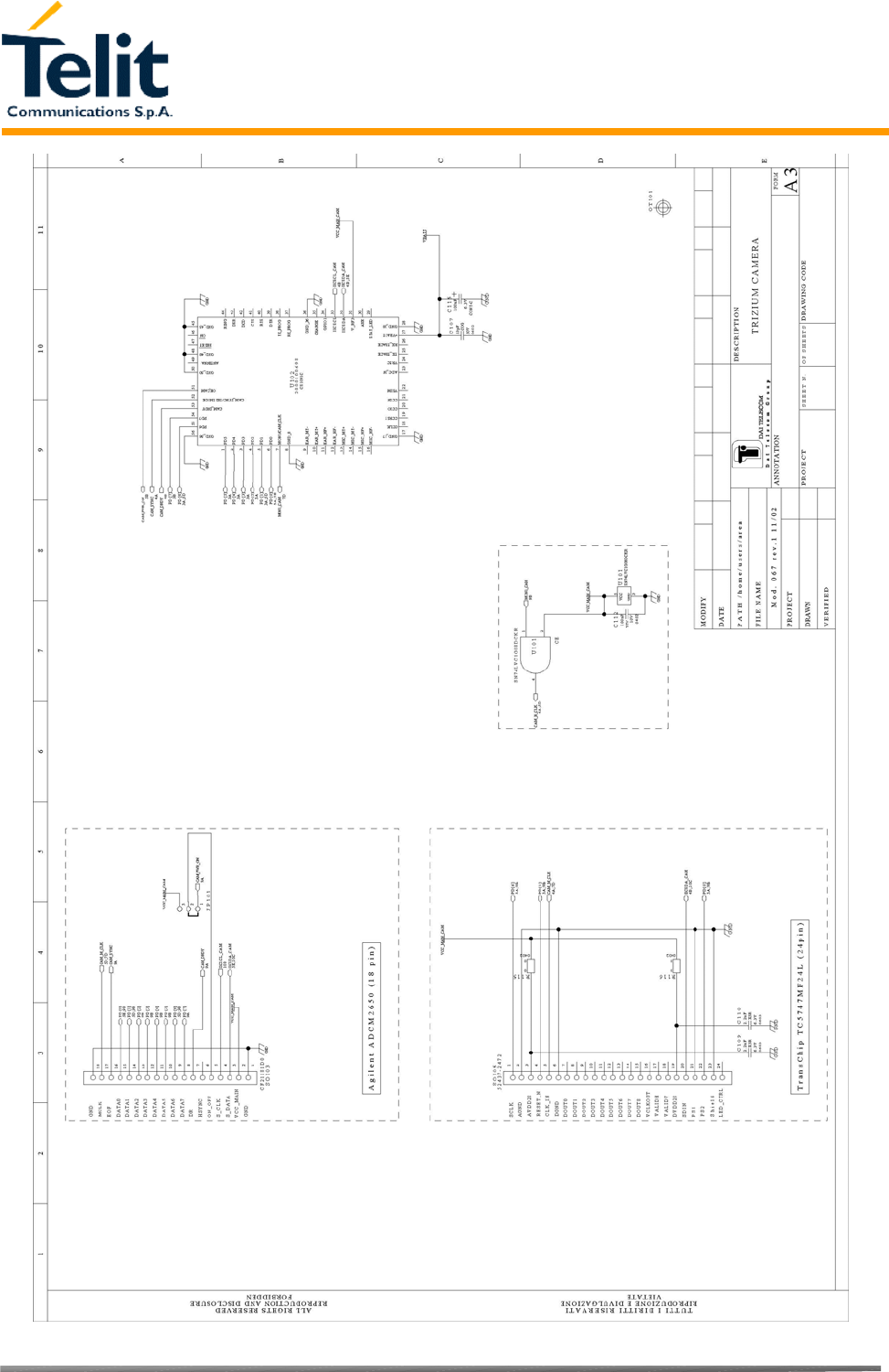
Telit GM862-QUAD/-QUAD-PY
Hardware User Guide
1vv0300692, Rev. ISSUE#0, - 04/10/2005
Reproduction forbidden without DAI Telecom written authorization – All Right reserved – Right of modification reserved page 50 of 69

Telit GM862-QUAD/-QUAD-PY
Hardware User Guide
1vv0300692, Rev. ISSUE#0, - 04/10/2005
Reproduction forbidden without DAI Telecom written authorization – All Right reserved – Right of modification reserved page 51 of 69
8.2.5Example usage script for camera
Camera setting: (shown here are the defaults ones)
>AT#CAMSEL=0 (camera selection: 0-auto, 1-agilent, 2-transchip)
OK
>AT#CMODE=0 (camera mode: 0-day, 1-night)
OK
>AT#CAMQUA=0 (camera quality: 0-low, 1-medieum, 2-high)
OK
>AT#CAMRES=0 (camera resolution: 0-VGA, 1-QVGA, 2-QQVGA)
OK
>AT#CAMCOL=0* (camera color: 0-color, 1-grayscale)
OK
>AT#CAMZOOM=0 (camera zoom: 0-x1, 1-x2, 2-x4)
OK
>AT#CAMTXT=0* (camera timestamp: 0-no, 1-time only, 2-data only, 3-time&data)
OK
Taking an reading a photo:
>AT#CAMEN=1 (camera ON)
OK
>AT#TPHOTO (take photo)
OK
>AT+OBJL? (see photo dimension)
#OBJL: Snapshot,38900 (where 38900 is the file dimension in bytes of the photo taken)
OK
>AT#RPHOTO (download the photo)
…data….. (where …data… Correspond to the photo data in binary)
OK
>AT#TPHOTO
OK
>AT#RPHOTO Repeating photo capture and download n times
…data…..
OK
>AT#CAMEN=O (camera OFF)
*only Transchip camera
Telit GM862-QUAD/-QUAD-PY
Hardware User Guide
1vv0300692, Rev. ISSUE#0, - 04/10/2005
Reproduction forbidden without DAI Telecom written authorization – All Right reserved – Right of modification reserved page 52 of 69
9 Document Change Log
Revision Date Changes

Telit GM862-QUAD/-QUAD-PY
Hardware User Guide
1vv0300692, Rev. ISSUE#0, - 04/10/2005
Reproduction forbidden without DAI Telecom written authorization – All Right reserved – Right of modification reserved page 53 of 69
10 Annex A - EVK schematics
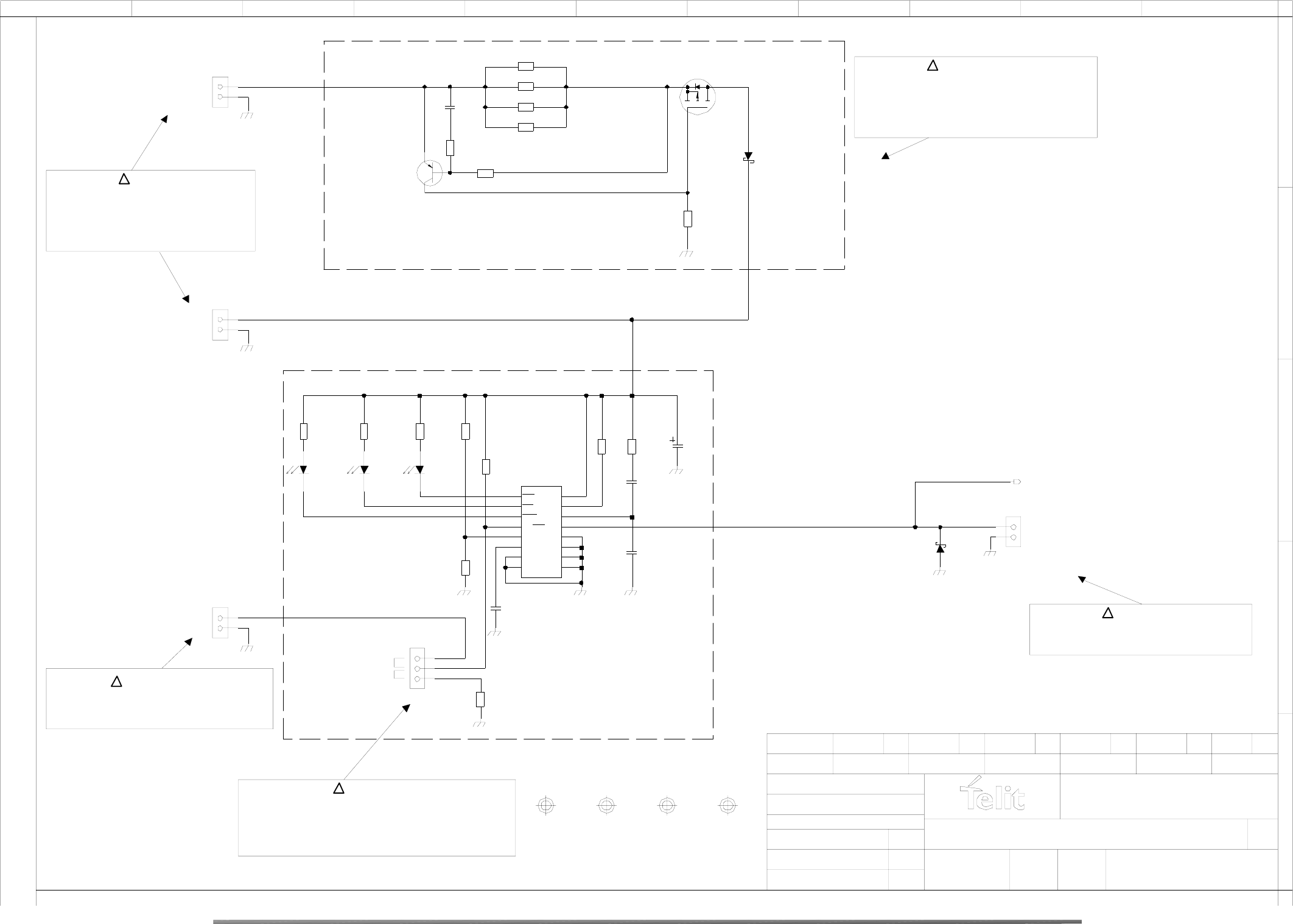
Reproduction forbidden without DAI Telecom written authorization – All Right reserved – Right of modification reserved page 54 of 69
FORBIDDENVIETATE
ALL RIGHTS RESERVED
RIPRODUZIONE E DIVULGAZIONE REPRODUCTION AND DISCLOSURE
TUTTI I DIRITTI RISERVATI
PROJECT A3
DESCRIPTION
DRAWING CODE
FORM
MODIFY
OF SHEETS
DATE
SHEET N.
VERIFIED
PROJECT
DRAWN
PATH /home/users/area
Mod. 067 rev.0 03/01 ANNOTATION
FILE NAME
B
C
D
E
A
Mobile Terminals S.p.A.
42 981 0713 1165
GND
50V
0603
68nF
X7R
C104
GND
CR32
4.7
10%
R105
CR32
4.7
10%
R102
CR32
4.7
10%
R103
CR32
4.7
10%
R104
STPS340U
SMB
U34
D107
35V
CONT-A
1uF
C105
GND
.
2SJ387S
DPAK-2S
Q102
2
D
3S1
G
GND
FCMM0502
SO104
2
1
GND
FCMM0502
SO101
2
1
1215061-03F
PL101
2
1
3
GND
STPS140Z
SOD123
D106
+VBATT
002:11D
GND
LY-T670HK
PLCC2
YELLOW
DL101
OT101 OT102 OT103 OT104
FCMM0502
SO103
2
1
GND
0603
10K
5%
R101
3Fs
BC857B
SOT-23
Q101 2
3
1
0603
5.6K
5%
R106
0603
680
5%
R107
50V
0603
4.7nF
X7R
C101
LTC1730EGN-4
U101
14 NC_14
5FAULT
1
GND_1
11 NTC/SHDN
10 TIMER 8
GND_8
3
VCC
4ACPR
16
GND_16
9
GND_9
2
SENSE
13
GATE
12 SEL
6CHRG
7NC_7
15
BAT
LY-T670HK
PLCC2
YELLOW
DL102
LS-T670HK
PLCC2
RED
DL103
GND
LR32
0.1
5%
R108
50V
0603
47nF
X7R
C102
50V
0603
220pF
X7R
C103
0603
10K
5%
R109
GND
0603
10K
5%
R111
GND
0603
4.3K
5%
R110
FCMM0502
SO102
2
1
0603
1K
5%
R112
0603
1K
5%
R113
0603
1K
5%
R114
GND
0603
0
5%
R115
0603
0
5%
R116
noMount=YES
041201
041201
EVK for GM862/S1
0208
301101
Locatelli M. 1 30208SE10944b
cs944b.cir
10
Deperini F. BATTERY CHARGE CONTROL
ON CHARGE
NTC enabled
NTC disabled
Temperature sensing control
WARNING!!!!
When the temperature sensing is disabled
the charger must be powered ONLY if the
battery temperature is within the charging
!
BATTERY CHARGER INPUT +
-
6 Vcc
3,7V(Li-Ion) Nominal
BATTERY LI-ION
+
-
current limit: 500 mA
max voltage 4,2V (Li-Ion)
Li - Ion battery charger
max current ~ 1 A
Current Limiting Circuit
polarity is respected!
! WARNING!!!!
When using battery care must be
taken to ensure that the right
WARNING!!!!
Max current limit must be properly
set for the size of battery in use
Keep max current around 1/2 of
!
battery pack capacity
E.g. 1000mAh -> 500 mA max
CURRENT UNLIMITED
BATTERY CHARGER INPUT -
+
4.5 - 10 Vcc
CURRENT LIMITED
CHARGER PRESENCE
FAULT
Temperature sensor
10k NTC
Otherwise the battery may explode!
range 0 - 50 C.
power input is respected!
! WARNING!!!!
Care must be taken to ensure
that the right polarity in the
WARNING!!!!
For a proper battery temperature
sensing the Termistor should be
placed on the battery pack.
!
DO NOT Supply power when the
Battery is not connected
Otherwise GM862 may be damaged!
Curr. limit is given by R102 to R105
suggested capacity: 1000mAh
Serdi M.
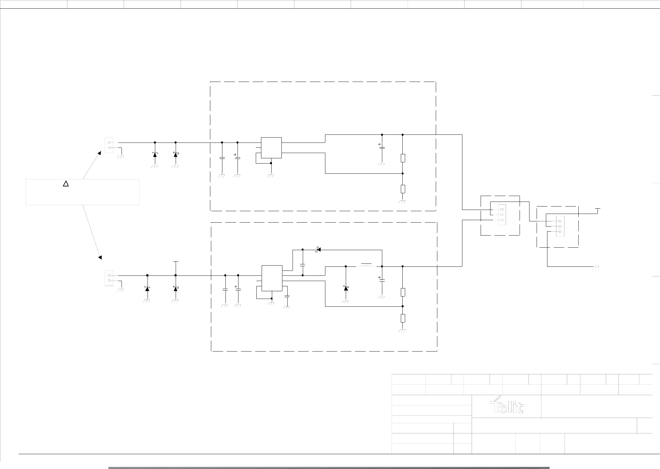
Reproduction forbidden without DAI Telecom written authorization – All Right reserved – Right of modification reserved page 55 of 69
FORBIDDENVIETATE
ALL RIGHTS RESERVED
RIPRODUZIONE E DIVULGAZIONE REPRODUCTION AND DISCLOSURE
TUTTI I DIRITTI RISERVATI
PROJECT A3
DESCRIPTION
DRAWING CODE
FORM
MODIFY
OF SHEETS
DATE
SHEET N.
VERIFIED
PROJECT
DRAWN
PATH /home/users/area
Mod. 067 rev.0 03/01 ANNOTATION
FILE NAME
B
C
D
E
A
Mobile Terminals S.p.A.
42 981 0713 1165
GND
STPS140Z
SOD123
D206
noMount=YES
STPS140Z
SOD123
D205
noMount=YES
+VBATT
001:9C
GND
+12V
0603
4.7K
5%
R204
LT1374CR
U202
5VIN
4GND_1 1
VC
3
VSW
2SHDN*
GND_2
8
7
SENSE
6
BOOST
35V
CONT-E
10uF
C206
0603
2.7K
5%
R203
GND
0603
47
5%
R202
FCMM0502
SO201
2
1
25V
0603
39nF
X7R
C203
GND
GND
GND
GND
50V
0603
1.5nF
X7R
C208
DO3316
10uH
L201
GND
10V
CONT-D
100uF
C204
GND
10V
CONT-D
100uF
C201
0603
470nF
6.3V
X5R
C209
GND
GND
GND
25V
0603
39nF
X7R
C207
.
6KA24
6KA24
DZ201
GND
GND
.
6KA24
6KA24
DZ202
35V
CONT-E
10uF
C202
STPS140Z
SOD123
D201
GND
+3.7V
FCMM0502
SO202
2
1
GND
GND GND
.
BAT62-02W
SCD-80
D202
LT1528CQ
U201
5V_IN
3GND 2
SENSE
1
V_OUT
4SHDN*
GND_1
6
0603
330
5%
R201
1215061-03F
PL201
2
1
3
1215061-03F
PL202
2
1
3
100208
041201
EVK for GM862/S1
301101Deperini F.
041201
30208SE10944b
Serdi M.
cs944b.cir
2
+5V/+12V INPUT POWER REGULATORS
Locatelli M.
-
+5V INPUT
4,5V-8 Vcc
+
8-15,8V Vcc
+
-
+12V INPUT
power input is respected!
! WARNING!!!!
Care must be taken to ensure
that the right polarity in the +5V/+12V select
Battery/Regulator select
+5V input linear regulator
+12V input switching regulator
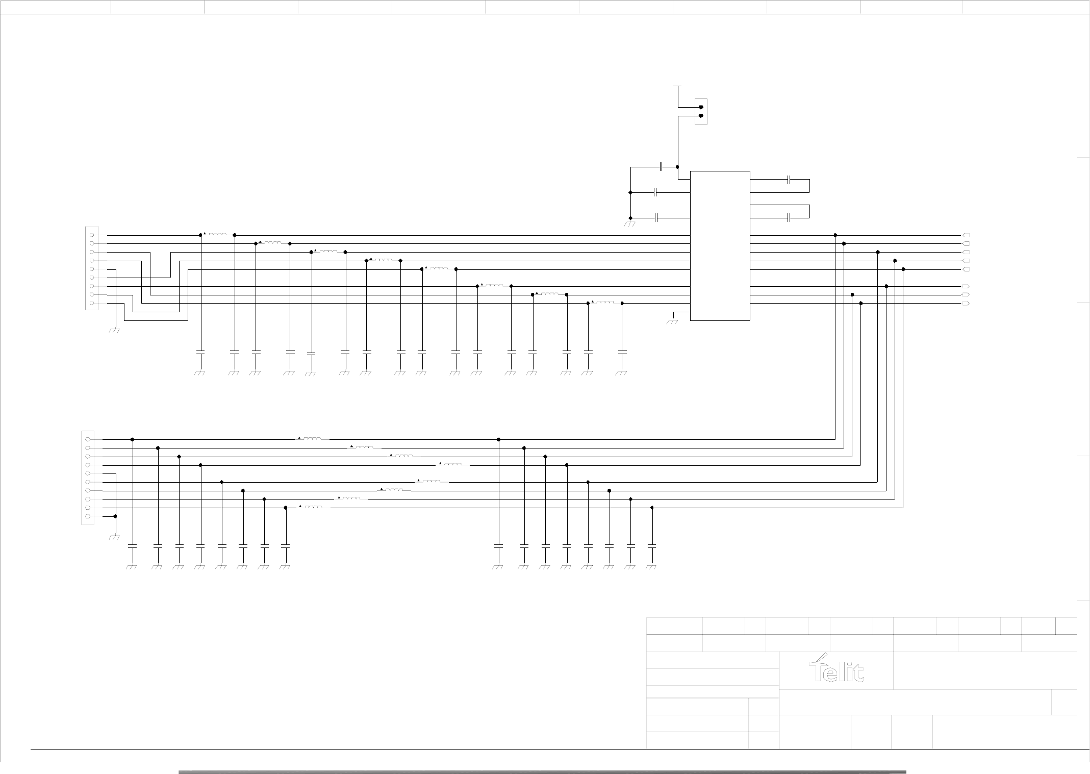
Reproduction forbidden without DAI Telecom written authorization – All Right reserved – Right of modification reserved page 56 of 69
LQG18HN39NJ00
LQG18
39nH
L305
GND
10V
0603
220nF
X7R
C302
TX_PROG
004:6D
LQG18HN39NJ00
LQG18
39nH
L302
LQG18HN39NJ00
LQG18
39nH
L308
LQG18HN39NJ00
LQG18
39nH
L304
+3.7V
RX_PROG
004:5D
50V
0603
1nF
X7R
C307
50V
0603
1nF
X7R
C309
50V
0603
1nF
X7R
C308
LQG18HN39NJ00
LQG18
39nH
L303
LQG18HN39NJ00
LQG18
39nH
L307 LQG18HN39NJ00
LQG18
39nH
L306
10V
0603
220nF
X7R
C304
LQG18HN39NJ00
LQG18
39nH
L301
DTR
004:6D
16V
0603
100nF
X7R
C305
FORBIDDENVIETATE
ALL RIGHTS RESERVED
RIPRODUZIONE E DIVULGAZIONE REPRODUCTION AND DISCLOSURE
TUTTI I DIRITTI RISERVATI
PROJECT A3
DESCRIPTION
DRAWING CODE
FORM
MODIFY
OF SHEETS
DATE
SHEET N.
VERIFIED
PROJECT
DRAWN
PATH /home/users/area
Mod. 067 rev.0 03/01 ANNOTATION
FILE NAME
B
C
D
E
A
Mobile Terminals S.p.A.
42 981 0713 1165
50V
0603
1nF
X7R
C306
10V
0603
220nF
X7R
C303
GND
RTS
004:6D
10V
0603
220nF
X7R
C301
ICL3207CA
SSOP-24
U301
6
T2_IN
15 V-
19
T4_IN
21
T5_IN
20 T5_OUT
24 T4_OUT
1TR3_OUT
2T1_OUT
14
C2-
13
C2+
16 R3_IN
5
R1_OUT
22
R2_OUT
17
R3_OUT
3T2_OUT
10
C1+
12
C1-
7
T1_IN
18
T3_IN
11 V+
9VCC
23 R2_IN
4R1_IN
8GND_8
GND
1615061-10F
PL301
3
2
1
4
5
6
7
8
9
10
RING
004:5D
DCD
004:6D
CTS
004:5D
787200-1
SO301
3
2
1
4
5
6
7
8
9
GND
50V
0603
39pF
COG
C336
50V
0603
39pF
COG
C333
GND
50V
0603
39pF
COG
C335
50V
0603
39pF
COG
C337
LQG18HN39NJ00
LQG18
39nH
L312
LQG18HN39NJ00
LQG18
39nH
L313
LQG18HN39NJ00
LQG18
39nH
L314
50V
0603
39pF
COG
C331
LQG18HN39NJ00
LQG18
39nH
L315
50V
0603
39pF
COG
C330
LQG18HN39NJ00
LQG18
39nH
L316
50V
0603
39pF
COG
C321
GND
50V
0603
39pF
COG
C318
GND
DSR
004:5D
GND
50V
0603
1nF
X7R
C326
50V
0603
1nF
X7R
C311
GND
GND
50V
0603
1nF
X7R
C310
GND
50V
0603
1nF
X7R
C329
50V
0603
39pF
COG
C317
50V
0603
39pF
COG
C332
50V
0603
1nF
X7R
C328
GND
50V
0603
39pF
COG
C320
GND
LQG18HN39NJ00
LQG18
39nH
L309
50V
0603
39pF
COG
C319
50V
0603
1nF
X7R
C322
50V
0603
1nF
X7R
C324
GND
50V
0603
1nF
X7R
C312
50V
0603
1nF
X7R
C327
GNDGND
50V
0603
1nF
X7R
C313
50V
0603
1nF
X7R
C323
GND
50V
0603
39pF
COG
C314
GND GNDGND
GND
GND GND
GND
50V
0603
1nF
X7R
C325
GND
GNDGND
GND
LQG18HN39NJ00
LQG18
39nH
L310
GND
50V
0603
39pF
COG
C334
LQG18HN39NJ00
LQG18
39nH
L311
GNDGND
GND
GND GND GND
50V
0603
39pF
COG
C316
50V
0603
39pF
COG
C315
GND
1215061-02F
PL302
2
1
30208SE10944b31 0
301101
Serdi M.
RS232 LEVEL TRANSLATOR AND UART INPUT/OUTPUT
0208
cs944b.cir
Locatelli M.
Deperini F.
041201
041201
EVK for GM862/S1
+3.7V UART
DCD
RXD
TXD
DTR
DSR
RTS
CTS
RI
GND
GND
TO RS232
GND
DSR
DCD
TXD
RXD
DTR
RTS
RI
CTS
RS232 LEVEL TRANSLATOR POWER SELECTION
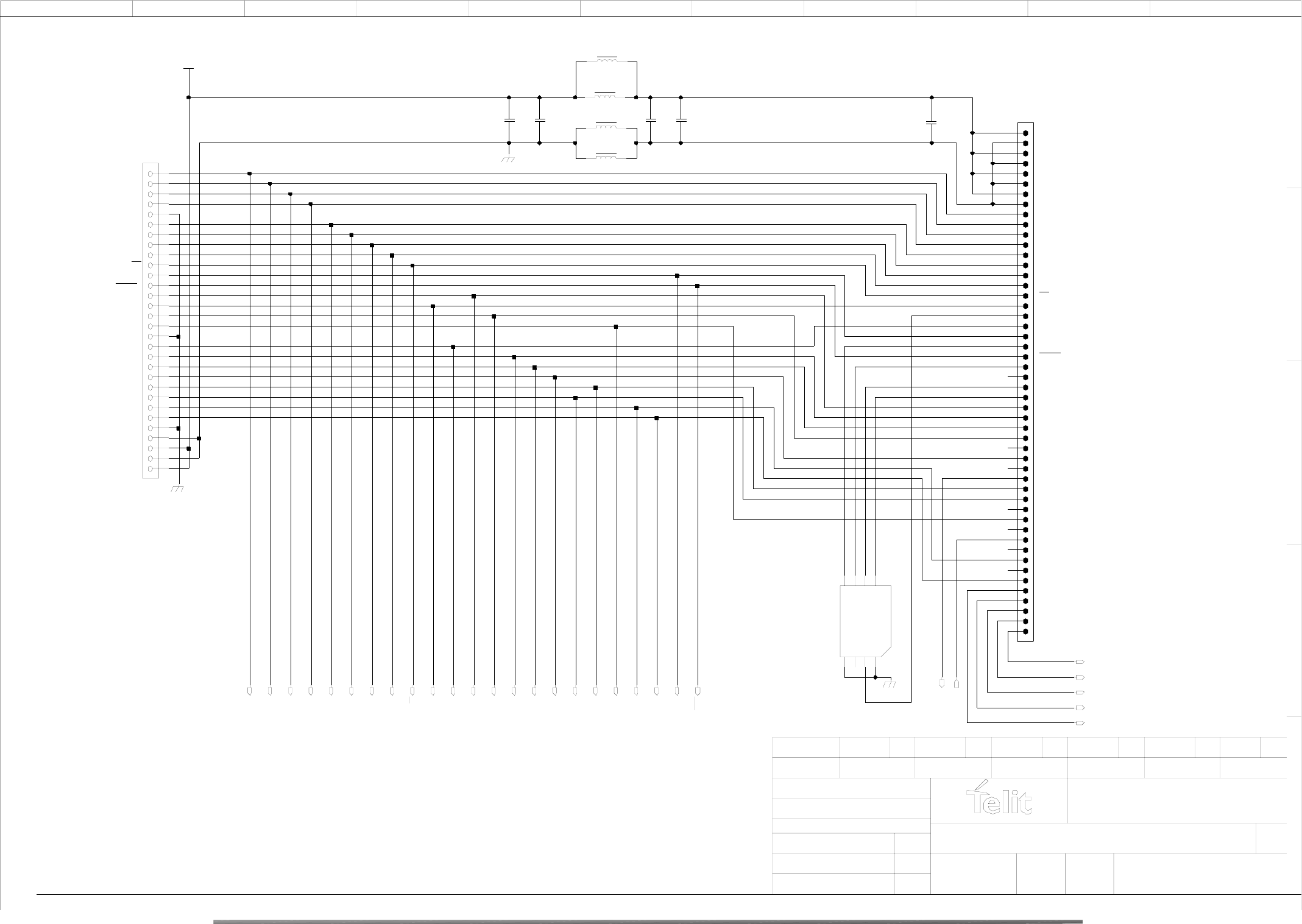
Reproduction forbidden without DAI Telecom written authorization – All Right reserved – Right of modification reserved page 57 of 69
4773541130470
SO402
3
2
1
4
5
6
7
8
9
10
11
12
13
14
15
16
17
18
19
20
21
22
23
24
25
26
27
28
29
30
50V
0603
100pF
COG
C402
RESET
005:9B
16V
0603
100nF
X7R
C403
START
005:3D
TX_PROG
003:10B
GND
MIC_HF+
007:11C
DTR
003:10C
STAT_LED
005:9C
GND
ON
005:10A
GPIO1
005:7C;006:10D
AXE
005:7E
DSR
003:10B
EAR_HF-
008:10D;009:11C
MIC_MT+
006:10B
RING
003:10B
EAR_MT+
006:10E;008:10B
RTS
003:10C
50V
0603
33pF
COG
C401
RX_PROG
003:10C
CTS
003:10B
EAR_HF+
008:10D;009:11B
50V
0603
100pF
COG
C404
16V
0603
100nF
X7R
C405
GND
53748-0504
PL401
3
2
1
4
5
6
7
8
9
10
11
12
13
14
15
16
17
18
19
20
21
22
23
24
25
26
27
28
29
30
31
32
33
34
35
36
37
38
39
40
41
42
43
44
45
46
47
48
49
50
BLM21
220
L403
MIC_MT-
006:10C
EAR_MT-
006:10D;008:10B
+3.7V
BLM21
220
L404
4312-020
0.35
noMount=YES
L402
GPIO2
005:6A
MIC_HF-
007:11D
DCD
003:10B
4312-020
0.35
noMount=YES
L401
FORBIDDENVIETATE
ALL RIGHTS RESERVED
RIPRODUZIONE E DIVULGAZIONE REPRODUCTION AND DISCLOSURE
TUTTI I DIRITTI RISERVATI
PROJECT A3
DESCRIPTION
DRAWING CODE
FORM
MODIFY
OF SHEETS
DATE
SHEET N.
VERIFIED
PROJECT
DRAWN
PATH /home/users/area
Mod. 067 rev.0 03/01 ANNOTATION
FILE NAME
B
C
D
E
A
Mobile Terminals S.p.A.
42 981 0713 1165
SIM_CARD
52827-0611
SO401
1
C1
6C6
5C5
4
C4
3
C3
2
C2
7C7
8C8
RX_TRACE
010:9C
TX_TRACE
010:9B
GPIO3
005:11D
GPIO4
005:11D
GPIO5
005:11D
GPIO6
005:11D
GPIO7
005:11D
Serdi M.
GM862 & S1 CONNECTORS
041201 4
Locatelli M.
041201
0208
Deperini F.
10 30208SE10944b
EVK for GM862/S1
cs944b.cir
301101
AXE
JP105
DTR
SIMRST
GPI01
EAR_MT-
JP103
TX_PROG
TX_TRACE
SIMRST
MIC_HF-
SIMIO
EAR_HF+
EAR_HF+
RX_TRACE
SIMVCC
EAR_MT+
GPI02
DCD
MIC_MT-
START
EAR_HF-
EAR_MT-
RX_PROG
JP104
SIMCLK
SIMVCC
MIC_MT-
MIC_HF+
CTS
TEST_32KHz
GND_EXT
MIC_HF-
JP101
AXE
DSR
JP102
ON
MIC_MT+
MIC_MT+
RTS
RING
EAR_HF-
CCIN
MIC_HF+
JP106
SIMIO
STAT_LED
CCIN
EAR_MT+MIC_HF+
EAR_MT+
GPI02
MIC_MT-
GND
AXE
DCD
DSR
EAR_MT-
CTS
+3.7V
DTR
PWR_GND
RTS
GND
RX_PROG
EAR_HF-
ON
START
STAT_LED
RESET
MIC_HF-
TX_PROG
RING
MIC_MT+
EAR_HF+
GPI01
S1 CONNECTOR
GM862 CONNECTOR
SIMCLK
RESET
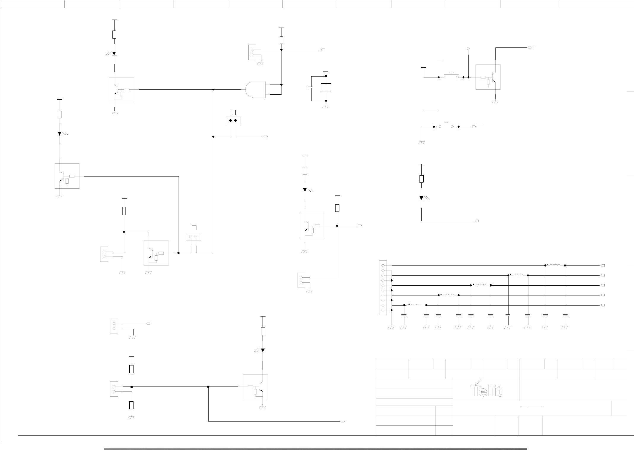
Reproduction forbidden without DAI Telecom written authorization – All Right reserved – Right of modification reserved page 58 of 69
GND
0603
1K
5%
R508
+3.7V
+3.7V
0603
10K
5%
R509
1215061-02F
PL506
2
1
GND
+3.7V
0603
22K
5%
R510
GPIO1
004:5D;006:10D
MUTE
008:10B;008:10D;009:11C
1215061-02F
PL504
2
1
AXE
004:4D
1215061-02F
PL505
2
1
0603
560
5%
R503
GPIO2
004:5D
0603
560
5%
R504
LY-T670HK
PLCC2
YELLOW
DL504
GND
GND
0603
560
5%
R502
GND
47K
47K
WEs
BCR148W
SOT-323
Q506
2
3
1
LY-T670HK
PLCC2
YELLOW
DL503
FORBIDDENVIETATE
ALL RIGHTS RESERVED
RIPRODUZIONE E DIVULGAZIONE REPRODUCTION AND DISCLOSURE
TUTTI I DIRITTI RISERVATI
PROJECT A3
DESCRIPTION
DRAWING CODE
FORM
MODIFY
OF SHEETS
DATE
SHEET N.
VERIFIED
PROJECT
DRAWN
PATH /home/users/area
Mod. 067 rev.0 03/01 ANNOTATION
FILE NAME
B
C
D
E
A
Mobile Terminals S.p.A.
42 981 0713 1165
SKHHAL
SW501
31
24
RESET
004:7D
SKHHAL
SW502
31
24
ON
004:4D
GND
+3.7V
LY-T670HK
PLCC2
YELLOW
DL502
0603
100
5%
R501
GND
1215061-02F
PL502
2
1
+3.7V
LY-T670HK
PLCC2
YELLOW
DL501
GND
GND
0603
10K
5%
R506
noMount=YES
+3.7V
STAT_LED
004:6D
+12V
+3.7V
LY-T670HK
PLCC2
YELLOW
DL505
+3.7V
0603
560
5%
R505
START
004:6D
GND
1215061-02F
PL501
2
1
+3.7V
1215061-02F
PL503
2
1
GND
0603
0
5%
R507
TP501
47K
47K
WEs
BCR148W
SOT-323
Q502 2
3
1
47K
47K
WEs
BCR148W
SOT-323
Q504
2
3
1
47K
47K
WEs
BCR148W
SOT-323
Q503 2
3
1
47K
47K
WEs
BCR148W
SOT-323
Q507 2
3
1
E2
TC7S08FU
U501
2
4
1
TC7S08FU
U501
5
VCC_1
3
GND_1
+3.7V
GND
16V
0603
100nF
Y5V
C501
47K
47K
WEs
BCR148W
SOT-323
Q508 2
3
1
GND
1215061-02F
PL507
2
1
LQG18HN39NJ00
LQG18
39nH
L501
50V
0603
39pF
COG
C510
GNDGND
50V
0603
1nF
X7R
C511
50V
0603
39pF
COG
C508
50V
0603
1nF
X7R
C509
LQG18HN39NJ00
LQG18
39nH
L505
GNDGND
LQG18HN39NJ00
LQG18
39nH
L504
GND
50V
0603
39pF
COG
C506
50V
0603
1nF
X7R
C507
GND
LQG18HN39NJ00
LQG18
39nH
L503
GND
50V
0603
39pF
COG
C504
50V
0603
1nF
X7R
C505
GND
LQG18HN39NJ00
LQG18
39nH
L502
GND
50V
0603
39pF
COG
C502
50V
0603
1nF
X7R
C503
GND
GPIO7
004:10E
GPIO6
004:10E
GPIO5
004:10D
GPIO3
004:10D
GPIO4
004:10D
1615061-10F
PL508
3
2
1
4
5
6
7
8
9
10
GND
0208
041201
301101Deperini F.
5
cs944b.cir
10
Locatelli M. 30208SE10944b
Serdi M. 041201
EVK for GM862/S1
AUX PINS, STATE LEDS AND ON/RESET BUTTONS
YELLOW - STAT LED
GREEN - GPIO1 LED
GREEN - GPIO2 LED
GREEN - AXE LED
EXTERNAL ACCESSORIES
RESET BUTTON
ON BUTTON
POWER ON OUTPUT
GREEN - STEREO MUTE LED
CAR STEREO MUTE OUTPUT
EXTERNAL ACCESSORIES
SENSE INPUT
EXTERNAL ACCESSORIES
GPIO1 INPUT
GPIO2 OUTPUT
MUTE CONTROL SELECT
GPIO2
MUTE CONTROL
GPIO2
CAR STEREO
GPIO (GPRS) CONNECTOR
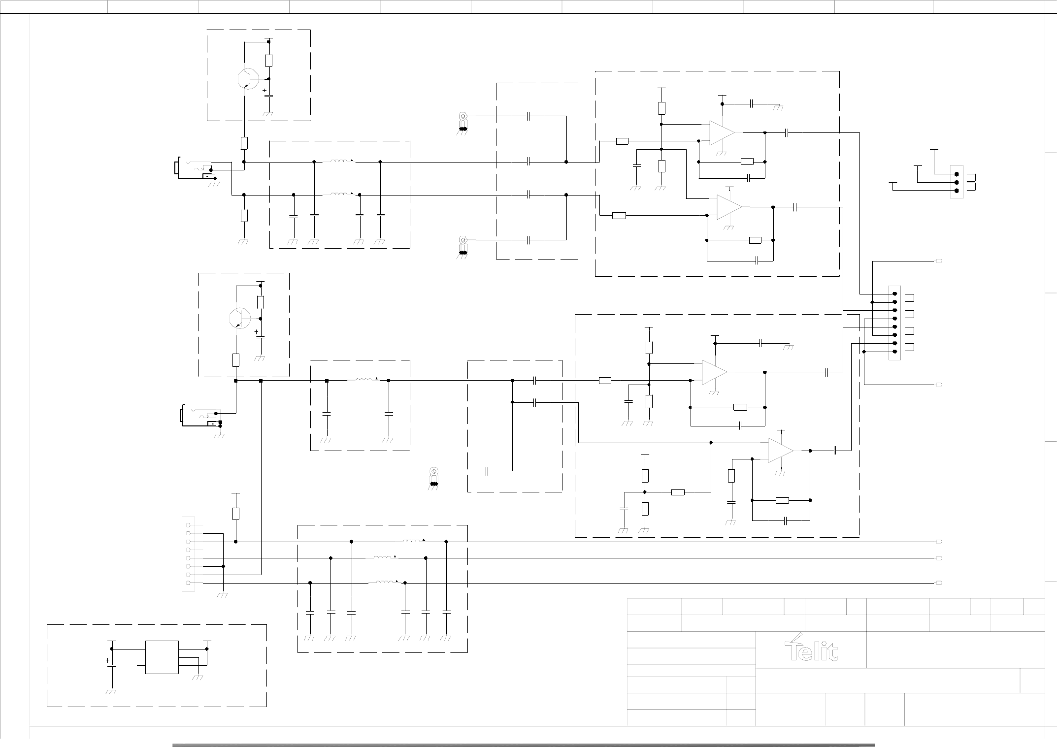
Reproduction forbidden without DAI Telecom written authorization – All Right reserved – Right of modification reserved page 59 of 69
FORBIDDENVIETATE
ALL RIGHTS RESERVED
RIPRODUZIONE E DIVULGAZIONE REPRODUCTION AND DISCLOSURE
TUTTI I DIRITTI RISERVATI
PROJECT A3
DESCRIPTION
DRAWING CODE
FORM
MODIFY
OF SHEETS
DATE
SHEET N.
VERIFIED
PROJECT
DRAWN
PATH /home/users/area
Mod. 067 rev.0 03/01 ANNOTATION
FILE NAME
B
C
D
E
A
Mobile Terminals S.p.A.
42 981 0713 1165
+3V_INT_MIC_BAL
16V
0603
100nF
Y5V
C602
GND
GND
50V
0603
39pF
COG
C613
1615061-08F
PL602
3
2
1
4
5
6
7
8
GND
+3V_INT_MIC_BAL
50V
0603
1nF
X7R
C614
LQG18HN39NJ00
LQG18
39nH
L602
LQG18HN39NJ00
LQG18
39nH
L603
GND
1Fs
BC847BW
SOT-323
Q602 2
3
1
MIC_MT-
004:4D
EAR_MT+
004:3D;008:10B
+3V_MIC
16V
0603
100nF
Y5V
C617
0603
82K
5%
R610
0603
10K
5%
R611
GND
GND
50V
0603
1nF
X7R
C616
0603
10K
5%
R605
0603
10K
5%
R607
GND
GND
LQG18HN39NJ00
LQG18
39nH
L605
0603
2.2K
5%
R608
16V
0603
100nF
Y5V
C627
0603
150K
5%
R606
GND
50V
0603
1nF
X7R
C615
GND
95001-6881
SO603
3
2
1
4
5
6
7
8
+3V_MIC
LQG18HN39NJ00
LQG18
39nH
L606
TS3V912ID
U602
4
V-
8
V+ 1
OUT
2-
3+
GND
16V
0603
100nF
Y5V
C606
0603
47K
5%
R612
noMount=YES
35V
CONT-E
10uF
C605
GND
GND
GND
GND
50V
0603
1nF
X7R
C619
50V
0603
39pF
COG
C624
4V
CONT-R
4.7uF
C601
50V
0603
100pF
COG
C637
LQG18HN39NJ00
LQG18
39nH
L604
16V
0603
100nF
Y5V
C611
GND
LGK2009-0201
LGK2009-02
SO602
3
4
2
15
50V
0603
39pF
COG
C612
+3.7V
16V
0603
100nF
Y5V
C604
0603
47K
5%
R615
50V
0603
39pF
COG
C607
GND
0603
10K
5%
R609
16V
0603
100nF
Y5V
C628
4V
CONT-R
4.7uF
C610
GPIO1
004:5D;005:7C
GND
GND
GND
16V
0603
100nF
Y5V
C609
50V
0603
1nF
X7R
C620
GND
TS3V912ID
U602
4
V-
8
V+ 7
OUT
6-
5+
0603
82K
5%
R618
0603
1K
5%
R603
GND
LGK2009-0201
LGK2009-02
SO601
3
4
2
15
0603
470K
5%
R619
16V
0603
100nF
Y5V
C608
0603
47K
5%
R613
0603
150K
5%
R604
GND
50V
0603
1nF
X7R
C623
GND
0603
47K
5%
R616
GND
LQG18HN39NJ00
LQG18
39nH
L601
0603
47K
5%
R614
J01001A1944
SO605
1
IO
2
3
4
5
GND
MIC_MT+
004:4D
0603
1K
5%
R602
16V
0603
100nF
Y5V
C631
GND
16V
0603
100nF
Y5V
C632
50V
0603
39pF
COG
C622
GND
1215061-03F
PL603
2
1
3
TS3V912ID
U603
4
V-
8
V+ 7
OUT
6-
5+
TS3V912ID
U603
4
V-
8
V+ 1
OUT
2-
3+
1Fs
BC847BW
SOT-323
Q601 2
3
1
50V
0603
220pF
X7R
C635
0603
10K
5%
R617
0603
220pF
C634
50V
X7R
16V
0603
100nF
Y5V
C633
J01001A1944
SO606
1
IO
2
3
4
5
L02A
LP2980AIM5X-3_0
MA05B
U601
1
V_IN
3
ON-OFF
4NC
5V_OUT
2
GND
0603
10K
5%
R601
+3V_MIC
0603
47K
5%
R621
GND
16V
0603
100nF
Y5V
C625
J01001A1944
SO604
1
IO
2
3
4
5
GND
GND
GND
0603
47K
5%
R620
16V
0603
100nF
Y5V
C626
16V
0603
100nF
Y5V
C630
50V
0603
100pF
COG
C636
GND
+3V_INT_MIC_BAL
+3V_INT_MIC_BAL
16V
0603
100nF
Y5V
C618
+3V_INT_MIC_SINGLE
+3V_INT_MIC_SINGLE
+3V_INT_MIC_SINGLE
EAR_MT-
004:3D;008:10B
50V
0603
39pF
COG
C621
+3V_INT_MIC_SINGLE
+3V_INT_MIC_SINGLE
GND
+3V_INT_MIC_SINGLE
GND
16V
0603
100nF
Y5V
C603
+3V_INT_MIC_BAL
GND
EVK for GM862/S1
0208 6 10 30208SE10944b
cs944b.cir
INTERNAL MICROPHONE SECTION
BALANCED
SINGLE ENDED
BALANCED
INTERNAL MIC
INTERNAL MIC
SINGLE ENDED
HANDSET V125
BOOT RX
GND
HOOK
BOOT TX
EAR-
MICR+
MICR-
EAR+
SINGLE ENDED
BALANCED
BALANCED MICROPHONE POLARIZATION
SINGLE ENDED MICROPHONE POLARIZATION
MICROPHONE POLARIZATION REGULATOR
SIGNAL FILTERING
SIGNAL FILTERING
BALANCED MICROPHONE BUFFER +24 dB
DECOUPLING CAPACITORS
DECOUPLING CAPACITORS
SINGLE ENDED MICROPHONE BUFFER +24 dB
SIGNAL FILTERING
INT_MIC+
INT_MIC-
INT_MIC
SINGLE ENDED
INT MIC POWER SELECTION
BALANCED
INT MIC SELECTION
Serdi M. 041201
041201
301101
Locatelli M.
Deperini F.
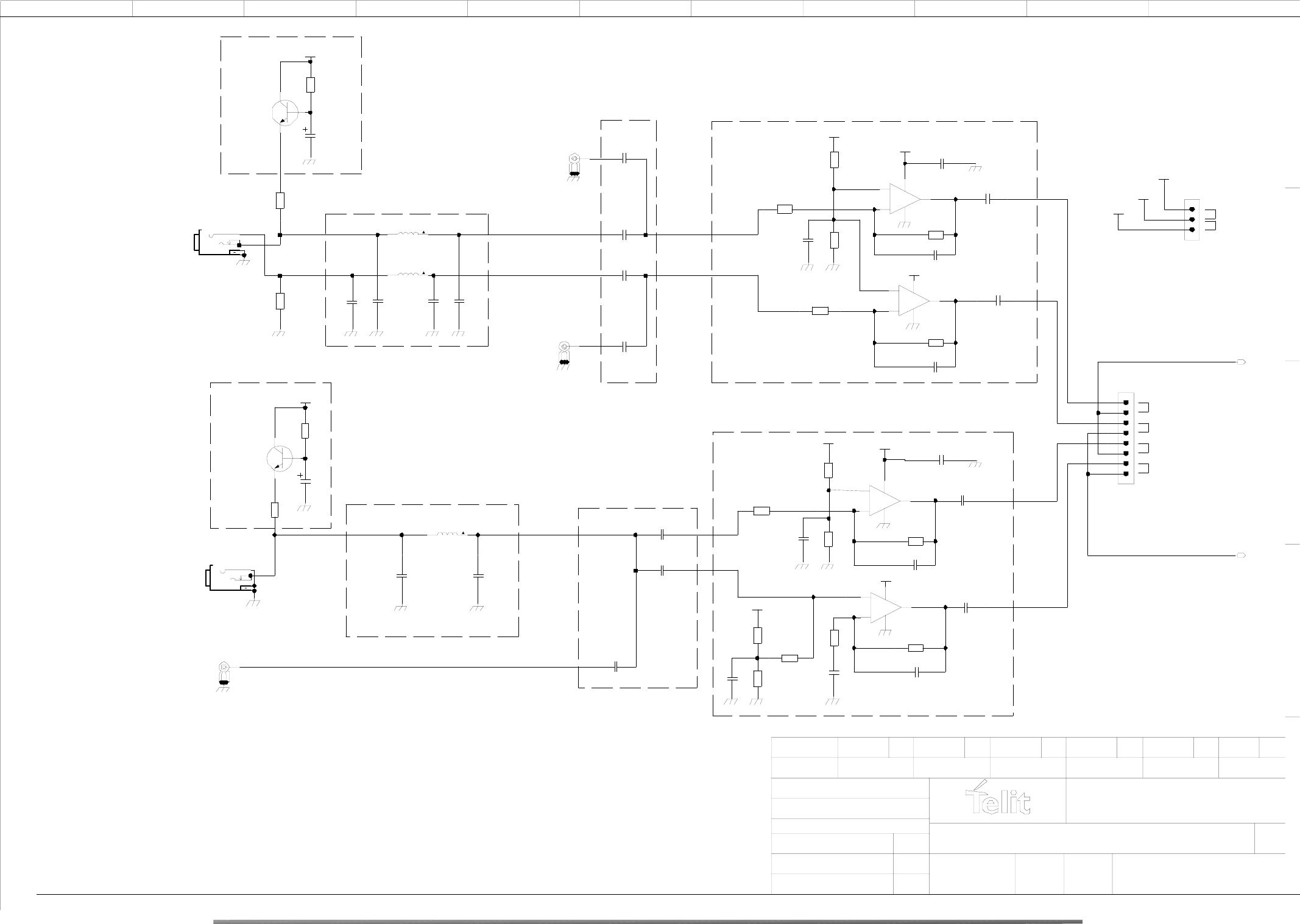
Reproduction forbidden without DAI Telecom written authorization – All Right reserved – Right of modification reserved page 60 of 69
FORBIDDENVIETATE
ALL RIGHTS RESERVED
RIPRODUZIONE E DIVULGAZIONE REPRODUCTION AND DISCLOSURE
TUTTI I DIRITTI RISERVATI
PROJECT A3
DESCRIPTION
DRAWING CODE
FORM
MODIFY
OF SHEETS
DATE
SHEET N.
VERIFIED
PROJECT
DRAWN
PATH /home/users/area
Mod. 067 rev.0 03/01 ANNOTATION
FILE NAME
B
C
D
E
A
Mobile Terminals S.p.A.
42 981 0713 1165
1Fs
BC847BW
SOT-323
Q702 2
3
1
50V
0603
1nF
X7R
C708
LQG18HN39NJ00
LQG18
39nH
L702
GND
J01001A1944
SO704
1
IO
2
3
4
5
J01001A1944
SO703
1
IO
2
3
4
5
50V
0603
39pF
COG
C705
GND
0603
10K
5%
R704
50V
0603
470pF
X7R
C729
GND
0603
47K
5%
R713
50V
0603
1nF
X7R
C706
GND GND
GND
GND
50V
0603
39pF
COG
C704
MIC_HF+
004:4D
50V
0603
1nF
X7R
C727
1215061-03F
PL702
2
1
3
50V
0603
1nF
X7R
C707
16V
0603
100nF
Y5V
C716
LGK2009-0201
LGK2009-02
SO701
3
4
2
15
GND
GND
GND
50V
0603
3.3nF
X7R
C726
1Fs
BC847BW
SOT-323
Q701 2
3
1
0603
47K
5%
R712
GND
LQG18HN39NJ00
LQG18
39nH
L703
16V
0603
100nF
Y5V
C712
16V
0603
100nF
Y5V
C721
16V
0603
100nF
Y5V
C719
16V
0603
100nF
Y5V
C718
GND
GND
0603
15K
5%
R711
+3V_EXT_MIC_SINGLE
GND
GND
1615061-08F
PL701
3
2
1
4
5
6
7
8
0603
33K
5%
R709
+3V_EXT_MIC_BAL
GND
TS3V912ID
U701
4
V-
8
V+ 1
OUT
2-
3+
16V
0603
100nF
Y5V
C722
+3V_EXT_MIC_SINGLE
0603
47K
5%
R717
+3V_EXT_MIC_BAL
J01001A1944
SO705
1
IO
2
3
4
5
+3V_EXT_MIC_SINGLE
0603
10K
5%
R708
TS3V912ID
U701
4
V-
8
V+ 7
OUT
6-
5+
0603
47K
5%
R715
0603
10K
5%
R707
0603
10K
5%
R720
GND
16V
0603
100nF
Y5V
C709
TS3V912ID
U702
4
V-
8
V+ 7
OUT
6-
5+
+3V_EXT_MIC_BAL
LQG18HN39NJ00
LQG18
39nH
L701
+3V_EXT_MIC_SINGLE
16V
0603
100nF
Y5V
C714
16V
0603
100nF
Y5V
C710
4V
CONT-R
4.7uF
C701
MIC_HF-
004:3D
GND
+3V_MIC
0603
33K
5%
R710
4V
CONT-R
4.7uF
C702
16V
0603
100nF
Y5V
C720
GND
0603
470K
5%
R718
50V
0603
470pF
X7R
C728
LGK2009-0201
LGK2009-02
SO702
3
4
2
15
+3V_EXT_MIC_BAL
0603
5.6K
5%
R719
0603
1K
5%
R702
16V
0603
100nF
Y5V
C724
0603
1K
5%
R703
0603
2.2K
5%
R701
16V
0603
100nF
Y5V
C715
GND
TS3V912ID
U702
4
V-
8
V+ 1
OUT
2-
3+
16V
0603
100nF
Y5V
C717
GND
0603
10K
5%
R706
16V
0603
100nF
Y5V
C725
0603
47K
5%
R714
GND
GND
+3V_EXT_MIC_BAL
50V
0603
39pF
COG
C703
GND
+3V_EXT_MIC_SINGLE
GND
16V
0603
100nF
Y5V
C711
0603
47K
5%
R716
GND
GND
0603
10K
5%
R705
+3V_EXT_MIC_SINGLE
16V
0603
100nF
Y5V
C713
16V
0603
100nF
Y5V
C723
EVK for GM862/S1
30208SE10944b
cs944b.cir
EXTERNAL MICROPHONE SECTION
71 00208
EXTERNAL MIC
SINGLE ENDED
SINGLE ENDED
SINGLE ENDED MICROPHONE BUFFER +10 dB BALANCED
BALANCED
BALANCED MICROPHONE POLARIZATION
SINGLE ENDED MICROPHONE POLARIZATION
NOISE FILTERING
SINGLE ENDED
EXTERNAL MIC
BALANCED
NOISE FILTERING
BALANCED MICROPHONE BUFFER +10 dB
DECOUPLING CAPACITORS
DECOUPLING CAPACITORS
EXT_MIC+
EXT_MIC-
EXT_MIC
SINGLE ENDED
EXT MIC POWER SELECTION
BALANCED
EXT MIC SELECTION
Serdi M. 041201
041201
301101
Locatelli M.
Deperini F.
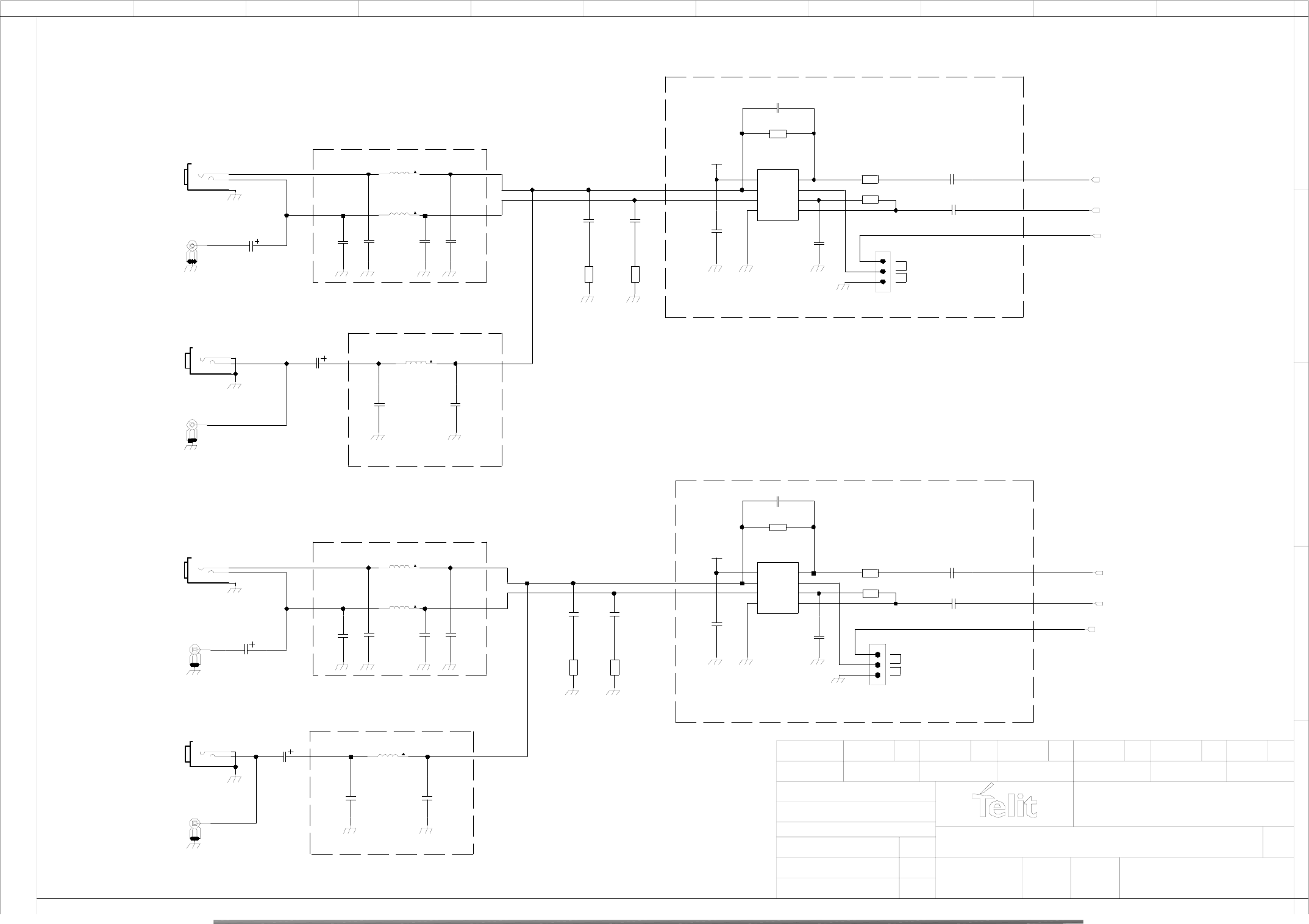
Reproduction forbidden without DAI Telecom written authorization – All Right reserved – Right of modification reserved page 61 of 69
FORBIDDENVIETATE
ALL RIGHTS RESERVED
RIPRODUZIONE E DIVULGAZIONE REPRODUCTION AND DISCLOSURE
TUTTI I DIRITTI RISERVATI
PROJECT A3
DESCRIPTION
DRAWING CODE
FORM
MODIFY
OF SHEETS
DATE
SHEET N.
VERIFIED
PROJECT
DRAWN
PATH /home/users/area
Mod. 067 rev.0 03/01 ANNOTATION
FILE NAME
B
C
D
E
A
Mobile Terminals S.p.A.
42 981 0713 1165
50V
0603
10pF
COG
C817
0603
15
5%
R806
50V
0603
39pF
COG
C808
GND
LQG18HN39NJ00
LQG18
39nH
L804
GND
16V
CONT-E
220uF
C820
GND
J01001A1944
SO806
1
IO
2
3
4
5
LQG18HN39NJ00
LQG18
39nH
L801
50V
0603
39pF
COG
C810
J01001A1944
SO807
1
IO
2
3
4
5
GND
GND
GND
LM4862M
U802
6VDD
2
BYPASS
3
IN+
8VC2
1
SHUTDOWN
7GND
4
IN-
5VC1
6.3V
0603
1uF
X5R
C818
GND
GND
+3.7V
1215061-03F
PL804
2
1
3
50V
0603
10pF
COG
C803
GND
LQG18HN39NJ00
LQG18
39nH
L803
EAR_HF-
004:3D;009:11C
1215061-03F
PL803
2
1
3
0603
1nF
C807
50V
X7R
50V
0603
1nF
X7R
C809
GND
GND
0603
15
5%
R807
50V
0603
39pF
COG
C812
50V
0603
39pF
COG
C811 16V
0603
100nF
Y5V
C825
MUTE
005:5B;008:10D;009:11C
GND
0603
15
5%
R809
0603
15
5%
R810
GND
0603
1M
5%
R812
GND
J01001A1944
SO808
1
IO
2
3
4
5
6.3V
0603
1uF
X5R
C801
GND
GND
0603
56K
5%
R802
50V
0603
1nF
X7R
C815
LM4862M
U801
6VDD
2
BYPASS
3
IN+
8VC2
1
SHUTDOWN
7GND
4
IN-
5VC1
GND
EAR_HF+
004:3D;009:11B
EAR_MT+
004:3D;006:10E
0603
100K
5%
R803
GND
GND
16V
0603
100nF
Y5V
C826
16V
0603
100nF
Y5V
C821
16V
0603
100nF
Y5V
C802
50V
0603
39pF
COG
C804
EAR_MT-
004:3D;006:10D
GND
50V
0603
1nF
X7R
C813
GND
16V
0603
100nF
Y5V
C829
J01001A1944
SO805
1
IO
2
3
4
5
LGY6502-0600
LGY650X
SO801
3
2
1
GND
GND
16V
0603
100nF
Y5V
C828
GND
GND
0603
56K
5%
R801
MUTE
005:5B;008:10B;009:11C
GND
0603
1M
5%
R811
GND
LQG18HN39NJ00
LQG18
39nH
L806
16V
0603
100nF
Y5V
C830
LQG18HN39NJ00
LQG18
39nH
L805
16V
CONT-E
220uF
C823
16V
0603
100nF
Y5V
C822
50V
0603
1nF
X7R
C806
+3.7V
16V
0603
100nF
Y5V
C827
16V
CONT-E
220uF
C819
GND
50V
0603
1nF
X7R
C814
LGY6502-0600
LGY650X
SO803
3
2
1
GND
16V
CONT-E
220uF
C824
LGY6502-0600
LGY650X
SO802
3
2
1
GND
GND
0603
56K
R804
5%
LQG18HN39NJ00
LQG18
39nH
L802
16V
0603
100nF
Y5V
C816
50V
0603
39pF
COG
C805
LGY6502-0600
LGY650X
SO804
3
2
1
GND
cs944b.cir
81 0
INTERNAL EAR (HANDSET)/ EXTERNAL EAR (HANDSFREE)
0208
EVK for GM862/S1
30208SE10944b
BRIDGED
NOISE FILTERING
INTERNAL EAR
NOISE FILTERING
SINGLE ENDED
INTERNAL EAR
BRIDGED
EXTERNAL EAR
SINGLE ENDED
NOISE FILTERING
EXTERNAL EAR
NOISE FILTERING
INTERNAL EAR AMPLIFIER +6dB
LOW VOLTAGE EXTERNAL EAR AMPLIFIER +12dB
EXT_EAR+
EXT_EAR-
INT_EAR+
INT_EAR-
MUTE CONTROLLED
ALWAYS ON
AMPLI POWER CONTROL
ALWAYS ON
AMPLI POWER CONTROL
MUTE CONTROLLED
Serdi M. 041201
041201
301101
Locatelli M.
Deperini F.
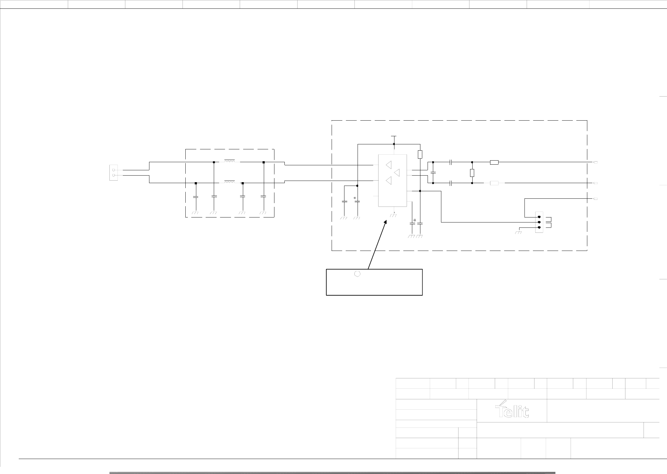
Reproduction forbidden without DAI Telecom written authorization – All Right reserved – Right of modification reserved page 62 of 69
0603
10K
5%
R904
TDA8943SF-N1
SOT110-1
U901
9NC
7
MODE
2
VCC
8
GND
4
IN+
3OUT+
6
SVR
1OUT-
5
IN-
50V
0603
1nF
X7R
C905
noMount=YES
GND
EAR_HF+
004:3D;008:10D
GND
MUTE
005:5B;008:10B;008:10D
GND
+12V
BLM21
220
L902
50V
0603
39pF
COG
C904
noMount=YES
35V
18
1000uF
C901
GND
BLM21
220
L901
0603
56K
5%
R901
noMount=YES
FCMM0502
SO901
2
1
16V
0603
100nF
Y5V
C912
1215061-03F
PL901
2
1
3
FORBIDDENVIETATE
ALL RIGHTS RESERVED
RIPRODUZIONE E DIVULGAZIONE REPRODUCTION AND DISCLOSURE
TUTTI I DIRITTI RISERVATI
PROJECT A3
DESCRIPTION
DRAWING CODE
FORM
MODIFY
OF SHEETS
DATE
SHEET N.
VERIFIED
PROJECT
DRAWN
PATH /home/users/area
Mod. 067 rev.0 03/01 ANNOTATION
FILE NAME
B
C
D
E
A
Mobile Terminals S.p.A.
42 981 0713 1165
50V
0603
39pF
COG
C903
noMount=YES
16V
0603
100nF
Y5V
C911
GND
16V
0603
100nF
Y5V
C902
GND
16V
0603
100nF
Y5V
C908
0603
10K
5%
R903
GND
0603
15K
5%
R902
35V
CONT-E
10uF
C910
50V
0603
1nF
X7R
C906
noMount=YES
GND
GND
EAR_HF-
004:3D;008:10D
GND
50V
0603
1.5nF
X7R
C913
HIGH POWER EXTERNAL EAR (HANDSFREE)
0208
EXTERNAL EAR
NOISE FILTERING
cs944b.cir
30208SE10944b9
HIGH POWER BRIDGED
10
EVK for GM862/S1
HIGH POWER EXT EAR AMPLIFIER (6W)
NOTE:
Heat Sink may be required
!
Refer to chip datasheet
MUTE CONTROLLED
ALWAYS ON
AMPLI POWER CONTROL
MIN 8 OHM
Serdi M. 041201
041201
301101
Locatelli M.
Deperini F.
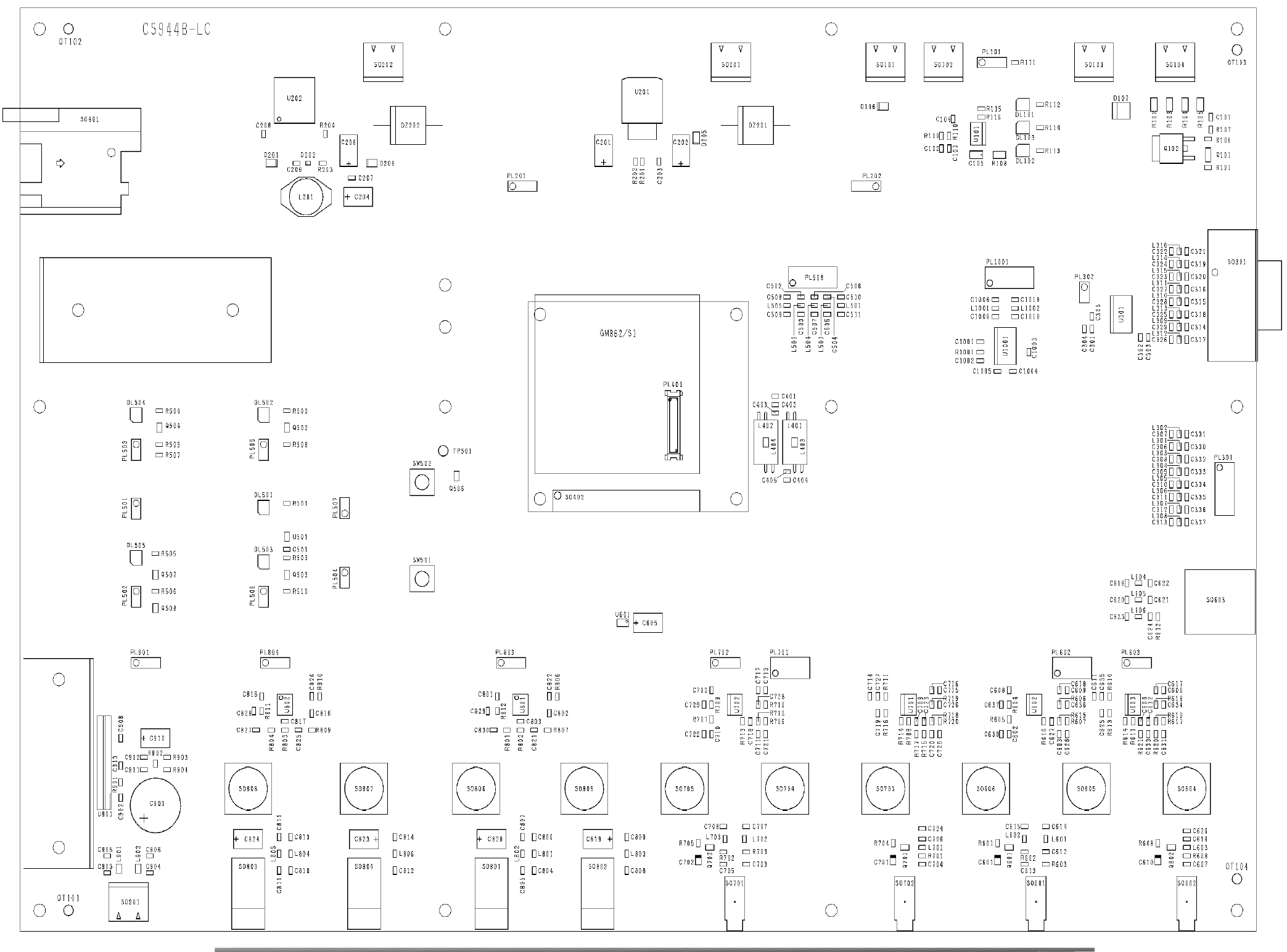
Reproduction forbidden without DAI Telecom written authorization – All Right reserved – Right of modification reserved page 63 of 69
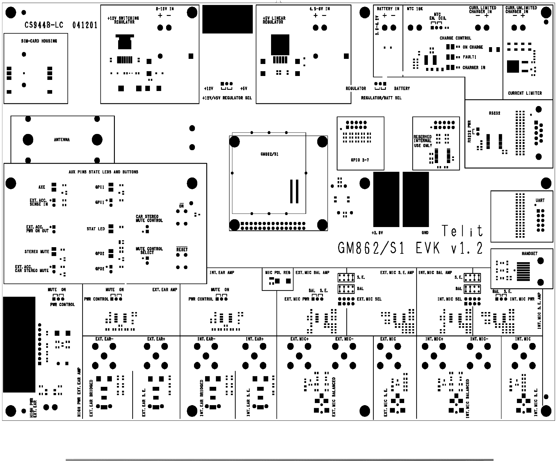
Reproduction forbidden without DAI Telecom written authorization – All Right reserved – Right of modification reserved page 64 of 69

Telit GM862-QUAD Hardware User guide
1vv0300692, Rev. ISSUE#0, - 04/10/2005
Reproduction forbidden without DAI Telecom written authorization – All Right reserved – Right of modification reserved
page 65 of 69
11 Annex B - Camera EVB schematics
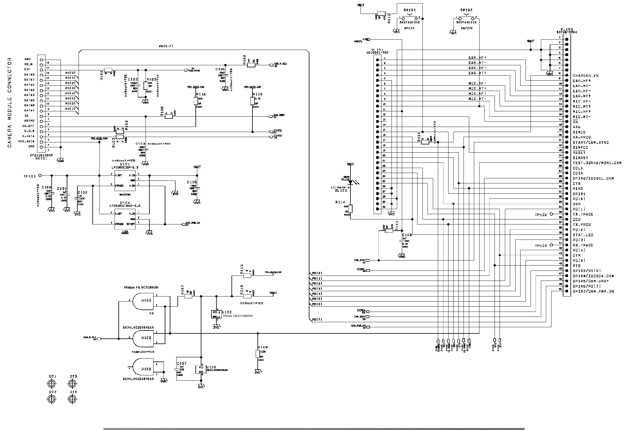
Reproduction forbidden without DAI Telecom written authorization – All Right reserved – Right of modification reserved page 66 of 69
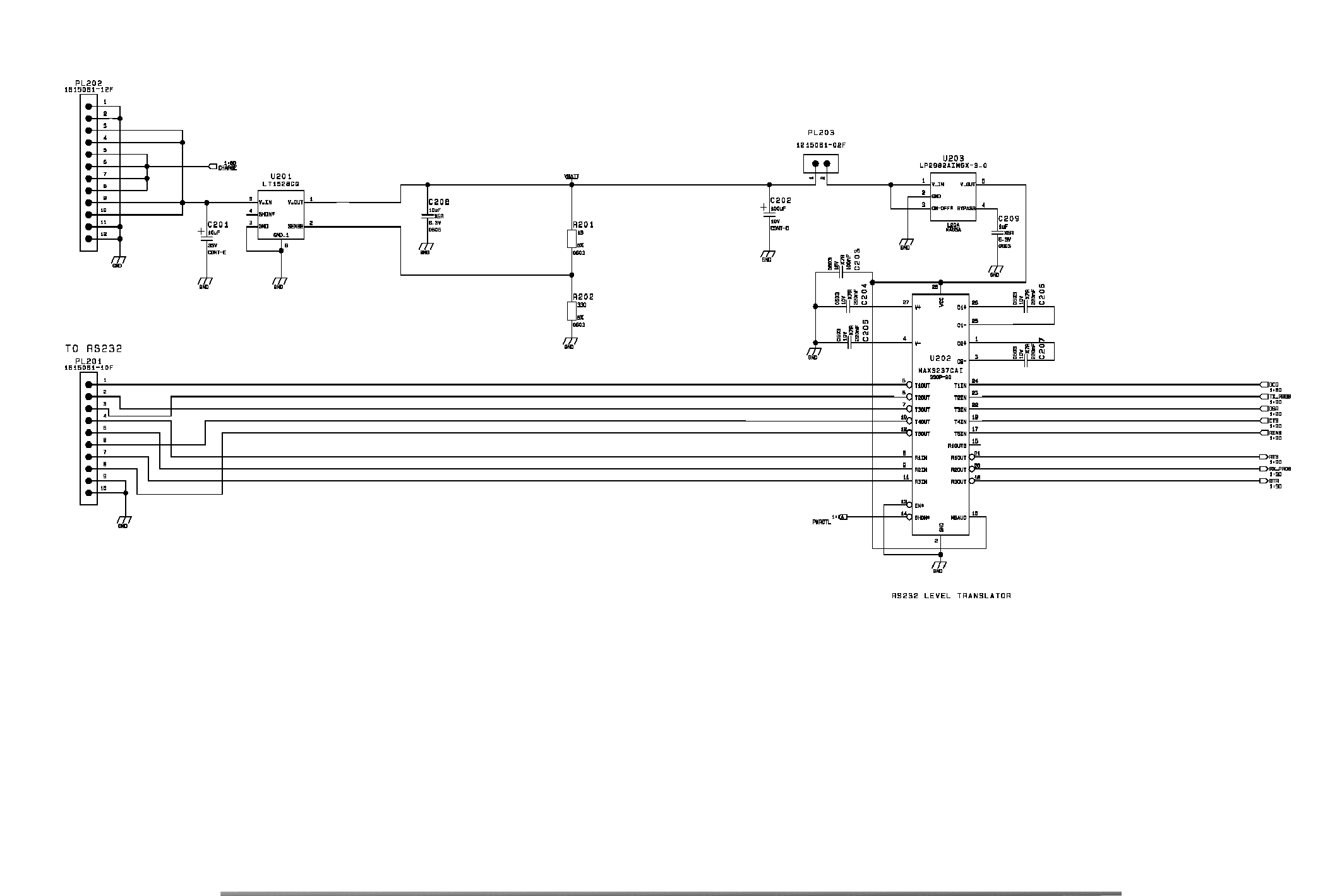
Reproduction forbidden without DAI Telecom written authorization – All Right reserved – Right of modification reserved page 67 of 69
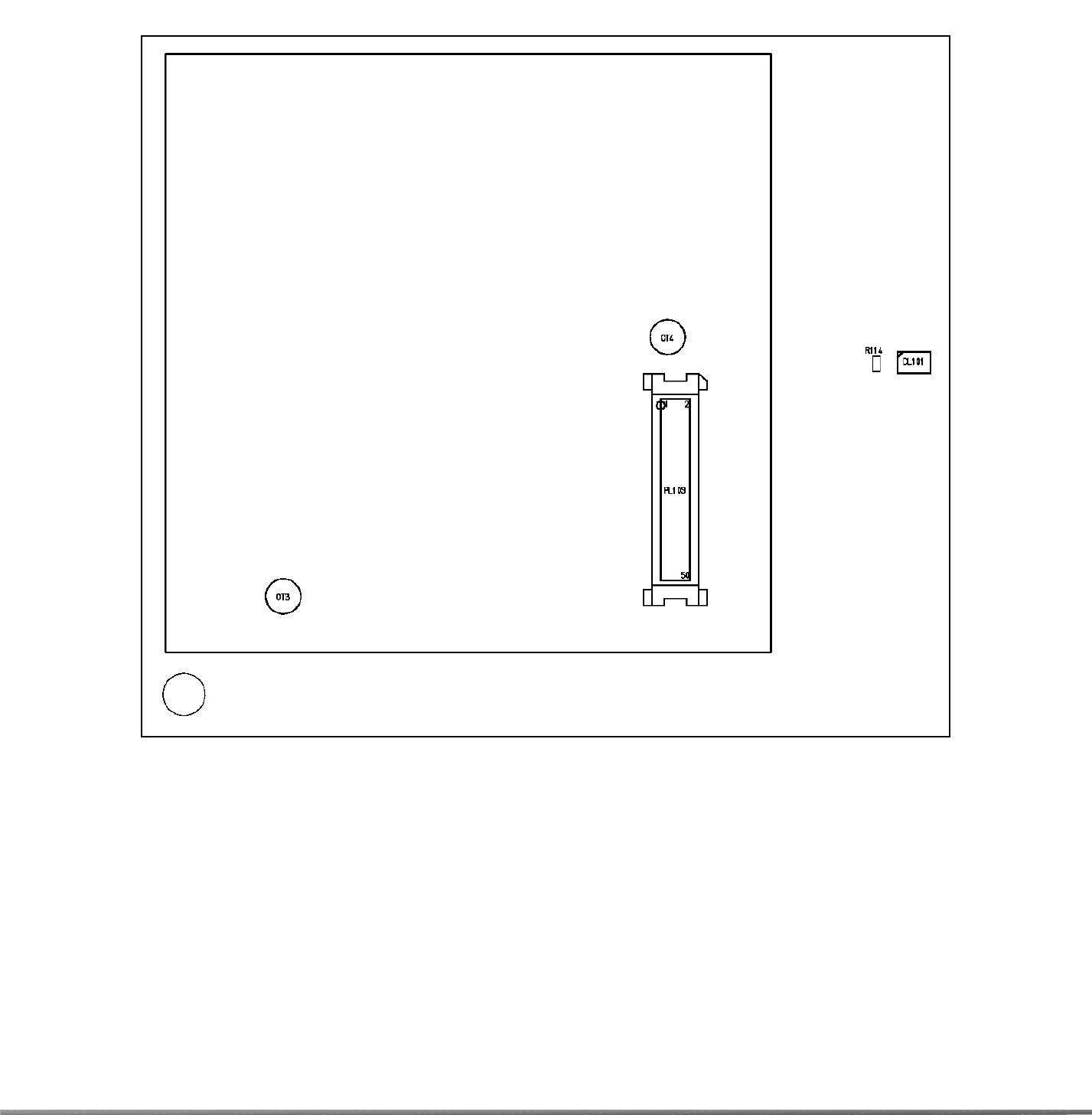
Reproduction forbidden without DAI Telecom written authorization – All Right reserved – Right of modification reserved page 68 of 69
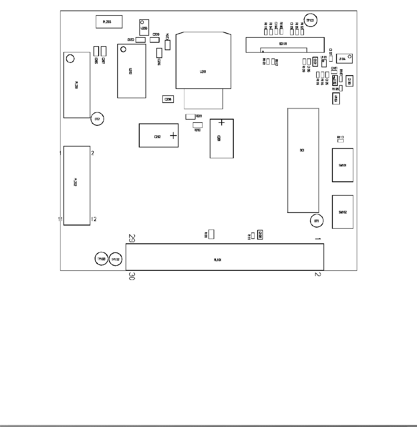
Reproduction forbidden without DAI Telecom written authorization – All Right reserved – Right of modification reserved page 69 of 69