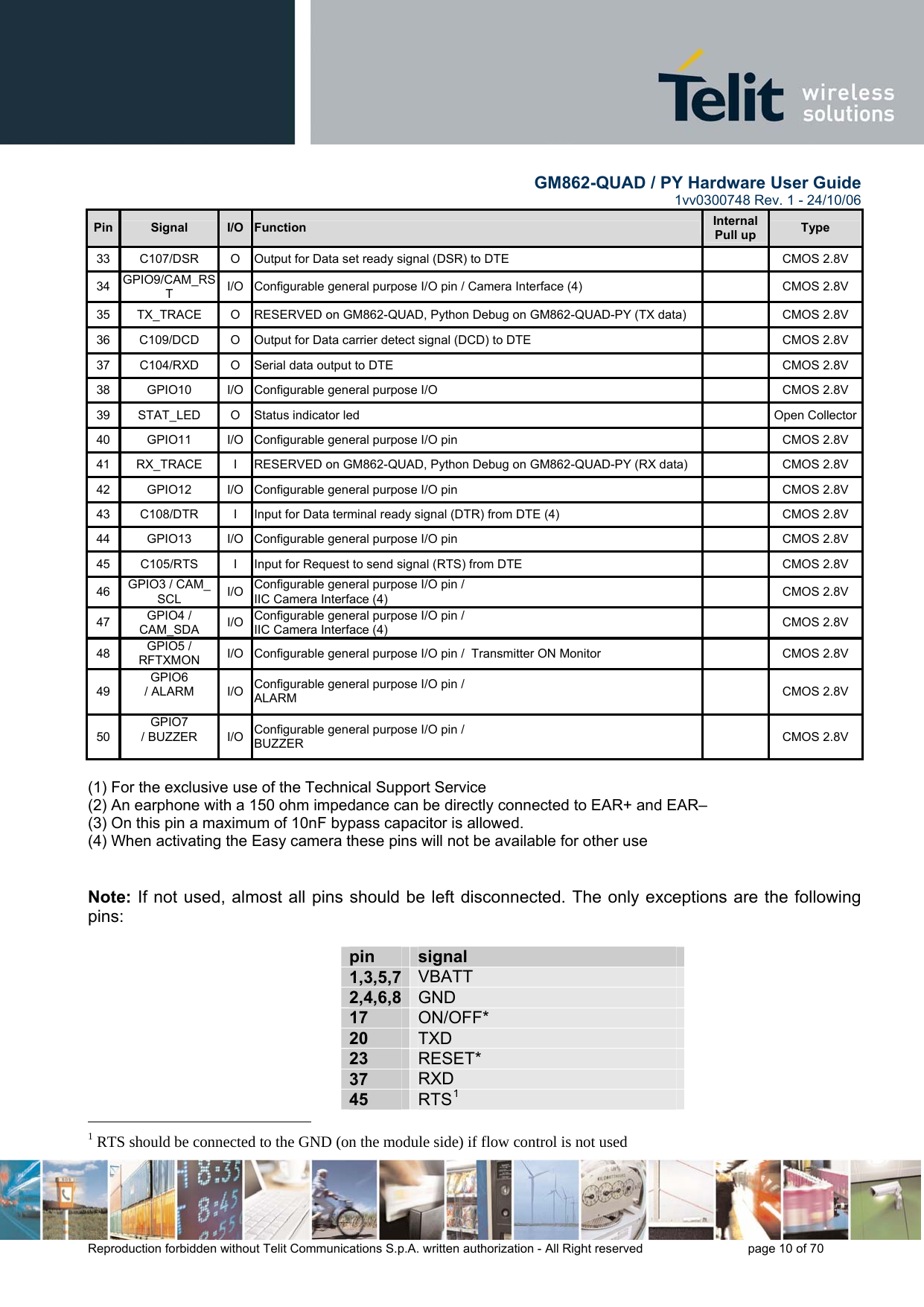
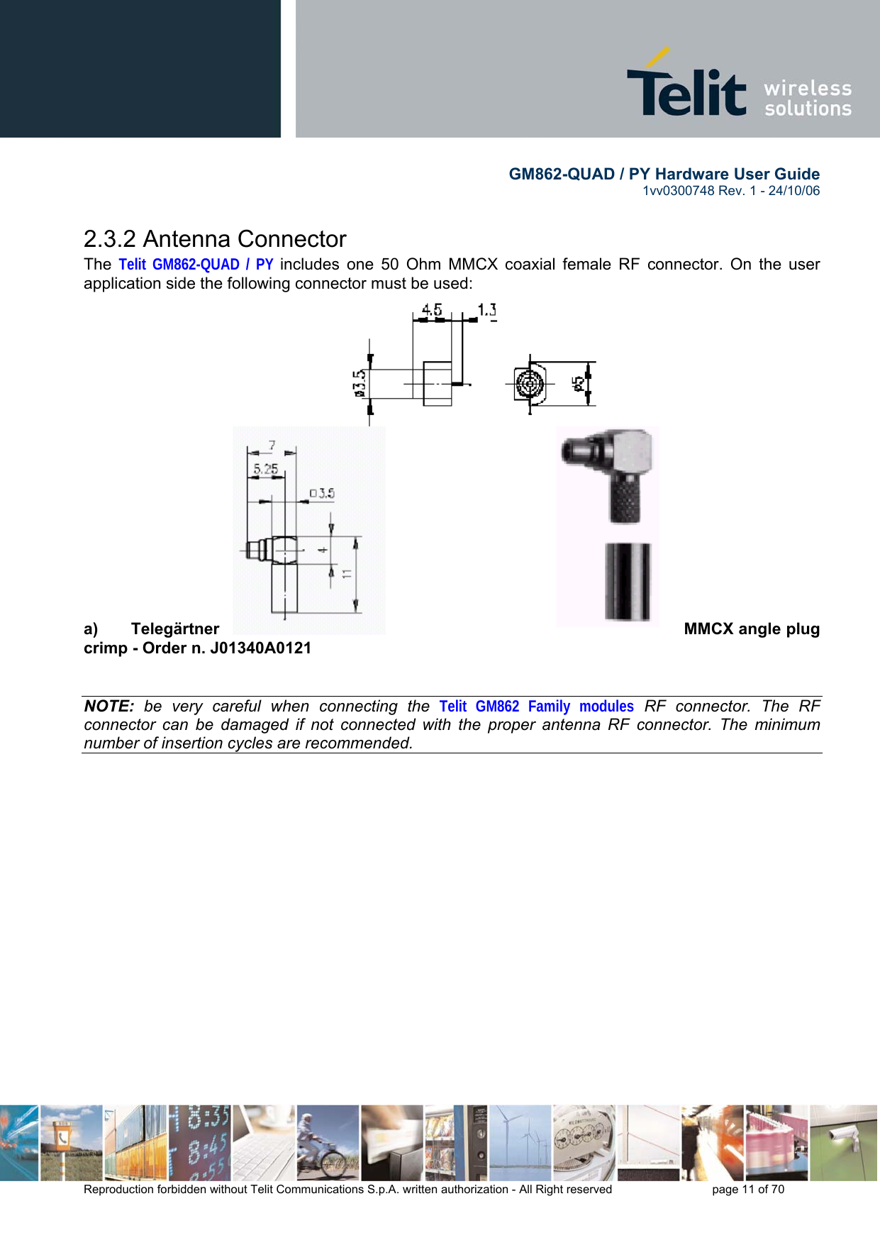
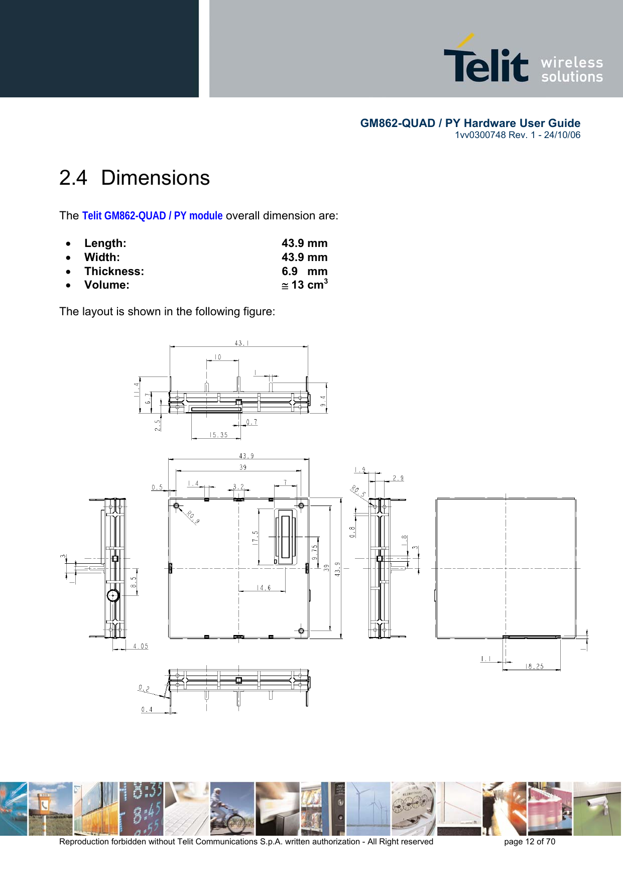
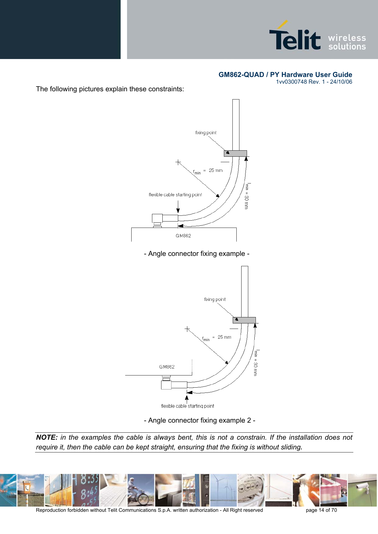
Telit Communications S p A GM862L Quad-Band GSM/GPRS module User Manual GM862 QUAD PY Hardware User Guide
Telit Communications S.p.A. Quad-Band GSM/GPRS module GM862 QUAD PY Hardware User Guide
UserManual.wiki
>
Telit Communications S p A
>
GM862L User Manual
Users Manual
Navigation menu
Upload a User Manual
Namespaces
Wiki Guide
HTML
PDF
Info
Views
User Manual
Discussion / Help
Navigation


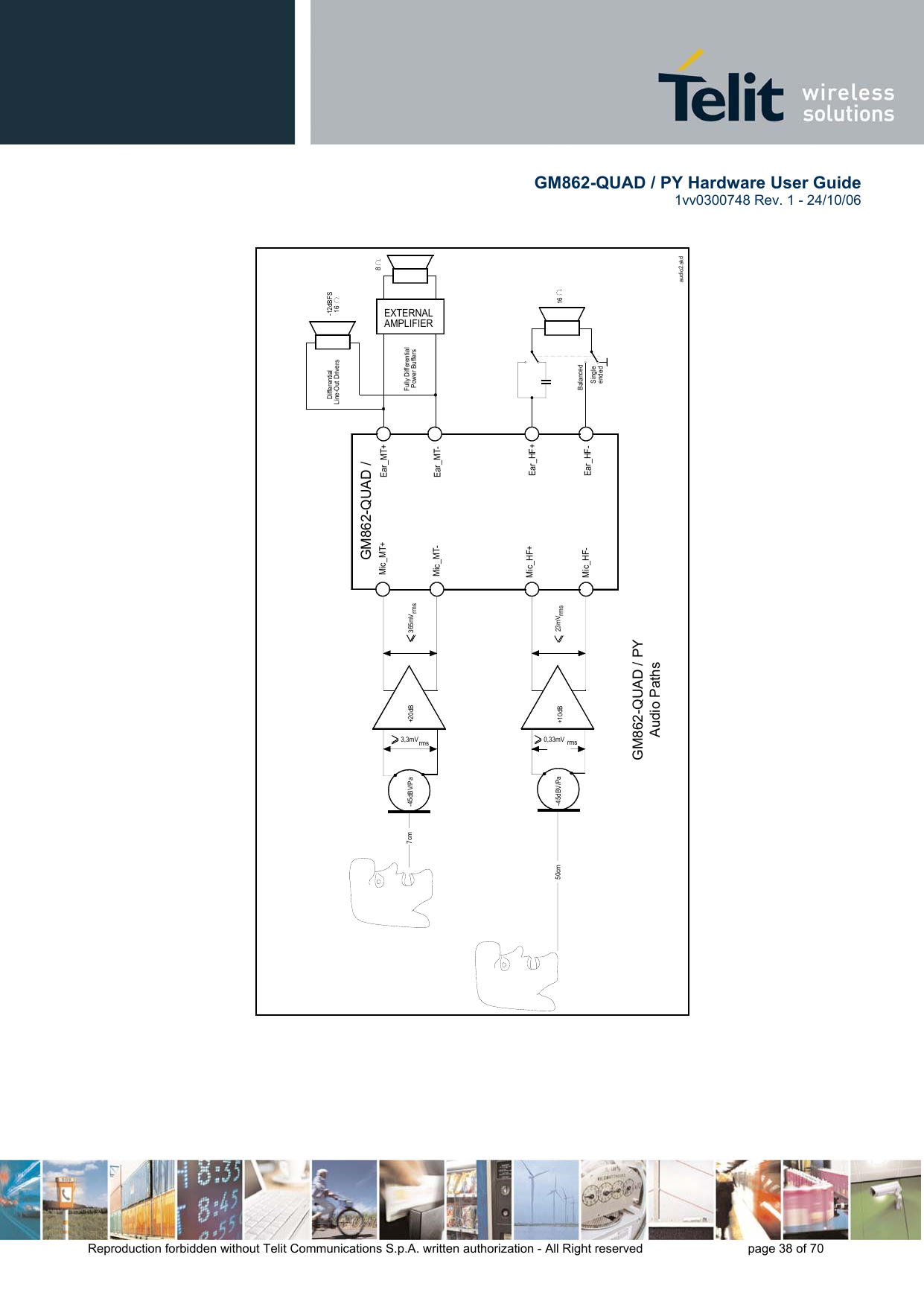
![GM862-QUAD / PY Hardware User Guide 1vv0300748 Rev. 1 - 24/10/06 Reproduction forbidden without Telit Communications S.p.A. written authorization - All Right reserved page 40 of 70 TIP: definition of the nominal sensitivity of the microphone lines . The nominal sensitivity of the microphone lines indicates the voltage level on the GM862-QUAD / PY pins present during "normal spoken" conditions. For a handset , the "normal spoken” conditions take place when the talker mouth is 7cm far from the microphone ; under these conditions the voice will produce an acoustic pressure of -4,7dBPa @1kHz on the microphone membrane . TIP: electrical equivalent signal and operating voice levels . At "normal spoken" conditions, a microphone having the suggested nominal sensitivity of -45dBVrms/Pa , will produce the electrical equivalent signal : that means : During a call , this level varies according to the volume of the talker voice; usually the following rough thumb rule for the dynamic range may be used : 1) the talker is screaming . This is the strongest voice level condition: the signal increases by +20dB ; 2) the talker is whispering. This is the lowest voice level condition: the voice level decreases by –50dB . These changes must be considered for designing the external microphone amplifier. TIP: example of external microphone amplifier calculation . Let’s suppose to use the 1stdifferential microphone path .In this case the maximum differential input voltage to “Mic_MT” lines is 365mVrms(1,03Vpp) corresponding to –8,76dBV. Now we can calculate the maximum voltage gain of an external microphone amplifier GA: ()[]dBVGdBMicLevel A76,820 −=++ []76,8207,49 −=++− AG AG−=+− 209,40 dBGA94,20= you can set GA= +20dB to use standard resistor values . MicLevel = ( -45) + (-4.7) = -49.7 dBVrmsMicVoltage = 10 ( -49.7 / 20 ) = 3.3* 10 -3 Vrms](https://usermanual.wiki/Telit-Communications-S-p-A/GM862L/User-Guide-732791-Page-40.png)
![GM862-QUAD / PY Hardware User Guide 1vv0300748 Rev. 1 - 24/10/06 Reproduction forbidden without Telit Communications S.p.A. written authorization - All Right reserved page 47 of 70 The buffer gain is given by the formula: 607606605604RRRRGain == The C636 and C637 capacitors are placed in order to cut off the gain at higher frequencies than the transmitted GSM band, the cutoff frequency (-3dB) should be 3500Hz in order to have -1dB at 3kHz. The cutoff frequency is given by the formula: 636*606*21637*604*21.CRCRfreqππ== [Hz] TIP: example of calculation. Let's assume you have a microphone with a sensitivity of -45 dBVrms/Pa and you want to use it in 1st differential microphone path (“Mic_MT” inputs) in "normal spoken" conditions at acoustic pressure of -4.7dBPa. As reported at page 33 , the electrical level output from the microphone will be : corresponding to: When the talker is screaming , we will have a signal of 330 mVrms on the “Mic_MT “ inputs due to a 20dB higher Mic Level (see TIP 1) with a buffer gain GA : GA =20 log (AmplifierOutput / MicVoltage) =20 log (330 * 10 -3 )/( 33 * 10 -3 ) = 20 log 10=20dB The corresponding values for the resistors on the buffer could be ( if we keep the input resistance 10kΩ ) R604 = R606 = gain* R607= gain* R605 = 10* 15 = 150 kΩ The commercial values of 150kΩ & 15kΩ are then chosen. As a consequence the values of the capacitors C636 and C637 shall be: C636=C637= 1/ (2π*4000*R606)= 265 *10 -12 F A commercial value of 270pF gives a cutoff frequency of 3931Hz with an errorless than 1,8% . MicLevel = ( -45) + (-4.7) = -49.7 dBVrms MicVoltage = 10 ( -49.7 / 20 ) = 3.3* 10 -3 Vrms](https://usermanual.wiki/Telit-Communications-S-p-A/GM862L/User-Guide-732791-Page-47.png)
![GM862-QUAD / PY Hardware User Guide 1vv0300748 Rev. 1 - 24/10/06 Reproduction forbidden without Telit Communications S.p.A. written authorization - All Right reserved page 48 of 70 6.5.2 Buffered Unbalanced (Single Ended) Microphone . The above schematic can be used for a single ended (buffered unbalanced) microphone ; the required biasing circuitry is not included. Note also that the capacitor C3 is not needed . The gains of the two amplifiers are given by the formulas : ()7207191buffer invertingnot RRGain += ()708711buffer inverting RRGain = Assigning half of overall gain to each amplifier, you will obtain the requested gain because of doubling the microphone signal path; in fact by the use of two amplifiers (the upper as “inverting” and the lower as “not inverting”configuration ) we obtain an additional +6dB gain (2 times) . Remember : the “not inverting “ amplifier section gain shall not be less than 1 . Like for the balanced buffered microphone , the amplifier overall gain can be modify changing the value of resistor R719/R720 and R711 and as a consequence the capacitors C726 and C727. It is advisable to change R708 only if you have difficulty to find a commercial value for R711 ; in this case change R708 as little as possible . The -3dB bandwidth is given by the approximated formula (considering C725 >> C726): 727*711*21726*719*21.CRCRfreqππ== [Hz] 2,7nF 6,8nF](https://usermanual.wiki/Telit-Communications-S-p-A/GM862L/User-Guide-732791-Page-48.png)
![GM862-QUAD / PY Hardware User Guide 1vv0300748 Rev. 1 - 24/10/06 Reproduction forbidden without Telit Communications S.p.A. written authorization - All Right reserved page 55 of 70 The resulting gain and high pass cut can be obtained with the formula: 23RRGain = 4*3*21.CRfreqπ= [Hz] And an example of internal Ear amplifier could be : Some amplifier require a low impedance load at high frequency in order to avoid auto oscillation, this can be made with a capacitor (100nF) in series with a resistor (15Ω). When designing your application, remember to provide an adequate bypass capacitor to the amplifier and place it close to the power input pin of the IC, keeping the traces as short as possible. 7.5 Hands-Free Earphone (Low Power) Design The same design considerations made for the handset are valid for the hands-free earphone. +12dBGM862-QUAD / PY](https://usermanual.wiki/Telit-Communications-S-p-A/GM862L/User-Guide-732791-Page-55.png)
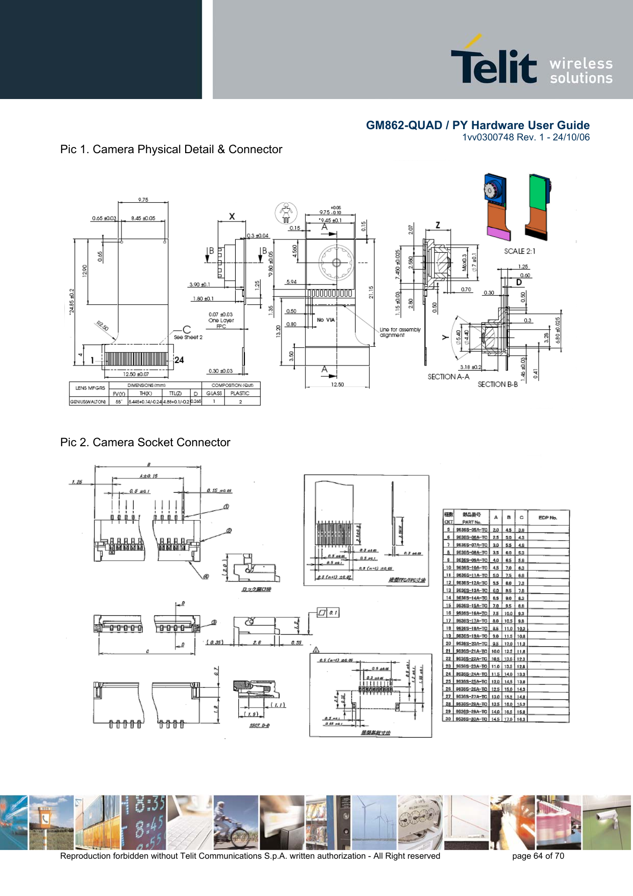
![GM862-QUAD / PY Hardware User Guide 1vv0300748 Rev. 1 - 24/10/06 Reproduction forbidden without Telit Communications S.p.A. written authorization - All Right reserved page 66 of 70 10.1.4 Block Diagram for supported camera DVDD is an external power supply of 2.8V, controlled or gated by pin CAM_PWR_ON. 1 2 3 4 5 6 7 8 9 10 11 12 13 14 15 16 17 18 19 20 21 22 23 24 GND AVDD CAM_CLK GND DVDD IICSDA_CAM GND GND PD[1] PD[0] PD[6] CAM_CLK DVDD AVDD GND CAMERA TRANSCHIP MON1_CAM](https://usermanual.wiki/Telit-Communications-S-p-A/GM862L/User-Guide-732791-Page-66.png)