Telit Communications S p A HE910NA 2G/3.5G module, HE910-NAG; HE910-NAR; HE910-NAD User Manual HE910 Hardware User Guide
Telit Communications S.p.A. 2G/3.5G module, HE910-NAG; HE910-NAR; HE910-NAD HE910 Hardware User Guide
User_Guide_r18

HE910 Hardware User Guide
1vv0300925 Rev.18 – 15-06-2012
Reproduction forbidden without Telit Communications S.p.A. written authorization - All Rights Reserved page 2 of 91
PRODUCT
HE910
HE910-GA
HE910-D
HE910-EUR
HE910-EUD
HE910-EUG
HE910-NAR
HE910-NAD
HE910-NAG

HE910 Hardware User Guide
1vv0300925 Rev.18 – 15-06-2012
Reproduction forbidden without Telit Communications S.p.A. written authorization - All Rights Reserved page 3 of 91
DISCLAIMER
The information contained in this document is the proprietary information of Telit
Communications S.p.A. and its affiliates (“TELIT”). The contents are confidential and any
disclosure to persons other than the officers, employees, agents or subcontractors of the owner
or licensee of this document, without the prior written consent of Telit, is strictly prohibited.
Telit makes every effort to ensure the quality of the information it makes available.
Notwithstanding the foregoing, Telit does not make any warranty as to the information
contained herein, and does not accept any liability for any injury, loss or damage of any kind
incurred by use of or reliance upon the information.
Telit disclaims any and all responsibility for the application of the devices characterized in this
document, and notes that the application of the device must comply with the safety standards of
the applicable country, and where applicable, with the relevant wiring rules.
Telit reserves the right to make modifications, additions and deletions to this document due to
typographical errors, inaccurate information, or improvements to programs and/or equipment at
any time and without notice. Such changes will, nevertheless be incorporated into new editions
of this application note.
All rights reserved.
© 2011, 2012 Telit Communications S.p.A.

HE910 Hardware User Guide
1vv0300925 Rev.18 – 15-06-2012
Reproduction forbidden without Telit Communications S.p.A. written authorization - All Rights Reserved page 4 of 91
1 INTRODUCTION ......................................................................................................................................................... 7
1.1 SCOPE ................................................................................................................................................................................ 7
1.2 AUDIENCE ........................................................................................................................................................................... 7
1.3 CONTACT INFORMATION, SUPPORT .......................................................................................................................................... 7
1.4 DOCUMENT ORGANIZATION ................................................................................................................................................... 8
1.5 TEXT CONVENTIONS .............................................................................................................................................................. 9
1.6 RELATED DOCUMENTS ........................................................................................................................................................... 9
1.7 DOCUMENT HISTORY .......................................................................................................................................................... 10
2 OVERVIEW .............................................................................................................................................................. 11
3 HE910 MODULE CONNECTIONS ............................................................................................................................... 12
3.1 PIN-OUT ......................................................................................................................................................................... 12
3.1.1 LGA Pads Layout (HE910 and HE910-GA) .............................................................................................................. 18
3.1.2 LGA Pads Layout (HE910-D) ................................................................................................................................... 19
3.1.3 LGA Pads Layout (HE910-EUx and HE910-NAx) ..................................................................................................... 20
3.1.4 LGA Pads Layout (HE910-EUG and HE910-NAG) .................................................................................................... 21
4 HARDWARE COMMANDS ........................................................................................................................................ 22
4.1 TURNING ON THE HE910 ................................................................................................................................................... 22
4.2 TURNING OFF THE HE910 .................................................................................................................................................. 27
4.3 HE910 UNCONDITIONAL SHUTDOWN .................................................................................................................................... 29
4.4 HE910 RESET .................................................................................................................................................................. 32
5 POWER SUPPLY ....................................................................................................................................................... 35
5.1 POWER SUPPLY REQUIREMENTS ............................................................................................................................................ 35
5.2 POWER CONSUMPTION ....................................................................................................................................................... 36
5.3 GENERAL DESIGN RULES ...................................................................................................................................................... 37
5.3.1 Electrical Design Guidelines ................................................................................................................................... 37
5.3.2 Thermal Design Guidelines ..................................................................................................................................... 41
5.3.3 Power Supply PCB layout Guidelines ...................................................................................................................... 42
6 GSM/WCDMA RADIO SECTION ............................................................................................................................... 43
6.1 HE910 PRODUCT VARIANTS ................................................................................................................................................ 43
6.2 TX OUTPUT POWER ............................................................................................................................................................ 43
6.3 SENSITIVITY ....................................................................................................................................................................... 44
6.4 GSM/WCDMA ANTENNA REQUIREMENTS ............................................................................................................................ 44
6.5 GSM/WCDMA - PCB LINE GUIDELINES ................................................................................................................................ 45
6.6 GSM/WCDMA ANTENNA - INSTALLATION GUIDELINES ........................................................................................................... 46
6.7 ANTENNA DIVERSITY REQUIREMENTS ..................................................................................................................................... 47
7 GPS RECEIVER .......................................................................................................................................................... 48
7.1 GPS PERFORMANCES .......................................................................................................................................................... 48
7.2 GPS SIGNALS PINOUT ......................................................................................................................................................... 49
7.3 RF FRONT END DESIGN ....................................................................................................................................................... 49
7.3.1 RF Signal Requirements .......................................................................................................................................... 49
7.3.2 GPS Antenna Polarization ...................................................................................................................................... 50

HE910 Hardware User Guide
1vv0300925 Rev.18 – 15-06-2012
Reproduction forbidden without Telit Communications S.p.A. written authorization - All Rights Reserved page 5 of 91
7.3.3 GPS Antenna Gain .................................................................................................................................................. 51
7.3.4 Active versus Passive Antenna ............................................................................................................................... 51
7.3.5 GPS Antenna - PCB Line Guidelines ........................................................................................................................ 52
7.3.6 RF Trace Losses....................................................................................................................................................... 52
7.3.7 Implications of the Pre-select SAW Filter ............................................................................................................... 53
7.3.8 External LNA Gain and Noise Figure....................................................................................................................... 53
7.3.9 Powering the External LNA (active antenna) ......................................................................................................... 53
7.3.10 External LNA Enable ............................................................................................................................................. 54
7.3.11 Shielding ............................................................................................................................................................... 55
7.3.12 GPS Antenna - Installation ................................................................................................................................... 55
8 LOGIC LEVEL SPECIFICATIONS .................................................................................................................................. 56
8.1 RESET SIGNAL .................................................................................................................................................................... 57
9 USB PORT ................................................................................................................................................................ 58
9.1 USB 2.0 HS ...................................................................................................................................................................... 58
10 SPI PORT ................................................................................................................................................................. 59
10.1 SPI CONNECTIONS ............................................................................................................................................................ 60
11 SERIAL PORTS .......................................................................................................................................................... 61
11.1 MODEM SERIAL PORT 1 (USIF0) ................................................................................................................................... 62
11.2 MODEM SERIAL PORT 2 (USIF1) ................................................................................................................................... 64
11.3 RS232 LEVEL TRANSLATION ................................................................................................................................................ 65
12 AUDIO SECTION OVERVIEW .................................................................................................................................... 67
12.1 ELECTRICAL CHARACTERISTICS ............................................................................................................................................. 67
12.1.1 CODEC Examples .................................................................................................................................................. 67
13 GENERAL PURPOSE I/O ........................................................................................................................................... 68
13.1 GPIO LOGIC LEVELS .......................................................................................................................................................... 69
13.2 USING A GPIO PAD AS INPUT ........................................................................................................................................... 70
13.3 USING A GPIO PAD AS OUTPUT ........................................................................................................................................ 70
13.4 INDICATION OF NETWORK SERVICE AVAILABILITY ..................................................................................................................... 71
13.5 RTC BYPASS OUT ............................................................................................................................................................. 72
13.6 EXTERNAL SIM HOLDER IMPLEMENTATION ........................................................................................................................... 72
13.7 VAUX POWER OUTPUT ..................................................................................................................................................... 72
13.8 ADC CONVERTER ............................................................................................................................................................. 73
13.8.1 Description ........................................................................................................................................................... 73
13.8.2 Using ADC Converter ............................................................................................................................................ 73
14 MOUNTING THE HE910 ON THE APPLICATION ........................................................................................................ 74
14.1 GENERAL ........................................................................................................................................................................ 74
14.2 MODULE FINISHING & DIMENSIONS ..................................................................................................................................... 74
14.3 RECOMMENDED FOOT PRINT FOR THE APPLICATION ................................................................................................................. 76
14.4 STENCIL .......................................................................................................................................................................... 77
14.5 PCB PAD DESIGN .............................................................................................................................................................. 77
14.6 PCB PAD DIMENSIONS ....................................................................................................................................................... 78
14.7 SOLDER PASTE .................................................................................................................................................................. 80

HE910 Hardware User Guide
1vv0300925 Rev.18 – 15-06-2012
Reproduction forbidden without Telit Communications S.p.A. written authorization - All Rights Reserved page 6 of 91
14.7.1 HE910 Solder reflow ............................................................................................................................................. 80
14.8 PACKING SYSTEM .............................................................................................................................................................. 82
14.9 MOISTURE SENSITIVITY ...................................................................................................................................................... 84
15 SAFETY RECOMMANDATIONS ................................................................................................................................. 85
16 CONFORMITY ASSESSMENT ISSUES ......................................................................................................................... 86
16.1 1999/5/EC DIRECTIVE ..................................................................................................................................................... 86
16.2 FCC/IC REGULATORY NOTICES ............................................................................................................................................ 90

HE910 Hardware User Guide
1vv0300925 Rev.18 – 15-06-2012
Reproduction forbidden without Telit Communications S.p.A. written authorization - All Rights Reserved page 7 of 91
The aim of this document is the description of some hardware solutions useful for developing a
product with the Telit HE910 module.
This document is intended for Telit customers, who are integrators, about to implement their
applications using our HE910 modules.
For general contact, technical support, to report documentation errors and to order manuals,
contact Telit’s Technical Support Center (TTSC) at:
TS-EMEA@telit.com
TS-NORTHAMERICA@telit.com
TS-LATINAMERICA@telit.com
TS-APAC@telit.com
Alternatively, use:
http://www.telit.com/en/products/technical-support-center/contact.php
For detailed information about where you can buy the Telit modules or for recommendations on
accessories and components visit:
http://www.telit.com
To register for product news and announcements or for product questions contact Telit’s
Technical Support Center (TTSC).
Our aim is to make this guide as helpful as possible. Keep us informed of your comments and
suggestions for improvements.
Telit appreciates feedback from the users of our information.

HE910 Hardware User Guide
1vv0300925 Rev.18 – 15-06-2012
Reproduction forbidden without Telit Communications S.p.A. written authorization - All Rights Reserved page 8 of 91
This document contains the following chapters:
Chapter 1: “Introduction” provides a scope for this document, target audience, contact and
support information, and text conventions.
Chapter 2: “Overview” provides an overview of the document.
Chapter3: “HE910 Module Connections” deals with the pin out configuration and layout.
Chapter 4: “Hardware Commands” How to operate on the module via hardware.
Chapter 5: “Power supply” Power supply requirements and general design rules.
Chapter 6: “GSM/WCDMA Radio” The antenna connection and board layout design are the
most important parts in the full product design.
Chapter 7: “GPS Receiver” This section describes the GPS receiver.
Chapter 8: “Logic Level specifications” Specific values adopted in the implementation of logic
levels for this module.
Chapter 9: “USB Port” The USB port on the Telit HE910 is the core of the interface between the
module and OEM hardware
Chapter 10: “SPI port” Refers to the SPI port of the Telit HE910
Chapter 11: “Serial ports” Refers to the serial ports of the Telit HE910
Chapter 12: “Audio Section overview” Refers to the audio blocks of the Base Band Chip of the
HE910 Telit Modules.
Chapter 13: “General Purpose I/O” How the general purpose I/O pads can be configured.
Chapter 14: “Mounting the HE910 on the application board” Mechanical dimensions and
recommendations on how to mount the module on the user’s board.
Chapter 15: “Safety Recommendations” Information related to the Safety topics.
Chapter 16: “Conformity Assessment Issues” Information related to the Conformity
Assessments.
HE910 Hardware User Guide
1vv0300925 Rev.18 – 15-06-2012
Reproduction forbidden without Telit Communications S.p.A. written authorization - All Rights Reserved page 9 of 91
Danger – This information MUST be followed or catastrophic equipment failure or bodily
injury may occur.
Caution or Warning – Alerts the user to important points about integrating the module, if
these points are not followed, the module and end user equipment may fail or malfunction.
Tip or Information – Provides advice and suggestions that may be useful when integrating
the module.
All dates are in ISO 8601 format, i.e. YYYY-MM-DD.
HE910 Digital Voice Interface Application Note 80000NT10050A
HE910 SPI Port Application Note 80000NT10053A
HE910 Product description 80378ST10085a
SIM Holder Design Guides 80000NT10001a
AT Commands Reference Guide 80378ST10091A
Telit EVK2 User Guide 1vv0300704
HE910 Hardware User Guide
1vv0300925 Rev.18 – 15-06-2012
Reproduction forbidden without Telit Communications S.p.A. written authorization - All Rights Reserved page 10 of 91
R
Re
ev
vi
is
si
io
on
n
D
Da
at
te
e
C
Ch
ha
an
ng
ge
es
s
ISSUE#0
2011-03-31
Preliminary Version
ISSUE#1
2011-05-19
Updated pinout on UART1
ISSUE#2
2011-05-25
Update chapter 13
ISSUE#3
2011-07-25
Added DVI app note references; chapter 4.1
ISSUE#4
2011-07-29
Updated audio, on_off/reset and digital sections
ISSUE#5
2011-10-18
Added STAT_LED info, Updated SPI pinout
ISSUE#6
2011-12-22
- Pads A8, A9, D14, A14 now reserved
Power supply extended to 3.3 V
- par 4.3 renamed as “unconditional shutdown”
- USIF0 USIF1 names added to Main and AUX serial ports
- Updated IO logic levels
- Updated module’s mechanical drawing
- IO levels selection 1.8/1.2 removed (now only 1.8)
ISSUE#7
2012-01-16
Added HE910-GA and –D; added Conformity assessment chapter
ISSUE#8
2012-02-03
Chapter 5.1 updated
ISSUE#9
2012-02-07
Chapter 4.2 updated
ISSUE#10
2012-03-16
Added ADC in pinout description; added GPS specification; updated Chapter
13 and 14;
ISSUE#11
2012-03-26
Chapter 2.1, 2.1.2, 3.3, 5.4, 14.9
ISSUE#12
2012-03-27
Added HE910-EU and NA products
ISSUE#13
2012-03-28
Updated paragraph 14.9
ISSUE#14
2012-05-08
Added EUR, EUD, NAR, NAD variants; added Sensitivity and TX Power
Class specifications. Updated par 14.7.1 and 14.3
ISSUE#15
2012-05-30
Updated Chapter 16.2; 7.3.8
ISSUE#16
2012-06-06
Pin R13 renamed as HW_SHUTDOWN*, Pin P11 adeed in pinout as RESET*
ISSUE#17
2012-06-14
Updated RTT&E info on HE910-NAG, NAR, NAD
ISSUE#18
2012-06-15
Updated RTT&E info on HE910-NAG, NAR, NAD ; updated par 3.1;
HE910 Hardware User Guide
1vv0300925 Rev.18 – 15-06-2012
Reproduction forbidden without Telit Communications S.p.A. written authorization - All Rights Reserved page 11 of 91
The aim of this document is the description of some hardware solutions useful for developing a
product with the Telit HE910 module.
In this document all the basic functions of a mobile phone will be taken into account; for each
one of them a proper hardware solution will be suggested and eventually the wrong solutions
and common errors to be avoided will be evidenced. Obviously this document cannot embrace
the whole hardware solutions and products that may be designed. The wrong solutions to be
avoided shall be considered as mandatory, while the suggested hardware configurations shall not
be considered mandatory, instead the information given shall be used as a guide and a starting
point for properly developing your product with the Telit HE910 module. For further hardware
details that may not be explained in this document refer to the Telit HE910 Product Description
document where all the hardware information is reported.
NOTICE:
(EN) The integration of the GSM/GPRS/WCDMA HE910 cellular module within user application shall
be done according to the design rules described in this manual.
(IT) L’integrazione del modulo cellulare GSM/GPRS/WCDMA HE910 all’interno dell’applicazione
dell’utente dovrà rispettare le indicazioni progettuali descritte in questo manuale.
(DE) Die Integration des HE910 GSM/GPRS/WCDMA Mobilfunk-Moduls in ein Gerät muß gemäß der
in diesem Dokument beschriebenen Kunstruktionsregeln erfolgen.
(SL) Integracija GSM/GPRS/WCDMA HE910 modula v uporabniški aplikaciji bo morala upoštevati
projektna navodila, opisana v tem priročniku.
(SP) La utilización del modulo GSM/GPRS/WCDMA HE910 debe ser conforme a los usos para los
cuales ha sido deseñado descritos en este manual del usuario.
(FR) L’intégration du module cellulaire GSM/GPRS/WCDMA HE910 dans l’application de l’utilisateur
sera faite selon les règles de conception décrites dans ce manuel.
(HE)
The information presented in this document is believed to be accurate and reliable. However, no
responsibility is assumed by Telit Communications S.p.A. for its use, nor any infringement of patents or
other rights of third parties which may result from its use. No license is granted by implication or
otherwise under any patent rights of Telit Communications S.p.A. other than for circuitry embodied in
Telit products. This document is subject to change without notice.
HE910
HE910 Hardware User Guide
1vv0300925 Rev.18 – 15-06-2012
Reproduction forbidden without Telit Communications S.p.A. written authorization - All Rights Reserved page 12 of 91
PAD
Signal
I/O
Function
Type
COMMENT
USB HS 2.0 COMMUNICATION PORT
B15
USB_D+
I/O
USB differential Data (+)
C15
USB_D-
I/O
USB differential Data (-)
A13
VUSB
I
Power sense for the internal USB
transceiver.
Asynchronous Serial Port (USIF0) - Prog. / Data + HW Flow Control
N15
C103/TXD
I
Serial data input from DTE
CMOS 1.8V
M15
C104/RXD
O
Serial data output to DTE
CMOS 1.8V
M14
C108/DTR
I
Input for (DTR) from DTE
CMOS 1.8V
L14
C105/RTS
I
Input for Request to send signal
(RTS) from DTE
CMOS 1.8V
P15
C106/CTS
O
Output for Clear to Send signal
(CTS) to DTE
CMOS 1.8V
N14
C109/DCD
O
Output for (DCD) to DTE
CMOS 1.8V
P14
C107/DSR
O
Output for (DSR) to DTE
CMOS 1.8V
R14
C125/RING
O
Output for Ring (RI) to DTE
CMOS 1.8V
Asynchronous Auxiliary Serial Port (USIF1)
D15
TX_AUX
O
Auxiliary UART (TX Data to DTE)
CMOS 1.8V
E15
RX_AUX
I
Auxiliary UART (RX Data from
DTE)
CMOS 1.8V
D13
VDD_IO1
I
VDD_IO1 Input
To be connected to E13
E13
1V8_SEL
O
1V8 SEL for VDD_IO1
To be connected to D13
SIM card interface
A6
SIMCLK
O
External SIM signal – Clock
1.8 / 3V
A7
SIMRST
O
External SIM signal – Reset
1.8 / 3V
A5
SIMIO
I/O
External SIM signal – Data I/O
1.8 / 3V
A4
SIMIN
I
External SIM signal – Presence
(active low)
CMOS 1.8
A3
SIMVCC
-
External SIM signal – Power supply
for the SIM
1.8 / 3V
Digital Voice Interface (DVI)
B9
DVI_WA0
I/O
Digital Audio Interface (WA0)
CMOS 1.8V
B6
DVI_RX
I/O
Digital Audio Interface (RX)
CMOS 1.8V
B7
DVI_TX
I/O
Digital Audio Interface (TX)
CMOS 1.8V
B8
DVI_CLK
I/O
Digital Audio Interface (CLK)
CMOS 1.8V
SPI
D15
SPI_MOSI
I
SPI MOSI
CMOS 1.8V
Shared with TX_AUX
HE910 Hardware User Guide
1vv0300925 Rev.18 – 15-06-2012
Reproduction forbidden without Telit Communications S.p.A. written authorization - All Rights Reserved page 13 of 91
E15
SPI_MISO
O
SPI_MISO
CMOS 1.8V
Shared with RX_AUX
F15
SPI_CLK
I
SPI Clock
CMOS 1.8V
H15
SPI_MRDY
I
SPI_MRDY
CMOS 1.8V
J15
SPI_SRDY
O
SPI_SRDY
CMOS 1.8V
DIGITAL IO
C8
GPIO_01
I/O
GPIO_01 /STAT LED
CMOS 1.8V
Alternate Function STAT LED
C9
GPIO_02
I/O
GPIO_02
CMOS 1.8V
C10
GPIO_03
I/O
GPIO_03
CMOS 1.8V
C11
GPIO_04
I/O
GPIO_04
CMOS 1.8V
B14
GPIO_05
I/O
GPIO_05
CMOS 1.8V
C12
GPIO_06
I/O
GPIO_06
CMOS 1.8V
C13
GPIO_07
I/O
GPIO_07
CMOS 1.8V
K15
GPIO_08
I/O
GPIO_08
CMOS 1.8V
L15
GPIO_09
I/O
GPIO_09
CMOS 1.8V
G15
GPIO_10
I/O
GPIO_10
CMOS 1.8V
ADC
B1
ADC_IN1
AI
Analog / Digital converter input
A/D
Accepted values 0 to 1.2V DC
RF SECTION
K1
ANTENNA
I/O
GSM/EDGE/UMTS Antenna
(50 ohm)
RF
F1
ANT_DIV
I
Antenna Diversity Input
(50 ohm)
RF
See NOTE 1
GPS SECTION (see NOTE1)
R9
ANT_GPS
I
GPS Antenna (50 ohm)
RF
R7
GPS_LNA_EN
O
Output enable for External LNA
supply
CMOS 1.8V
Miscellaneous Functions
R13
HW_SHUTDOWN*
I
HW Unconditional Shutdown
CMOS 1.8V
Active low
P11
RESET*
I
HW Unconditional Restart
CMOS 1.8V
Active low
R12
ON_OFF*
I
Input command for power ON
CMOS 1.8V
Active low
C14
VRTC
I
VRTC Backup capacitor
Power
backup for the embedded RTC
supply
R11
VAUX/PWRMON
O
Supply Output for external
accessories / Power ON Monitor
1.8V
Power Supply
M1
VBATT
-
Main power supply (Baseband)
Power
M2
VBATT
-
Main power supply (Baseband)
Power
N1
VBATT_PA
-
Main power supply (Radio PA)
Power
N2
VBATT_PA
-
Main power supply (Radio PA)
Power
P1
VBATT_PA
-
Main power supply (Radio PA)
Power
P2
VBATT_PA
-
Main power supply (Radio PA)
Power
E1
GND
-
Ground
Power
G1
GND
-
Ground
Power
HE910 Hardware User Guide
1vv0300925 Rev.18 – 15-06-2012
Reproduction forbidden without Telit Communications S.p.A. written authorization - All Rights Reserved page 14 of 91
H1
GND
-
Ground
Power
J1
GND
-
Ground
Power
L1
GND
-
Ground
Power
A2
GND
-
Ground
Power
E2
GND
-
Ground
Power
F2
GND
-
Ground
Power
G2
GND
-
Ground
Power
H2
GND
-
Ground
Power
J2
GND
-
Ground
Power
K2
GND
-
Ground
Power
L2
GND
-
Ground
Power
R2
GND
-
Ground
Power
M3
GND
-
Ground
Power
N3
GND
-
Ground
Power
P3
GND
-
Ground
Power
R3
GND
-
Ground
Power
D4
GND
-
Ground
Power
M4
GND
-
Ground
Power
N4
GND
-
Ground
Power
P4
GND
-
Ground
Power
R4
GND
-
Ground
Power
N5
GND
-
Ground
Power
P5
GND
-
Ground
Power
R5
GND
-
Ground
Power
N6
GND
-
Ground
Power
P6
GND
-
Ground
Power
R6
GND
-
Ground
Power
P8
GND
-
Ground
Power
R8
GND
-
Ground
Power
P9
GND
-
Ground
Power
P10
GND
-
Ground
Power
R10
GND
-
Ground
Power
M12
GND
-
Ground
Power
B13
GND
-
Ground
Power
P13
GND
-
Ground
Power
E14
GND
-
Ground
Power
RESERVED
C1
RESERVED
-
RESERVED
D1
RESERVED
-
RESERVED
B2
RESERVED
-
RESERVED
C2
RESERVED
-
RESERVED

HE910 Hardware User Guide
1vv0300925 Rev.18 – 15-06-2012
Reproduction forbidden without Telit Communications S.p.A. written authorization - All Rights Reserved page 15 of 91
D2
RESERVED
-
RESERVED
B3
RESERVED
-
RESERVED
C3
RESERVED
-
RESERVED
D3
RESERVED
-
RESERVED
E3
RESERVED
-
RESERVED
F3
RESERVED
-
RESERVED
G3
RESERVED
-
RESERVED
H3
RESERVED
-
RESERVED
J3
RESERVED
-
RESERVED
K3
RESERVED
-
RESERVED
L3
RESERVED
-
RESERVED
B4
RESERVED
-
RESERVED
C4
RESERVED
-
RESERVED
B5
RESERVED
-
RESERVED
C5
RESERVED
-
RESERVED
C6
RESERVED
-
RESERVED
C7
RESERVED
-
RESERVED
N7
RESERVED
-
RESERVED
P7
RESERVED
-
RESERVED
N8
RESERVED
-
RESERVED
N9
RESERVED
-
RESERVED
A10
RESERVED
-
RESERVED
N10
RESERVED
-
RESERVED
N11
RESERVED
-
RESERVED
P11
RESERVED
-
RESERVED
B12
RESERVED
-
RESERVED
D12
RESERVED
-
RESERVED
N12
RESERVED
-
RESERVED
P12
RESERVED
-
RESERVED
F14
RESERVED
-
RESERVED
G14
RESERVED
-
RESERVED
H14
RESERVED
-
RESERVED
J14
RESERVED
-
RESERVED
K14
RESERVED
-
RESERVED
N13
RESERVED
-
RESERVED
L13
RESERVED
-
RESERVED
J13
RESERVED
-
RESERVED
M13
RESERVED
-
RESERVED
K13
RESERVED
-
RESERVED
H13
RESERVED
-
RESERVED
G13
RESERVED
-
RESERVED
F13
RESERVED
-
RESERVED
HE910 Hardware User Guide
1vv0300925 Rev.18 – 15-06-2012
Reproduction forbidden without Telit Communications S.p.A. written authorization - All Rights Reserved page 16 of 91
A11
RESERVED
-
RESERVED
A12
RESERVED
-
RESERVED
B11
RESERVED
-
RESERVED
B10
RESERVED
-
RESERVED
A9
RESERVED
-
RESERVED
A8
RESERVED
-
RESERVED
D14
RESERVED
-
RESERVED
A14
RESERVED
-
RESERVED
WARNING:
Reserved pins must not be connected.
NOTE 1:
The following table is listing the main Pinout differences between the HE910 variants
Product
GPS
Antenna
Diversity
Notes
HE910
YES
YES
HE910-D
NO
YES
Reserved Pads: R7, R9
HE910-GA
YES
YES
HE910-EUR
NO
NO
Reserved Pads:,F1, R7, R9
HE910-EUD
NO
NO
Reserved Pads:,F1, R7, R9
HE910-EUG
YES
NO
Reserved Pads: F1
HE910-NAR
NO
NO
Reserved Pads: F1, R7, R9
HE910-NAD
NO
NO
Reserved Pads: F1, R7, R9
HE910-NAG
YES
NO
Reserved Pads: F1
HE910 Hardware User Guide
1vv0300925 Rev.18 – 15-06-2012
Reproduction forbidden without Telit Communications S.p.A. written authorization - All Rights Reserved page 17 of 91
If not used, almost all pins should be left disconnected. The only exceptions are the following
pins:
RTS pin should be connected to the GND (on the module side) if flow control is not used.
The above pins are also necessary to debug the application when the module is assembled on it.
PAD
signal
M1,M2,N1,N2,P1,P2
VBATT & VBATT_PA
E1,G1,H1,J1,L1,A2,E2,F2,G2,H2,
J2,K2,L2,R2,M3,N3,P3,R3,D4,M4,
N4,P4,R4,N5,P5,R5,N6,P6,R6,P8,
R8,P9,P10,R10,M12,B13,P13,E14
GND
R12
ON/OFF*
R13
HW_SHUTDOWN*
B15
USB_D+
C15
USB_D-
A13
VUSB
N15
C103/TXD
M15
C104/RXD
L14
C105/RTS
P15
C106/CTS
D15
TXD_AUX
E15
RXD_AUX
D13
VDD_IO1
E13
1V8_SEL
K1
MAIN ANTENNA
F1
ANT_DIV (if supported by the product)
R9
ANT_GPS (if supported by the product)
HE910 Hardware User Guide
1vv0300925 Rev.18 – 15-06-2012
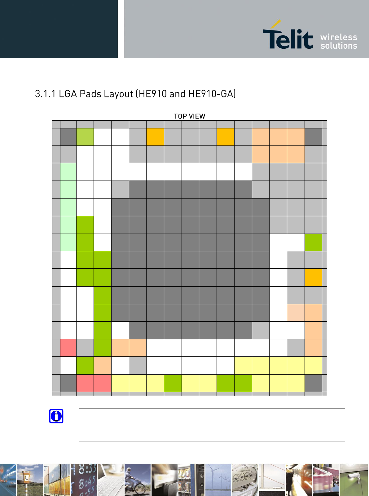
Reproduction forbidden without Telit Communications S.p.A. written authorization - All Rights Reserved page 18 of 91
A
B
C
D
E
F
G
H
J
K
L
M
N
P
R
1
ADC_IN1
RES
RES
GND
ANT_DIV
GND
GND
GND
ANT
GND
VBATT
VBATT_
PA
VBATT_
PA
2
GND
RES
RES
RES
GND
GND
GND
GND
GND
GND
GND
VBATT
VBATT_
PA
VBATT_
PA
GND
3
SIMVC
C
RES
RES
RES
RES
RES
RES
RES
RES
RES
RES
GND
GND
GND
GND
4
SIMIN
RES
RES
GND
GND
GND
GND
GND
5
SIMIO
RES
RES
GND
GND
GND
6
SIMCLK
DVI_RX
RES
GND
GND
GND
7
SIMRS
T
DVI_TX
RES
RES
RES
GPS_LN
A_EN
8
RES
DVI_CLK
GPIO_01
RES
GND
GND
9
RES
DVI_WA
0
GPIO_02
RES
GND
ANT_GP
S
10
RES
RES
GPIO_03
RES
GND
GND
11
RES
RES
GPIO_04
RES
RESET*
VAUX/P
WRMON
12
RES
RES
GPIO_06
RES
GND
RES
RES
ON_OFF
*
13
VUSB
GND
GPIO_07
VDD_IO
1
1V8_SEL
RES
RES
RES
RES
RES
RES
RES
RES
GND
HW_SH
UTDOW
N*
14
RES
GPIO_05
VRTC
RES
GND
RES
RES
RES
RES
RES
C105/RT
S
C108/DT
R
C109/DC
D
C107/DS
R
C125/RI
NG
15
USB_D+
USB_D-
TX AUX
RX AUX
SPI_CLK
GPIO_10
SPI_MR
DY
SPI_SR
DY
GPIO_08
GPIO_09
C104/RX
D
C103/TX
D
C106/CT
S
NOTE:
The pin defined as RES has to be considered RESERVED and not connected on any pin in the
application.
HE910 Hardware User Guide
1vv0300925 Rev.18 – 15-06-2012
Reproduction forbidden without Telit Communications S.p.A. written authorization - All Rights Reserved page 19 of 91
A
B
C
D
E
F
G
H
J
K
L
M
N
P
R
1
ADC_IN1
RES
RES
GND
ANT_DIV
GND
GND
GND
ANT
GND
VBATT
VBATT_
PA
VBATT_
PA
2
GND
RES
RES
RES
GND
GND
GND
GND
GND
GND
GND
VBATT
VBATT_
PA
VBATT_
PA
GND
3
SIMVC
C
RES
RES
RES
RES
RES
RES
RES
RES
RES
RES
GND
GND
GND
GND
4
SIMIN
RES
RES
GND
GND
GND
GND
GND
5
SIMIO
RES
RES
GND
GND
GND
6
SIMCLK
DVI_RX
RES
GND
GND
GND
7
SIMRS
T
DVI_TX
RES
RES
RES
RES
8
RES
DVI_CLK
GPIO_01
RES
GND
GND
9
RES
DVI_WA
0
GPIO_02
RES
GND
RES
10
RES
RES
GPIO_03
RES
GND
GND
11
RES
RES
GPIO_04
RES
RESET*
VAUX/P
WRMON
12
RES
RES
GPIO_06
RES
GND
RES
RES
ON_OFF
*
13
VUSB
GND
GPIO_07
VDD_IO
1
1V8_SEL
RES
RES
RES
RES
RES
RES
RES
RES
GND
HW_SH
UTDOW
N*
14
RES
GPIO_05
VRTC
RES
GND
RES
RES
RES
RES
RES
C105/RT
S
C108/DT
R
C109/DC
D
C107/DS
R
C125/RI
NG
15
USB_D+
USB_D-
TX AUX
RX AUX
SPI_CLK
GPIO_10
SPI_MR
DY
SPI_SR
DY
GPIO_08
GPIO_09
C104/RX
D
C103/TX
D
C106/CT
S
NOTE:
The pin defined as RES has to be considered RESERVED and not connected on any pin in the
application.
HE910 Hardware User Guide
1vv0300925 Rev.18 – 15-06-2012
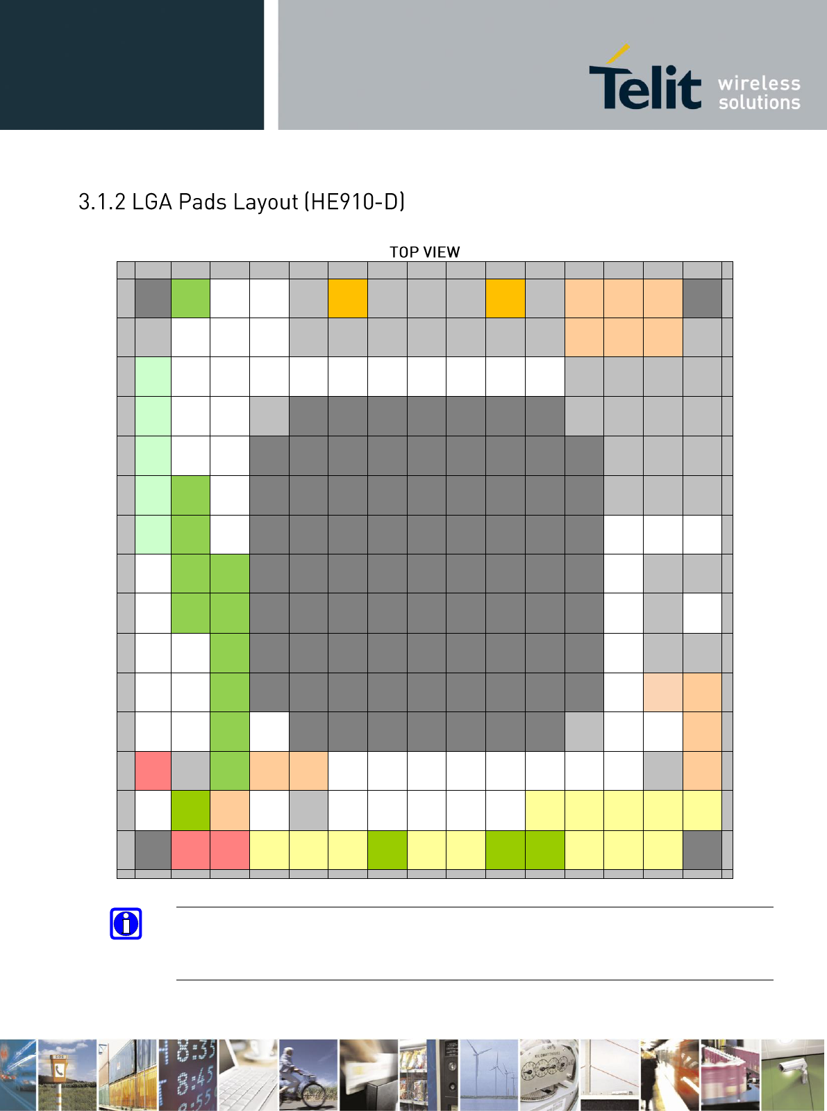
Reproduction forbidden without Telit Communications S.p.A. written authorization - All Rights Reserved page 20 of 91
A
B
C
D
E
F
G
H
J
K
L
M
N
P
R
1
ADC_IN1
RES
RES
GND
RES
GND
GND
GND
ANT
GND
VBATT
VBATT_
PA
VBATT_
PA
2
GND
RES
RES
RES
GND
GND
GND
GND
GND
GND
GND
VBATT
VBATT_
PA
VBATT_
PA
GND
3
SIMVC
C
RES
RES
RES
RES
RES
RES
RES
RES
RES
RES
GND
GND
GND
GND
4
SIMIN
RES
RES
GND
GND
GND
GND
GND
5
SIMIO
RES
RES
GND
GND
GND
6
SIMCLK
DVI_RX
RES
GND
GND
GND
7
SIMRS
T
DVI_TX
RES
RES
RES
RES
8
RES
DVI_CLK
GPIO_01
RES
GND
GND
9
RES
DVI_WA
0
GPIO_02
RES
GND
RES
10
RES
RES
GPIO_03
RES
GND
GND
11
RES
RES
GPIO_04
RES
RESET*
VAUX/P
WRMON
12
RES
RES
GPIO_06
RES
GND
RES
RES
ON_OFF
*
13
VUSB
GND
GPIO_07
VDD_IO
1
1V8_SEL
RES
RES
RES
RES
RES
RES
RES
RES
GND
HW_SH
UTDOW
N*
14
RES
GPIO_05
VRTC
RES
GND
RES
RES
RES
RES
RES
C105/RT
S
C108/DT
R
C109/DC
D
C107/DS
R
C125/RI
NG
15
USB_D+
USB_D-
TX AUX
RX AUX
SPI_CLK
GPIO_10
SPI_MR
DY
SPI_SR
DY
GPIO_08
GPIO_09
C104/RX
D
C103/TX
D
C106/CT
S
NOTE:
The pin defined as RES has to be considered RESERVED and not connected on any pin in the
application.
HE910 Hardware User Guide
1vv0300925 Rev.18 – 15-06-2012
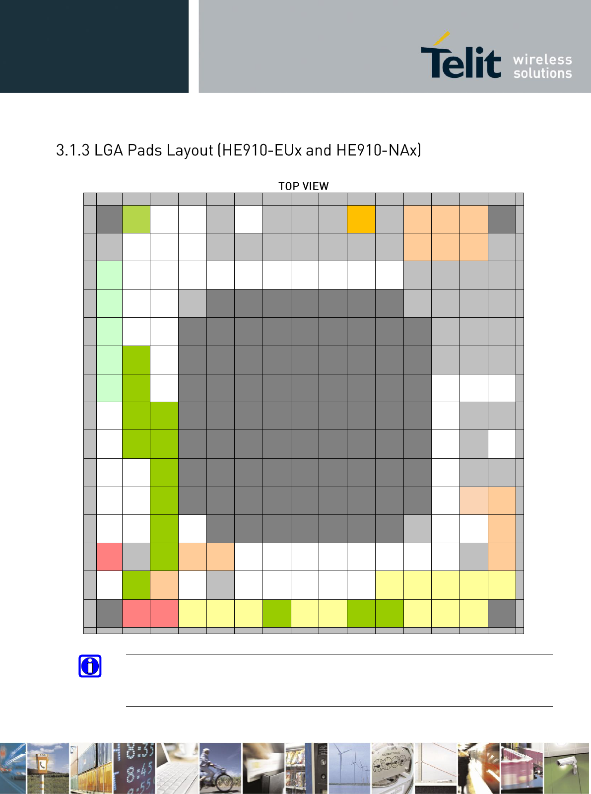
Reproduction forbidden without Telit Communications S.p.A. written authorization - All Rights Reserved page 21 of 91
A
B
C
D
E
F
G
H
J
K
L
M
N
P
R
1
ADC_IN1
RES
RES
GND
RES
GND
GND
GND
ANT
GND
VBATT
VBATT_
PA
VBATT_
PA
2
GND
RES
RES
RES
GND
GND
GND
GND
GND
GND
GND
VBATT
VBATT_
PA
VBATT_
PA
GND
3
SIMVC
C
RES
RES
RES
RES
RES
RES
RES
RES
RES
RES
GND
GND
GND
GND
4
SIMIN
RES
RES
GND
GND
GND
GND
GND
5
SIMIO
RES
RES
GND
GND
GND
6
SIMCLK
DVI_RX
RES
GND
GND
GND
7
SIMRS
T
DVI_TX
RES
RES
RES
GPS_LN
A_EN
8
RES
DVI_CLK
GPIO_01
RES
GND
GND
9
RES
DVI_WA
0
GPIO_02
RES
GND
ANT_GP
S
10
RES
RES
GPIO_03
RES
GND
GND
11
RES
RES
GPIO_04
RES
RESET*
VAUX/P
WRMON
12
RES
RES
GPIO_06
RES
GND
RES
RES
ON_OFF
*
13
VUSB
GND
GPIO_07
VDD_IO
1
1V8_SEL
RES
RES
RES
RES
RES
RES
RES
RES
GND
HW_SH
UTDOW
N*
14
RES
GPIO_05
VRTC
RES
GND
RES
RES
RES
RES
RES
C105/RT
S
C108/DT
R
C109/DC
D
C107/DS
R
C125/RI
NG
15
USB_D+
USB_D-
TX AUX
RX AUX
SPI_CLK
GPIO_10
SPI_MR
DY
SPI_SR
DY
GPIO_08
GPIO_09
C104/RX
D
C103/TX
D
C106/CT
S
NOTE:
The pin defined as RES has to be considered RESERVED and not connected on any pin in the
application.
HE910 Hardware User Guide
1vv0300925 Rev.18 – 15-06-2012
Reproduction forbidden without Telit Communications S.p.A. written authorization - All Rights Reserved page 22 of 91
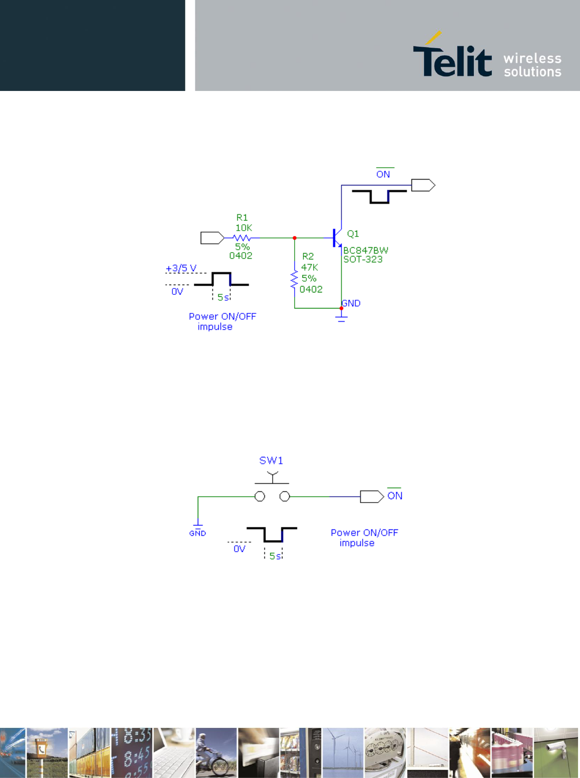
To turn on the HE910 the pad ON_OFF* must be tied low for at least 5 seconds and then
released.
The maximum current that can be drained from the ON# pad is 0,1 mA.
A simple circuit to do it is:
NOTE:
Don't use any pull up resistor on the ON_OFF* line, it is internally pulled up. Using pull up
resistor may bring to latch up problems on the HE910 power regulator and improper power
on/off of the module. The line ON_OFF* must be connected only in open collector or open
drain configuration.
HE910 Hardware User Guide
1vv0300925 Rev.18 – 15-06-2012
Reproduction forbidden without Telit Communications S.p.A. written authorization - All Rights Reserved page 23 of 91
NOTE:
In this document all the lines that are inverted, hence have active low signals are labelled with a
name that ends with”#",”*” or with a bar over the name.
TIP:
To check if the device has powered on, the hardware line PWRMON should be monitored.
NOTE:
It is mandatory to avoid sending data to the serial ports during the first 200ms of the module
start-up.
HE910 Hardware User Guide
1vv0300925 Rev.18 – 15-06-2012
Reproduction forbidden without Telit Communications S.p.A. written authorization - All Rights Reserved page 24 of 91
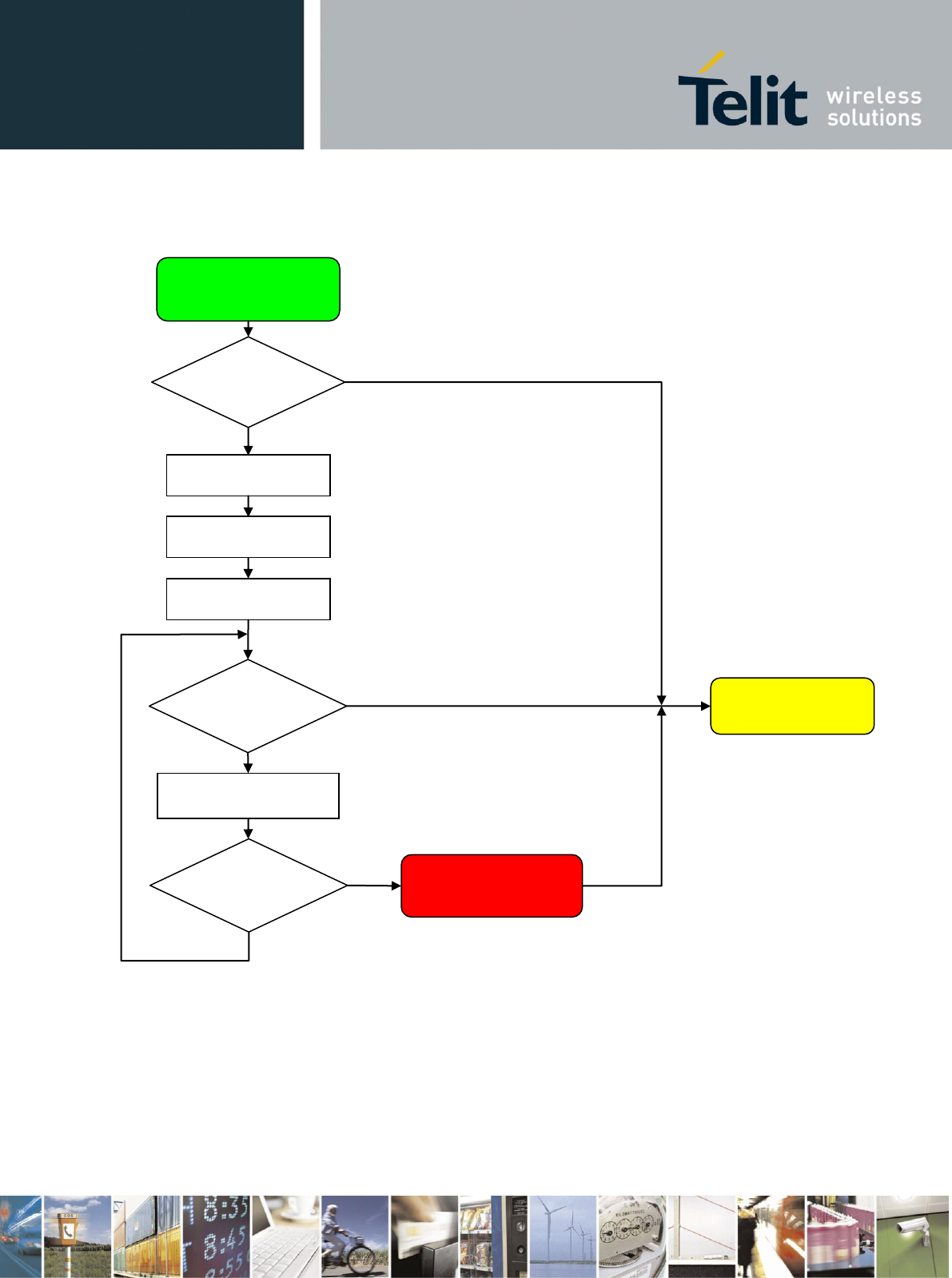
A flow chart showing the proper turn on procedure is displayed below:
NOTE:
In order to avoid a back powering effect it is recommended to avoid having any HIGH logic
level signal applied to the digital pins of the HE910 when the module is powered off or during
an ON/OFF transition.
Modem ON Proc.
Y
Y
HW unconditional
SHUTDOWN
AT init sequence.
Start AT CMD.
N
PWMON = ON?
PWMON = ON?
AT answer in 1Sec ?
N
Y
N
Delay 1s
DELAY= 300mSec
ON_OFF = LOW
Delay = 5 Sec
ON_OFF = HIGH
Enter AT<CR>
HE910 Hardware User Guide
1vv0300925 Rev.18 – 15-06-2012
Reproduction forbidden without Telit Communications S.p.A. written authorization - All Rights Reserved page 25 of 91
A flow chart showing the AT command managing procedure is displayed below:
AT answer in
1Sec ?
Y
N
Start AT CMD.
DELAY= 300mSec
Enter AT<CR>
AT init sequence.
Modem ON Proc.
HW unconditional
SHUTDOWN
HE910 Hardware User Guide
1vv0300925 Rev.18 – 15-06-2012
Reproduction forbidden without Telit Communications S.p.A. written authorization - All Rights Reserved page 26 of 91
For example:
1- Let's assume you need to drive the ON# pad with a totem pole output of a +3/5 V
microcontroller (uP_OUT1):
2- Let's assume you need to drive the ON# pad directly with an ON/OFF button:
HE910 Hardware User Guide
1vv0300925 Rev.18 – 15-06-2012
Reproduction forbidden without Telit Communications S.p.A. written authorization - All Rights Reserved page 27 of 91
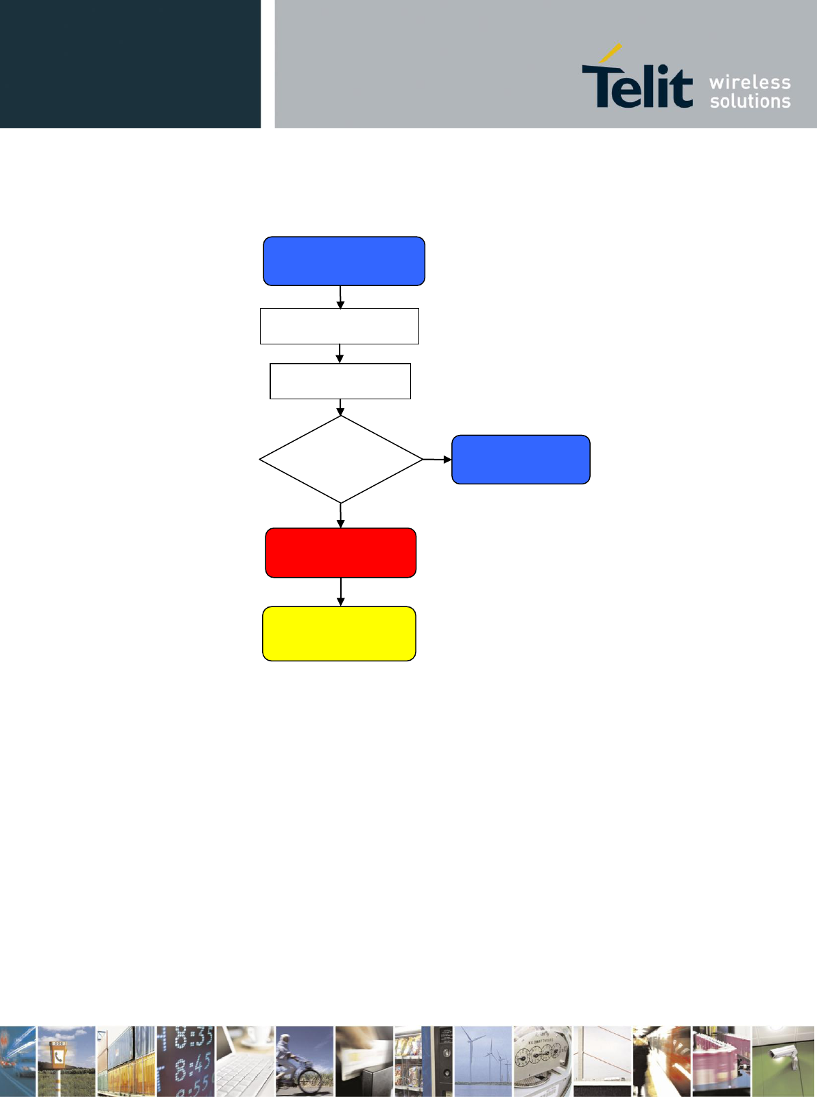
Turning off of the device can be done in two ways:
via AT command (see HE910 Software User Guide, AT#SHDN)
by tying low pin ON_OFF*
Either ways, the device issues a detach request to network informing that the device will not be
reachable any more.
To turn OFF the HE910 the pad ON_OFF* must be tied low for at least 2 seconds and then
released.
TIP:
To check if the device has been powered off, the hardware line PWRMON must be monitored.
The device is powered off when PWRMON goes low.
NOTE:
In order to avoid a back powering effect it is recommended to avoid having any HIGH logic
level signal applied to the digital pins of the HE910 when the module is powered off or during
an ON/OFF transition.
HE910 Hardware User Guide
1vv0300925 Rev.18 – 15-06-2012
Reproduction forbidden without Telit Communications S.p.A. written authorization - All Rights Reserved page 28 of 91
The following flow chart shows the proper turn off procedure:
Modem OFF Proc.
N
Y
HW unconditional
SHUTDOWN
N
PWMON = ON?
PWMON = ON?
Y
Delay 15s
ON_OFF = LOW
Delay = 2 Sec
ON_OFF = HIGH
Modem ON Proc.
PWMON = ON?
N
Y
HE910 Hardware User Guide
1vv0300925 Rev.18 – 15-06-2012
Reproduction forbidden without Telit Communications S.p.A. written authorization - All Rights Reserved page 29 of 91
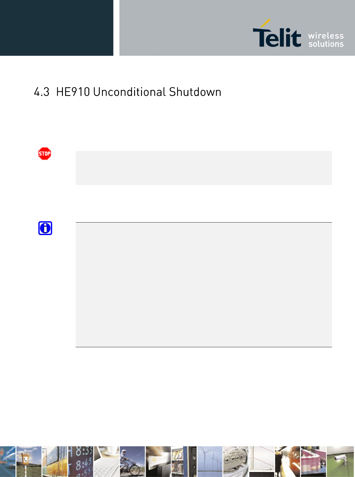
The Unconditional Shutdown of the module could be activated using the
HW_SHUTDOWN* line (pad R13).
WARNING:
The hardware unconditional Shutdown must not be used during normal operation of the device
since it does not detach the device from the network. It shall be kept as an emergency exit
procedure.
To unconditionally shutdown the HE910, the pad HW_SHUTDOWN* must be tied low for at
least 200 milliseconds and then released.
NOTE:
Do not use any pull up resistor on the HW_SHUTDOWN* line nor any totem pole digital
output. Using pull up resistor may bring to latch up problems on the HE910 power regulator and
improper functioning of the module. The line HW_SHUTDOWN* must be connected only in
open collector configuration.
The HW_SHUTDOWN* is generating an unconditional shutdown of the module without an
automatic restart.
The module will shutdown, but will NOT perform the detach from the cellular network.
To proper power on again the module please refer to the related paragraph (“Powering ON the
HE910”)
TIP:
The unconditional hardware shutdown must always be implemented on the boards and should be
used only as an emergency exit procedure.
HE910 Hardware User Guide
1vv0300925 Rev.18 – 15-06-2012
Reproduction forbidden without Telit Communications S.p.A. written authorization - All Rights Reserved page 30 of 91
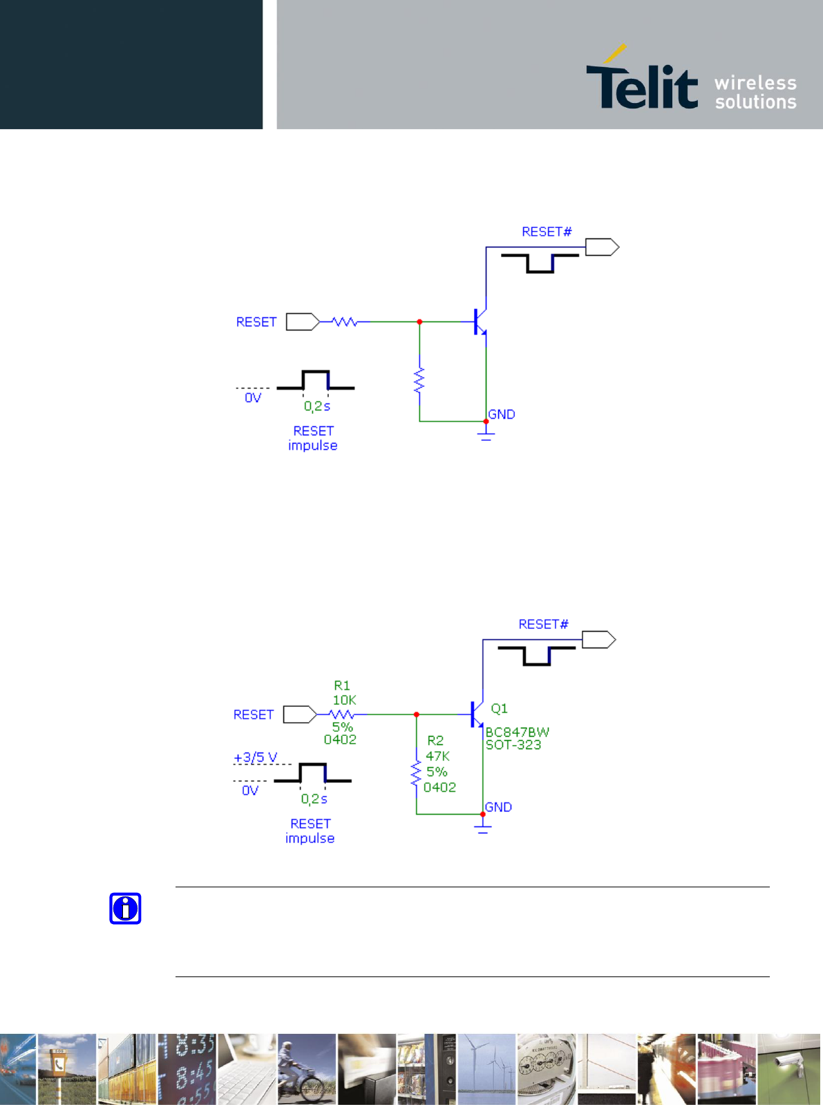
A typical circuit is the following:
For example:
1- Let us assume you need to drive the HW_SHUTDOWN* pad with a totem pole output of
a +3/5 V microcontroller (uP_OUT2):
NOTE:
In order to avoid a back powering effect it is recommended to avoid having any HIGH logic
level signal applied to the digital pins of the HE910 when the module is powered off or during
an ON/OFF transition.
HE910 Hardware User Guide
1vv0300925 Rev.18 – 15-06-2012
Reproduction forbidden without Telit Communications S.p.A. written authorization - All Rights Reserved page 31 of 91
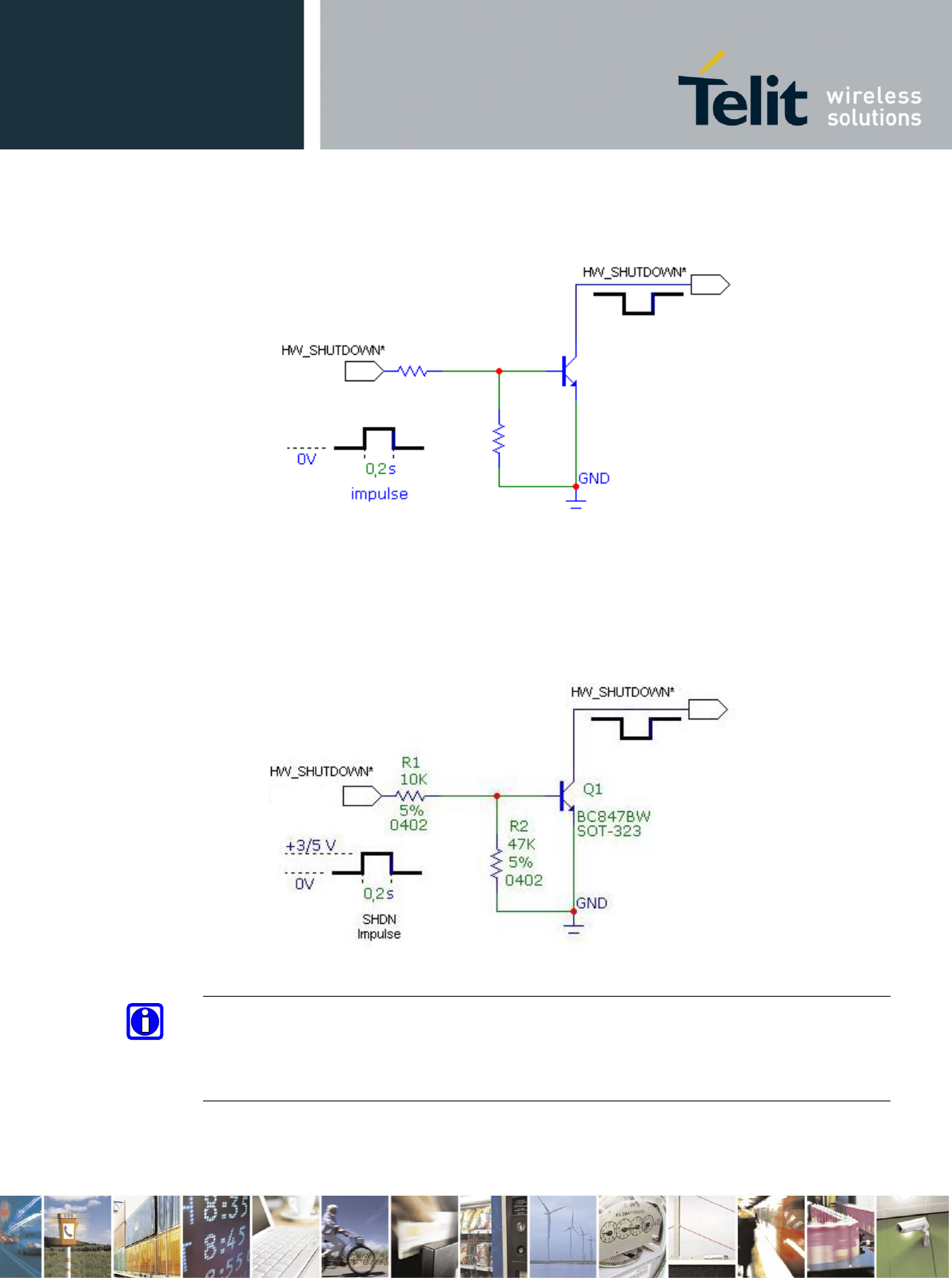
In the following flow chart is detailed the proper restart procedure:
HW unconditional
SHUTDOWN
HW_SHUTDOWN*=
LOW
= LOW
Delay 200ms
HW_SHUTDOWN*=
HIGH
PWRMON = ON
Delay 1s
Modem ON Proc.
N
Y
Disconnect PWR
supply
Modem ON Proc.
HE910 Hardware User Guide
1vv0300925 Rev.18 – 15-06-2012
Reproduction forbidden without Telit Communications S.p.A. written authorization - All Rights Reserved page 32 of 91
The Unconditional Restart of the module could be activated using the
RESET* line (pad P11).
WARNING:
The hardware unconditional Restart must not be used during normal operation of the device
since it does not detach the device from the network. It shall be kept as an emergency exit
procedure.
To unconditionally Restart the HE910, the pad RESET* must be tied low for at
least 200 milliseconds and then released.
NOTE:
Do not use any pull up resistor on the RESET* line nor any totem pole digital output. Using pull
up resistor may bring to latch up problems on the HE910 power regulator and improper
functioning of the module. The line RESET* must be connected only in open collector
configuration.
The module will Restart and will NOT perform the detach from the cellular network.
TIP:
The unconditional hardware Restart should be implemented on the boards and should be used
only as an emergency exit procedure.
HE910 Hardware User Guide
1vv0300925 Rev.18 – 15-06-2012
Reproduction forbidden without Telit Communications S.p.A. written authorization - All Rights Reserved page 33 of 91
A typical circuit is the following:
For example:
1- Let us assume you need to drive the RESET* pad with a totem pole output of a +3/5 V
microcontroller (uP_OUT2):
NOTE:
In order to avoid a back powering effect it is recommended to avoid having any HIGH logic
level signal applied to the digital pins of the HE910 when the module is powered off or during
an ON/OFF transition.
HE910 Hardware User Guide
1vv0300925 Rev.18 – 15-06-2012
Reproduction forbidden without Telit Communications S.p.A. written authorization - All Rights Reserved page 34 of 91
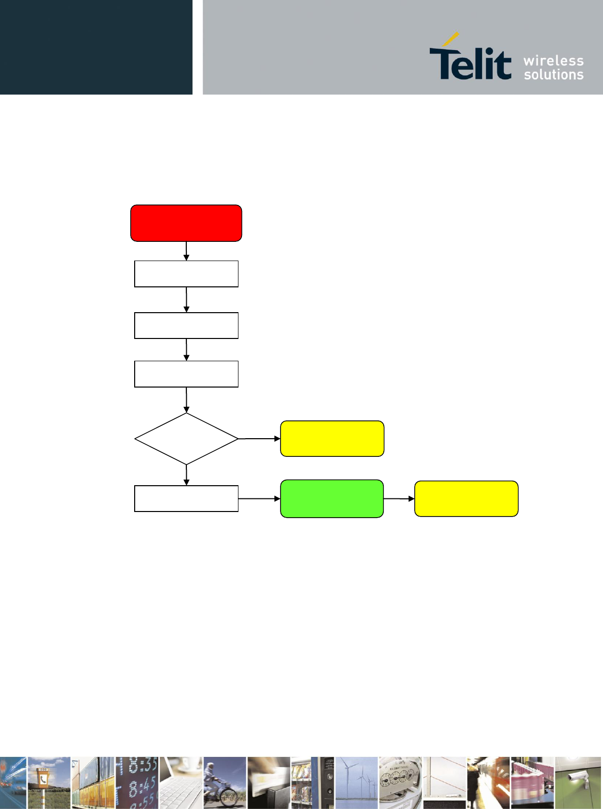
In the following flow chart is detailed the proper restart procedure:
HW unconditional
Restart
Reset* = LOW
Delay 200ms
Reset* = HIGH
PWRMON = ON
Delay 1s
Modem Startup
N
Y
Disconnect PWR
supply
Modem ON Proc.
HE910 Hardware User Guide
1vv0300925 Rev.18 – 15-06-2012
Reproduction forbidden without Telit Communications S.p.A. written authorization - All Rights Reserved page 35 of 91
The power supply circuitry and board layout are a very important part in the full product design
and they strongly reflect on the product overall performances, hence read carefully the
requirements and the guidelines that will follow for a proper design.
The external power supply must be connected to VBATT & VBATT_PA signals and must fulfil
the following requirements:
POWER SUPPLY
Nominal Supply Voltage
3.8 V
Normal Operating Voltage Range
3.40 V÷ 4.20 V
Extended Operating Voltage Range
3.10 V÷ 4.50 V
NOTE:
The Operating Voltage Range MUST never be exceeded; care must be taken when designing the
application’s power supply section to avoid having an excessive voltage drop.
If the voltage drop is exceeding the limits it could cause a Power Off of the module.
NOTE:
Overshoot voltage (regarding MAX Extended Operating Voltage) and drop in voltage
(regarding MIN Extended Operating Voltage) MUST never be exceeded;
The “Extended Operating Voltage Range” can be used only with completely assumption and
application of the HW User guide suggestions.
HE910 Hardware User Guide
1vv0300925 Rev.18 – 15-06-2012
Reproduction forbidden without Telit Communications S.p.A. written authorization - All Rights Reserved page 36 of 91
HE910
Mode
Average
(mA)
Mode description
SWITCHED OFF
Module supplied but Switched Off
Switched Off
40uA
IDLE mode (WCDMA)
AT+CFUN=5
1.2
Disabled TX and RX; DRX7
IDLE mode (GSM/EDGE)
AT+CFUN=1
19
Normal mode: full functionality of the module
AT+CFUN=4
16.5
Disabled TX and RX; module is not registered on the network
AT+CFUN=5
0.8
Disabled TX and RX; DRX9 (1.1mA in case of DRX5)
Operative mode (WCDMA)
WCDMA Voice
152
WCDMA voice call (TX = 10dBm)
WCDMA HSDPA (0dBm)
187
WCDMA data call (Cat 14, TX = 0dBm)
WCDMA HSDPA (22dBm)
494
WCDMA data call (Cat 14, TX = 22dBm)
Operative mode (EDGE)
EDGE 4TX+2RX
EDGE Sending data mode
GSM900 PL5
495
DCS1800 PL0
484
Operative mode (GSM)
CSD TX and RX mode
GSM VOICE CALL
GSM900 CSD PL5
220
DCS1800 CSD PL0
167
GPRS 4TX+2RX
GPRS Sending data mode
GSM900 PL5
580
DCS1800 PL0
438
The GSM system is made in a way that the RF transmission is not continuous, else it is packed
into bursts at a base frequency of about 216 Hz, and the relative current peaks can be as high as
about 2A. Therefore the power supply has to be designed in order to withstand with these
current peaks without big voltage drops; this means that both the electrical design and the board
layout must be designed for this current flow. If the layout of the PCB is not well designed a
strong noise floor is generated on the ground and the supply; this will reflect on all the audio
paths producing an audible annoying noise at 216 Hz; if the voltage drop during the peak current
absorption is too much, then the device may even shutdown as a consequence of the supply
voltage drop.
NOTE:
The electrical design for the Power supply should be made ensuring it will be capable of a peak
current output of at least 2 A.

HE910 Hardware User Guide
1vv0300925 Rev.18 – 15-06-2012
Reproduction forbidden without Telit Communications S.p.A. written authorization - All Rights Reserved page 37 of 91
The principal guidelines for the Power Supply Design embrace three different design steps:
the electrical design
the thermal design
the PCB layout.
The electrical design of the power supply depends strongly from the power source where this
power is drained. We will distinguish them into three categories:
+5V input (typically PC internal regulator output)
+12V input (typically automotive)
Battery
The desired output for the power supply is 3.8V, hence there's not a big difference between
the input source and the desired output and a linear regulator can be used. A switching
power supply will not be suited because of the low drop out requirements.
When using a linear regulator, a proper heat sink shall be provided in order to dissipate the
power generated.
A Bypass low ESR capacitor of adequate capacity must be provided in order to cut the
current absorption peaks close to the HE910, a 100μF tantalum capacitor is usually suited.
Make sure the low ESR capacitor on the power supply output (usually a tantalum one) is
rated at least 10V.
A protection diode should be inserted close to the power input, in order to save the HE910
from power polarity inversion.
HE910 Hardware User Guide
1vv0300925 Rev.18 – 15-06-2012
Reproduction forbidden without Telit Communications S.p.A. written authorization - All Rights Reserved page 38 of 91
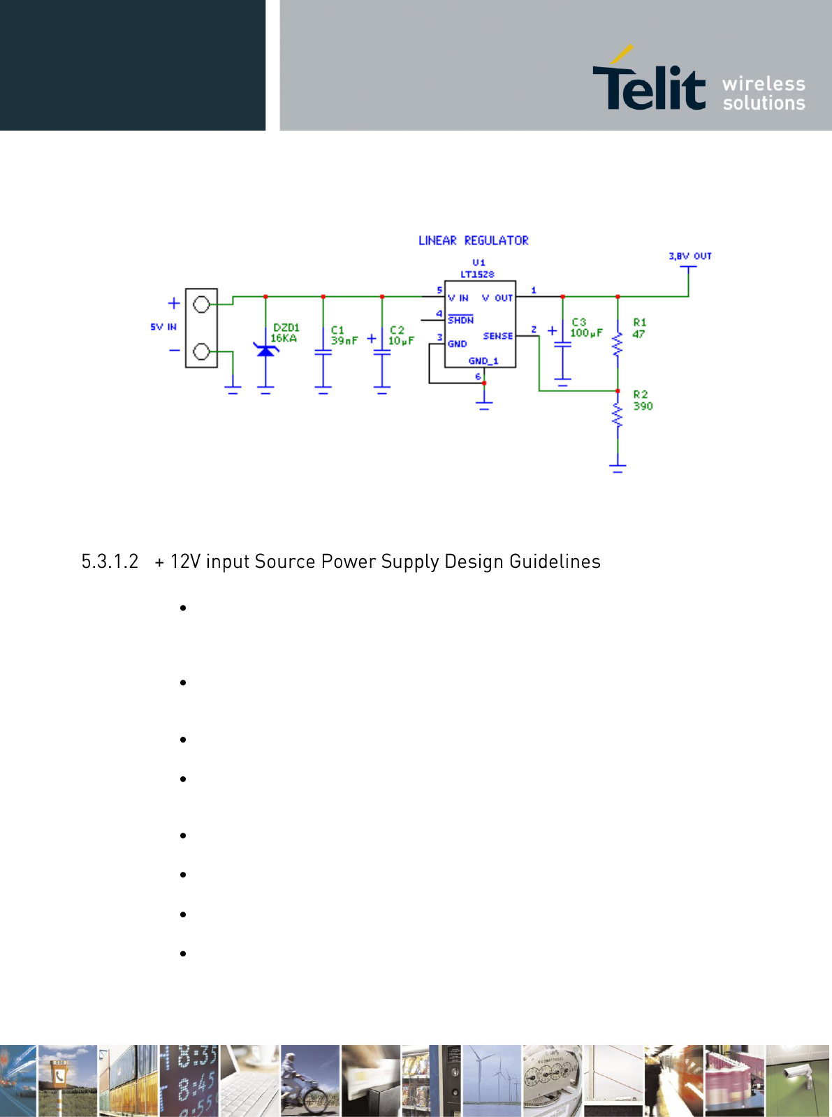
An example of linear regulator with 5V input is:
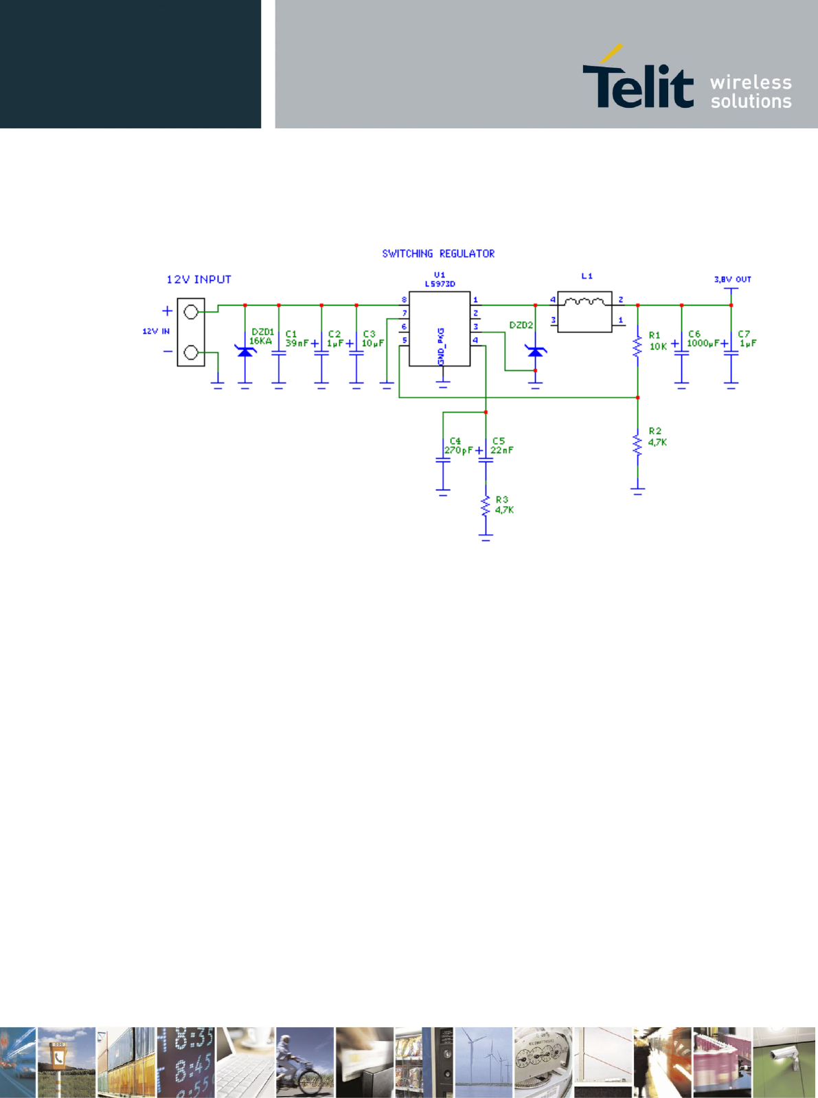
The desired output for the power supply is 3.8V, hence due to the big difference between the
input source and the desired output, a linear regulator is not suited and shall not be used. A
switching power supply will be preferable because of its better efficiency especially with the
2A peak current load represented by the HE910.
When using a switching regulator, a 500kHz or more switching frequency regulator is
preferable because of its smaller inductor size and its faster transient response. This allows
the regulator to respond quickly to the current peaks absorption.
In any case the frequency and Switching design selection is related to the application to be
developed due to the fact the switching frequency could also generate EMC interferences.
For car PB battery the input voltage can rise up to 15,8V and this should be kept in mind
when choosing components: all components in the power supply must withstand this
voltage.
A Bypass low ESR capacitor of adequate capacity must be provided in order to cut the
current absorption peaks, a 100μF tantalum capacitor is usually suited.
Make sure the low ESR capacitor on the power supply output (usually a tantalum one) is
rated at least 10V.
For Car applications a spike protection diode should be inserted close to the power input, in
order to clean the supply from spikes.
A protection diode should be inserted close to the power input, in order to save the HE910
from power polarity inversion. This can be the same diode as for spike protection.
HE910 Hardware User Guide
1vv0300925 Rev.18 – 15-06-2012
Reproduction forbidden without Telit Communications S.p.A. written authorization - All Rights Reserved page 39 of 91
An example of switching regulator with 12V input is in the below schematic:
HE910 Hardware User Guide
1vv0300925 Rev.18 – 15-06-2012
Reproduction forbidden without Telit Communications S.p.A. written authorization - All Rights Reserved page 40 of 91
The desired nominal output for the power supply is 3.8V and the maximum voltage
allowed is 4.2V, hence a single 3.7V Li-Ion cell battery type is suited for supplying the
power to the Telit HE910 module.
WARNING:
The three cells Ni/Cd or Ni/MH 3,6 V Nom. battery types or 4V PB types MUST NOT BE
USED DIRECTLY since their maximum voltage can rise over the absolute maximum voltage
for the HE910 and damage it.
NOTE:
DON'T USE any Ni-Cd, Ni-MH, and Pb battery types directly connected with HE910. Their use
can lead to overvoltage on the HE910 and damage it. USE ONLY Li-Ion battery types.
A Bypass low ESR capacitor of adequate capacity must be provided in order to cut the current
absorption peaks, a 100μF tantalum capacitor is usually suited.
Make sure the low ESR capacitor (usually a tantalum one) is rated at least 10V.
A protection diode should be inserted close to the power input, in order to save the HE910 from
power polarity inversion. Otherwise the battery connector should be done in a way to avoid
polarity inversions when connecting the battery.
The battery capacity must be at least 500mAh in order to withstand the current peaks of 2A; the
suggested capacity is from 500mAh to 1000mAh.
HE910 Hardware User Guide
1vv0300925 Rev.18 – 15-06-2012
Reproduction forbidden without Telit Communications S.p.A. written authorization - All Rights Reserved page 41 of 91
The thermal design for the power supply heat sink should be done with the following
specifications:
Average current consumption during HSDPA transmission @PWR level max :
600 mA
Average current during idle:
1.5 mA
NOTE:
The average consumption during transmissions depends on the power level at which the device
is requested to transmit by the network. The average current consumption hence varies
significantly.
Considering the very low current during idle, especially if Power Saving function is enabled, it
is possible to consider from the thermal point of view that the device absorbs current
significantly only during calls.
If we assume that the device stays into transmission for short periods of time (let's say few
minutes) and then remains for a quite long time in idle (let's say one hour), then the power
supply has always the time to cool down between the calls and the heat sink could be smaller
than the calculated one for 600mA maximum RMS current, or even could be the simple chip
package (no heat sink).
Moreover in the average network conditions the device is requested to transmit at a lower power
level than the maximum and hence the current consumption will be less than the 600mA, being
usually around 150mA.
For these reasons the thermal design is rarely a concern and the simple ground plane where the
power supply chip is placed can be enough to ensure a good thermal condition and avoid
overheating.
For the heat generated by the HE910, you can consider it to be during transmission 1W max
during CSD/VOICE calls and 2W max during class10 GPRS upload.
This generated heat will be mostly conducted to the ground plane under the HE910; you must
ensure that your application can dissipate it.

HE910 Hardware User Guide
1vv0300925 Rev.18 – 15-06-2012
Reproduction forbidden without Telit Communications S.p.A. written authorization - All Rights Reserved page 42 of 91
As seen on the electrical design guidelines the power supply shall have a low ESR capacitor on
the output to cut the current peaks and a protection diode on the input to protect the supply from
spikes and polarity inversion. The placement of these components is crucial for the correct
working of the circuitry. A misplaced component can be useless or can even decrease the power
supply performances.
The Bypass low ESR capacitor must be placed close to the Telit HE910 power
input pads or in the case the power supply is a switching type it can be placed close
to the inductor to cut the ripple provided the PCB trace from the capacitor to the
HE910 is wide enough to ensure a dropless connection even during the 2A current
peaks.
The protection diode must be placed close to the input connector where the power
source is drained.
The PCB traces from the input connector to the power regulator IC must be wide
enough to ensure no voltage drops occur when the 2A current peaks are absorbed.
Note that this is not made in order to save power loss but especially to avoid the
voltage drops on the power line at the current peaks frequency of 216 Hz that will
reflect on all the components connected to that supply, introducing the noise floor at
the burst base frequency. For this reason while a voltage drop of 300-400 mV may
be acceptable from the power loss point of view, the same voltage drop may not be
acceptable from the noise point of view. If your application doesn't have audio
interface but only uses the data feature of the Telit HE910, then this noise is not so
disturbing and power supply layout design can be more forgiving.
The PCB traces to the HE910 and the Bypass capacitor must be wide enough to
ensure no significant voltage drops occur when the 2A current peaks are absorbed.
This is for the same reason as previous point. Try to keep this trace as short as
possible.
The PCB traces connecting the Switching output to the inductor and the switching
diode must be kept as short as possible by placing the inductor and the diode very
close to the power switching IC (only for switching power supply). This is done in
order to reduce the radiated field (noise) at the switching frequency (100-500 kHz
usually).
The use of a good common ground plane is suggested.
The placement of the power supply on the board should be done in such a way to
guarantee that the high current return paths in the ground plane are not overlapped
to any noise sensitive circuitry as the microphone amplifier/buffer or earphone
amplifier.
The power supply input cables should be kept separate from noise sensitive lines
such as microphone/earphone cables.
HE910 Hardware User Guide
1vv0300925 Rev.18 – 15-06-2012
Reproduction forbidden without Telit Communications S.p.A. written authorization - All Rights Reserved page 43 of 91
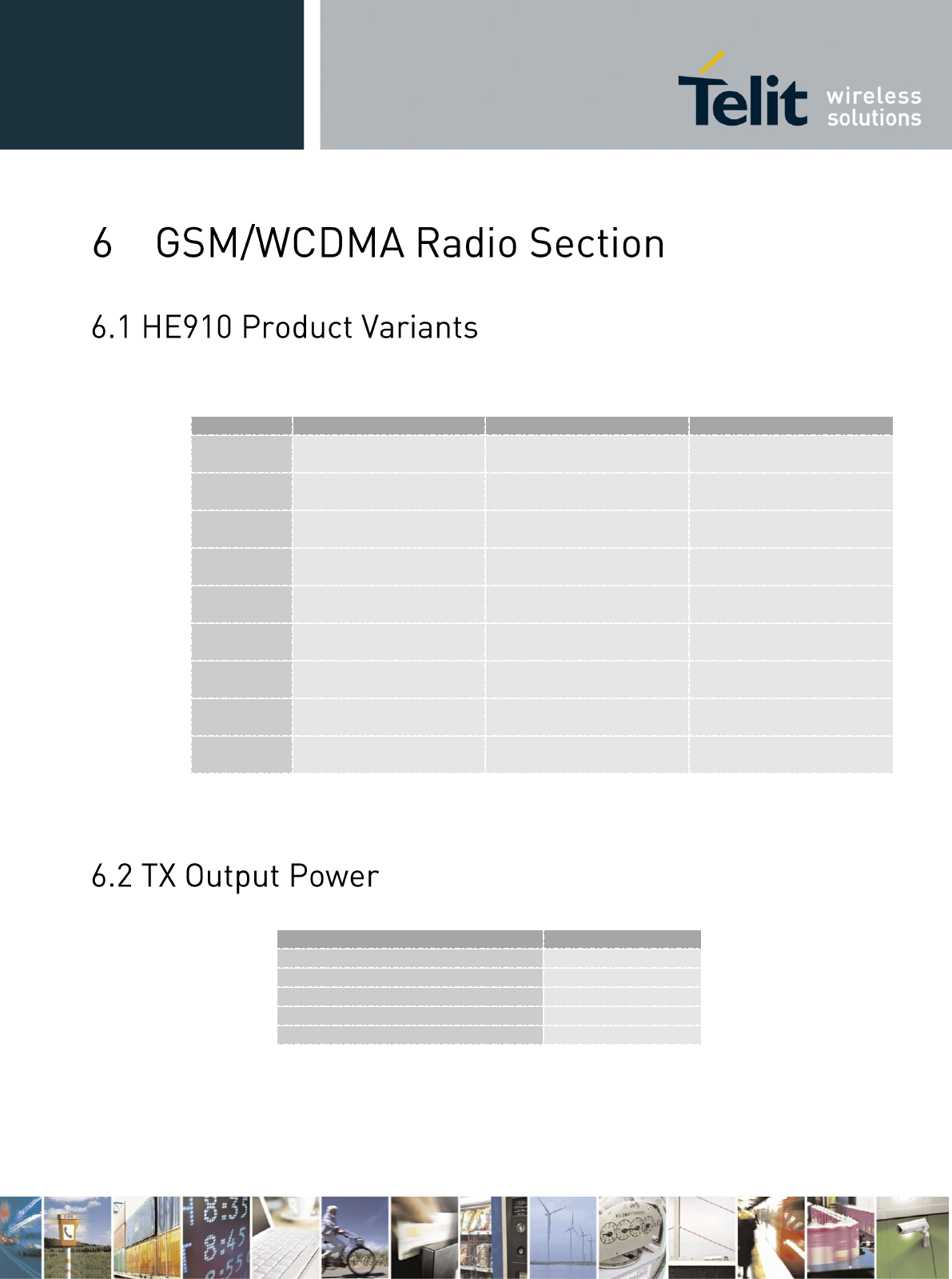
The following table is listing the main differences between the HE910 variants:
Product
Supported 2G Bands
Supported 3G bands
Antenna Diversity
HE910
GSM 850, GSM 900,
DCS1800, PCS 1900
FDD B1, B2, B4, B5, B8
FDD B1, B2, B5, B8 GSM
850, GSM 900, PCS 1900
HE910-D
GSM 850, GSM 900,
DCS1800, PCS 1900
FDD B1, B2, B4, B5, B8
FDD B1, B2, B5, B8 GSM
850, GSM 900, PCS 1900
HE910-GA
GSM 850, GSM 900,
DCS1800, PCS 1900
FDD B1, B2, B5, B8
FDD B1, B2, B5, B8 GSM
850, GSM 900, PCS 1900
HE910-EUR
GSM 850, GSM 900,
DCS1800, PCS 1900
FDD B1, B5, B8
NO
HE910-EUD
GSM 850, GSM 900,
DCS1800, PCS 1900
FDD B1, B5, B8
NO
HE910-EUG
GSM 850, GSM 900,
DCS1800, PCS 1900
FDD B1, B5, B8
NO
HE910-NAR
GSM 850, GSM 900,
DCS1800, PCS 1900
FDD B2, B4, B5
NO
HE910-NAD
GSM 850, GSM 900,
DCS1800, PCS 1900
FDD B2, B4, B5
NO
HE910-NAG
GSM 850, GSM 900,
DCS1800, PCS 1900
FDD B2, B4, B5
NO
Band
Power Class
GSM 850 / 900
4 (2W)
DCS1800 / PCS 1900
1 (1W)
EDGE, 850/900 MHz
E2 (0.5W)
EDGE, 1800/1900 MHz
Class E2 (0.4W)
WCDMA FDD B1, B2, B4, B5, B8
Class 3 (0.25W)
HE910 Hardware User Guide
1vv0300925 Rev.18 – 15-06-2012
Reproduction forbidden without Telit Communications S.p.A. written authorization - All Rights Reserved page 44 of 91
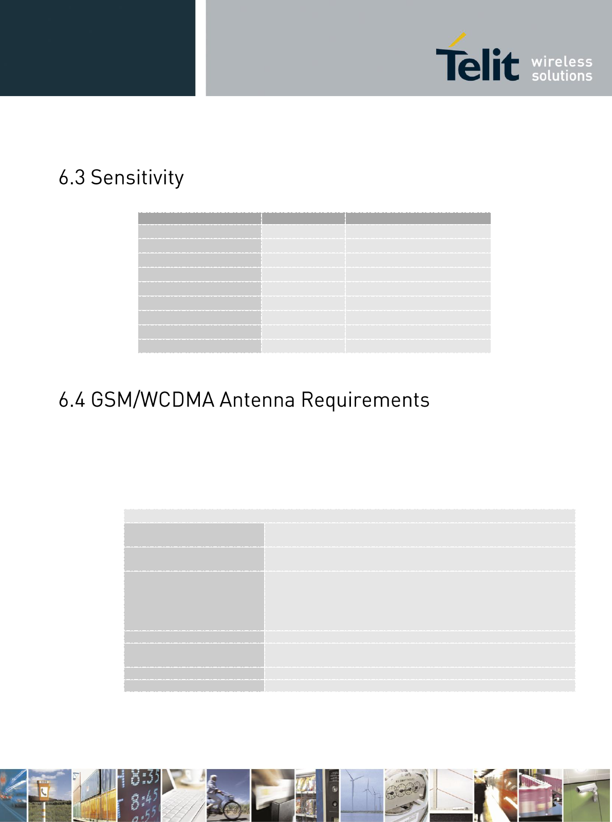
The antenna connection and board layout design are the most important aspect in the full
product design as they strongly affect the product overall performances, hence read carefully
and follow the requirements and the guidelines for a proper design.
The antenna and antenna transmission line on PCB for a Telit HE910 device shall fulfil the
following requirements:
ANTENNA REQUIREMENTS
Frequency range
Depending by frequency band(s) provided by the network operator, the
customer shall use the most suitable antenna for that/those band(s)
Bandwidth (GSM/EDGE)
70 MHz in GSM850, 80 MHz in GSM900, 170 MHz in DCS & 140
MHz PCS band
Bandwidth
(WCDMA)
70 MHz in WCDMA Band V
80 MHz in WCDMA Band VIII
460 MHz in WCDMA Band IV
140 MHz in WCDMA Band II
250 MHz in WCDMA Band I
Impedance
50 ohm
Input power
> 33dBm(2 W) peak power in GSM
> 24dBm Average power in WCDMA
VSWR absolute max
≤ 5:1 (limit to avoid permanent damage)
VSWR recommended
≤ 2:1 (limit to fulfil all regulatory requirements)
When using the HE910, since there's no antenna connector on the module, the antenna must
be connected to the HE910 antenna pad (K1) by means of a transmission line implemented
on the PCB.
Band
Typical
Note
GSM 850
-109.5 dBm
BER Class II <2.44%
GSM 900
-109 dBm
BER Class II <2.44%
DCS1800
-110 dBm
BER Class II <2.44%
PCS 1900
-109.5 dBm
BER Class II <2.44%
WCDMA FDD B1
-111 dBm
BER <0.01%
WCDMA FDD B2
-110 dBm
BER <0.01%
WCDMA FDD B4
-111 dBm
BER <0.01%
WCDMA FDD B5
-111 dBm
BER <0.01%
WCDMA FDD B8
-110 dBm
BER <0.01%
HE910 Hardware User Guide
1vv0300925 Rev.18 – 15-06-2012
Reproduction forbidden without Telit Communications S.p.A. written authorization - All Rights Reserved page 45 of 91
In the case the antenna is not directly connected at the antenna pad of the HE910, then a PCB
line is needed in order to connect with it or with its connector.
This transmission line shall fulfil the following requirements:
ANTENNA LINE ON PCB REQUIREMENTS
Characteristic Impedance
50 ohm
Max Attenuation
0,3 dB
Coupling with other signals shall be avoided
Cold End (Ground Plane) of antenna shall be equipotential to
the HE910 ground pins
Furthermore if the device is developed for the US market and/or Canada market, it shall
comply with the FCC and/or IC approval requirements:
This device is to be used only for mobile and fixed application. In order to re-use the Telit
FCC/IC approvals the antenna(s) used for this transmitter must be installed to provide a
separation distance of at least 20 cm from all persons and must not be co-located or operating
in conjunction with any other antenna or transmitter. If antenna is installed with a separation
distance of less than 20 cm from all persons or is co-located or operating in conjunction with
any other antenna or transmitter then additional FCC/IC testing may be required. End-Users
must be provided with transmitter operation conditions for satisfying RF exposure
compliance.
Antennas used for this OEM module must not exceed the gains for mobile and fixed
operating configurations as described in “FCC/IC Regulatory notices” chapter.
Make sure that the transmission line’s characteristic impedance is 50ohm ;
Keep line on the PCB as short as possible, since the antenna line loss shall be less than
around 0,3 dB;
Line geometry should have uniform characteristics, constant cross section, avoid meanders
and abrupt curves;
Any kind of suitable geometry / structure (Microstrip, Stripline, Coplanar, Grounded
Coplanar Waveguide...) can be used for implementing the printed transmission line afferent
the antenna;
If a Ground plane is required in line geometry, that plane has to be continuous and
sufficiently extended, so the geometry can be as similar as possible to the related canonical
model;
Keep, if possible, at least one layer of the PCB used only for the Ground plane; If possible,
use this layer as reference Ground plane for the transmission line;
It is wise to surround (on both sides) the PCB transmission line with Ground, avoid having
other signal tracks facing directly the antenna line track.

HE910 Hardware User Guide
1vv0300925 Rev.18 – 15-06-2012
Reproduction forbidden without Telit Communications S.p.A. written authorization - All Rights Reserved page 46 of 91
Avoid crossing any un-shielded transmission line footprint with other signal tracks on
different layers;
The ground surrounding the antenna line on PCB has to be strictly connected to the main
Ground Plane by means of via holes (once per 2mm at least), placed close to the ground
edges facing line track;
Place EM noisy devices as far as possible from HE910 antenna line;
Keep the antenna line far away from the HE910 power supply lines;
If EM noisy devices are present on the PCB hosting the HE910, such as fast switching ICs,
take care of the shielding of the antenna line by burying it inside the layers of PCB and
surround it with Ground planes, or shield it with a metal frame cover.
If EM noisy devices are not present around the line, the use of geometries like Microstrip or
Grounded Coplanar Waveguide has to be preferred, since they typically ensure less
attenuation if compared to a Stripline having same length;
Install the antenna in a place covered by the GSM signal.
If the device antenna is located greater then 20cm from the human body and there are no co-
located transmitter then the Telit FCC/IC approvals can be re-used by the end product
If the device antenna is located less then 20cm from the human body or there are no co-
located transmitter then the additional FCC/IC testing may be required for the end product
(Telit FCC/IC approvals cannot be reused)
Antenna shall not be installed inside metal cases
Antenna shall be installed also according Antenna manufacturer instructions.
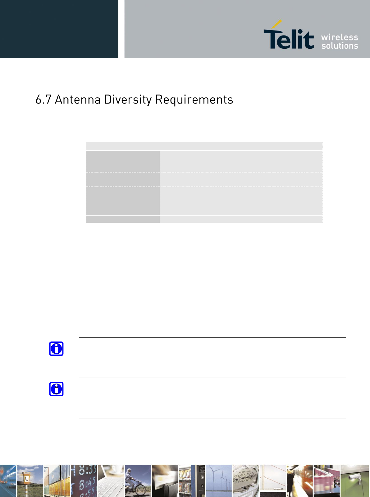
HE910 Hardware User Guide
1vv0300925 Rev.18 – 15-06-2012
Reproduction forbidden without Telit Communications S.p.A. written authorization - All Rights Reserved page 47 of 91
This product is including an input for a second RX antenna to improve the radio sensitivity. The
function is called Antenna Diversity.
ANTENNA REQUIREMENTS
Frequency range
Depending by frequency band(s) provided by the network
operator, the customer shall use the most suitable antenna for
that/those band(s)
Bandwidth (GSM/EDGE)
70 MHz in GSM850, 80 MHz in GSM900 & 140 MHz PCS
band
Bandwidth
(WCDMA)
70 MHz in WCDMA Band V
80 MHz in WCDMA Band VIII
140 MHz in WCDMA Band II
250 MHz in WCDMA Band I
Impedance
50 ohm
When using the HE910, since there's no antenna connector on the module, the antenna must be
connected to the HE910 antenna pad (F1) by means of a transmission line implemented on the
PCB.
In the case the antenna is not directly connected at the antenna pad of the HE910, then a PCB
line is needed in order to connect with it or with its connector.
The second Rx antenna should not be located in the close vicinity of main antenna. In order to
improve Diversity Gain, Isolation and reduce mutual interaction, the two antennas should be
located at the maximum reciprocal distance possible, taking into consideration the available
space into the application.
NOTE1:
The Diversity is not supported on DCS 1800 in 2G and FDD BAND IV in 3G
NOTE:
If the RX Diversity is not used/connected, disable the Diversity functionality using the
AT#RXDIV command (ref to the AT User guide for the proper syntax) and leave the pad F1
unconnected.
HE910 Hardware User Guide
1vv0300925 Rev.18 – 15-06-2012
Reproduction forbidden without Telit Communications S.p.A. written authorization - All Rights Reserved page 48 of 91
The HE910 module is integrating a GPS receiver that could be used in Standalone mode and in A-GPS
(assisted GPS).
With the help of advanced digital signal processing algorithms and the use of A-GPS data, the receiver
is capable to achieve sensitivity values of better than -165 dBm as is required for indoor applications.
The following table is listing the HE910 variants that support the GPS receiver:
Product
GPS Receiver
HE910
YES
HE910-D
NO
HE910-GA
YES
HE910-EUR
NO
HE910-EUD
NO
HE910-EUG
YES
HE910-NAR
NO
HE910-NAD
NO
HE910-NAG
YES
Advanced real time hardware correlation engine for enhanced sensitivity (better than -165 dBm for
A-GPS).
Fast Acquisition giving rapid Time-to-First-Fix (TTFF)
Capability to monitor up to 28 channels
Stand Alone and Assisted mode
Integrated LNA
The following Table is listing the main characteristics:
Characteristic
Typical Values
GPS RX Sensitivity
-164dBm
GPS Cold Start Autonomous
-147dBm
GPS Hot Start Autonomous
-161dBm
GPS tracking mode
-166 dBm
GPS Accuracy
3m
TTFF from Cold Start
42 sec
TTF from Warm Start
30sec
TTF from Hot Start
1.8 sec
Power Consumption in Acquisition
46.4 mA @3.8V
Power Consumption in Tracking
37.8 mA @3.8V
Power Consumption in Low Power Tracking
25.7 mA @3.8V
HE910 Hardware User Guide
1vv0300925 Rev.18 – 15-06-2012
Reproduction forbidden without Telit Communications S.p.A. written authorization - All Rights Reserved page 49 of 91
The Pads related to this function are the following:
PAD
Signal
I/O
Function
Type
R9
ANT_GPS
I
GPS Antenna (50 ohm)
RF
R7
GPS_LNA_EN
O
Output enable for External LNA supply
CMOS 1.8V
The HE910 Module contains an integrated LNA and pre-select SAW filter. This allows the module to
work well with a passive GPS antenna. If the antenna cannot be located near the HE910, then an active
antenna (that is, an antenna with a low noise amplifier built in) can be used.
The HE910 can achieve Cold Start acquisition with a signal level of -147 dBm at its input. This means
the GPS receiver can find the necessary satellites, download the necessary ephemeris data and compute
the location within a 5 minute period.
In the GPS signal acquisition process, downloading and decoding the data is the most difficult task,
which is why Cold Start acquisition requires a higher signal level than navigation or tracking signal
levels. For the purposes of this discussion, autonomous operation is assumed, which makes the Cold
Start acquisition level the important design constraint. If assistance data in the form of time or
ephemeris aiding is available, then even lower signal levels can be used to compute a navigation
solution.
Each GPS satellite presents its own signal to the HE910, and best performance is obtained when the
signal levels are between -125 dBm and -117 dBm. These received signal levels are determined by :
GPS satellite transmit power
GPS satellite elevation and azimuth
Free space path loss
Extraneous path loss such as rain
Partial or total path blockage such as foliage or building
Multipath caused by signal reflection
GPS antenna
Signal path after the GPS antenna
The first three items in the list above are specified in IS-GPS-200E, readily available multiple sources
online. IS-GPS-200E specifies a signal level minimum of -130 dBm will be presented to the receiver
when using a linearly polarized antenna with 3 dBi gain.
The GPS signal is relatively immune to rainfall attenuation and does not really need to be considered.
HE910 Hardware User Guide
1vv0300925 Rev.18 – 15-06-2012
Reproduction forbidden without Telit Communications S.p.A. written authorization - All Rights Reserved page 50 of 91
However, the GPS signal is heavily influenced by attenuation due to foliage such as tree canopies, etc.,
as well as outright blockage caused by building, terrain or other items in the line of sight to the specific
GPS satellite. This variable attenuation is highly dependent upon GPS satellite location. If enough
satellites are blocked, say at a lower elevation, or all in a general direction, the geometry of the
remaining satellites will result is a lower accuracy of position. The HE910 reports this geometry in the
form of PDOP, HDOP and VDOP.
For example, in a vehicular application, the GPS antenna may be placed embedded into the dashboard
or rear package tray of an automobile. The metal roof of the vehicle will cause significant blockage,
plus any thermal coating applied to the vehicle glass can attenuate the GPS signal by as much as 15 dB.
Again, both of these factors will affect the performance of the receiver.
Multipath is a phenomena where the signal from a particular satellite is reflected and is received by the
GPS antenna in addition to or in place of the original line of sight signal. The multipath signal has a
path length that is longer than the original line of sight path and can either attenuate the original signal,
or if received in place of the original signal add additional error in determining a solution because the
distance to the particular GPS satellite is actually longer than expected. It is this phenomena that makes
GPS navigation in urban canyons (narrow roads surround by high rise buildings) so challenging. In
general, the reflecting of the GPS signal causes the polarization to reverse. The implications of this are
covered in the next section.
The GPS signal as broadcast is a right hand circularly polarized signal. The best antenna to receive the
GPS signal is a right hand circularly (RHCP) polarized antenna.
Remember that IS-GPS-200E specifies the receive power level with a linearly polarized antenna. A
linearly polarized antenna will have 3 dB loss as compared to an RHCP antenna assuming the same
antenna gain (specified in dBi and dBic respectively).
An RHCP antenna is better at rejecting multipath than a linearly polarized antenna.
This is because the reflected signal changes polarization to LHCP, which would be rejected by the
RHCP antenna by typically 20 dB or so. If the multipath signal is attenuating the line of sight signal,
then the RHCP antenna would show a higher signal level than a linearly polarized antenna because the
interfering signal is rejected.
However, in the case where the multipath signal is replacing the line of sight signal, such as in an
urban canyon environment, then the number of satellites in view could drop below that needed to
determine a 3D solution. This is a case where a bad signal may be better than no signal. The system
designer needs to make tradeoffs in their application to determine which is the better choice.
HE910 Hardware User Guide
1vv0300925 Rev.18 – 15-06-2012
Reproduction forbidden without Telit Communications S.p.A. written authorization - All Rights Reserved page 51 of 91
Antenna gain is defined as the extra signal power from the antenna as compared to a theoretical
isotropic antenna (equally sensitive in all directions).
For example, a 25mm by 25m square patch antenna on a reference ground plane (usually 70mm by
70mm) will give an antenna gain at zenith of 5 dBic. A smaller 18mm by 18mm square patch on a
reference ground plane (usually 50mm by 50mm) will give an antenna gain at zenith of 2 dBic.
While an antenna vendor will specify a nominal antenna gain (usually at zenith, or directly overhead)
they should supply antenna pattern curves specifying gain as a function of elevation, and gain at a fixed
elevation as a function of azimuth. Pay careful attention to the requirement to meet these specifications,
such as ground plane required and any external matching components. Failure to follow these
requirements could result in very poor antenna performance.
It is important to note that GPS antenna gain is not the same thing as external LNA gain. Most antenna
vendors will specify these numbers separately, but some combine them into a single number. It is
important to know both numbers when designing and evaluating the front end of a GPS receiver.
For example, antenna X has an antenna gain of 5 dBiC at azimuth and an LNA gain of 20 dB for a
combined total of 25 dB. Antenna Y has an antenna gain of -5 dBiC at azimuth and an LNA gain of 30
dB for a combined total of 25 dB. However, in the system, antenna X will outperform antenna Y by
about 10 dB (refer to next chapter for more details on system noise floor).
An antenna with higher gain will generally outperform an antenna with lower gain. Once the signals
are above about -130 dBm for a particular satellite, no improvement in performance would be gained.
However, for those satellites that are below about -125 dBm, a higher gain antenna would improve the
gain and improve the performance of the GPS receiver. In the case of really weak signals, a good
antenna could mean the difference between being able to use a particular satellite signal or not.
If the GPS antenna is placed near the HE910 and the RF traces losses are not excessive (nominally 1
dB), then a passive antenna can be used. This would normally be the lowest cost option and most of the
time the simplest to use. However, if the antenna needs to be located away from the HE910 then an
active antenna may be required to obtain the best system performance. The active antenna has its own
built in low noise amplifier to overcome RF trace or cable losses after the active antenna.
However, an active antenna has a low noise amplifier (LNA) with associated gain and noise figure. In
addition, many active antennas have either a pre-select filter, a post-select filter, or both.
HE910 Hardware User Guide
1vv0300925 Rev.18 – 15-06-2012
Reproduction forbidden without Telit Communications S.p.A. written authorization - All Rights Reserved page 52 of 91
Ensure that the antenna line impedance is 50ohm.
Keep the antenna line on the PCB as short as possible to reduce the loss.
Antenna line must have uniform characteristics, constant cross section, avoid meanders and
abrupt curves.
Keep one layer of the PCB used only for the Ground plane, if possible.
Surround (on the sides, over and under) the antenna line on PCB with Ground, avoid having
other signal tracks facing directly the antenna line of track.
The ground around the antenna line on PCB has to be strictly connected to the Ground Plane
by placing vias once per 2mm at least.
Place EM noisy devices as far as possible from HE910 antenna line.
Keep the antenna line far away from the HE910 power supply lines.
Keep the antenna line far away from the HE910 GSM RF lines.
If you have EM noisy devices around the PCB hosting the HE910, such as fast switching ICs,
take care of the shielding of the antenna line by burying it inside the layers of PCB and
surround it with Ground planes, or shield it with a metal frame cover.
If you do not have EM noisy devices around the PCB of HE910, use a strip-line on the
superficial copper layer for the antenna line. The line attenuation will be lower than a buried
one.
RF Trace losses are difficult to estimate on a PCB without having the appropriate tables or RF
simulation software to estimate what the losses would be. A good rule of thumb would be to keep the
RF traces as short as possible, make sure they are 50 ohms impedance and don’t contain any sharp
bends.
HE910 Hardware User Guide
1vv0300925 Rev.18 – 15-06-2012
Reproduction forbidden without Telit Communications S.p.A. written authorization - All Rights Reserved page 53 of 91
The HE910 module contains a SAW filter used in a pre-select configuration with the built-in LNA, that
is, the RF input of the HE910 ties directly into the SAW filter. Any circuit connected to the input of the
HE910 would see complex impedance presented by the SAW filter, particularly out of band, rather
than the relatively broad and flat return loss presented by the LNA. Filter devices pass the desired in
band signal to the output, resulting in low reflected energy (good return loss), and reject the out of band
signal by reflecting it back to the input, resulting in high reflected energy (bad return loss).
If an external amplifier is to be used with the HE910, the overall design should be checked for RF
stability to prevent the external amplifier from oscillating. Amplifiers that are unconditionally stable at
the output will be fine to use with the HE910.
If an external filter is to be connected directly to the HE910, care needs to be used in making sure
neither the external filter nor the internal SAW filter performance is compromised. These components
are typically specified to operate into 50 ohms impedance, which is generally true in band, but would
not be true out of band. If there is extra gain associated with the external filter, then a 6 dB Pi or T
resistive attenuator is suggested to improve the impedance match between the two components.
The HE910 can be used with an external LNA such as what might be found in an active antenna.
Because of the internal LNA, the overall gain (including signal losses past the external LNA) should
not exceed 14 dB. Levels higher than that can affect the jamming detection capability of the HE910. If
a higher gain LNA is used, either a resistive Pi or T attenuator can be inserted after the LNA to bring
the gain down to 14 dB .
The external LNA should have a noise figure better than 1 dB. This will give an overall system noise
figure of around 2 dB assuming the LNA gain is 14 dB, or if higher the low gain mode is automatically
managed by the HE910 with its internal AGC.
The external LNA, if having no pre-select filter, needs to be able to handle other signals other than the
GPS signal. These signals are typically at much higher levels. The amplifier needs to stay in the linear
region when presented with these other signals. Again, the system designer needs to determine all of
the unintended signals and their possible levels that can be presented and make sure the external LNA
will not be driven into compression. If this were to happen, the GPS signal itself would start to be
attenuated and the GPS performance would suffer.
The external LNA needs a source of power. Many of the active antennas accept a 3 volt or 5 volt DC
voltage that is impressed upon the RF signal line. This voltage is not supplied by the HE910, but can
be easily supplied by the host design.
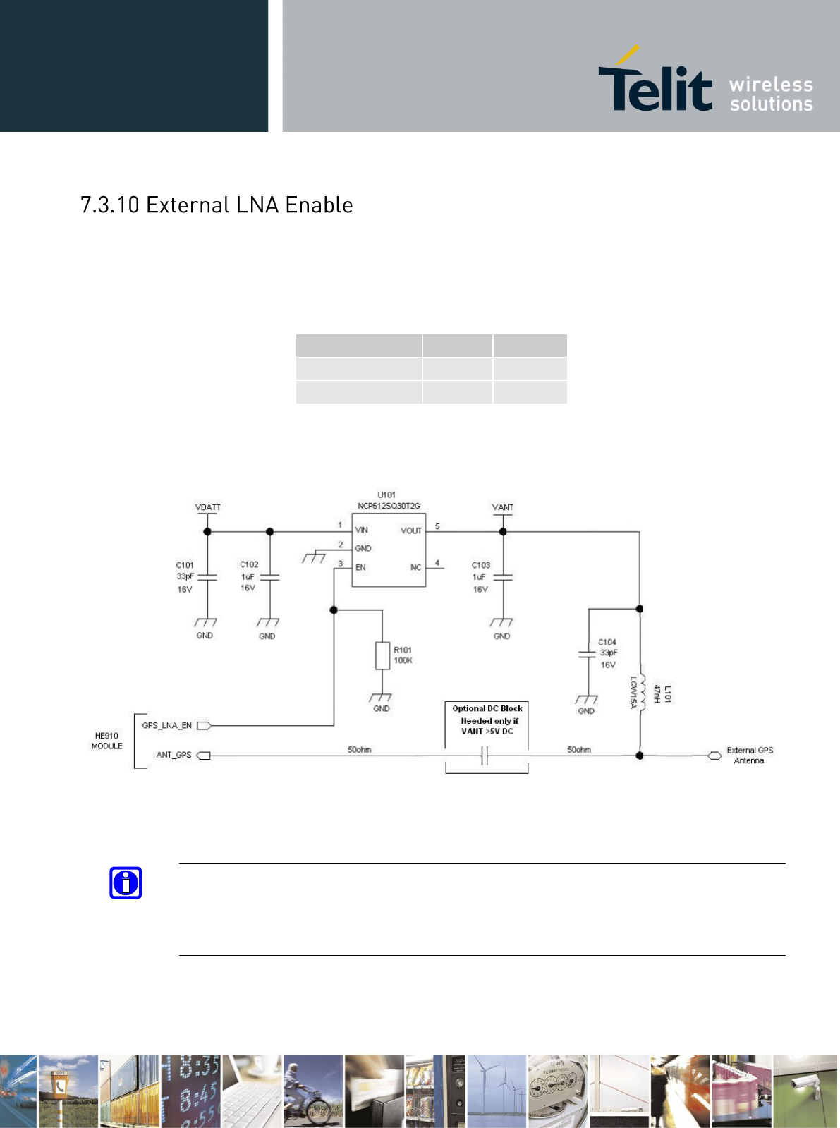
HE910 Hardware User Guide
1vv0300925 Rev.18 – 15-06-2012
Reproduction forbidden without Telit Communications S.p.A. written authorization - All Rights Reserved page 54 of 91
The HE910 is already provided by an internal LNA. In case the Application needs to include an
additional LNA stage, the module is provided by a digital signal usable to enable the power
supply of the external amplifier. The signal is set to High only when the GPS receiver is active.
The electrical characteristics of the GPS_LNA_EN signal are:
Level
Min
Max
Output high level
1.6V
1.9
Output low level
0V
0.2V
An example of GPS Antenna Supply circuit is shown in the following image:
NOTE:
The maximum DC voltage applicable to the ANT_GPS pin is 5V. In case this is exceeded, a
series capacitor has to be included in the design to avoid exceeding the maximum input DC
level.
HE910 Hardware User Guide
1vv0300925 Rev.18 – 15-06-2012
Reproduction forbidden without Telit Communications S.p.A. written authorization - All Rights Reserved page 55 of 91
Shielding the RF circuitry generally is ineffective because the interference is getting into the GPS
antenna itself, the most sensitive portion of the RF path. The antenna cannot be shielded because then
it can’t receive the GPS signals.
There are two solutions, one is to move the antenna away from the source of interference or the second
is to shield the digital interference to prevent it from getting to the antenna.
The HE910 due to its characteristics of sensitivity is capable to perform a Fix inside the
buildings. (In any case the sensitivity could be affected by the building characteristics i.e.
shielding).
The Antenna must not be co-located or operating in conjunction with any other antenna or
transmitter.
Antenna must not be installed inside metal cases.
Antenna must be installed also according to the Antenna manufacturer instructions.
HE910 Hardware User Guide
1vv0300925 Rev.18 – 15-06-2012
Reproduction forbidden without Telit Communications S.p.A. written authorization - All Rights Reserved page 56 of 91
The following table shows the logic level specifications used in the HE910 interface circuits:
Absolute Maximum Ratings -Not Functional
Parameter
Min
Max
Input level on any digital pin (CMOS 1.8) with respect
to ground
-0.3V
3.1V
Operating Range - Interface levels (1.8V CMOS)
Level
Min
Max
Input high level
1.5V
1.9V
Input low level
0V
0.35V
Output high level
1.6V
1.9
Output low level
0V
0.2V
Current characteristics (Preliminary values)
Level
Typical
Output Current
1mA
Input Current
1uA
HE910 Hardware User Guide
1vv0300925 Rev.18 – 15-06-2012
Reproduction forbidden without Telit Communications S.p.A. written authorization - All Rights Reserved page 57 of 91
The HE910 module is provided by two Reset lines that are described in the following table:
Signal
Function
I/O
PAD
HW_SHUTDOWN*
Phone Unconditional
Shut Down
I
R13
Unconditional Shutdown of the module.
It will NOT perform the detach from the
cellular network
RESET*
Phone reset
I
P11
Power-cycle of the module, but will NOT
perform the detach from the cellular network
RESET* and HW_SHUTDOWN are used to reset the HE910. Whenever those signals are
pulled low, the HE910 is reset. When the device is reset it stops any operation. After the
release of the reset HE910 is unconditionally shut down (in case of HW_SHUTDOWN*) or
restart (in case of RESET*), without doing any detach operation from the network where it
is registered. This behaviour is not a proper shut down because any GSM device is requested
to issue a detach request on turn off. For this reason the Reset signal must not be used to
normally shutting down the device, but only as an emergency exit in the rare case the device
remains stuck waiting for some network response.
The RESET* and HW_SHUTDOWN* are internally controlled on start-up to achieve always
a proper power-on reset sequence, so there's no need to control the pins on start-up. They
may only be used to reset a device already on that is not responding to any command.
NOTE:
Do not use those signals to power off the HE910. Use the ON/OFF signal to perform this
function or the AT#SHDN command.
Reset Signal Operating levels:
Signal
Min
Max
Input high
1.5V
1.9V
Input low
0V
0.35V
* this signal is internally pulled up so the pin can be left floating if not used.
If unused, this signal may be left unconnected. If used, then it must always be connected
with an open collector transistor, to permit to the internal circuitry the power on reset and
under voltage lockout functions.

HE910 Hardware User Guide
1vv0300925 Rev.18 – 15-06-2012
Reproduction forbidden without Telit Communications S.p.A. written authorization - All Rights Reserved page 58 of 91
The HE910 includes one integrated universal serial bus (USB) transceiver:
USB 2.0 HS
This port is compliant with the USB 2.0 specifications.
The following table is listing the available signals:
PAD
Signal
I/O
Function
Type
NOTE
B15
USB_D+
I/O
USB differential Data (+)
3.3V
C15
USB_D-
I/O
USB differential Data (-)
3.3V
A13
VUSB
AI
Power sense for the internal USB
transceiver.
5V
Accepted range:
4.4V to 5.25V
The USB_DPLUS and USB_DMINUS signals have a clock rate of 480 MHz. The signal
traces should be routed carefully. Trace lengths, number of vias and capacitive
loading should be minimized. The impedance value should be as close as possible to 90
Ohms differential.
HE910 Hardware User Guide
1vv0300925 Rev.18 – 15-06-2012
Reproduction forbidden without Telit Communications S.p.A. written authorization - All Rights Reserved page 59 of 91
The HE910 Module is provided by one SPI interface.
The SPI interface defines two handshake lines for flow control and mutual wake-up of the
modem and the Application Processor: SRDY (slave ready) and MRDY (master ready).
The AP has the master role, that is, it supplies the clock.
The following table is listing the available signals:
PAD
Signal
I/O
Function
Type
COMMENT
D15
SPI_MOSI
I
SPI MOSI
CMOS 1.8V
Shared with TX_AUX
E15
SPI_MISO
O
SPI MISO
CMOS 1.8V
Shared with RX_AUX
F15
SPI_CLK
I
SPI Clock
CMOS 1.8V
H15
SPI_MRDY
I
SPI_MRDY
CMOS 1.8V
J15
SPI_SRDY
O
SPI_SRDY
CMOS 1.8V
The signal 1V8_SEL must be connected to the VDD_IO1 input pin to properly supply this
digital section.
NOTE:
Due to the shared functions, when the SPI port is used, it is not possible to use the AUX_UART
port.
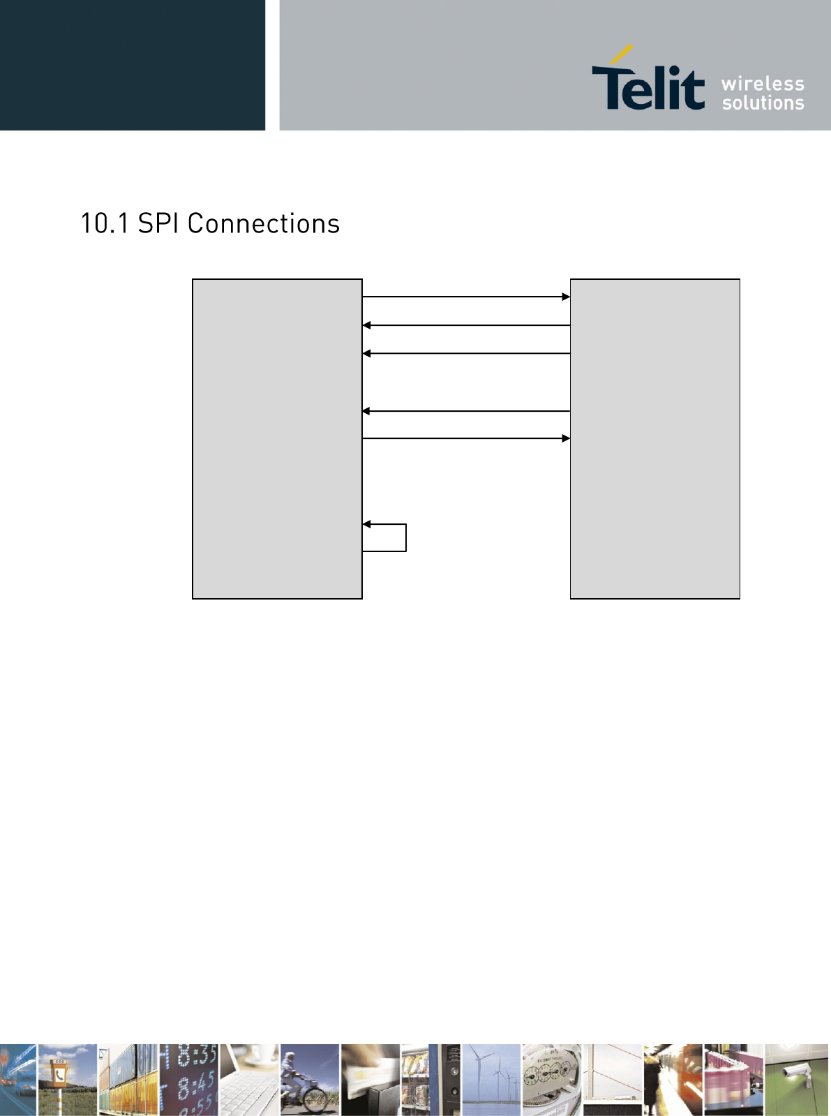
HE910 Hardware User Guide
1vv0300925 Rev.18 – 15-06-2012
Reproduction forbidden without Telit Communications S.p.A. written authorization - All Rights Reserved page 60 of 91
SPI_MISO
E15
D15
F15
H15
J15
D13
E13
D14
HE910
AP
SPI_MOSI
SPI_CLK
SPI_MRDY
SPI_SRDY
VDD_IO1
1V8_SEL
nc
HE910 Hardware User Guide
1vv0300925 Rev.18 – 15-06-2012
Reproduction forbidden without Telit Communications S.p.A. written authorization - All Rights Reserved page 61 of 91
The HE910 module is provided with by 2 Asynchronous serial ports:
MODEM SERIAL PORT 1 (Main)
MODEM SERIAL PORT 2 (Auxiliary)
Several configurations can be designed for the serial port on the OEM hardware, but the most
common are:
RS232 PC com port
microcontroller UART @ 1.8V (Universal Asynchronous Receive Transmit)
microcontroller UART @ 5V or other voltages different from 1.8V
Depending from the type of serial port on the OEM hardware a level translator circuit may be
needed to make the system work.
On the HE910 the ports are CMOS 1.8..
The electrical characteristics of the Serial ports are explained in the following tables:
Absolute Maximum Ratings -Not Functional
Parameter
Min
Max
Input level on any digital pin (CMOS 1.8) with
respect to ground
-0.3V
3.1V
Operating Range - Interface levels (1.8V CMOS)
Level
Min
Max
Input high level
1.5V
1.9V
Input low level
0V
0.35V
Output high level
1.6V
1.9
Output low level
0V
0.2V
HE910 Hardware User Guide
1vv0300925 Rev.18 – 15-06-2012
Reproduction forbidden without Telit Communications S.p.A. written authorization - All Rights Reserved page 62 of 91
The serial port 1 on the HE910 is a +1.8V UART with all the 7 RS232 signals.
It differs from the PC-RS232 in the signal polarity (RS232 is reversed) and levels.
RS232
Pin #
Signal
HE910
Pad Number
Name
Usage
1
C109/DCD
N14
Data Carrier Detect
Output from the HE910 that indicates the carrier presence
2
C104/RXD
M15
Transmit line *see
Note
Output transmit line of HE910 UART
3
C103/TXD
N15
Receive line *see
Note
Input receive of the HE910 UART
4
C108/DTR
M14
Data Terminal Ready
Input to the HE910 that controls the DTE READY condition
5
GND
M12, B13, P13,
E14 …
Ground
Ground
6
C107/DSR
P14
Data Set Ready
Output from the HE910 that indicates the module is ready
7
C106/CTS
P15
Clear to Send
Output from the HE910 that controls the Hardware flow
control
8
C105/RTS
L14
Request to Send
Input to the HE910 that controls the Hardware flow control
9
C125/RING
R14
Ring Indicator
Output from the HE910 that indicates the incoming call
condition
The following table shows the typical input value of internal pull-up resistors for RTS DTR
and TXD input lines and in all module states:
STATE
RTS DTR TXD
Pull up tied to
ON
5K to 12K
1V8
OFF
Schottky diode
RESET
Schottky diode
POWER
SAVING
5K to 12K
1V8
HE910 Hardware User Guide
1vv0300925 Rev.18 – 15-06-2012
Reproduction forbidden without Telit Communications S.p.A. written authorization - All Rights Reserved page 63 of 91
The input line ON_OFF and RESET state can be treated as in picture below
NOTE:
According to V.24, some signal names are referred to the application side, therefore on the
HE910 side these signal are on the opposite direction:
TXD on the application side will be connected to the receive line (here named C103/TXD)
RXD on the application side will be connected to the transmit line (here named C104/RXD)
NOTE:
For a minimum implementation, only the TXD, RXD lines can be connected, the other lines can
be left open provided a software flow control is implemented.
NOTE:
In order to avoid a back powering effect it is recommended to avoid having any HIGH logic
level signal applied to the digital pins of the HE910 when the module is powered off or during
an ON/OFF transition.
HE910 Hardware User Guide
1vv0300925 Rev.18 – 15-06-2012
Reproduction forbidden without Telit Communications S.p.A. written authorization - All Rights Reserved page 64 of 91
The secondary serial port on the HE910 is a CMOS1.8V with only the RX and TX
signals.
The signals of the HE910 serial port are:
PAD
Signal
I/O
Function
Type
COMMENT
D15
TX_AUX
O
Auxiliary UART (TX Data to
DTE)
CMOS 1.8V
SHARED WITH
SPI_MTSR
E15
RX_AUX
I
Auxiliary UART (RX Data from
DTE)
CMOS 1.8V
SHARED WITH
SPI_MRST
The signal 1V8_SEL must be connected to the VDD_IO1 input pin in order to use this port.
NOTE:
In order to avoid a back powering effect it is recommended to avoid having any HIGH logic
level signal applied to the digital pins of the HE910 when the module is powered off or during
an ON/OFF transition.
NOTE:
Due to the shared pins, when the Modem Serial port is used, it is not possible to use the SPI
functions.
HE910 Hardware User Guide
1vv0300925 Rev.18 – 15-06-2012
Reproduction forbidden without Telit Communications S.p.A. written authorization - All Rights Reserved page 65 of 91
In order to interface the HE910 with a PC com port or a RS232 (EIA/TIA-232) application a
level translator is required. This level translator must:
invert the electrical signal in both directions;
Change the level from 0/1.8V to +15/-15V.
Actually, the RS232 UART 16450, 16550, 16650 & 16750 chipsets accept signals with lower
levels on the RS232 side (EIA/TIA-562), allowing a lower voltage-multiplying ratio on the level
translator. Note that the negative signal voltage must be less than 0V and hence some sort of
level translation is always required.
The simplest way to translate the levels and invert the signal is by using a single chip level
translator. There are a multitude of them, differing in the number of drivers and receivers and in
the levels (be sure to get a true RS232 level translator not a RS485 or other standards).
By convention the driver is the level translator from the 0-1.8V UART to the RS232 level. The
receiver is the translator from the RS232 level to 0-1.8V UART.
In order to translate the whole set of control lines of the UART you will need:
5 drivers
3 receivers
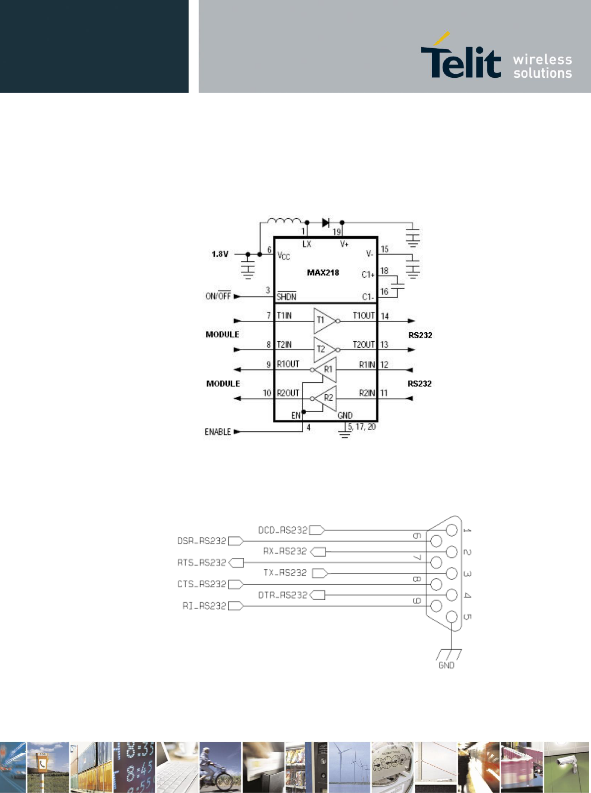
HE910 Hardware User Guide
1vv0300925 Rev.18 – 15-06-2012
Reproduction forbidden without Telit Communications S.p.A. written authorization - All Rights Reserved page 66 of 91
An example of RS232 level adaptation circuitry could be done using a MAXIM transceiver
(MAX218)
In this case the chipset is capable to translate directly from 1.8V to the RS232 levels (Example
done on 4 signals only).
The RS232 serial port lines are usually connected to a DB9 connector with the following layout:

HE910 Hardware User Guide
1vv0300925 Rev.18 – 15-06-2012
Reproduction forbidden without Telit Communications S.p.A. written authorization - All Rights Reserved page 67 of 91
The Audio of the HE910 Module is carried by DVI digital audio interface.
The audio port can be directly connected to end device using digital interface, or via one of the
several compliant codecs (in case an analog audio is needed).
The product is providing the Digital Audio Interface (DVI) on the following Pins:
Digital Voice Interface (DVI)
PAD
Signal
I/O
Function
Note
Type
B9
DVI_WA0
I/O
Digital Audio Interface (Word Alignment /
LRCLK)
CMOS 1.8V
B6
DVI_RX
I
Digital Audio Interface (RX)
CMOS 1.8V
B7
DVI_TX
O
Digital Audio Interface (TX)
CMOS 1.8V
B8
DVI_CLK
I/O
Digital Audio Interface (BCLK)
CMOS 1.8V
Please refer to the HE910 Digital Audio Application note.
HE910 Hardware User Guide
1vv0300925 Rev.18 – 15-06-2012
Reproduction forbidden without Telit Communications S.p.A. written authorization - All Rights Reserved page 68 of 91
The HE910 module is provided by a set of Digital Input / Output pins
Input pads can only be read; they report the digital value (high or low) present on the pad at the
read time.
Output pads can only be written or queried and set the value of the pad output.
An alternate function pad is internally controlled by the HE910 firmware and acts depending on
the function implemented.
The following table shows the available GPIO on the HE910:
PAD
Signal
I/O
Function
Type
Drive
strength
Default
State
Note
C8
GPIO_01
I/O
Configurable GPIO
CMOS 1.8V
0.1 mA
INPUT
Alternate function STAT
LED
C9
GPIO_02
I/O
Configurable GPIO
CMOS 1.8V
0.1 mA
INPUT
C10
GPIO_03
I/O
Configurable GPIO
CMOS 1.8V
0.1 mA
INPUT
C11
GPIO_04
I/O
Configurable GPIO
CMOS 1.8V
0.1 mA
INPUT
B14
GPIO_05
I/O
Configurable GPIO
CMOS 1.8V
0.1 mA
INPUT
C12
GPIO_06
I/O
Configurable GPIO
CMOS 1.8V
0.1 mA
INPUT
C13
GPIO_07
I/O
Configurable GPIO
CMOS 1.8V
0.1 mA
INPUT
K15
GPIO_08
I/O
Configurable GPIO
CMOS 1.8V
0.1 mA
INPUT
VDD_IO1 has to be
connected to 1V8_SEL
L15
GPIO_09
I/O
Configurable GPIO
CMOS 1.8V
0.1 mA
INPUT
VDD_IO1 has to be
connected to 1V8_SEL
G15
GPIO_10
I/O
Configurable GPIO
CMOS 1.8V
0.1 mA
INPUT
VDD_IO1 has to be
connected to 1V8_SEL
HE910 Hardware User Guide
1vv0300925 Rev.18 – 15-06-2012
Reproduction forbidden without Telit Communications S.p.A. written authorization - All Rights Reserved page 69 of 91
Where not specifically stated, all the interface circuits work at 1.8V CMOS logic levels.
The following table shows the logic level specifications used in the HE910 interface circuits:
Absolute Maximum Ratings -Not Functional
Parameter
Min
Max
Input level on any digital pin (CMOS 1.8) with respect
to ground
-0.3V
3.1V
Operating Range - Interface levels (1.8V CMOS)
Level
Min
Max
Input high level
1.5V
1.9V
Input low level
0V
0.35V
Output high level
1.6V
1.9
Output low level
0V
0.2V
HE910 Hardware User Guide
1vv0300925 Rev.18 – 15-06-2012
Reproduction forbidden without Telit Communications S.p.A. written authorization - All Rights Reserved page 70 of 91
The GPIO pads, when used as inputs, can be connected to a digital output of another device and
report its status, provided this device has interface levels compatible with the 1.8V CMOS levels
of the GPIO.
If the digital output of the device to be connected with the GPIO input pad has interface levels
different from the 1.8V CMOS, then it can be buffered with an open collector transistor with a
47K pull up to 1.8V.
NOTE:
In order to avoid a back powering effect it is recommended to avoid having any HIGH logic
level signal applied to the digital pins of the HE910 when the module is powered off or during
an ON/OFF transition.
The GPIO pads, when used as outputs, can drive 1.8V CMOS digital devices or compatible
hardware. When set as outputs, the pads have a push-pull output and therefore the pull-up
resistor may be omitted.
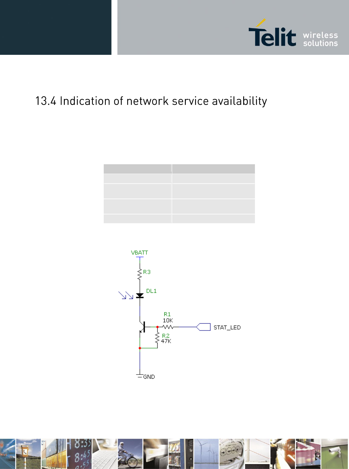
HE910 Hardware User Guide
1vv0300925 Rev.18 – 15-06-2012
Reproduction forbidden without Telit Communications S.p.A. written authorization - All Rights Reserved page 71 of 91
The STAT_LED pin status shows information on the network service availability and Call
status. The function is available as alternate function of GPIO_01
In the HE910 modules, the STAT_LED needs an external transistor to drive an external LED.
Therefore, the status indicated in the following table is reversed with respect to the pin status.
LED status
Device Status
Permanently off
Device off
Fast blinking
(Period 1s, Ton 0,5s)
Net search / Not registered /
turning off
Slow blinking
(Period 3s, Ton 0,3s)
Registered full service
Permanently on
a call is active
A schematic example could be:
HE910 Hardware User Guide
1vv0300925 Rev.18 – 15-06-2012
Reproduction forbidden without Telit Communications S.p.A. written authorization - All Rights Reserved page 72 of 91
The VRTC pin brings out the Real Time Clock supply, which is separate from the rest of the
digital part, allowing having only RTC going on when all the other parts of the device are off.
To this power output a backup capacitor can be added in order to increase the RTC autonomy
during power off of the battery. NO Devices must be powered from this pin.
Please refer to the related User Guide (SIM Holder Design Guides, 80000NT10001a).
A regulated power supply output is provided in order to supply small devices from the module.
The signal is present on Pad R11 and it is in common with the PWRMON (module powered ON
indication) function.
This output is always active when the module is powered ON.
The operating range characteristics of the supply are:
Level
Min
Typical
Max
Output voltage
1.78V
1.80V
1.82V
Output current
-
-
60mA
Output bypass capacitor
(inside the module)
1uF
HE910 Hardware User Guide
1vv0300925 Rev.18 – 15-06-2012
Reproduction forbidden without Telit Communications S.p.A. written authorization - All Rights Reserved page 73 of 91
The HE910 is provided by one AD converter. It is able to read a voltage level in the range of
0÷1.2 volts applied on the ADC pin input, store and convert it into 10 bit word.
The following table is showing the ADC characteristics:
Min
Typical
Max
Units
Input Voltage range
0
-
1.2
Volt
AD conversion
-
-
10
bits
Input Resistance
1
-
-
Mohm
Input Capacitance
-
1
-
pF
The input line is named as ADC_IN1 and it is available on Pad B1
An AT command is available to use the ADC function.
The command is AT#ADC=1,2
The read value is expressed in mV
Refer to SW User Guide or AT Commands Reference Guide for the full description of this
function.
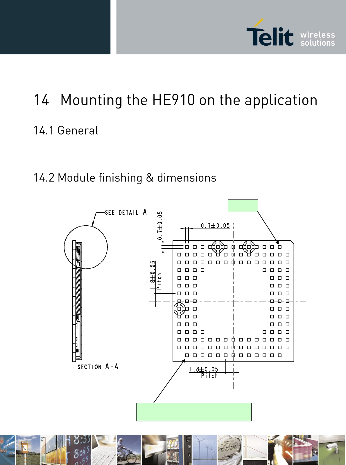
HE910 Hardware User Guide
1vv0300925 Rev.18 – 15-06-2012
Reproduction forbidden without Telit Communications S.p.A. written authorization - All Rights Reserved page 74 of 91
The HE910 modules have been designed in order to be compliant with a standard lead-free
SMT process.
Pin B1
Dimensions in mm
Bottom view
Lead-free Alloy:
Surface finishing Ni/Au for all solder pads
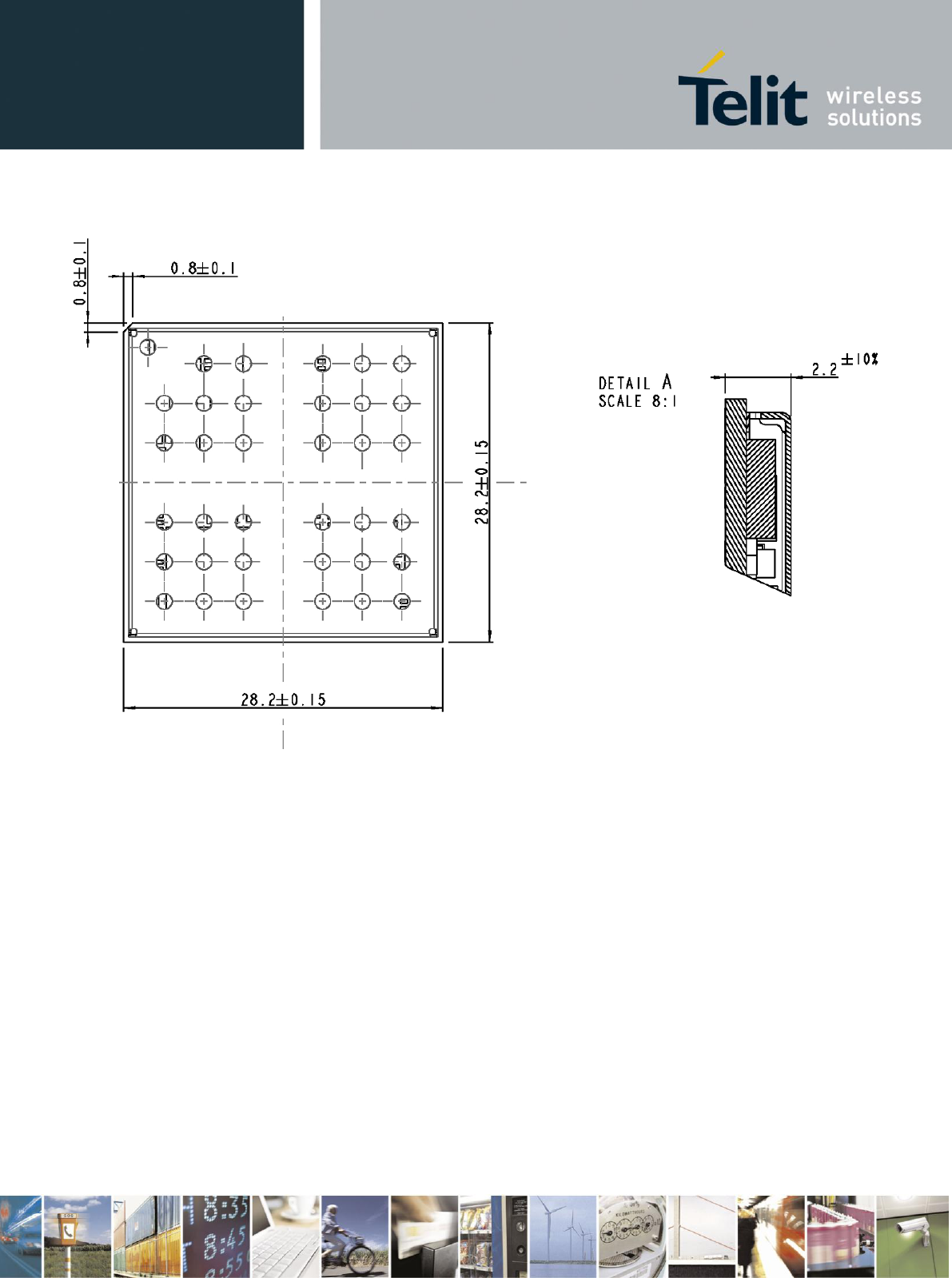
HE910 Hardware User Guide
1vv0300925 Rev.18 – 15-06-2012
Reproduction forbidden without Telit Communications S.p.A. written authorization - All Rights Reserved page 75 of 91
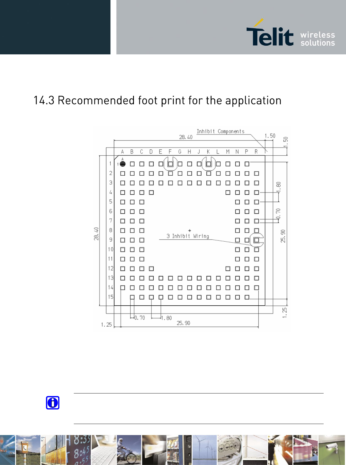
HE910 Hardware User Guide
1vv0300925 Rev.18 – 15-06-2012
Reproduction forbidden without Telit Communications S.p.A. written authorization - All Rights Reserved page 76 of 91
TOP VIEW
In order to easily rework the HE910 is suggested to consider on the application a 1.5 mm
placement inhibit area around the module.
It is also suggested, as common rule for an SMT component, to avoid having a mechanical
part of the application in direct contact with the module.
NOTE:
In the customer application, the region under WIRING INHIBIT (see figure above) must
be clear from signal or ground paths.
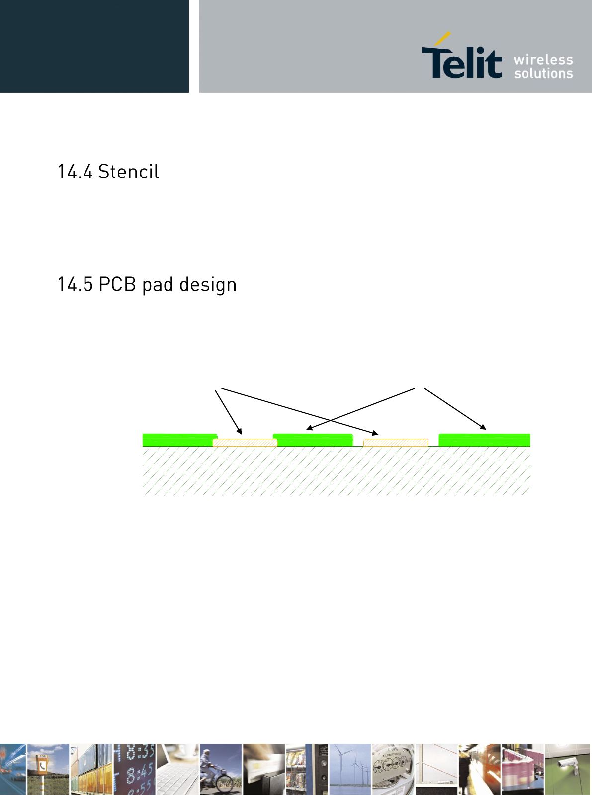
HE910 Hardware User Guide
1vv0300925 Rev.18 – 15-06-2012
Reproduction forbidden without Telit Communications S.p.A. written authorization - All Rights Reserved page 77 of 91
Stencil’s apertures layout can be the same of the recommended footprint (1:1), we
suggest a thickness of stencil foil ≥ 120 µm.
Non solder mask defined (NSMD) type is recommended for the solder pads on the
PCB.
PCB
Copper Pad
Solder Mask
SMD
(Solder Mask Defined)
NSMD
(Non Solder Mask Defined)
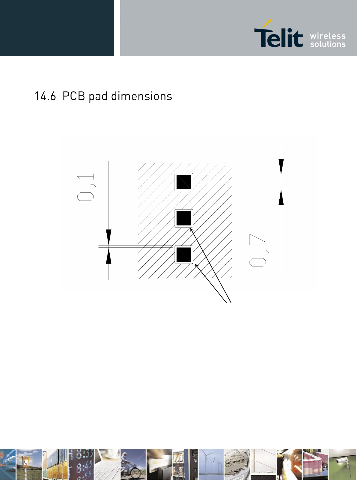
HE910 Hardware User Guide
1vv0300925 Rev.18 – 15-06-2012
Reproduction forbidden without Telit Communications S.p.A. written authorization - All Rights Reserved page 78 of 91
The recommendation for the PCB pads dimensions are described in the following image
(dimensions in mm)
Solder resist openings
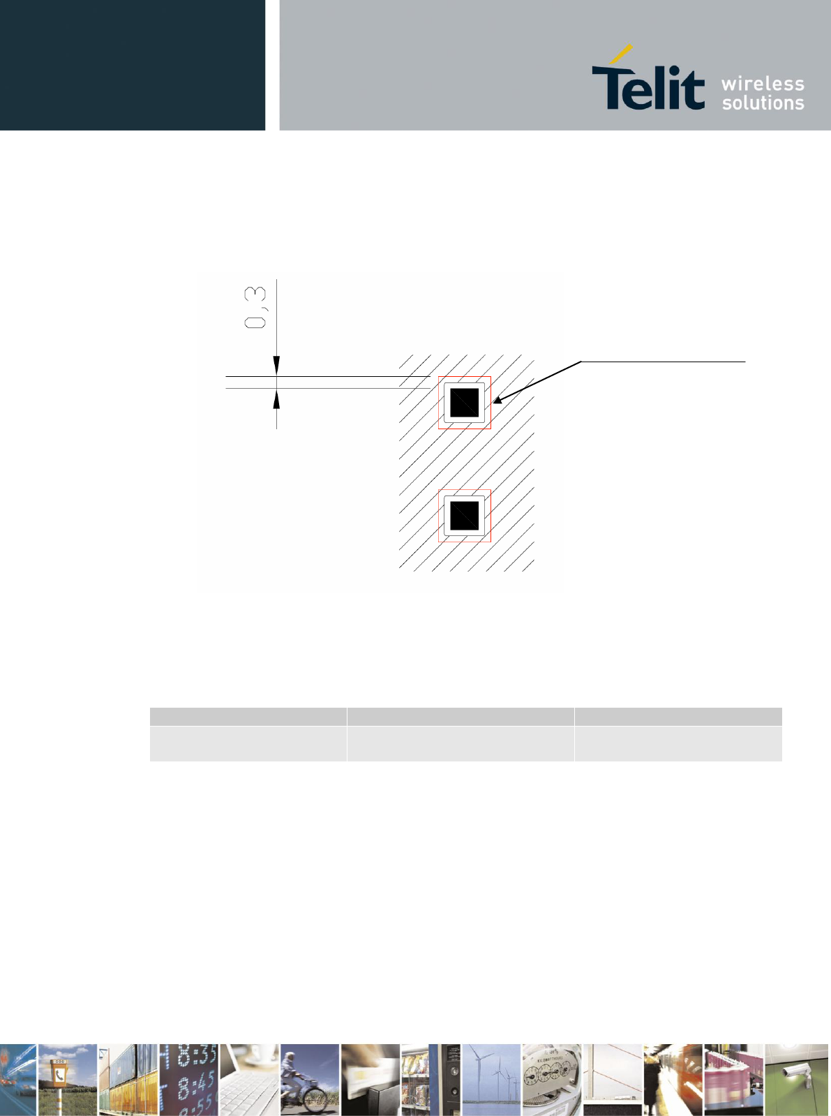
HE910 Hardware User Guide
1vv0300925 Rev.18 – 15-06-2012
Reproduction forbidden without Telit Communications S.p.A. written authorization - All Rights Reserved page 79 of 91
It is not recommended to place via or micro-via not covered by solder resist in an
area of 0,3 mm around the pads unless it carries the same signal of the pad itself
(see following figure).
Holes in pad are allowed only for blind holes and not for through holes.
Recommendations for PCB pad surfaces:
Finish
Layer thickness [µm]
Properties
Electro-less Ni / Immersion
Au
3 –7 / 0.05 – 0.15
good solder ability protection,
high shear force values
The PCB must be able to resist the higher temperatures which are occurring at the
lead-free process. This issue should be discussed with the PCB-supplier. Generally,
the wettability of tin-lead solder paste on the described surface plating is better
compared to lead-free solder paste.
It is not necessary to panel the application’s PCB, however in that case it is
suggested to use milled contours and predrilled board breakouts; scoring or v-cut
solutions are not recommended.
Inhibit area for micro-via
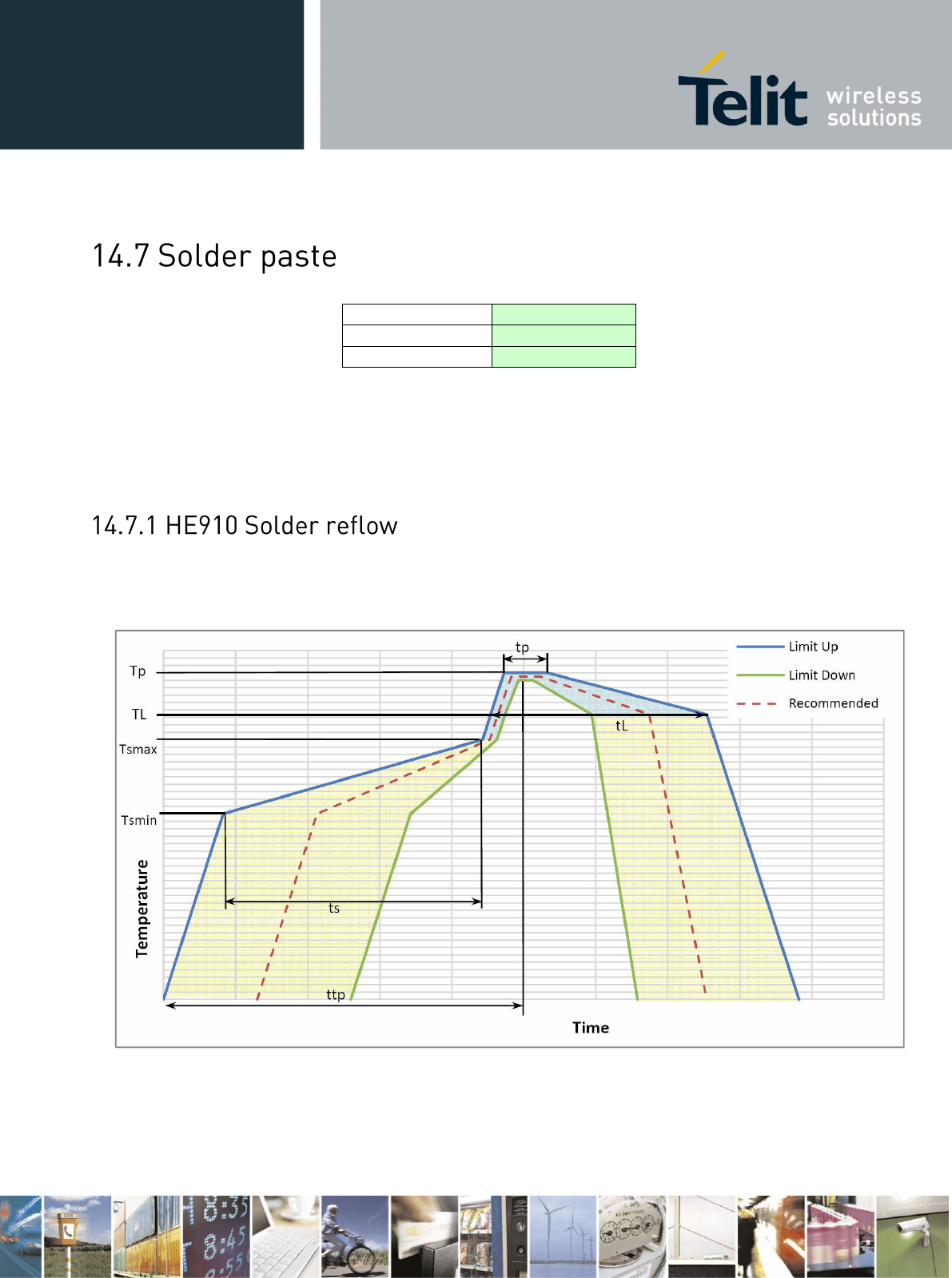
HE910 Hardware User Guide
1vv0300925 Rev.18 – 15-06-2012
Reproduction forbidden without Telit Communications S.p.A. written authorization - All Rights Reserved page 80 of 91
Lead free
Solder paste
Sn/Ag/Cu
We recommend using only “no clean” solder paste in order to avoid the cleaning of the modules
after assembly.
Recommended solder reflow profile:

HE910 Hardware User Guide
1vv0300925 Rev.18 – 15-06-2012
Reproduction forbidden without Telit Communications S.p.A. written authorization - All Rights Reserved page 81 of 91
Profile Feature
Pb-Free Assembly
Average ramp-up rate (TL to TP)
3°C/second max
Preheat
– Temperature Min (Tsmin)
– Temperature Max (Tsmax)
– Time (min to max) (ts)
150°C
200°C
60-180 seconds
Tsmax to TL
– Ramp-up Rate
3°C/second max
Time maintained above:
– Temperature (TL)
– Time (tL)
217°C
60-150 seconds
Peak Temperature (Tp)
245 +0/-5°C
Time within 5°C of actual Peak
Temperature (tp)
10-30 seconds
Ramp-down Rate
6°C/second max.
Time 25°C to Peak Temperature
8 minutes max.
NOTE:
All temperatures refer to topside of the package, measured on the package body surface
WARNING:
The HE910 module withstands one reflow process only.
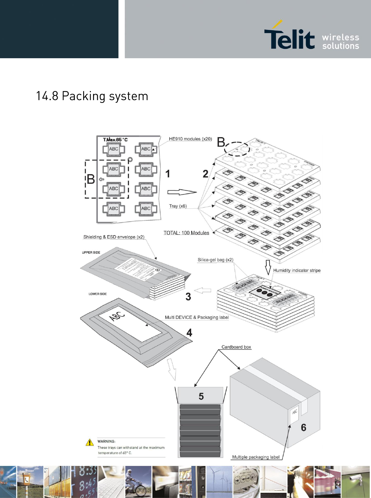
HE910 Hardware User Guide
1vv0300925 Rev.18 – 15-06-2012
Reproduction forbidden without Telit Communications S.p.A. written authorization - All Rights Reserved page 82 of 91
The HE910 modules are packaged on trays of 20 pieces each. These trays can be used in
SMT processes for pick & place handling.
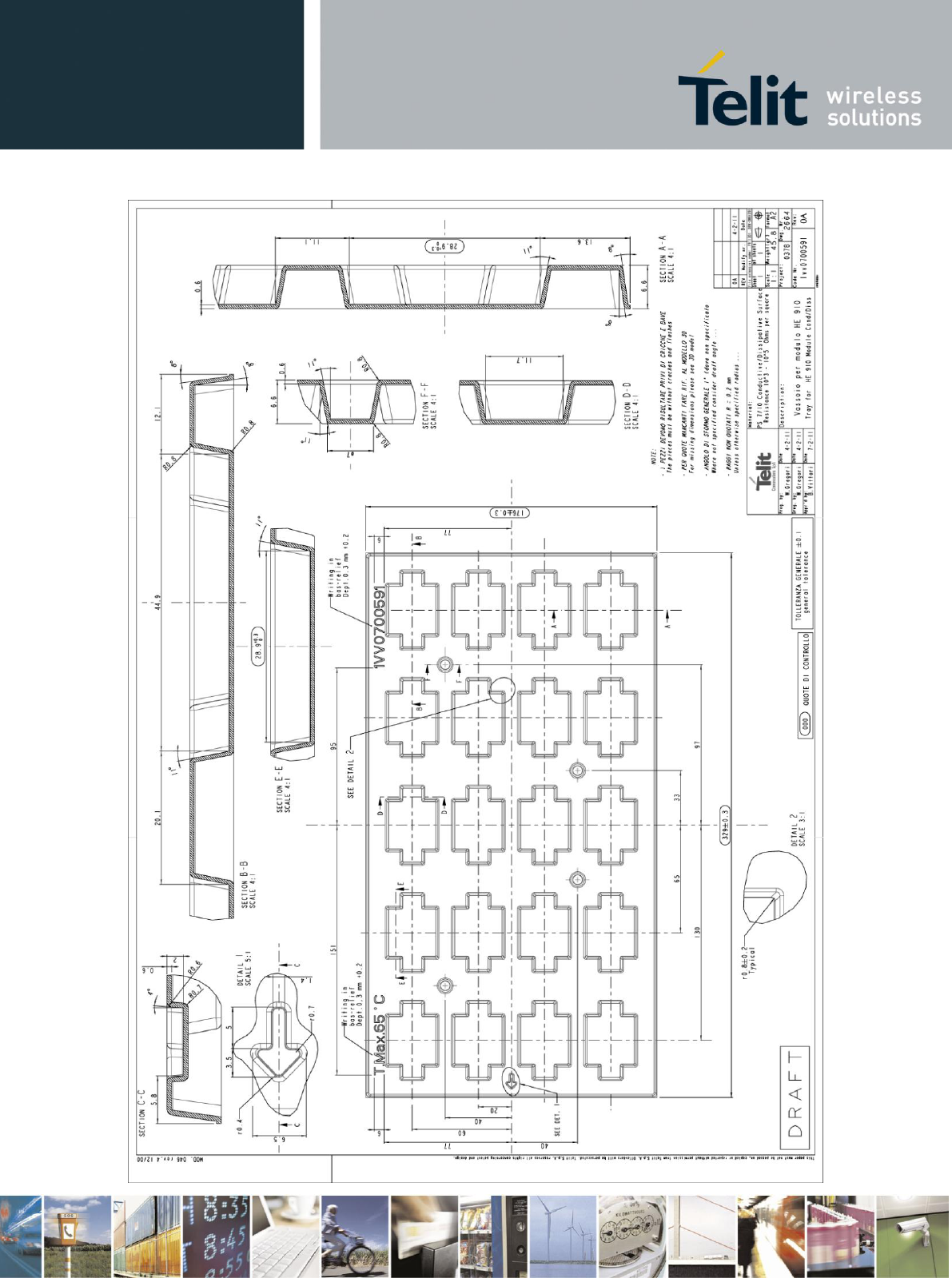
HE910 Hardware User Guide
1vv0300925 Rev.18 – 15-06-2012
Reproduction forbidden without Telit Communications S.p.A. written authorization - All Rights Reserved page 83 of 91
HE910 Hardware User Guide
1vv0300925 Rev.18 – 15-06-2012
Reproduction forbidden without Telit Communications S.p.A. written authorization - All Rights Reserved page 84 of 91
The HE910 is a Moisture Sensitive Device level 3, in according with standard IPC/JEDEC J-
STD-020, take care all the relatives requirements for using this kind of components.
Moreover, the customer has to take care of the following conditions:
a) Calculated shelf life in sealed bag: 12 months at <40°C and <90% relative humidity (RH).
b) Environmental condition during the production: 30°C / 60% RH according to IPC/JEDEC
J-STD-033A paragraph 5.
c) The maximum time between the opening of the sealed bag and the reflow process must be
168 hours if condition b) “IPC/JEDEC J-STD-033A paragraph 5.2” is respected
d) Baking is required if conditions b) or c) are not respected
e) Baking is required if the humidity indicator inside the bag indicates 10% RH
or more
HE910 Hardware User Guide
1vv0300925 Rev.18 – 15-06-2012
Reproduction forbidden without Telit Communications S.p.A. written authorization - All Rights Reserved page 85 of 91
READ CAREFULLY
Be sure the use of this product is allowed in the country and in the environment required. The use of this
product may be dangerous and has to be avoided in the following areas:
Where it can interfere with other electronic devices in environments such as hospitals, airports,
aircrafts, etc
Where there is risk of explosion such as gasoline stations, oil refineries, etc
It is responsibility of the user to enforce the country regulation and the specific environment regulation.
Do not disassemble the product; any mark of tampering will compromise the warranty validity.
We recommend following the instructions of the hardware user guides for a correct wiring of the product.
The product has to be supplied with a stabilized voltage source and the wiring has to be conforming to the
security and fire prevention regulations.
The product has to be handled with care, avoiding any contact with the pins because electrostatic
discharges may damage the product itself. Same cautions have to be taken for the SIM, checking carefully
the instruction for its use. Do not insert or remove the SIM when the product is in power saving mode.
The system integrator is responsible of the functioning of the final product; therefore, care has to be taken
to the external components of the module, as well as of any project or installation issue, because the risk
of disturbing the GSM network or external devices or having impact on the security. Should there be any
doubt, please refer to the technical documentation and the regulations in force.
Every module has to be equipped with a proper antenna with specific characteristics. The antenna has to
be installed with care in order to avoid any interference with other electronic devices and has to guarantee
a minimum distance from the body (20 cm). In case of this requirement cannot be satisfied, the system
integrator has to assess the final product against the SAR regulation.
The European Community provides some Directives for the electronic equipments introduced on the
market. All the relevant information’s are available on the European Community website:
http://europa.eu.int/comm/enterprise/rtte/dir99-5.htm
The text of the Directive 99/05 regarding telecommunication equipments is available, while the applicable
Directives (Low Voltage and EMC) are available at:
http://europa.eu.int/comm/enterprise/electr_equipment/index_en.htm
HE910 Hardware User Guide
1vv0300925 Rev.18 – 15-06-2012
Reproduction forbidden without Telit Communications S.p.A. written authorization - All Rights Reserved page 86 of 91
The HE910, HE910-D, HE910-GA, HE910-EUG, HE910-EUR, HE910-EUD, HE910-NAG, HE910-
NAR, HE910-NAD modules have been evaluated against the essential requirements of the 1999/5/EC
Directive.
Bulgarian
С настоящето Telit Communications S.p.A. декларира, че 2G/3G module отговаря на
съществените изисквания и другите приложими изисквания на Директива
1999/5/ЕС.
Czech
Telit Communications S.p.A. tímto prohlašuje, že tento 2G/3G module je ve shodě se
základními požadavky a dalšími příslušnými ustanoveními směrnice 1999/5/ES.
Danish
Undertegnede Telit Communications S.p.A. erklærer herved, at følgende udstyr 2G/3G
module overholder de væsentlige krav og øvrige relevante krav i direktiv 1999/5/EF.
Dutch
Hierbij verklaart Telit Communications S.p.A. dat het toestel 2G/3G module in
overeenstemming is met de essentiële eisen en de andere relevante bepalingen van
richtlijn 1999/5/EG.
English
Hereby, Telit Communications S.p.A., declares that this 2G/3G module is in compliance
with the essential requirements and other relevant provisions of Directive 1999/5/EC.
Estonian
Käesolevaga kinnitab Telit Communications S.p.A. seadme 2G/3G module vastavust
direktiivi 1999/5/EÜ põhinõuetele ja nimetatud direktiivist tulenevatele teistele
asjakohastele sätetele.
German
Hiermit erklärt Telit Communications S.p.A., dass sich das Gerät 2G/3G module in
Übereinstimmung mit den grundlegenden Anforderungen und den übrigen einschlägigen
Bestimmungen der Richtlinie 1999/5/EG befindet.
Greek
ΜΕ ΣΗΝ ΠΑΡΟΤΑ Telit Communications S.p.A. ΔΗΛΩΝΕΙ ΟΣΙ 2G/3G module
ΤΜΜΟΡΦΩΝΕΣΑΙ ΠΡΟ ΣΙ ΟΤΙΩΔΕΙ ΑΠΑΙΣΗΕΙ ΚΑΙ ΣΙ ΛΟΙΠΕ ΥΕΣΙΚΕ
ΔΙΑΣΑΞΕΙ ΣΗ ΟΔΗΓΙΑ 1999/5/ΕΚ.
Hungarian
Alulírott, Telit Communications S.p.A. nyilatkozom, hogy a 2G/3G module megfelel a
vonatkozó alapvetõ követelményeknek és az 1999/5/EC irányelv egyéb elõírásainak.
Finnish
Telit Communications S.p.A. vakuuttaa täten että 2G/3G module tyyppinen laite on
direktiivin 1999/5/EY oleellisten vaatimusten ja sitä koskevien direktiivin muiden ehtojen
mukainen.
French
Par la présente Telit Communications S.p.A. déclare que l'appareil 2G/3G module est
conforme aux exigences essentielles et aux autres dispositions pertinentes de la
directive 1999/5/CE.
Icelandic
Hér með lýsir Telit Communications S.p.A. yfir því að 2G/3G module er í samræmi við
grunnkröfur og aðrar kröfur, sem gerðar eru í tilskipun 1999/5/EC
Italian
Con la presente Telit Communications S.p.A. dichiara che questo 2G/3G module è
conforme ai requisiti essenziali ed alle altre disposizioni pertinenti stabilite dalla direttiva
1999/5/CE.

HE910 Hardware User Guide
1vv0300925 Rev.18 – 15-06-2012
Reproduction forbidden without Telit Communications S.p.A. written authorization - All Rights Reserved page 87 of 91
Latvian
Ar šo Telit Communications S.p.A. deklarē, ka 2G/3G module atbilst Direktīvas
1999/5/EK būtiskajām prasībām un citiem ar to saistītajiem noteikumiem.
Lithuanian
Šiuo Telit Communications S.p.A. deklaruoja, kad šis 2G/3G module atitinka esminius
reikalavimus ir kitas 1999/5/EB Direktyvos nuostatas.
Maltese
Hawnhekk, Telit Communications S.p.A., jiddikjara li dan 2G/3G module jikkonforma
mal-ħtiġijiet essenzjali u ma provvedimenti oħrajn relevanti li hemm fid-Dirrettiva
1999/5/EC.
Norwegian
Telit Communications S.p.A. erklærer herved at utstyret 2G/3G module er i samsvar
med de grunnleggende krav og øvrige relevante krav i direktiv 1999/5/EF.
Polish
Niniejszym Telit Communications S.p.A. oświadcza, że 2G/3G module jest zgodny z
zasadniczymi wymogami oraz pozostałymi stosownymi postanowieniami Dyrektywy
1999/5/EC
Portuguese
Telit Communications S.p.A. declara que este 2G/3G module está conforme com os
requisitos essenciais e outras disposições da Directiva 1999/5/CE.
Slovak
Telit Communications S.p.A. týmto vyhlasuje, že 2G/3G module spĺňa základné
požiadavky a všetky príslušné ustanovenia Smernice 1999/5/ES.
Slovenian
Telit Communications S.p.A. izjavlja, da je ta 2G/3G module v skladu z bistvenimi
zahtevami in ostalimi relevantnimi določili direktive 1999/5/ES.
Spanish
Por medio de la presente Telit Communications S.p.A. declara que el 2G/3G module
cumple con los requisitos esenciales y cualesquiera otras disposiciones aplicables o
exigibles de la Directiva 1999/5/CE.
Swedish
Härmed intygar Telit Communications S.p.A. att denna 2G/3G module står I
överensstämmelse med de väsentliga egenskapskrav och övriga relevanta
bestämmelser som framgår av direktiv 1999/5/EG.
In order to satisfy the essential requirements of 1999/5/EC Directive, the HE910,
HE910-GA, HE910-EUG modules are compliant with the following standards:
RF spectrum use (R&TTE art. 3.2)
EN 300 440-2 V1.4.1
EN 301 511 V9.0.2
EN 301 908-1 V4.2.1
EN 301 908-2 V4.2.1
EMC (R&TTE art. 3.1b)
EN 301 489-1 V1.8.1
EN 301 489-3 V1.4.1
EN 301 489-7 V1.3.1
EN 301 489-24 V1.5.1
Health & Safety (R&TTE art. 3.1a)
EN 60950-1:2006 + A11:2009 + A1:2010 + A12:2011
In order to satisfy the essential requirements of 1999/5/EC Directive, the HE910-NAG modules are
compliant with the following standards:
RF spectrum use (R&TTE art. 3.2)
EN 300 440-2 V1.4.1
EN 301 511 V9.0.2
EMC (R&TTE art. 3.1b)
EN 301 489-1 V1.8.1
EN 301 489-3 V1.4.1
EN 301 489-7 V1.3.1
Health & Safety (R&TTE art. 3.1a)
EN 60950-1:2006 + A11:2009 + A1:2010 + A12:2011
HE910 Hardware User Guide
1vv0300925 Rev.18 – 15-06-2012
Reproduction forbidden without Telit Communications S.p.A. written authorization - All Rights Reserved page 88 of 91
The HE910-D, HE910-EUR, HE910-EUD modules are compliant with the following standards:
RF spectrum use (R&TTE art. 3.2)
EN 301 511 V9.02
EN 301 908-1 V4.2.1
EN 301 908-2 V4.2.1
EMC (R&TTE art. 3.1b)
EN 301 489-1 V1.8.1
EN 301 489-7 V1.3.1
EN 301 489-24 V1.5.1
Health & Safety (R&TTE art. 3.1a)
EN 60950-1:2006 + A11:2009 + A1:2010 + A12:2011
The HE910-NAR, HE910-NAD modules are compliant with the following standards:
RF spectrum use (R&TTE art. 3.2)
EN 301 511 V9.02
EMC (R&TTE art. 3.1b)
EN 301 489-1 V1.8.1
EN 301 489-7 V1.3.1
Health & Safety (R&TTE art. 3.1a)
EN 60950-1:2006 + A11:2009 + A1:2010 + A12:2011
The conformity assessment procedure referred to in Article 10 and detailed in Annex IV of Directive
1999/5/EC has been followed with the involvement of the following Notified Body:
AT4 wireless, S.A.
Parque Tecnologico de Andalucía
C/ Severo Ochoa 2
29590 Campanillas – Málaga
SPAIN
Notified Body No: 1909
Thus, the following marking is included in the product:
The full declaration of conformity can be found on the following address:
http://www.telit.com/
There is no restriction for the commercialisation of the HE910, HE910-D, HE910-GA, HE910-EUG,
HE910-EUR, HE910-EUD, HE910-NAG, HE910-NAR, HE910-NAD modules in all the countries of the
European Union.
1909

HE910 Hardware User Guide
1vv0300925 Rev.18 – 15-06-2012
Reproduction forbidden without Telit Communications S.p.A. written authorization - All Rights Reserved page 89 of 91
Final product integrating this module must be assessed against essential requirements of the 1999/5/EC
(R&TTE) Directive. It should be noted that assessment does not necessarily lead to testing. Telit
Communications S.p.A. recommends carrying out the following assessments:
RF spectrum use (R&TTE art. 3.2)
It will depend on the antenna used on the final product.
EMC (R&TTE art. 3.1b)
Testing
Health & Safety (R&TTE art. 3.1a)
Testing
Alternately, assessment of the final product against EMC (Art. 3.1b) and Electrical safety (Art. 3.1a)
essential requirements can be done against the essential requirements of the EMC and the LVD Directives:
Low Voltage Directive 2006/95/EC and product safety
Directive EMC 2004/108/EC for conformity for EMC
HE910 Hardware User Guide
1vv0300925 Rev.18 – 15-06-2012
Reproduction forbidden without Telit Communications S.p.A. written authorization - All Rights Reserved page 90 of 91
Modification statement
Telit has not approved any changes or modifications to this device by the user. Any changes or modifications
could void the user’s authority to operate the equipment.
Telit n’approuve aucune modification apportée à l’appareil par l’utilisateur, quelle qu’en soit la nature. Tout
changement ou modification peuvent annuler le droit d’utilisation de l’appareil par l’utilisateur.
Interference statement
This device complies with Part 15 of the FCC Rules and Industry Canada licence-exempt RSS standard(s).
Operation is subject to the following two conditions: (1) this device may not cause interference, and (2) this
device must accept any interference, including interference that may cause undesired operation of the device.
Le présent appareil est conforme aux CNR d'Industrie Canada applicables aux appareils radio exempts de
licence. L'exploitation est autorisée aux deux conditions suivantes : (1) l'appareil ne doit pas produire de
brouillage, et (2) l'utilisateur de l'appareil doit accepter tout brouillage radioélectrique subi, même si le
brouillage est susceptible d'en compromettre le fonctionnement.
Wireless notice
This equipment complies with FCC and IC radiation exposure limits set forth for an uncontrolled environment.
The antenna should be installed and operated with minimum distance of 20 cm between the radiator and your
body. Antenna gain must be below:
Frequency band
HE910, HE910-D
HE910-GA
HE910-NAR, HE910-NAD, HE910-NAG
GSM 850/FDD V
5.22 dBi
5.22 dBi
5.29 dBi
PCS 1900/FDD II
3.31 dBi
3.31 dBi
4.02 dBi
FDD IV
6.45 dBi
6.32 dBi
This transmitter must not be co-located or operating in conjunction with any other antenna or transmitter.

HE910 Hardware User Guide
1vv0300925 Rev.18 – 15-06-2012
Reproduction forbidden without Telit Communications S.p.A. written authorization - All Rights Reserved page 91 of 91
Cet appareil est conforme aux limites d'exposition aux rayonnements de la IC pour un environnement non
contrôlé. L'antenne doit être installé de façon à garder une distance minimale de 20 centimètres entre la source
de rayonnements et votre corps. Gain de l'antenne doit être ci-dessous:
Bande de fréquence
HE910, HE910-D
HE910-GA
HE910-NAR, HE910-NAD, HE910-NAG
GSM 850/FDD V
5.22 dBi
5.22 dBi
5.29 dBi
PCS 1900/FDD II
3.31 dBi
3.31 dBi
4.02 dBi
FDD IV
6.45 dBi
6.32 dBi
L'émetteur ne doit pas être colocalisé ni fonctionner conjointement avec à autre antenne ou autre émetteur.
FCC Class B digital device notice
This equipment has been tested and found to comply with the limits for a Class B digital device, pursuant to part
15 of the FCC Rules. These limits are designed to provide reasonable protection against harmful interference in a
residential installation. This equipment generates, uses and can radiate radio frequency energy and, if not
installed and used in accordance with the instructions, may cause harmful interference to radio communications.
However, there is no guarantee that interference will not occur in a particular installation. If this equipment does
cause harmful interference to radio or television reception, which can be determined by turning the equipment
off and on, the user is encouraged to try to correct the interference by one or more of the following measures:
- Reorient or relocate the receiving antenna.
- Increase the separation between the equipment and receiver.
- Connect the equipment into an outlet on a circuit different from that to which the receiver is connected.
- Consult the dealer or an experienced radio/TV technician for help.