Telit Communications S p A LN930 DATA CARD User Manual xN930 M 2 Hardware User Guide
Telit Communications S.p.A. DATA CARD xN930 M 2 Hardware User Guide
UserManual.wiki
>
Telit Communications S p A
>
LN930 User Manual
User Manual
Navigation menu
Upload a User Manual
Namespaces
Wiki Guide
HTML
PDF
Info
Views
User Manual
Discussion / Help
Navigation
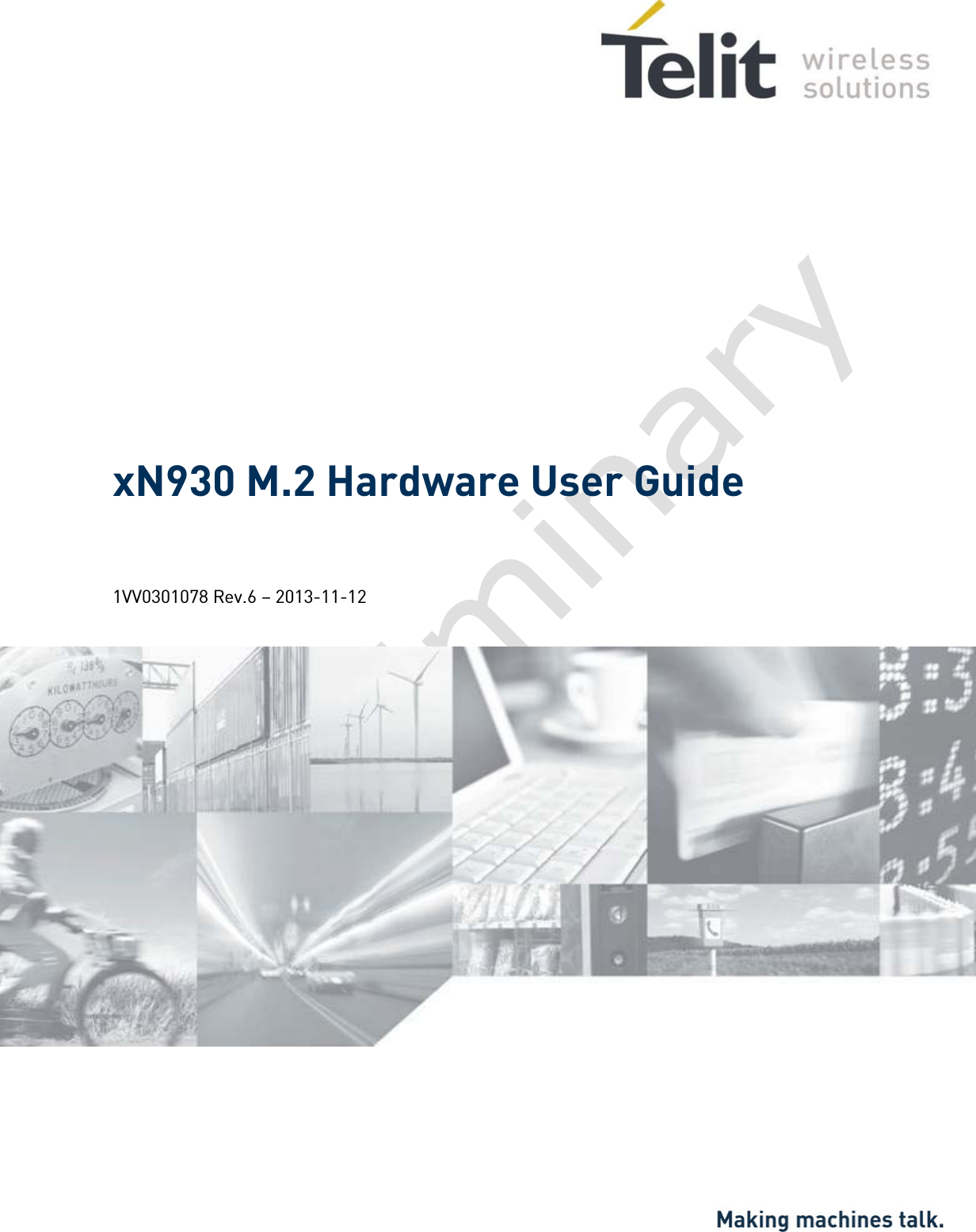
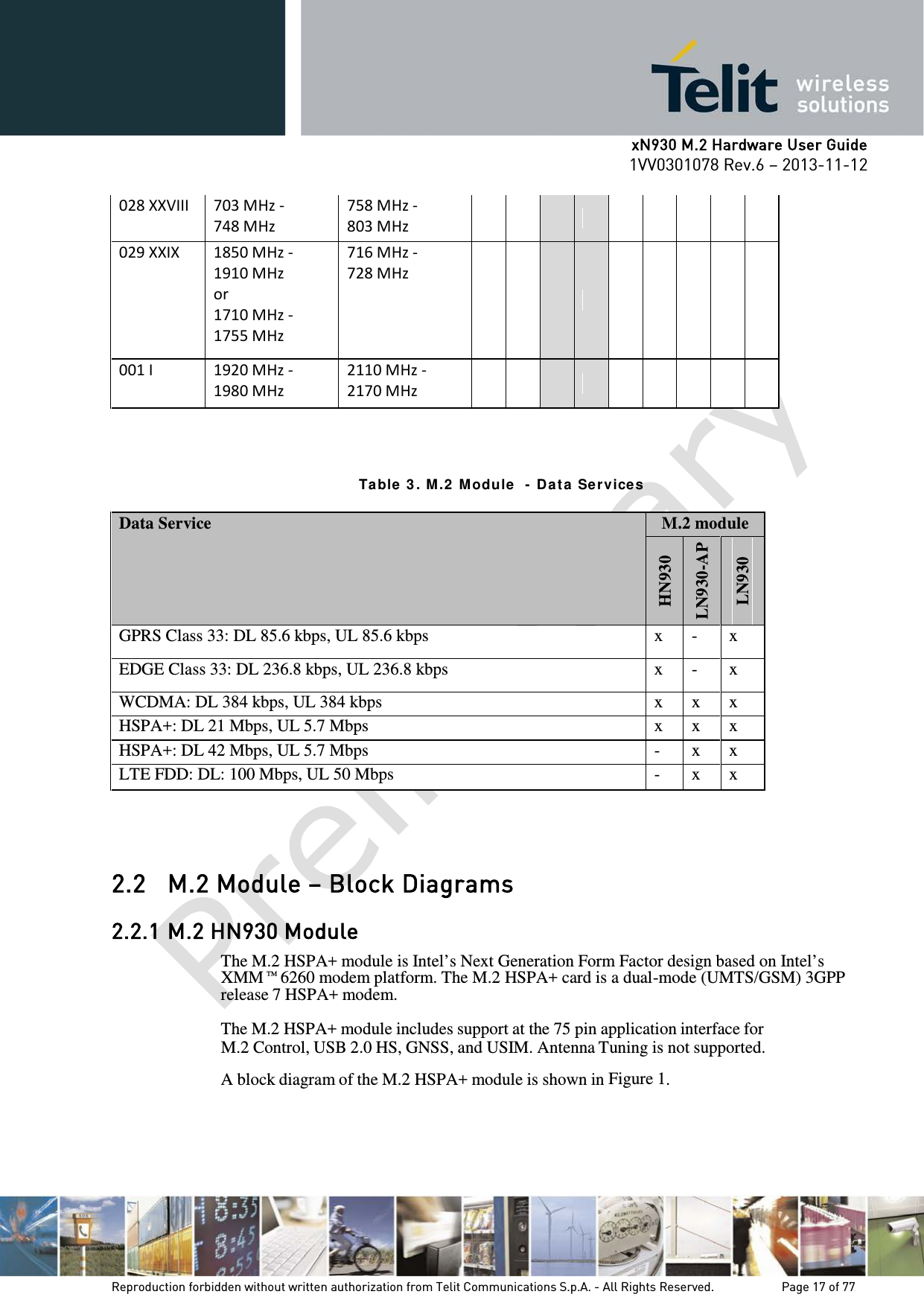
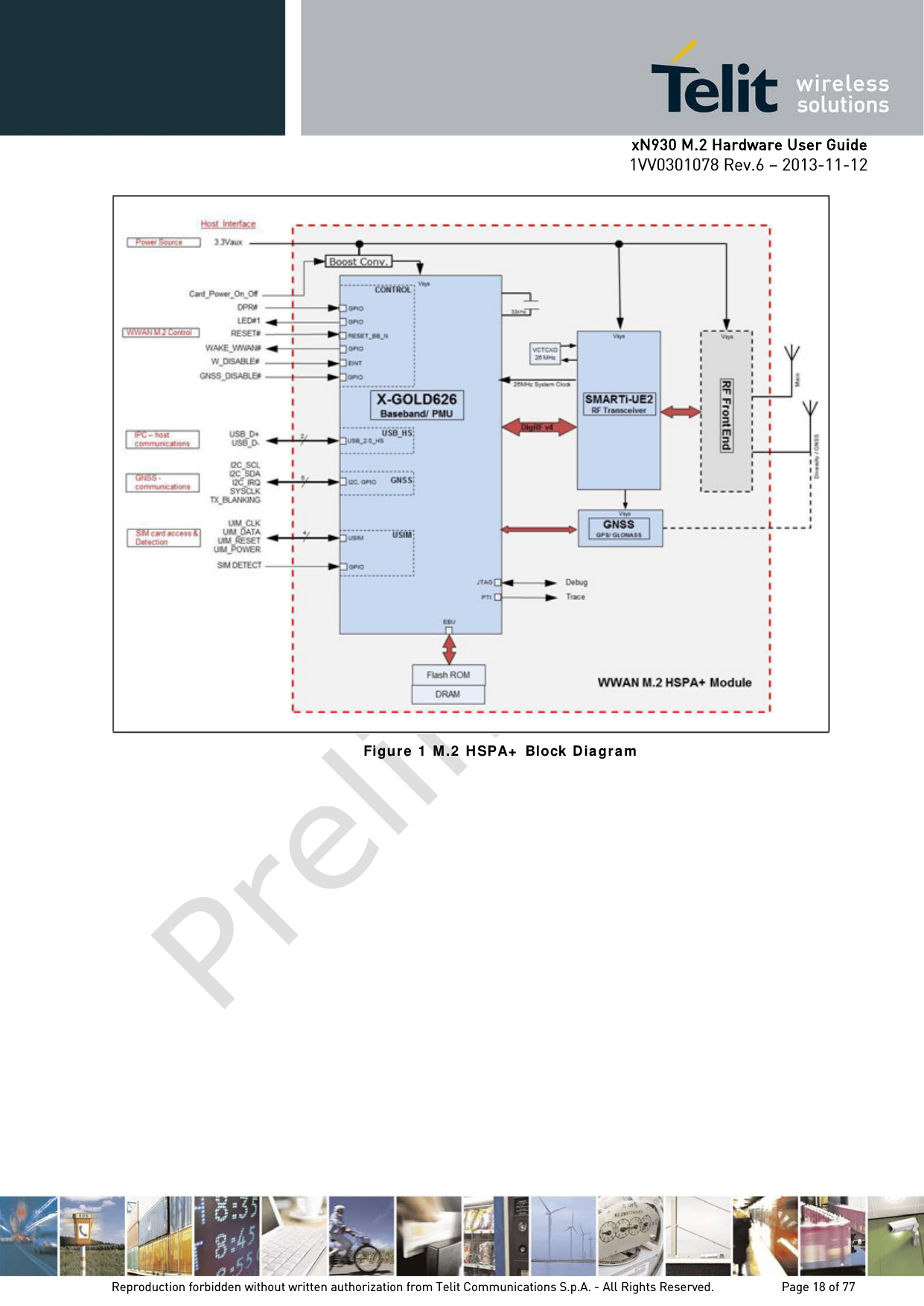
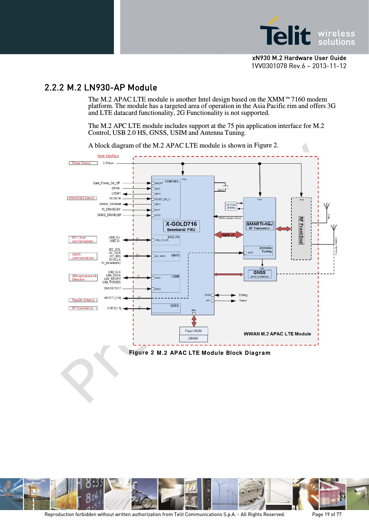
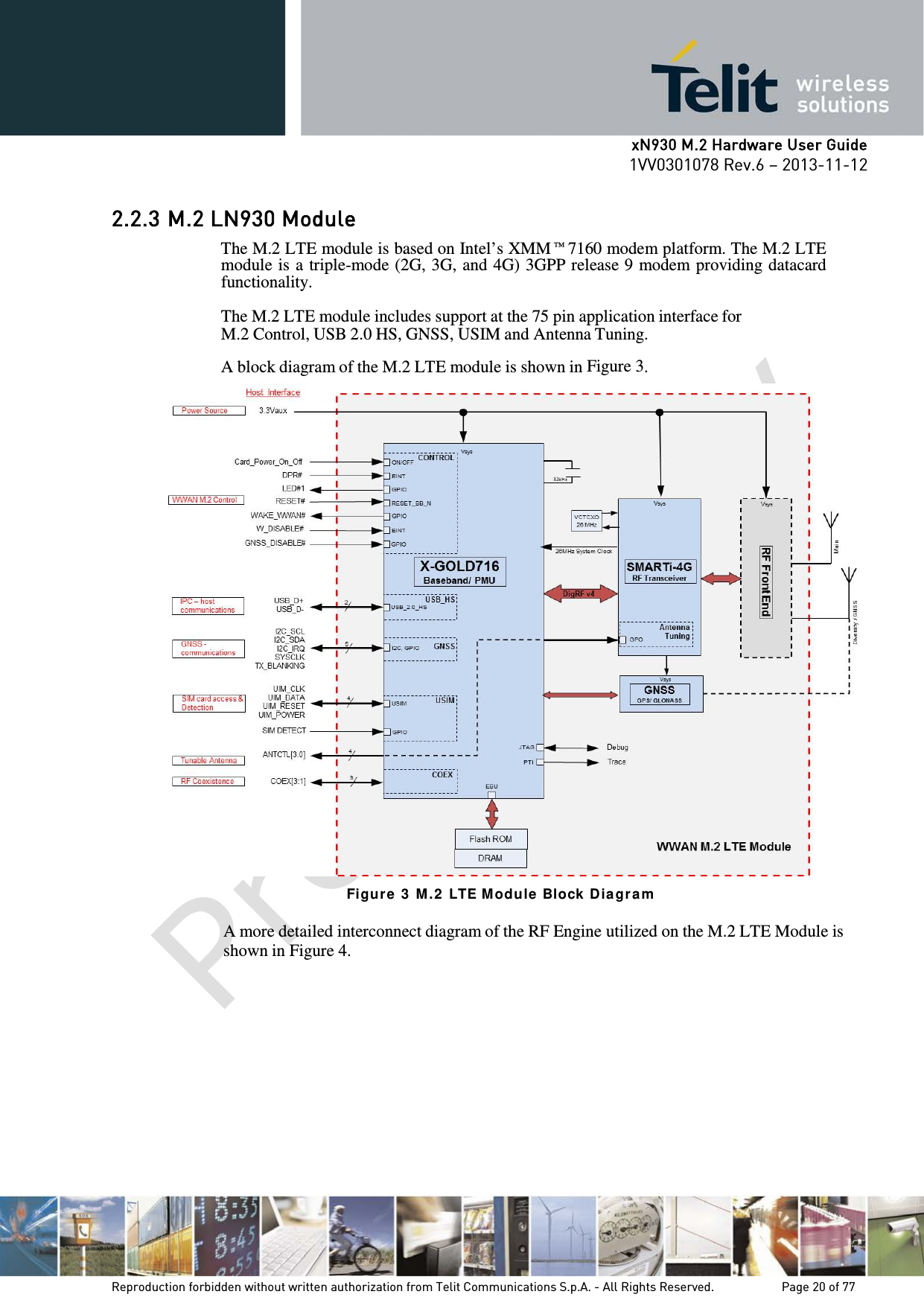
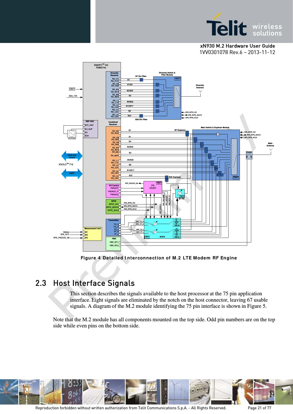
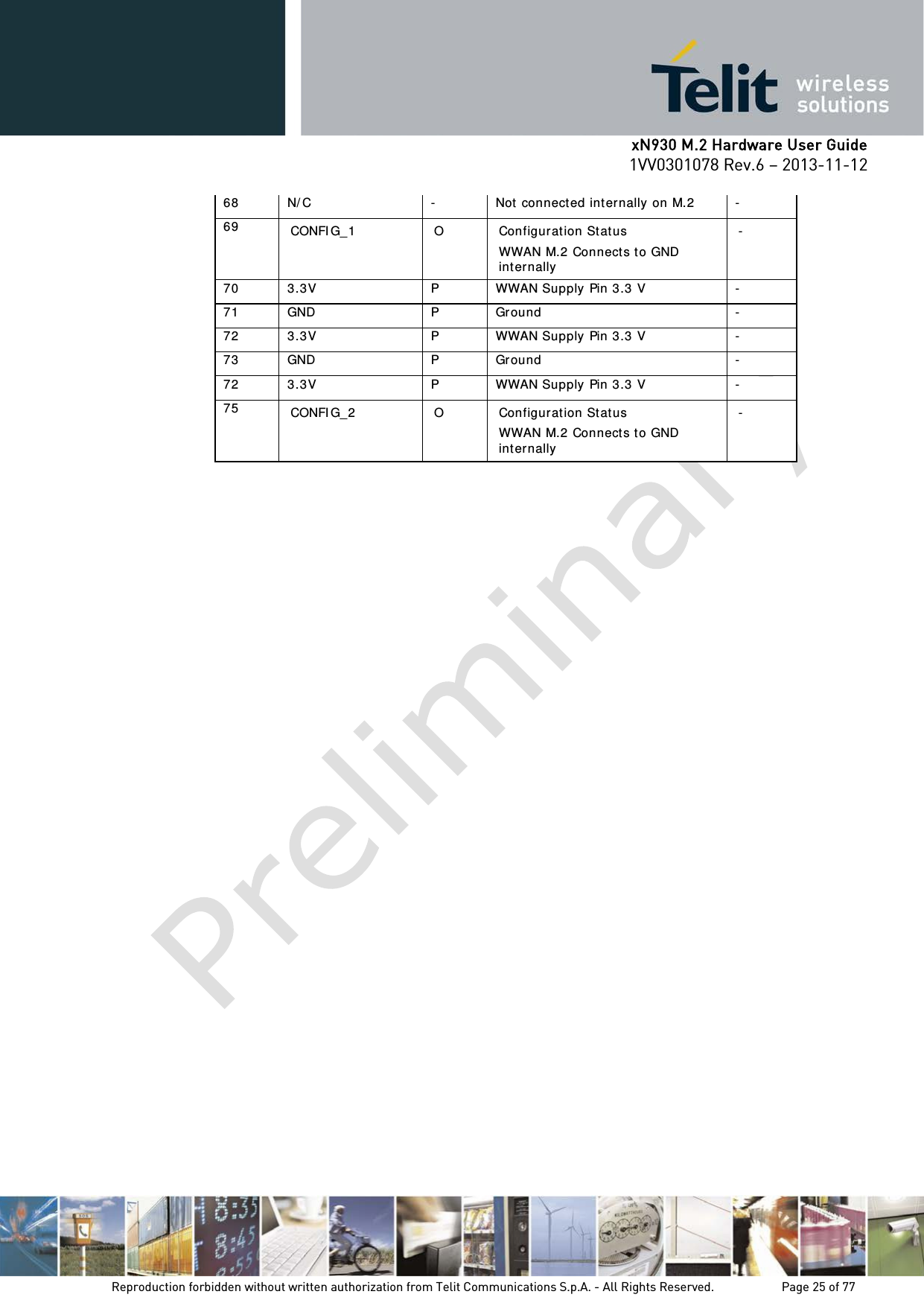
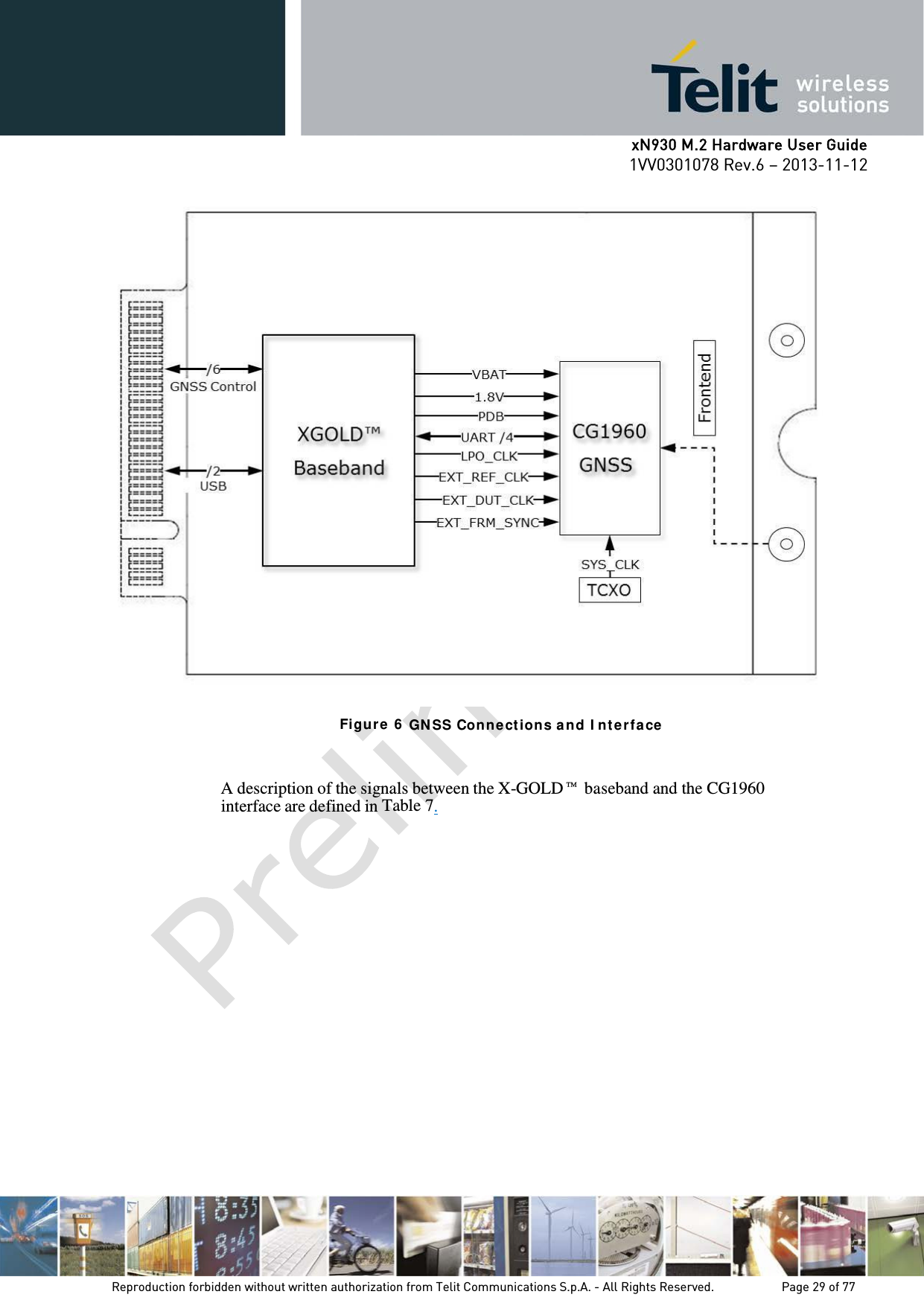
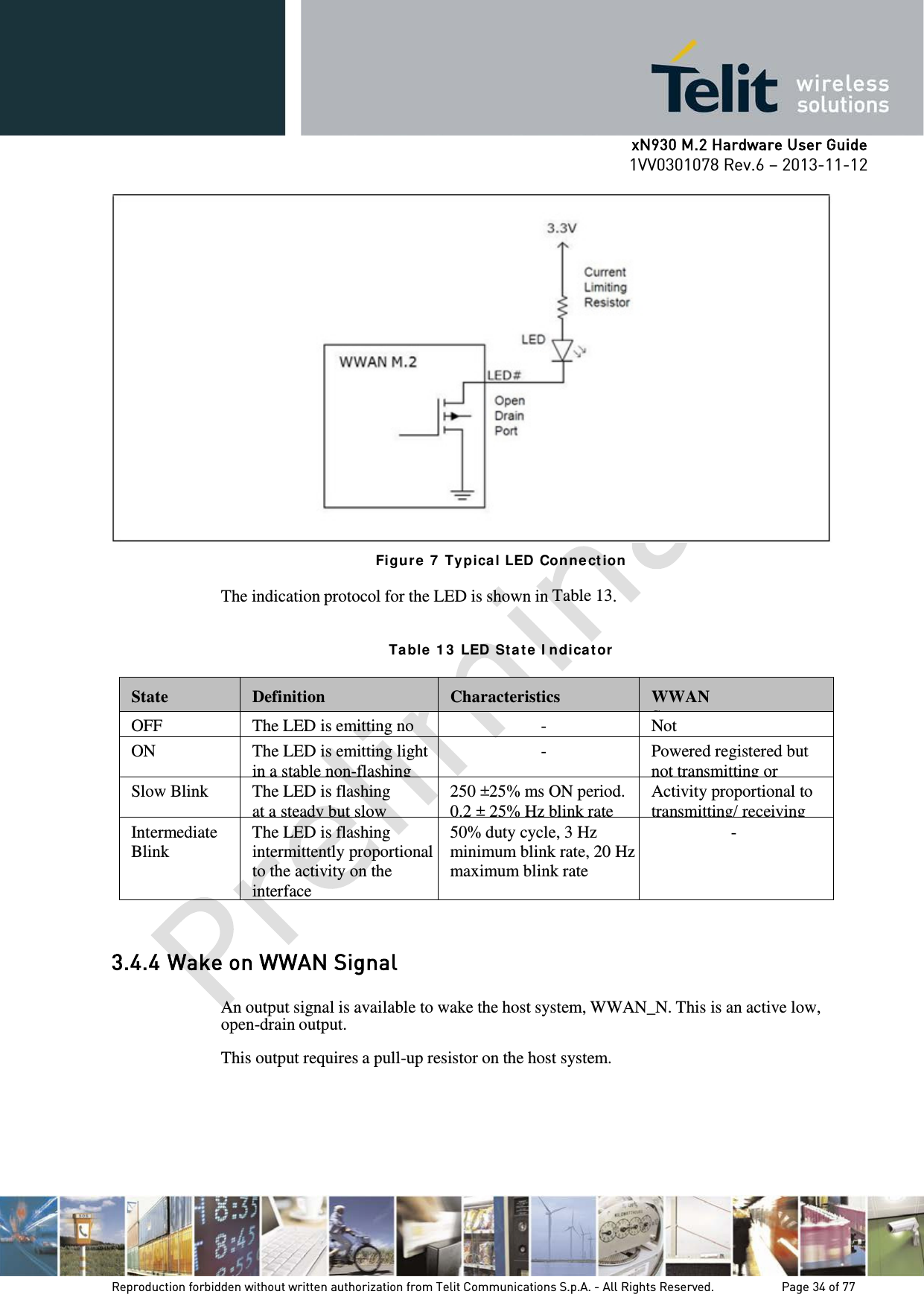
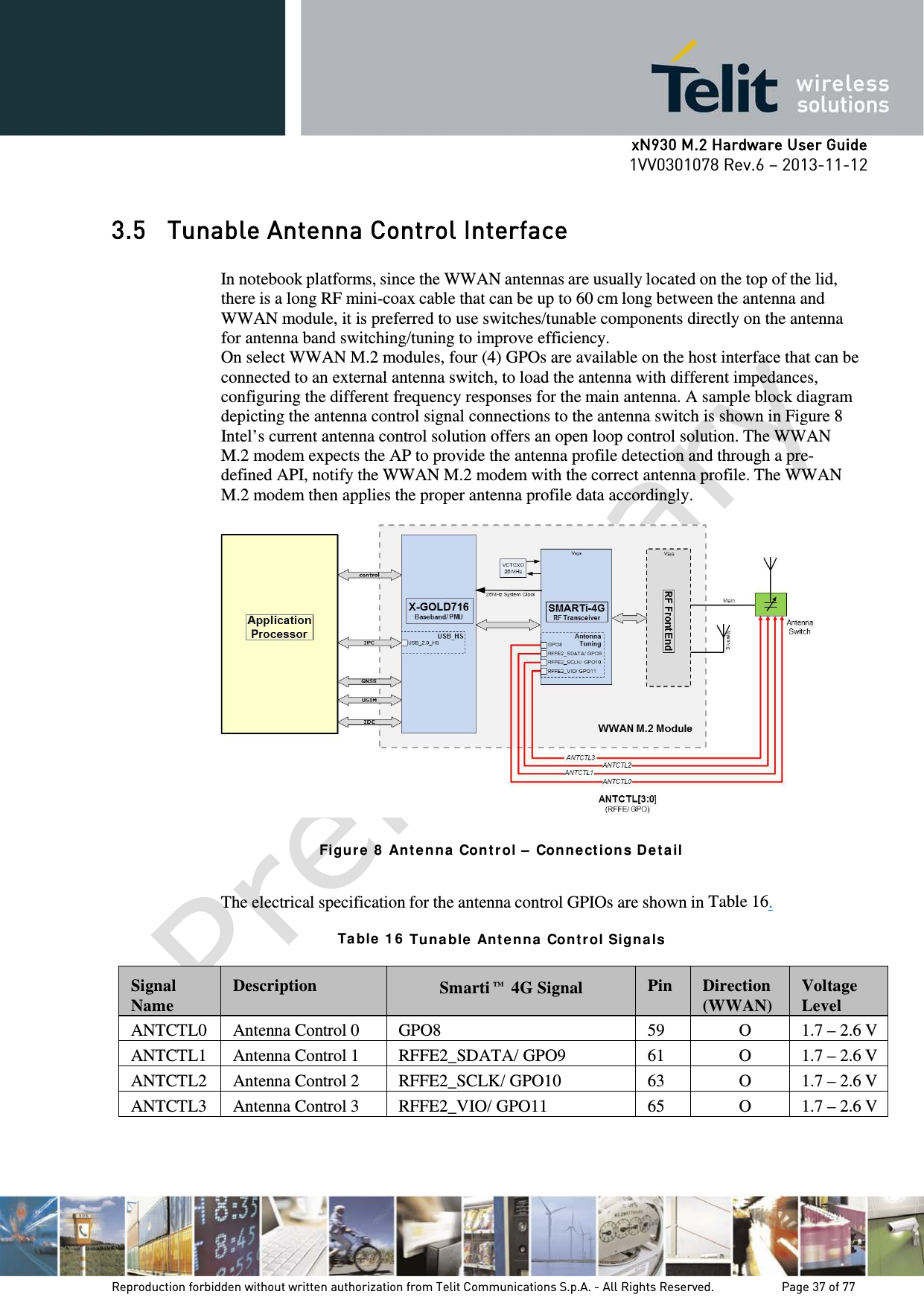
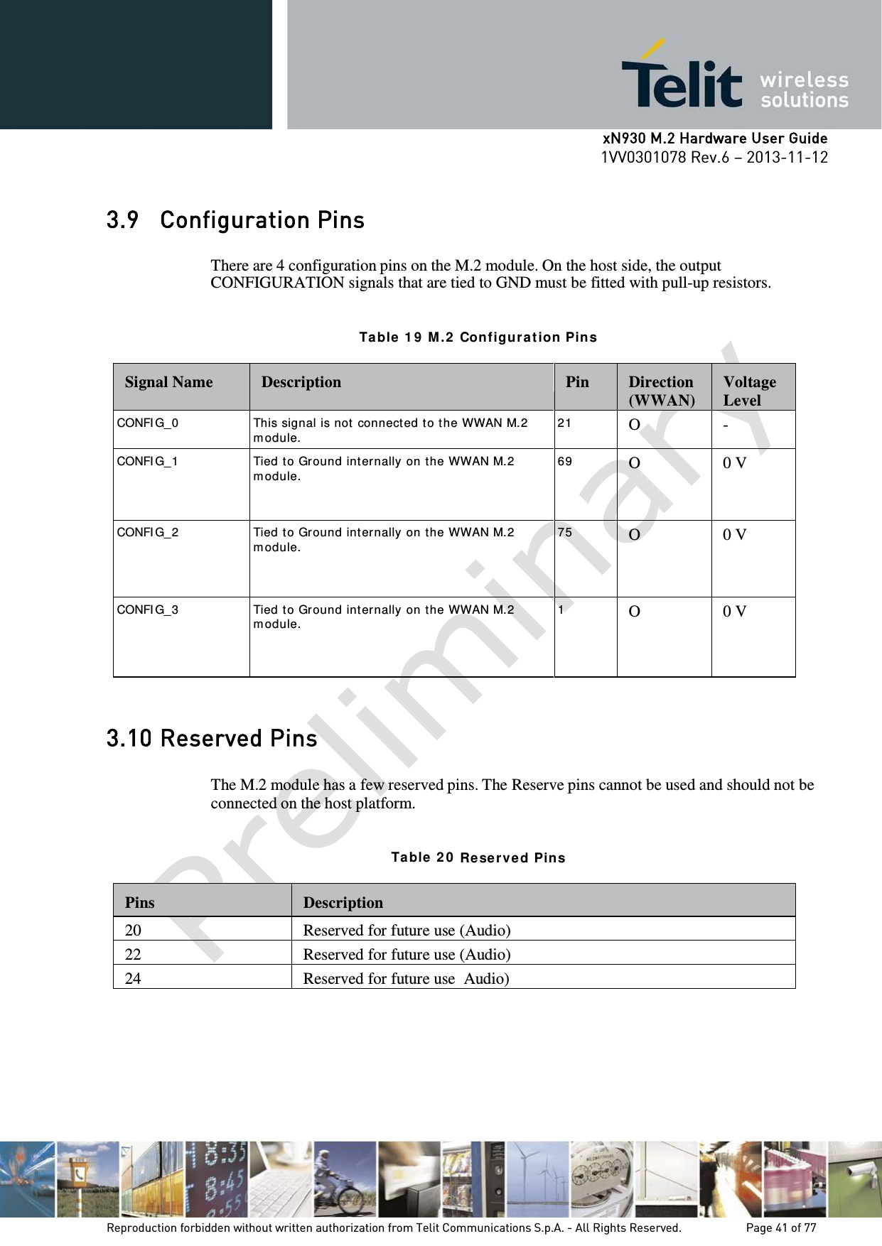
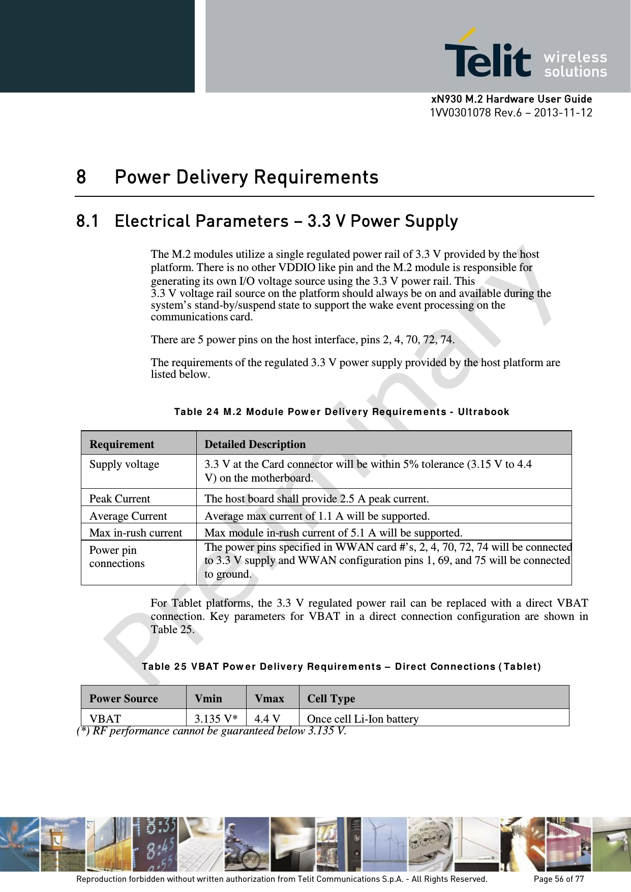
![xN930 M.2 Hardware User Guide 1VV0301078 Rev.6 – 2013-11-12 8.2 Electrical Parameters - Host Interface Signals Ta ble 2 6 Ele ct rica l Param e t ers – H ost I nterface Sign a ls Signal Pin Description I/O Voltage Domain (V) DC Characteristics (V) Min Typ Max (VDD_IO) Car d_Power_ON_OFF 6 Power On/ Off M.2 Module I 1.8 - 0.3 0/ 1.8 2.3 RESET# 67 Reset M.2 Module I 1.8 - 0.3 0/ 1.8 2.3 LED# 1 10 M.2 St at us I ndicator O (OD) 3 Open- Drain Out put , Host requ ir es pull-up resistor W_DI SABLE# 8 M.2 Disable I 1.8 - 0.3 1.8 2.1 WAKE_WWAN# 23 WWAN wak e Host O 1.8 -0.3 0/ 1.8 2.4 DPR# 25 Body SAR Det ect ion I 1.8 -0.3 0/ 1.8 2.1 USB ( D+ / D- ) 7, 9 USB D+ / D- 2.0 High-speed I / O 1.8/ 2.9 -0.3 1.8/ 2.9 VDDI O+ 0.3 SI M_DETECT 66 SI M Card Det ection I 1.8/ 2.9 -0.3 1.8/ 2.9 VDDI O+ 0.3 UI M_CLK 32 SI M Card Clock O 1.8/ 2.9 - 0.3 1.8/ 2.9 VDDI O+ 0.3 UI M_RESET 30 SI M Card Reset O 1.8 / 2.9 -0.3 1.8/ 2.9 VDDI O+ 0.3 UI M_DATA 34 Sim Car d DATA I / O 1.8/ 2.9 - 0.3 1.8/ 2.9 VDDI O+ 0.3 UI M_PWR 36 SI M Card Power O 1.8/ 2.9 - 0.3 1.8/ 2.9 VDDI O+ 0.3 I 2C_SCL 40 GNSS – I 2C Clock I / O 1.8 - 0.3 0/ 1.8 2.1 I 2C_SDA 42 GNSS – I 2C Dat a I / O 1.8 -0.3 0/ 1.8 2.1 I 2C_I RQ 44 GNSS – I 2C I nterr upt I 1.8 -0.3 0/ 1.8 2.1 CLKOUT0 46 GNSS – 26 MHz Clock Synch r onizat ion O 1.8 - 0.3 0/ 1.8 2.1 TX_BLANKI NG 48 GNSS – TX Blanking O 1.8 - 0.3 0/ 1.8 2.1 GNSS_DI SABLE# 26 Disable GNSS I 1.8 -0.3 0/ 1.8 2.1 ANTCTL[ 3: 0] 59, 61, 63, 65 Antenna Tuning Signals – RF Engine O 2.3 - 0.3 2.3 3.3 COEX[ 3: 1] 60, 62, 64 RF Coexist ence Synch r onizat ion I / O 1.8 -0.3 0/ 1.8 2.1 Reproduction forbidden without written authorization from Telit Communications S.p.A. - All Rights Reserved. Page 57 of 77](https://usermanual.wiki/Telit-Communications-S-p-A/LN930/User-Guide-2125568-Page-57.png)