Telit Communications S p A LN930 DATA CARD User Manual xN930 M 2 Hardware User Guide
Telit Communications S.p.A. DATA CARD xN930 M 2 Hardware User Guide
User Manual

xN930 M.2 Hardware User Guide
1VV0301078 Rev.6 – 2013-11-12

xN930 M.2 Hardware User Guide
1VV0301078 Rev.6 – 2013-11-12
SPECIFICATIONS SUBJECT TO CHANGE WITHOUT NOTICE
Notice
While reasonable efforts have been made to assure the accuracy of this document, Telit
assumes no liability resulting from any inaccuracies or omissions in this document, or from
use of the information obtained herein. The information in this document has been carefully
checked and is believed to be entirely reliable. However, no responsibility is assumed for
inaccuracies or omissions. Telit reserves the right to make changes to any products described
herein and reserves the right to revise this document and to make changes from time to time
in content hereof with no obligation to notify any person of revisions or changes. Telit does
not assume any liability arising out of the application or use of any product, software, or
circuit described herein; neither does it convey license under its patent rights or the rights of
others.
It is possible that this publication may contain references to, or information about Telit
products (machines and programs), programming, or services that are not announced in your
country. Such references or information must not be construed to mean that Telit intends to
announce such Telit products, programming, or services in your country.
Copyrights
This instruction manual and the Telit products described in this instruction manual may be,
include or describe copyrighted Telit material, such as computer programs stored in
semiconductor memories or other media. Laws in the Italy and other countries preserve for
Telit and its licensors certain exclusive rights for copyrighted material, including the
exclusive right to copy, reproduce in any form, distribute and make derivative works of the
copyrighted material. Accordingly, any copyrighted material of Telit and its licensors
contained herein or in the Telit products described in this instruction manual may not be
copied, reproduced, distributed, merged or modified in any manner without the express
written permission of Telit. Furthermore, the purchase of Telit products shall not be deemed
to grant either directly or by implication, estoppel, or otherwise, any license under the
copyrights, patents or patent applications of Telit, as arises by operation of law in the sale of a
product.
Computer Software Copyrights
The Telit and 3rd Party supplied Software (SW) products described in this instruction manual
may include copyrighted Telit and other 3rd Party supplied computer programs stored in
semiconductor memories or other media. Laws in the Italy and other countries preserve for
Telit and other 3rd Party supplied SW certain exclusive rights for copyrighted computer
programs, including the exclusive right to copy or reproduce in any form the copyrighted
computer program. Accordingly, any copyrighted Telit or other 3rd Party supplied SW
computer programs contained in the Telit products described in this instruction manual may
not be copied (reverse engineered) or reproduced in any manner without the express written
permission of Telit or the 3rd Party SW supplier. Furthermore, the purchase of Telit products
shall not be deemed to grant either directly or by implication, estoppel, or otherwise, any
license under the copyrights, patents or patent applications of Telit or other 3rd Party supplied
SW, except for the normal non-exclusive, royalty free license to use that arises by operation
of law in the sale of a product.
Reproduction forbidden without written authorization from Telit Communications S.p.A. - All Rights Reserved. Page 3 of 77

xN930 M.2 Hardware User Guide
1VV0301078 Rev.6 – 2013-11-12
Usage and Disclosure Restrictions
License Agreements
The software described in this document is the property of Telit and its licensors. It is
furnished by express license agreement only and may be used only in accordance with the
terms of such an agreement.
Copyrighted Materials
Software and documentation are copyrighted materials. Making unauthorized copies is
prohibited by law. No part of the software or documentation may be reproduced, transmitted,
transcribed, stored in a retrieval system, or translated into any language or computer language,
in any form or by any means, without prior written permission of Telit
High Risk Materials
Components, units, or third-party products used in the product described herein are NOT
fault-tolerant and are NOT designed, manufactured, or intended for use as on-line control
equipment in the following hazardous environments requiring fail-safe controls: the operation
of Nuclear Facilities, Aircraft Navigation or Aircraft Communication Systems, Air Traffic
Control, Life Support, or Weapons Systems (High Risk Activities"). Telit and its supplier(s)
specifically disclaim any expressed or implied warranty of fitness for such High Risk
Activities.
Trademarks
TELIT and the Stylized T Logo are registered in Trademark Office. All other product or
service names are the property of their respective owners.
Copyright © Telit Communications S.p.A. 2011.
Reproduction forbidden without written authorization from Telit Communications S.p.A. - All Rights Reserved. Page 4 of 77

xN930 M.2 Hardware User Guide
1VV0301078 Rev.6 – 2013-11-12
Contents
1 Introduction ......................................................................................................... 10
1.1 Scope .......................................................................................................................... 10
1.2 Purpose ...................................................................................................................... 10
1.3 Audience ..................................................................................................................... 10
1.4 Contact Information, Support .................................................................................... 10
1.5 Document Organization ............................................................................................. 11
1.6 Text Conventions ........................................................................................................ 11
1.7 Related Documents ................................................................................................... 11
2 M.2 Overview ........................................................................................................ 13
2.1 SKUs - 2G/3G/LTE M.2 Modules ................................................................................ 13
2.2 M.2 Module – Block Diagrams ................................................................................... 17
2.2.1 M.2 HN930 Module ......................................................................................................... 17
2.2.2 M.2 LN930-AP Module ................................................................................................... 19
2.2.3 M.2 LN930 Module ......................................................................................................... 20
2.3 Host Interface Signals ............................................................................................... 21
3 M.2 Module Interface Details ............................................................................... 26
3.1 USB 2.0 High-Speed – IPC Interface ......................................................................... 26
3.2 (U)SIM Interface ......................................................................................................... 27
3.3 GNSS Interface ........................................................................................................... 27
3.4 System Control Interface ........................................................................................... 30
3.4.1 Power On & Reset .......................................................................................................... 31
3.4.2 Host Radio Disable Operation ........................................................................................ 31
3.4.3 LED Interface – Status Indicator .................................................................................... 33
3.4.4 Wake on WWAN Signal ................................................................................................... 34
3.4.5 Dynamic Power Reduction ............................................................................................. 35
3.5 Tunable Antenna Control Interface ........................................................................... 37
3.6 In-Device Coexistence Interface ................................................................................ 38
3.7 Power Supply Interface .............................................................................................. 40
3.8 Trace & Debug Interface ............................................................................................ 40
Reproduction forbidden without written authorization from Telit Communications S.p.A. - All Rights Reserved. Page 5 of 77

xN930 M.2 Hardware User Guide
1VV0301078 Rev.6 – 2013-11-12
3.9 Configuration Pins ..................................................................................................... 41
3.10 Reserved Pins ............................................................................................................ 41
3.11 No Connect Pins ......................................................................................................... 42
3.12 Antenna Interface ...................................................................................................... 42
4 Development Tools ............................................................................................... 44
4.1 Carrier Board ............................................................................................................. 44
4.1.1 FlashTool........................................................................................................................ 45
4.1.2 PhoneTool ...................................................................................................................... 45
4.1.3 System Trace Tool .......................................................................................................... 46
4.1.4 RF Calibration ................................................................................................................ 46
4.1.5 Noise Profiling Scan Tool ............................................................................................... 47
4.1.6 GNSS Tools .................................................................................................................... 48
5 Windows Software Components ........................................................................... 49
5.1 MBIM Toolkit .............................................................................................................. 50
5.1.1 Windows® 7 MBIM driver .............................................................................................. 50
5.1.2 GNSS UMDF driver for Windows® 7 and Windows® 8 ................................................. 50
5.1.3 M.2 module Firmware Update ....................................................................................... 50
5.1.4 End User Trace Tool....................................................................................................... 50
6 Modem Configuration on Linux Based PC ............................................................. 51
6.1 Overview ..................................................................................................................... 51
6.2 CMUX Multiplexer ...................................................................................................... 52
6.3 USB 2.0 HS Features .................................................................................................. 53
6.4 USB Configuration ..................................................................................................... 53
6.4.1 Modem Connection ........................................................................................................ 53
6.4.2 Network Connection ...................................................................................................... 53
6.4.3 Default Configuration ..................................................................................................... 54
6.5 LPM ............................................................................................................................ 54
6.5.1 Suspend/Resume and Remote Wake-up ....................................................................... 54
7 Operating Environment ........................................................................................ 55
8 Power Delivery Requirements .............................................................................. 56
8.1 Electrical Parameters – 3.3 V Power Supply ............................................................. 56
Reproduction forbidden without written authorization from Telit Communications S.p.A. - All Rights Reserved. Page 6 of 77

xN930 M.2 Hardware User Guide
1VV0301078 Rev.6 – 2013-11-12
8.2 Electrical Parameters - Host Interface Signals ........................................................ 57
8.3 Power Consumption ................................................................................................... 58
9 Other Information ................................................................................................ 60
9.1 EMI/EMC and Platform Noise .................................................................................... 60
9.2 Platform Noise Mitigation - Adaptive Clocking ......................................................... 60
9.3 Thermal Monitoring ................................................................................................... 60
9.4 Seamless Roaming / Wifi Offload .............................................................................. 61
9.5 Conducted Transmit Power ....................................................................................... 61
9.6 Conducted Receiver Sensitivity .................................................................................. 61
9.7 Antenna Recommendations ...................................................................................... 62
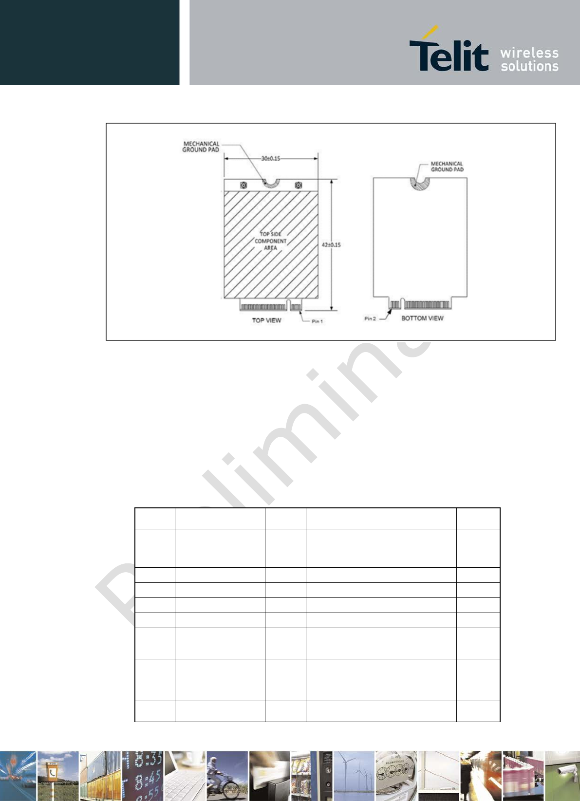
10 WWAN Card Type 3042-S3-B ............................................................................. 64
10.1 Mechanical Dimensions ............................................................................................. 64
10.2 Land Pattern .............................................................................................................. 66
10.3 Antenna Connector Locations ................................................................................... 68
11 Safety Recommendations .................................................................................. 69
12 Conformity assessment issues.......................................................................... 70
12.1 1999/5/EC Directive ................................................................................................... 70
12.2 CE RF Exposure Compliance ..................................................................................... 72
12.3 R&TTE Regulation:..................................................................................................... 73
13 FCC/IC Regulatory notices ................................................................................ 74
13.1 Modification statement .............................................................................................. 74
13.2 Interference statement .............................................................................................. 74
13.3 FCC Class B digital device notice .............................................................................. 74
13.4 Radiation Exposure Statement .................................................................................. 75
13.5 End Product Labeling ................................................................................................ 75
14 Document History ............................................................................................. 76
Reproduction forbidden without written authorization from Telit Communications S.p.A. - All Rights Reserved. Page 7 of 77

xN930 M.2 Hardware User Guide
1VV0301078 Rev.6 – 2013-11-12
Figure 1 M.2 HSPA+ Block Diagram ................................................................................................................ 18
Figure 3 M.2 LTE Module Block Diagram........................................................................................................ 19
Figure 4 M.2 LTE Module Block Diagram........................................................................................................ 20
Figure 5 Detailed Interconnection of M.2 LTE Modem RF Engine .................................................................. 21
Figure 6 PCI Express M.2 Module Interface ..................................................................................................... 22
Figure 7 GNSS Connections and Interface ........................................................................................................ 29
Figure 8 Typical LED Connection ..................................................................................................................... 34
Figure 9 Antenna Control – Connections Detail ................................................................................................ 37
Figure 10 In-Device Coexistence Architecture .................................................................................................. 38
Figure 11 RF Antenna – Coaxial Connector Location ....................................................................................... 43
Figure 12 M.2 Carrier Board .............................................................................................................................. 45
Figure 13 Windows Software Architecture ........................................................................................................ 49
Figure 14 Linux Software Architecture ............................................................................................................. 51
Figure 15 WWAN Card 3042 Top/Bottom-View .............................................................................................. 64
Figure 16 WWAN Card 3042 Edge-View ......................................................................................................... 65
Figure 17 WWAN Card Type 3042 Top-Side Mounting Land Pattern with Key Removed ............................. 66
Figure 18 WWAN Card 3042 Mid-plane Land Pattern with Key Removed ..................................................... 67
Figure 19 Antenna Connector Location ............................................................................................................. 68
Reproduction forbidden without written authorization from Telit Communications S.p.A. - All Rights Reserved. Page 8 of 77

xN930 M.2 Hardware User Guide
1VV0301078 Rev.6 – 2013-11-12
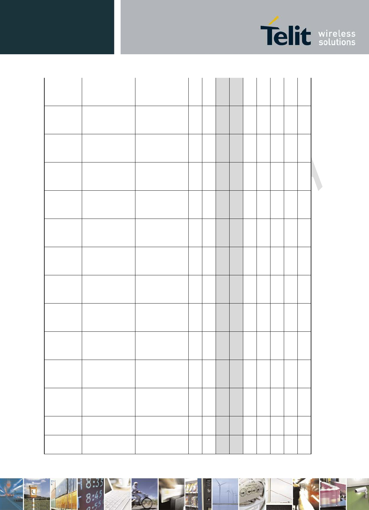
Table 1 M.2 Module - General Feature .............................................................................................................. 14
Table 2. M.2 Module - RF Band Support ......................................................................................................... 15
Table 3. M.2 Module - Data Services ............................................................................................................... 17
Table 4 M.2 Host Interface Signals .................................................................................................................... 22
Table 5 USB HS Interprocessor Communications In
ter
face .............................................................................. 26
Table 6 (U)SIM Interface Signals ...................................................................................................................... 27
Table 7 X-GOLD™ Baseband to GNSS Interface Signals ................................................................................ 30
Table 8 GNSS Module Interface Signals ........................................................................................................... 30
Table 9 Power-on & Reset Signals .................................................................................................................... 31
Table 10 Radio Disable Signal........................................................................................................................... 32
Table 11 Host Radio Disable Interface (W_DISABLE#) .................................................................................. 33
Table 12 LED#1 Signal...................................................................................................................................... 33
Table 13 LED State Indicator ............................................................................................................................ 34
Table 14 Wake on WWAN Signal ..................................................................................................................... 35
Table 15 DPR#/ SAR Support Signal ................................................................................................................ 36
Table 16 Tunable Antenna Control Signals ....................................................................................................... 37
Table 17 Coexistence – Hardware Synchronization Signals .............................................................................. 39
Table 18 Power & Ground Signals .................................................................................................................... 40
Table 19 M.2 Configuration Pins ....................................................................................................................... 41
Table 20 Reserved Pins ...................................................................................................................................... 41
Table 21 No Connect Pins ................................................................................................................................. 42
Table 22 Antenna Requirements ........................................................................................................................ 42
Table 23 Operating Environment ....................................................................................................................... 55
Table 24 M.2 Module Power Delivery Requirements - Ultrabook .................................................................... 56
Table 25 VBAT Power Delivery Requirements – Direct Connections (Tablet) ................................................ 56
Table 26 Electrical Parameters – Host Interface Signals ................................................................................... 57
Table 27 LTE Power Consumption .................................................................................................................... 58
Table 28 UMTS Power Consumption ................................................................................................................ 58
Table 29 GSM Power Consumption .................................................................................................................. 58
Table 30 Conducted Transmit Power ................................................................................................................. 61
Table 31 Antenna Recommendation .................................................................................................................. 62
Table 32 Antenna Recommendation - Bandwidth of Main & Diversity Antenna ............................................. 62
Reproduction forbidden without written authorization from Telit Communications S.p.A. - All Rights Reserved. Page 9 of 77

xN930 M.2 Hardware User Guide
1VV0301078 Rev.6 – 2013-11-12
1 Introduction
This document is a technical specification for Telit’s next generation form factor M.2 module
family. The next generation form factor M.2 module family is a natural transition from the
PCI Express Mini Card and Half Mini Card to a smaller form factor size.
The M.2 Card Type 3042 offers single sided component mounting, 75 pins (8 dedicated for
key), in a compact size (30 mm x 42 mm). A range of 2G/3G/4G (LTE) M.2 modules
supporting multiple operating systems and unique features in the WWAN Card Type 3042
form factor are available.
1.1 Scope
The document will cover the features of the M.2 modules presently available. It will also
identify the M.2 module application interface along with hardware, software, reliability, and
mechanical specifications.
1.2 Purpose
The intent of this document is to provide design guidelines and information for each M.2
module.
In addition to the M.2 module family features and performance metrics, this document
describes the interface signals, operating conditions, physical and mechanical requirements of
the M.2 cards.
1.3 Audience
This document is intended for editors who are about to write or edit documentation for Telit.
1.4 Contact Information, Support
For general contact, technical support, to report documentation errors and to order manuals,
contact Telit Technical Support Center (TTSC) at:
TS-EMEA@telit.com
TS-NORTHAMERICA@telit.com
TS-LATINAMERICA@telit.com
TS-APAC@telit.com
Alternatively, use:
http://www.telit.com/en/products/technical-support-center/contact.php
For detailed information about where you can buy the Telit modules or for recommendations
on accessories and components visit:
Reproduction forbidden without written authorization from Telit Communications S.p.A. - All Rights Reserved. Page 10 of 77
xN930 M.2 Hardware User Guide
1VV0301078 Rev.6 – 2013-11-12
http://www.telit.com
To register for product news and announcements or for product questions contact Telit
Technical Support Center (TTSC).
Our aim is to make this guide as helpful as possible. Keep us informed of your comments and
suggestions for improvements.
Telit appreciates feedback from the users of our information.
1.5 Document Organization
This document contains the following chapters (sample):
“Chapter 1: “Introduction” provides a scope for this document, target audience, contact and
support information, and text conventions.
“Chapter 2: “Chapter two” gives an overview of the features of the product.
“Chapter 3: “Chapter three” describes in details the characteristics of the product.
“Chapter 6: “Conformity Assessment Issues” provides some fundamental hints about the
conformity assessment that the final application might need.
“Chapter 7: “Safety Recommendation” provides some safety recommendations that must be
follow by the customer in the design of the application that makes use of the AA99-XXX.
1.6 Text Conventions
Danger – This information MUST be followed or catastrophic equipment failure or bodily
injury may occur.
Caution or Warning – Alerts the user to important points about integrating the module, if
these points are not followed, the module and end user equipment may fail or malfunction.
Tip or Information – Provides advice and suggestions that may be useful when
integrating the module.
All dates are in ISO 8601 format, i.e. YYYY-MM-DD.
1.7 Related Documents
• TBA
Reproduction forbidden without written authorization from Telit Communications S.p.A. - All Rights Reserved. Page 11 of 77


xN930 M.2 Hardware User Guide
1VV0301078 Rev.6 – 2013-11-12
2 M.2 Overview
This section will provide an overview of the standard features of a M.2 Card, information on
the various SKUs of 2G/3G/4G (LTE) M.2 modules along with a respective functional block
diagram of each SKU.
2.1 SKUs - 2G/3G/LTE M.2 Modules
There are five different M.2 modules available in the M.2 Card Type 3042 form factor:
• HN930 - HSPA+
• LN930-AP - APAC LTE
• LN930 - LTE
A comparison of the features, RF band Support, and data rates for the various M.2 modules is
shown in Table 1 through Table 3
Reproduction forbidden without written authorization from Telit Communications S.p.A. - All Rights Reserved. Page 13 of 77
xN930 M.2 Hardware User Guide
1VV0301078 Rev.6 – 2013-11-12
Ta ble 1 M .2 Module - Ge ne r a l Feat ure
Feature
Description
Additional Information
M.2 module
HN930
LN930-AP
LN930
Mechanical
M.2 Card Type 3042
Slot B
30 mm x 42 mm
Pin count: 75
(67 usable, 8 slot) x x x
Operating
Voltage
3.3 V Typical
-
x x x
Operating
Temperature
-10˚C to +55˚C – Normal
+55˚C to +70˚C –
Extended
E
xtreme - This is the
surrounding air temperature of
the module inside the platform
when the card is fully operating
at worst case condition
x x x
Application
Interface
(75 pin card)
USB 2.0 High-speed
Interprocessor
Communications x x x
USIM w/ Card Detect
SIM_CLK, SIM_RESET,
SIM_IO, SIM_PWR,
SIM_DETECT
x x x
M.2 Control
Full_Card_Power_On_Off
x x x
Reset#
x
x
x
W_DISABLE#
x x x
LED #1
x
x
x
DPR (Body SAR)
x x x
Wake on WWAN
x
x
x
GNSS Disable
x x x
Global Positioning
(GPS/ GLONASS)
I2C_SCL, I2C_SDA, I2_IRQ,
CLKOUT, TX_BLANKING x x x
Antenna Tuning
(4) GPO (RF Transceiver)
- x x
RF Coexistence
(3) GPIO
-
x
x
RF Antenna
Main & Diversity/ GNSS
Separate coax connectors
x x x
Debug
JTAG
-
x
x
x
ETM11
-
-
x
x
MIPI PTI
-
- x X
Reproduction forbidden without written authorization from Telit Communications S.p.A. - All Rights Reserved. Page 14 of 77
xN930 M.2 Hardware User Guide
1VV0301078 Rev.6 – 2013-11-12
Ta ble 2. M .2 M odule - RF Ba n d Su p port
RF Band
UE Transmit
UE Receive
M.2 Module
HN930
LN930-AP
LN930
GSM
UMTS
LTE
GSM
UMTS
LTE
GSM
UMTS
LTE
001 I
1920 MHz -
1980 MHz
2110 MHz -
2170 MHz x x x x x
002 II
1850 MHz -
1910 MHz
1930 MHz -
1990 MHz x x x x x
003 III
1710 MHz -
1785 MHz
1805 MHz -
1880 MHz x x x x
004 IV
1710 MHz -
1755 MHz
2110 MHz -
2155 MHz x x x
005 V
824 MHz -
849 MHz
869 MHz -
894 MHz x x x x x
006 VI
830 MHz -
840 MHz
875 MHz -
885 MHz x
007 VII
2500 MHz -
2570 MHz
2620 MHz -
2690 MHz x
008 VIII
880 MHz -
915 MHz
925 MHz -
960 MHz x x x x x x x
009 IX
1749.9 MHz -
1784.9 MHz
1844.9 MHz -
1879.9 MHz x x
010 X
1710 MHz -
1770 MHz
2110 MHz -
2170 MHz
011 XI
1427.9 MHz -
1447.9 MHz
1475.9 MHz -
1495.9 MHz x x
Reproduction forbidden without written authorization from Telit Communications S.p.A. - All Rights Reserved. Page 15 of 77
xN930 M.2 Hardware User Guide
1VV0301078 Rev.6 – 2013-11-12
012 XII
699 MHz -
716 MHz
729 MHz -
746 MHz
013 XIII
777 MHz -
787 MHz
746 MHz -
756 MHz x
014 XIV
788 MHz -
798 MHz
758 MHz -
768 MHz
017 XVII
704 MHz -
716 MHz
7734 MHz -
746 MHz x
018 XVIII
815 MHz -830
MHz
860 MHz -875
MHz x x
019 XIX
830 MHz -
845 MHz
875 MHz -
890 MHz x x
020 XX
832 MHz -
862 MHz
791 MHz -
821 MHz x
021 XXI
1447.9 MHz -
1462.9 MHz
1495.9 MHz -
1510.9 MHz x
022 XXII
3410 MHz -
3490 MHz
3510 MHz -
3590 MHz
023 XXIII
2000 MHz -
2020 MHz
2180 MHz -
2200 MHz
024 XXIV
1626.5 MHz -
1660.5 MHz
1525 MHz -
1559 MHz
025 XXV
1850 MHz -
1915 MHz
1930 MHz -
1995 MHz
026 XXVI
814 MHz -
849 MHz
859 MHz -
894 MHz x
027 XXVII
806 MHz -
824 MHz
851 MHz -
869 MHz
Reproduction forbidden without written authorization from Telit Communications S.p.A. - All Rights Reserved. Page 16 of 77
xN930 M.2 Hardware User Guide
1VV0301078 Rev.6 – 2013-11-12
028 XXVIII
703 MHz -
748 MHz
758 MHz -
803 MHz
029 XXIX
1850 MHz -
1910 MHz
or
1710 MHz -
1755 MHz
716 MHz -
728 MHz
001 I
1920 MHz -
1980 MHz
2110 MHz -
2170 MHz
Ta ble 3. M .2 M odule - D a ta Se rvice s
Data Service
M.2 module
HN930
LN930-AP
LN930
GPRS Class 33: DL 85.6 kbps, UL 85.6 kbps
x
-
x
EDGE Class 33: DL 236.8 kbps, UL 236.8 kbps
x
-
x
WCDMA: DL 384 kbps, UL 384 kbps
x
x
x
HSPA+: DL 21 Mbps, UL 5.7 Mbps
x
x
x
HSPA+: DL 42 Mbps, UL 5.7 Mbps
-
x
x
LTE FDD: DL: 100 Mbps, UL 50 Mbps
-
x
x
2.2 M.2 Module – Block Diagrams
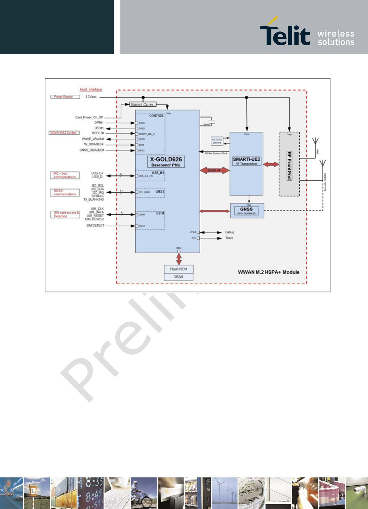
2.2.1 M.2 HN930 Module
The M.2 HSPA+ module is Intel’s Next Generation Form Factor design based on Intel’s
XMM™6260 modem platform. The M.2 HSPA+ card is a dual-mode (UMTS/GSM) 3GPP
release 7 HSPA+ modem.
The M.2 HSPA+ module includes support at the 75 pin application interface for
M.2 Control, USB 2.0 HS, GNSS, and USIM. Antenna Tuning is not supported.
A block diagram of the M.2 HSPA+ module is shown in Figure 1.
Reproduction forbidden without written authorization from Telit Communications S.p.A. - All Rights Reserved. Page 17 of 77
xN930 M.2 Hardware User Guide
1VV0301078 Rev.6 – 2013-11-12
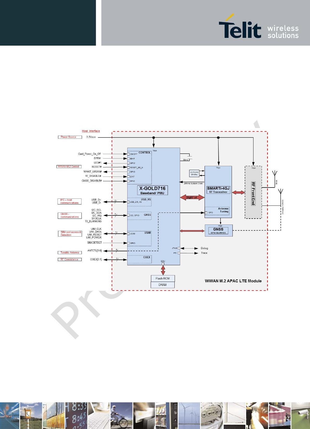
2.2.2 M.2 LN930-AP Module
The M.2 APAC LTE module is another Intel design based on the XMM™7160 modem
platform. The module has a targeted area of operation in the Asia Pacific rim and offers 3G
and LTE datacard functionality, 2G Functionality is not supported.
The M.2 APC LTE module includes support at the 75 pin application interface for M.2
Control, USB 2.0 HS, GNSS, USIM and Antenna Tuning.
A block diagram of the M.2 APAC LTE module is shown in Figure 2.
Figur e 2 M .2 APAC LTE M odu le Block Dia gr am
Reproduction forbidden without written authorization from Telit Communications S.p.A. - All Rights Reserved. Page 19 of 77
xN930 M.2 Hardware User Guide
1VV0301078 Rev.6 – 2013-11-12
2.2.3 M.2 LN930 Module
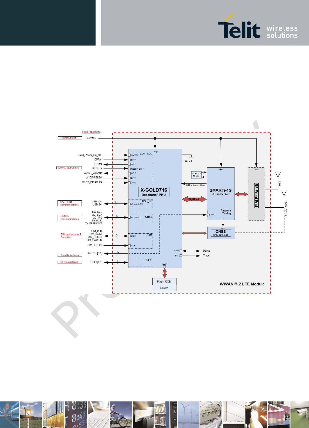
The M.2 LTE module is based on Intel’s XMM™7160 modem platform. The M.2 LTE
module is a triple-mode (2G, 3G, and 4G) 3GPP release 9 modem providing datacard
functionality.
The M.2 LTE module includes support at the 75 pin application interface for
M.2 Control, USB 2.0 HS, GNSS, USIM and Antenna Tuning.
A block diagram of the M.2 LTE module is shown in Figure 3.
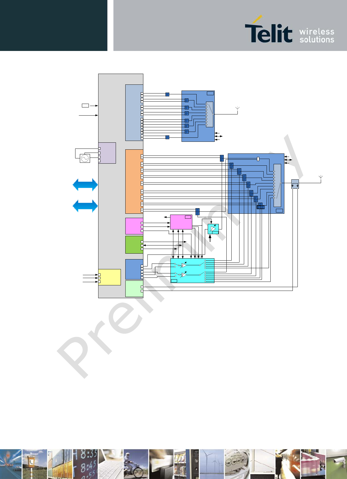
Figur e 3 M .2 LTE M odu le Block Dia gr a m
A more detailed interconnect diagram of the RF Engine utilized on the M.2 LTE Module is
shown in Figure 4.
Reproduction forbidden without written authorization from Telit Communications S.p.A. - All Rights Reserved. Page 20 of 77
xN930 M.2 Hardware User Guide
1VV0301078 Rev.6 – 2013-11-12
SMARTi
TM
4G
PMB5740
RD_H1
RD_H1X
RD_H3
RD_H3X
RD_M1
RD_M1X
RD_L1
RD_L1X
RD_L2
RD_L2X
RD_L4
RD_L4X
Clock and
Control
DigRF
VBAT
SD2_1V8
AFC_DAC
REF OSC
XO_SUP
XO
VCTCXO
Measurement Unit
M1
M2
M3
Battery
RFE_NTC
RFE_PADCDC_MI
XOX
Diversity
Receiver
Combined
Receiver
RX_H2
RX_H2X
RX_H3
RX_H3X
RX_H4
RX_H4X
RX_M1
RX_M1X
RX_M2
RX_M2X
RX_L1
RX_L1X
RX_L2
RX_L2X
RX_L4
RX_L4X
RFFE
RFFE_VIO
RFFE_SDATA
RFFE_SCLK
Transmitter
TQ_X
TQ_H
TQ_L
TP_H
TP_L
PA Control
PADACS
PADACF
PADACF_P
FBR
FBR_RF1
FBR_RF2
XGOLD
TM
716
B7
B1/B4
Diversity Switch &
Filter Module
Diversity
Antenna
RFE_RFFE_VIO
RFE_RFFE_SDATA
RFE_RFFE_SCLK
RFE_RFFE_VIO
RFE_RFFE_SCLK
RFE_RFFE_SDATA
Main Switch & Duplexer Module
B7 Duplexer
B7 Div Filter
B20 Div Filter
Coupler
Main
Antenna
RFE_RFFE_VIO
RFE_RFFE_SCLK
RFE_RFFE_SDATA
PA
DCDC
RFE_TQ_H
RFE_TP_H
RFE_TP_L
RFE_TQ_L
B2/B25
VBAT
VBAT
VBAT
RFE_VCC1_ET
RFE_VDD_ET
B7 PA
RFE_PADCDC_MI
SCPA
RD_M2
RD_M2X
RD_L3
RD_L3X B20
RX_L3
RX_L3X
B2/B25
B3
B5/B26
B13/B17
B8
B20 Duplexer
B7
B20
B1
B4
B2/B25
B3
B5/B26
B8
B13/B17
B1
B4
B3
GSM_HB
GSM_LB
B8
B5/B26
B20
B17
B13
RFE_PADACS
VBAT
RFFE CONTROL
VBAT
RFE_VBATAMP
Figur e 4 D e t a ile d I nter con ne ct ion of M.2 LTE Modem RF Engine
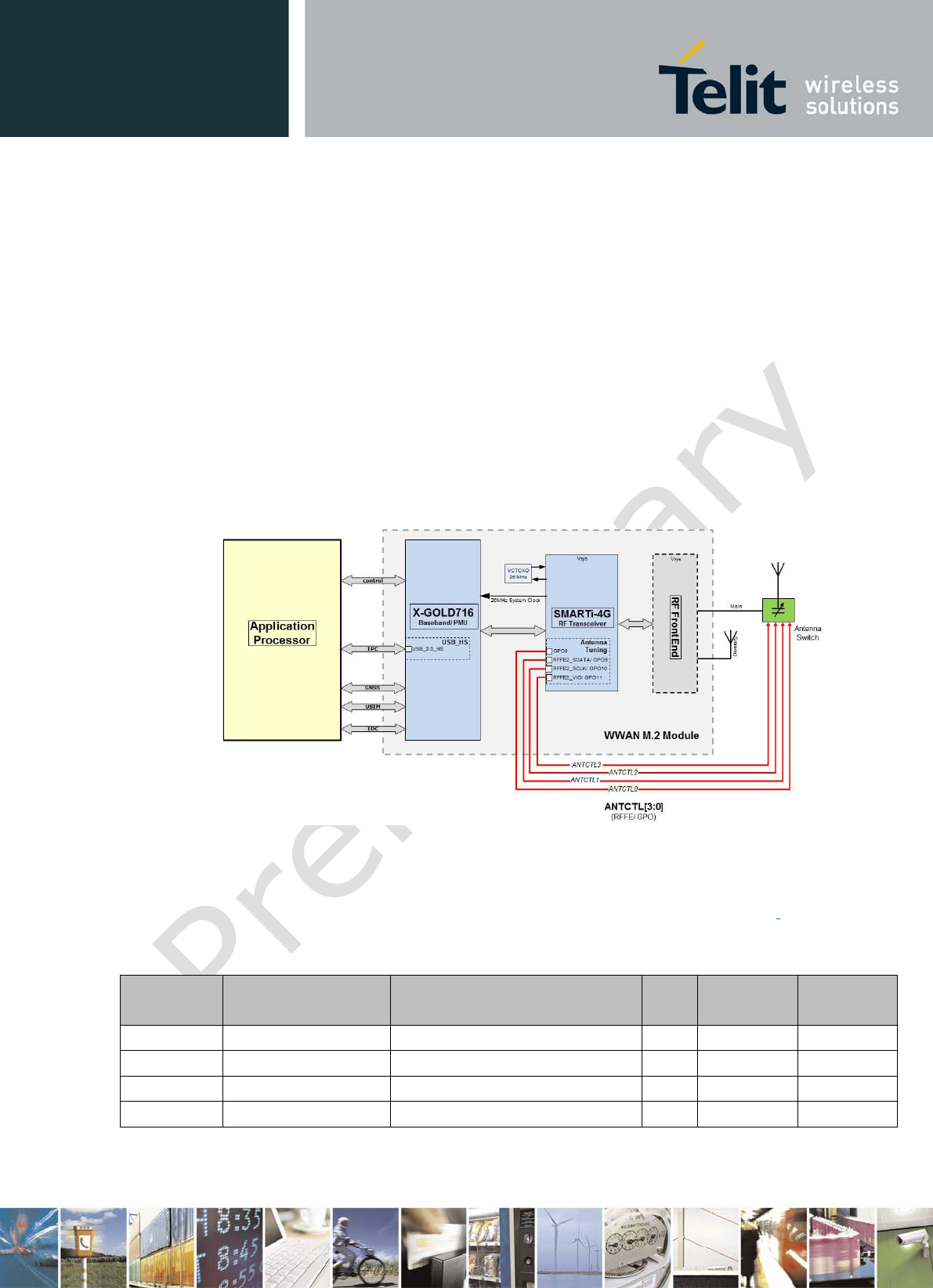
2.3 Host Interface Signals
This section describes the signals available to the host processor at the 75 pin application
interface. Eight signals are eliminated by the notch on the host connector, leaving 67 usable
signals. A diagram of the M.2 module identifying the 75 pin interface is shown in Figure 5.
Note that the M.2 module has all components mounted on the top side. Odd pin numbers are on the top
side while even pins on the bottom side.
Reproduction forbidden without written authorization from Telit Communications S.p.A. - All Rights Reserved. Page 21 of 77
xN930 M.2 Hardware User Guide
1VV0301078 Rev.6 – 2013-11-12
Figur e 5 PCI Ex pr e ss M .2 Module I nt e rfa ce
A complete description of all interface signals available at the host interface is listed in Table
4. Some features, such as GNSS and Antenna Tuning, are not available on every M.2 module.
On those modules, the signals at the application interface are not connected on the M.2
module.
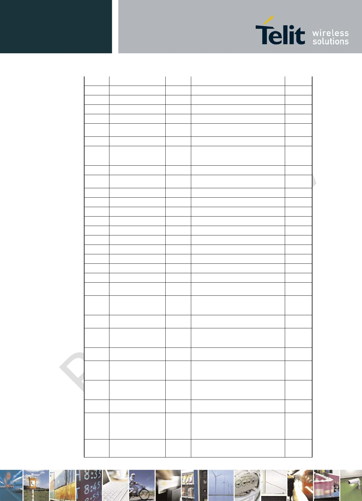
Ta ble 4 M .2 Host I nte rface Signa ls
Pin
Signa l N a m e
I / O
D escr ipt ion
Supply
1
CONFI G_3 O Presence I ndication:
WWAN M.2 Connect s t o GND
int ernally
-
2
3.3V
P
M.2 Supply Pin 3.3 V
3.3 V
3
GND
P
Ground
-
4
3.3V
P
M.2 LTE Supply Pin 3.3 V
3.3 V
5
GND
P
Ground
-
6
Card_Power_On_Off
I
Cont rol signal to power On/ Off
M.2.
1.8 V
7
USB D+
I O
USB 2.0 HS DPLUS Signal
1.8
V/ 2.9 V
Pin
Signa l N a m e
I / O
D escr ipt ion
Supply
8
W_DI SABLE#
I
Act ive low signal t o Disable Radio
Oper at ion
3.3 V
Reproduction forbidden without written authorization from Telit Communications S.p.A. - All Rights Reserved. Page 22 of 77
xN930 M.2 Hardware User Guide
1VV0301078 Rev.6 – 2013-11-12
9
USB D–
I O
USB 2.0 HS DMI NUS Signal
1.8
V/ 2.9 V
10
LED# 1
O
Open Drain, activ e low signal used
for add-in car d t o pr ov ide st atus
3.3 V
11
GND
P
Ground
-
12
SLOT KEY
13
SLOT KEY
14
SLOT KEY
15
SLOT KEY
16
SLOT KEY
17
SLOT KEY
18
SLOT KEY
19
SLOT KEY
20
AUDI O0 I O PCM Clock ( I 2S_CLK) - Fut ure
developm ent
1.8 V
21
CONFI G_0 O Configurat ion St at us. Present ly
not connect ed on WWAN M.2
m odule.
-
22
AUDI O1 I PCM I n ( I 2S_RX) - Fut ure
developm ent
1.8 V
23
WAKE_WWAN#
O
Wak e On WWAN
Use by M.2 t o w ake up host .
1.8 V
24
AUDI O2 O PCM Out (I 2S_TX) - Future
developm ent
1.8 V
25
DPR#
I
Dy nam ic Power Reduction - Body
SAR control signal
1.8 V
26
GNSS_DI SABLE#
I
Disable GNSS funct ion
1.8 V
27
GND
P
Ground
-
28
AUDI O3 I O PCM Sync ( I 2S_WA0) - Future
developm ent
1.8 V
29
N/ C
-
Not connect ed internally on M.2
-
30
UI M-RESET
O
SI M Reset ( I )
1.8
V/ 2.9 V
31
N/ C
-
Not connect ed internally on M.2
-
32
UI M-CLK
O
SI M Clock ( I )
1.8
V/ 2.9 V
33
GND
-
Ground
-
34
UI M-DATA
I O
SI M Dat a ( I / O)
1.8
V/ 2.9 V
35
N/ C
-
Not connect ed internally on M. 2
-
Pin
Signa l N a m e
I / O
D escr ipt ion
Supply
36
UI M-PWR
O
SI M pow er ( 1.8 V/ 2.9 V)
1.8
V/ 2.9 V
37
N/ C
-
Not connect ed internally on M.2
-
38
N/ C
-
Not connect ed internally on M.2
-
Reproduction forbidden without written authorization from Telit Communications S.p.A. - All Rights Reserved. Page 23 of 77
xN930 M.2 Hardware User Guide
1VV0301078 Rev.6 – 2013-11-12
39
GND
P
Ground
-
40
I 2C_SCL
I O
I 2C Clock – GNSS Support
1.8 V
41
N/ C
-
Not connect ed internally on M.2
-
42
I 2C_SDA
I O
I 2C Data – GNSS Support
1.8 V
43
N/ C
-
Not connect ed internally on M.2
44
I 2C_I RQ
I
GNSS I nt errupt Request – GNSS
Support
1.8 V
45
GND
P
Ground
-
46
SYSCLK
O
26 MHz reference Clock out put for
ext er nal GNSS
m odule
1.8 V
47
N/ C
-
Not connect ed internally on M.2
-
48
TX_BLANKI NG
O
GNSS Blank ing Signal used t o
indicat e 2G Tx burst.
1.8 V
49
N/ C
-
Not connect ed internally on M.2
-
50
N/ C
-
Not connect ed internally on M.2
-
51
GND
P
Ground
-
52
N/ C
-
Not connect ed internally on M.2
-
53
N/ C
-
Not connect ed internally on M.2
-
54
N/ C
-
Not connect ed internally on M.2
-
55
N/ C
-
Not connect ed internally on M.2
-
56
N/ C
-
Not connect ed internally on M.2
-
57
GND
P
Ground
-
58
N/ C
-
Not connect ed int er nally on M.2
-
59
ANTCTL0
I
RF Ant enna Tuning Cont rol Signal
0
1.7 V -
2.6 V
60
COEX0
-
Wireless Coexist ence between
WWAN and WiFi/ BT
m odules
-
61
ANTCTL1
I
RF Ant enna Tuning Cont rol Signal
1
1.7 V -
2.6 V
62
COEX1
-
Wireless Coexist ence bet w een
WWAN and WiFi/ BT
m odules
-
63
ANTCTL2
I
RF Ant enna Tuning Cont rol Signal
2
1.7 V -
2.6 V
64
COEX2
Wireless Coexist ence between
WWAN and WiFi/ BT
m odules
-
Pin
Signa l N a m e
I/O
D escr ipt ion
Supply
65
ANTCTL3
I
RF Ant enna Tuning Cont rol Signal
3
1.7 V -
2.6 V
66
SI M DETECT
I
SI M Card Det ect ion (I ) (low
act iv e) .
• Pull-up resist or on WWAN M.2
m odule
1.8 V
67
RESET#
I
Single cont rol to r eset WWAN (O)
( * not used on ULTRABOOK
designs)
1.8 V
Reproduction forbidden without written authorization from Telit Communications S.p.A. - All Rights Reserved. Page 24 of 77

xN930 M.2 Hardware User Guide
1VV0301078 Rev.6 – 2013-11-12
68
N/ C
-
Not connect ed internally on M.2
-
69
CONFI G_1 O Configur ation Stat us
WWAN M.2 Connect s t o GND
int ernally
-
70
3.3V
P
WWAN Supply Pin 3.3 V
-
71
GND
P
Ground
-
72
3.3V
P
WWAN Supply Pin 3.3 V
-
73
GND
P
Ground
-
72
3.3V
P
WWAN Supply Pin 3.3 V
-
75
CONFI G_2 O Configurat ion St at us
WWAN M.2 Connect s to GND
int ernally
-
Reproduction forbidden without written authorization from Telit Communications S.p.A. - All Rights Reserved. Page 25 of 77

xN930 M.2 Hardware User Guide
1VV0301078 Rev.6 – 2013-11-12
3 M.2 Module Interface Details
This section provides details on the various interfaces available M.2 modules.
3.1 USB 2.0 High-Speed – IPC Interface
The host processor, connected via a USB 2.0 High-speed interface, has access to the
functions of the WWAN card. The USB port is the interprocessor communications
interface with the host system.
The device classes supported are: CDC-MBIM, CDC-ACM, and CDC-NCM.
The USB Controller is compliant to the USB 2.0 Specification and with the Link Power
Management (LPM) Addendum. LPM introduces a new sleep state (L1) which significantly
reduces the transitional latencies between the defined power states; hence, improving the
responsiveness of the WWAN platform regarding connecting to the internet (Quick Connect).
• USB2.0 LPM L1 Support
• Support for OS assisted fast dormancy
• Selective Suspend support
• Very low power when in Selective Suspend: <4mw when connected
to network (wake), <1 mW no wake
It supports High-speed (HS, 480 MBit/s); Full-speed (FS, 12 MBit/s) transfers. Low- speed
mode is not supported. Because there is not a separate USB-controlled voltage bus, USB
functions implemented on the M.2 module are expected to report as self-powered devices
General Features
• In device mode : High-speed (480 MBit/s) and Full-speed (12 MBit/s)
• In host mode: High-speed (480 MBit/s), Full-speed (12 MBit/s). Low-speed mode (1.5
Mbit/s) is not supported.
• Support for 16 bidirectional end points and channels including the end point 0.
Ta ble 5 USB H S I nt e rproce ssor Com mun ica tion s I n
t e r
face
Signa l N a m e
D escr ipt ion
Pin
D ir ect ion
( W W AN )
Volt a ge
Level
USB_D+
USB Data Plus
7
I , O
2.85 V
USB_D–
USB Dat a
Minus
9
I , O
2.85 V
Reproduction forbidden without written authorization from Telit Communications S.p.A. - All Rights Reserved. Page 26 of 77
xN930 M.2 Hardware User Guide
1VV0301078 Rev.6 – 2013-11-12
3.2 (U)SIM Interface
An external SIM Card socket is assumed to be mounted on the system board. The
M.2 module will access the SIM card through its USIM interface.
The USIM interface is compatible with the ISO 7816-3 IC Card standard on the issues
required by the GSM 11.12 and GSM 11.18 standard.
Both 1.8 V and 3 V SIM Cards are supported.
A few comments on the SIM_DETECT signal
1. An external pull-up resistor is not needed on SIM_DETECT. An internal pull-up
resistor on X-GOLD™ baseband IC will be used.
2. When a SIM is inserted, SIM_DETECT will be high.
3. When a SIM is removed or not present, SIM_DETECT will be low.
4. The host does not need to drive this signal. It can be tri-stated.
Ta ble 6 ( U) SI M I nt e rfa ce Sign a ls
Signa l N a m e
D escr ipt ion
Pin
D ir ect ion
( W W AN )
Volt a ge
Level
UI M_CLK
Clock SI M Card
32
O
1.8 V/ 2.9
V
UI M_DATA
I nput / Out put SI M Card
34
I , O
1.8 V/ 2.9
V
UI M_RESET
Reset signal for SI M card
30
O
1.8 V/ 2.9
V
USI M_PWR
1.8 V/ 3 V Supply for SI M Car d
36
O
1.8 V/ 2.9
V
SI M Detect
SI M Card Det ect ion
66
I
1.8 V
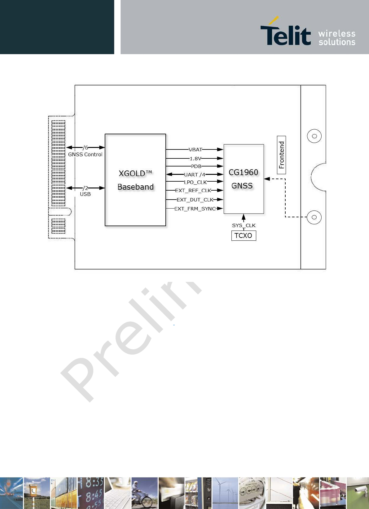
3.3 GNSS Interface
Some M.2 modules incorporate GPS and GLONASS receivers with aGPS to support
Global Positioning.
For M.2 modules that feature GNSS support, see Table 1, the M.2 module incorporates the
CG1960 Single-Chip GNSS Device, which is a complete receiver for simultaneous reception
and processing of both GPS and GLONASS signals. It includes LNA, mixer, bandpass filter,
VCO, ALC, fractional-N frequency synthesizer, digital tunable filters, PGA stage, and multi-
bit ADCs. A UART interface is used by the
X-GOLD™ Communications Processor on the M.2 module to control the GNSS device. The
solution offers best-in-class acquisition and tracking sensitivity, TFF and accuracy.
The GNSS device supports several different power management modes which gives the
lowest possible energy usage per fix. The pre-calculated location data will be sent over the
USB host interface. In addition, the M.2 will produce GPS data when the system is in sleep
mode via an I2C interface to allow for applications to be available in low power modes.
Reproduction forbidden without written authorization from Telit Communications S.p.A. - All Rights Reserved. Page 27 of 77

xN930 M.2 Hardware User Guide
1VV0301078 Rev.6 – 2013-11-12
GNSS General Features
• Autonomous GPS / GLONASS
• Assisted GPS Using SUPL 1.0/2.0
• MS Assisted positioning ( SET / NET Initiated )
• MS Based positioning ( SET / NET Initiated )
• SUPL 2.0 Feature Sets
• Version Negotiation
• Periodic Triggers
• Emergency Positioning
• Area Event Triggers (SET Init & NET Init)
• Application ID
• Enhanced Cell Id
• Multiple Location IDs
• Session Info Query
• Location Transfer to 3rd Party
• Notification Verification Based on Current Location
• Location Request to another SET
A diagram of the GNSS connections on the M.2 module is shown in Figure 6. This diagram
identifies the signals between the X-GOLD™ baseband and GNSS devices along with the
USB and GNSS signals available to the host at the card interface.
Reproduction forbidden without written authorization from Telit Communications S.p.A. - All Rights Reserved. Page 28 of 77
xN930 M.2 Hardware User Guide
1VV0301078 Rev.6 – 2013-11-12
Figur e 6 GN SS Conne ct ions a nd I nt e rfa ce
A description of the signals between the X-GOLD™ baseband and the CG1960
interface are defined in Table 7.
Reproduction forbidden without written authorization from Telit Communications S.p.A. - All Rights Reserved. Page 29 of 77
xN930 M.2 Hardware User Guide
1VV0301078 Rev.6 – 2013-11-12
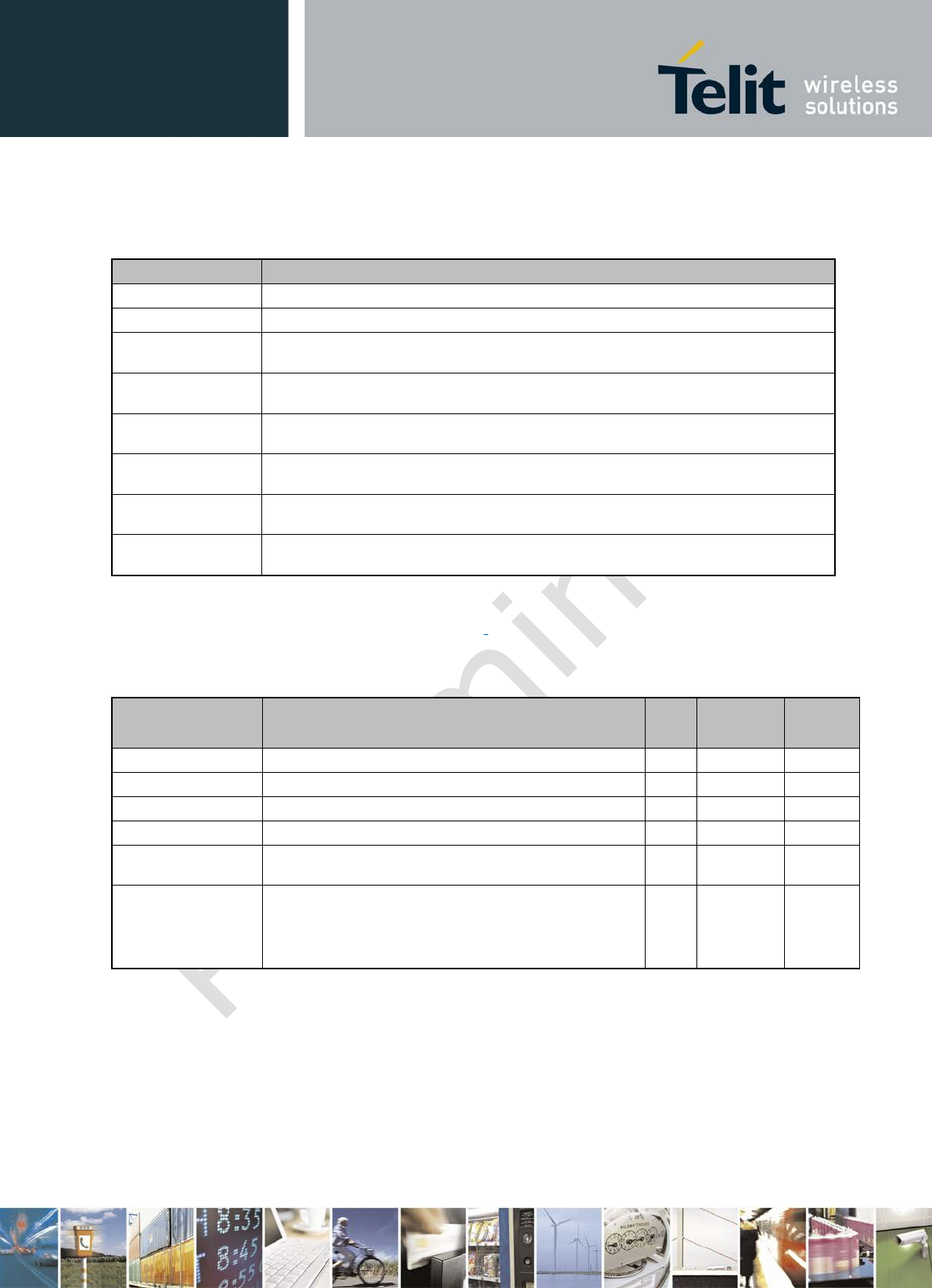
Ta ble 7 X- GOLD ™ Base ba nd t o GN SS I nt e rfa ce Signals
Signal
Description
VBAT
Battery Supply
1.8V
1.8 V Supply provided from X-GOLD™ Baseband
UART
The data and control I/F between the X-GOLD™ baseband and the GNSS
device is over a 4 wire UART interface which include CTS/RTS handshaking.
PDB
X-GOLD™ baseband uses this signal to control Power-on/reset of the GNSS
device
LPO_CLK
X-GOLD™ baseband provides a permanently active 32 kHz clock to the GNSS
device
EXT_REF_CLK
X-GOLD™ baseband provides a 26 MHz clock to the GNSS device for
frequency aiding.
EXT_DUT_CLK
X-GOLD™ baseband provides this signal to notify the GNSS device of that
GSM Tx activity (PA Blanking)
EXT_FRM_SYNC
X-GOLD™ baseband provides a strobe signal to the GNSS device to allow fine
time assistance based on 3GPP cell timing.
The GNSS signals available to the host at the WWAN module interface to support
GNSS operation are shown in Table 8.
Ta ble 8 GN SS M odu le I nt e rfa ce Sign a ls
Signal Name
Description
Pin
Direction
(WWAN)
Voltage
Level
I2C_SCL
I2C Clock
40
I, O
1.8 V
I2C_SDA
I2C Data
42
I, O
1.8 V
I2C_IRQ
I2C IRQ - Interrupt signal
44
I
1.8 V
SYSCLK
Synchronization Clock
46
I
1.8 V
TX_BLANKING
TX Blanking – Active High when M.2 is
transmitting.
48
O
1.8 V
GNSS_DISABLE#
GNSS Disable
• High: GNSS function is determine by AT
command.
•
Low: GNSS function is disabled.
26
I
1.8 V
3.4 System Control Interface
The system control interface is used to control the power-up and reset of the WWAN
module. There are additional control signals to disable the radio, drive an LED as a status
indicator, an output to wake the host processor, and an input for body SAR.
Reproduction forbidden without written authorization from Telit Communications S.p.A. - All Rights Reserved. Page 30 of 77
xN930 M.2 Hardware User Guide
1VV0301078 Rev.6 – 2013-11-12
3.4.1 Power On & Reset
The host processor has two signals that can be used to power on and reset the modem.
Powering off the modem is accomplished through an AT command.
Ta ble 9 Pow e r- on & Reset Sign als
Signal Name
Description
Pin
Direction
(WWAN)
Voltage
Level
Card_Power_ON_OFF
Modem power on: For Tablet based designs
only; this signal is used for power on-off control of
X-GOLD™ Baseband IC.WWAN M.2 module
• Logic Low: M.2 Off
• Logic High: WWAN M.2 Power On
This pin has an internal pull-down resistor.
Ultrabook designs:
Ultrabook host should deliver a 1.8V signal to turn on
the module. If 1.8V is not feasible, recommend using a
47k series resistor connected to 3.3V.
6
I
1.8 V
RESET#
Reset the WWAN system. For Tablet based designs,
this signal is used to reset the module.
• Asynchronous, active low signal. When
active, the WWAN M.2 module will be placed
in a power–on reset condition.
Ultrabook designs, this signal is not used.
67
I
1.8 V
3.4.2 Host Radio Disable Operation
An additional control signal is used to disable the radio on the module.
Signal W_DISABLE# is provided to allow users to disable, via a system-provided switch,
the add-in card’s radio operation in order to meet public safety regulations or when
otherwise desired. Implementation of this signal is required for systems and all add—in
cards that implement radio frequency capabilities.
The W_DISABLE1 signal is an active low signal that when driven low by the system shall
disable radio operation. The assertion and de-assertion of the W_DISABLE# signal is
asynchronous to any system clock. All transients resulting from mechanical switches need to
be de-bounced by the host system and no further signal conditioning will be required. When
the W_DISABLE# signal is asserted, all radios attached to the add-in card shall be disabled.
When the W_DISABLE# is not asserted or in a high impedance state, the radio may transmit
if not disabled by other means such as software.
The operation of the W_DISABLE# Signal is:
Reproduction forbidden without written authorization from Telit Communications S.p.A. - All Rights Reserved. Page 31 of 77
xN930 M.2 Hardware User Guide
1VV0301078 Rev.6 – 2013-11-12
Enable, ON (3.3V): The radio transmitter is to be made capable of transmitting. Disable,
OFF (low): The radio transmitter(s) is to be made incapable of transmitting.
Standard TTL signaling levels shall be used making it compatible with 1.8 V and 3.3 V
signaling.
W_DISABLE# pin has a pull-up resistor on the M.2 module.
Ta ble 1 0 Ra dio Disa ble Sign al
Signal Name
Detailed Description
Pin
Direction
(WWAN)
Voltage
Level
W_DISABLE#
Disable Radio. This active low signal
allows the host to disable the M.2 radio
operation in order to meet public safety
regulations or when otherwise desired.
• Logic Low: M.2 Off
• Logic High: function is
determined by Software (AT
Command).
If this pin is left un-connected,
functionality is controlled by software.
Care should be taken not to activate this
pin unless there is a critical failure and
all other methods of regaining control
and/or communication with the M.2
module have failed.
8
I
Compatible
with
1.8 V/3.3
V
Standard TTL signaling levels shall be used.
Reproduction forbidden without written authorization from Telit Communications S.p.A. - All Rights Reserved. Page 32 of 77

xN930 M.2 Hardware User Guide
1VV0301078 Rev.6 – 2013-11-12
Ta ble 1 1 H ost Ra dio Disa ble I nt e rf a ce ( W _ DI SABLE# )
Requirement
Detailed Description
Radio disable duration
On reception of a HW or SW disable signal, the WWAN module
will initiate within one second the mandatory cellular procedures
(which are dependent on current state) for disconnecting from
the cellular network. The time taken to complete the procedures
will be dependent on external factors including but not limited
to:
3G/4GPP specifications, network implementation, radio
conditions, etc. Once those procedures are complete, the WWAN
module will switch off the RF.
Radio enable duration
On reception of a hardware or software enable signal the
WWAN module will initiate within one second the mandatory
cellular procedures for connecting to the cellular network.
Radio enable during selective suspend
If radio is disabled due to W_DISABLE# assertion and WWAN
module is in selective suspend, then W_DISABLE# de-assertion
shall be detected by WWAN module and the module shall
initiate exit from selective suspend.
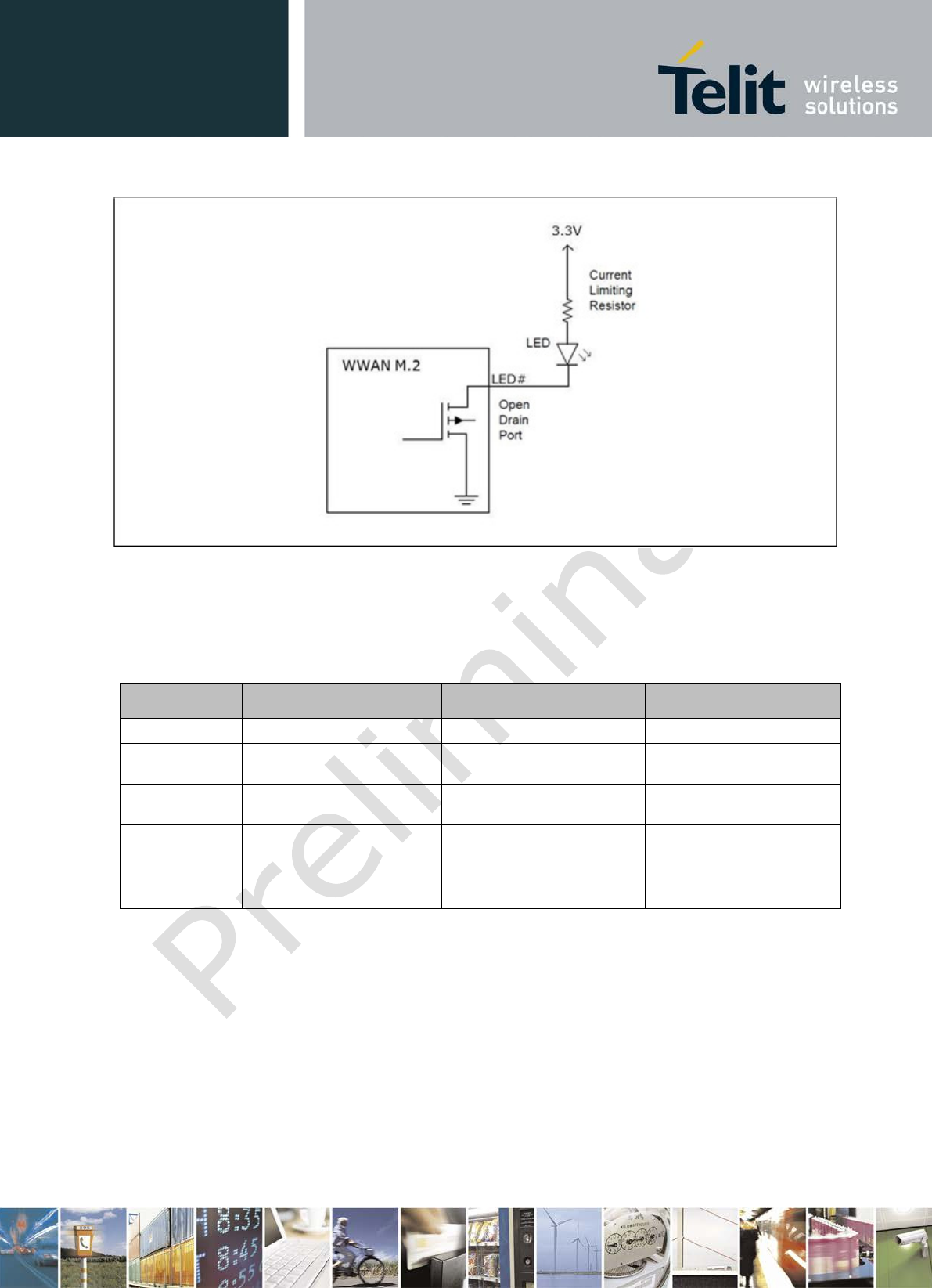
3.4.3 LED Interface – Status Indicator
An LED will be used to provide status indications to users via system provided
indicators.
LED#1 (pin 10) is an active low output signal intended to drive system-mounted LED
indicators. These signals shall be capable of sinking to ground a minimum of 9.0 mA at up to
a maximum VOL of 400 mV. The LED has four defined states.
Ta ble 1 2 LED # 1 Signa l
Signal Name
Detailed Description
Pin
Direction
(WWAN)
Voltage
Level
LED#1
LED Status Indicator
10
O (OD)
3.3 V
Figure 7 is an example of how an LED indicator is typically connected in a platform/system
using 3.3 V. The series resistor can be adjusted to obtain the desired brightness.
Reproduction forbidden without written authorization from Telit Communications S.p.A. - All Rights Reserved. Page 33 of 77
xN930 M.2 Hardware User Guide
1VV0301078 Rev.6 – 2013-11-12
Figur e 7 Ty pica l LED Con ne ct ion
The indication protocol for the LED is shown in Table 13.
Ta ble 1 3 LED Sta t e I ndica t or
State
Definition
Characteristics
WWAN
S
OFF
The LED is emitting no
-
Not
ON The LED is emitting light
in a stable non-flashing
- Powered registered but
not transmitting or
Slow Blink The LED is flashing
at a steady but slow
250 ±25% ms ON period.
0.2 ± 25% Hz blink rate
Activity proportional to
transmitting/ receiving
Intermediate
Blink
The LED is flashing
intermittently proportiona
l
to the activity on the
interface
50% duty cycle, 3 Hz
minimum blink rate, 20 H
z
maximum blink rate
-
3.4.4 Wake on WWAN Signal
An output signal is available to wake the host system, WWAN_N. This is an active low,
open-drain output.
This output requires a pull-up resistor on the host system.
Reproduction forbidden without written authorization from Telit Communications S.p.A. - All Rights Reserved. Page 34 of 77
xN930 M.2 Hardware User Guide
1VV0301078 Rev.6 – 2013-11-12
Ta ble 1 4 W ak e on W W AN Signal
Signal Name
Detailed Description
Pin
Direction
(WWAN)
Voltage
Level
WAKE_WWAN# Used by M.2 module to wake the
host. Active Low, Open Drain output
23 O (OD) 3.0 V
3.4.5 Dynamic Power Reduction
With the arrival of Tablets and Ultrabook™ platforms where the antenna is in the base of the
unit, there is a significant issue passing Specific Absorption rate (SAR) requirements for
certification.
The WWAN M.2 module has the ability to configure RF TX power levels based on
proximity sensor input from the host.
A WWAN M.2 power control API is available to the host to dynamically reduce RF
transmit power levels of the WWAN module based on proximity sensor input from the
host.
The DPR# (Dynamic Power Reduction) signal is available on the host interface to assist in
meeting regulatory SAR (Specific Absorption Rate) requirements for RF exposure.
Reproduction forbidden without written authorization from Telit Communications S.p.A. - All Rights Reserved. Page 35 of 77

xN930 M.2 Hardware User Guide
1VV0301078 Rev.6 – 2013-11-12
Ta ble 1 5 DPR# / SAR Su pport Sign a l
Signal Name
Detailed Description
Pin
Direction
(WWAN)
Voltage
Level
DPR# Dynamic Power reduction.
25 I 1.8 V
Reproduction forbidden without written authorization from Telit Communications S.p.A. - All Rights Reserved. Page 36 of 77
xN930 M.2 Hardware User Guide
1VV0301078 Rev.6 – 2013-11-12
3.5 Tunable Antenna Control Interface
In notebook platforms, since the WWAN antennas are usually located on the top of the lid,
there is a long RF mini-coax cable that can be up to 60 cm long between the antenna and
WWAN module, it is preferred to use switches/tunable components directly on the antenna
for antenna band switching/tuning to improve efficiency.
On select WWAN M.2 modules, four (4) GPOs are available on the host interface that can be
connected to an external antenna switch, to load the antenna with different impedances,
configuring the different frequency responses for the main antenna. A sample block diagram
depicting the antenna control signal connections to the antenna switch is shown in Figure 8
Intel’s current antenna control solution offers an open loop control solution. The WWAN
M.2 modem expects the AP to provide the antenna profile detection and through a pre-
defined API, notify the WWAN M.2 modem with the correct antenna profile. The WWAN
M.2 modem then applies the proper antenna profile data accordingly.
Figur e 8 Ant en na Con tr ol – Conne ct ion s De ta il
The electrical specification for the antenna control GPIOs are shown in Table 16.
Ta ble 1 6 Tuna ble Ant e nn a Cont rol Sign als
Signal
Name
Description Smarti™ 4G Signal
Pin
Direction
(WWAN)
Voltage
Level
ANTCTL0
Antenna Control 0
GPO8
59
O
1.7 – 2.6 V
ANTCTL1
Antenna Control 1
RFFE2_SDATA/ GPO9
61
O
1.7 – 2.6 V
ANTCTL2
Antenna Control 2
RFFE2_SCLK/ GPO10
63
O
1.7 – 2.6 V
ANTCTL3
Antenna Control 3
RFFE2_VIO/ GPO11
65
O
1.7 – 2.6 V
Reproduction forbidden without written authorization from Telit Communications S.p.A. - All Rights Reserved. Page 37 of 77
xN930 M.2 Hardware User Guide
1VV0301078 Rev.6 – 2013-11-12
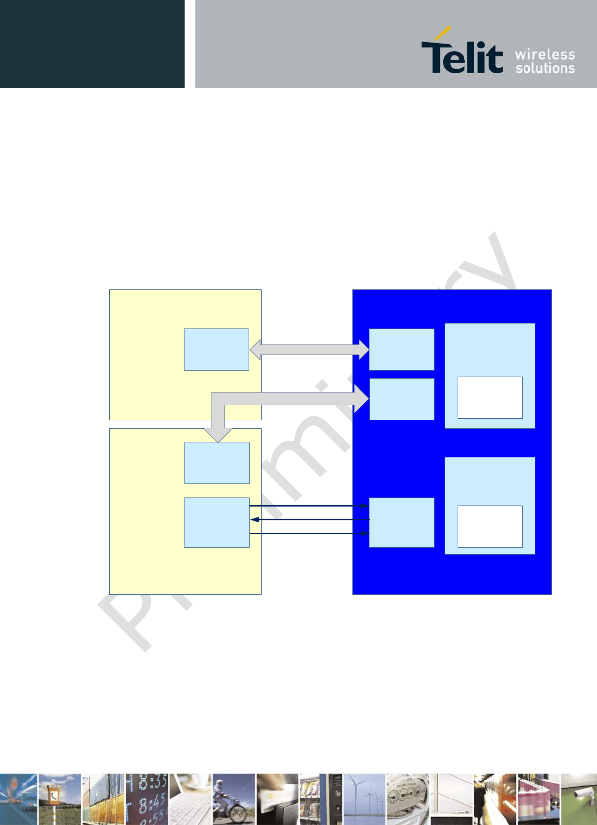
3.6 In-Device Coexistence Interface
As more and more radios are added to PC Ultrabook™ and tablet platforms, the sources RF
interference increases significantly as multiple radios will have overlapping transmissions
and receptions. This problem will increase further as overlapping bands continue to be rolled
out; WIFI, BT, WWAN will all use overlapping band from 2300 MHz to 2600 MHz.
In-Device Coexistence is a feature which improves the user experience and maximizes
throughput and Quality of Service of connectivity systems (WLAN, BT and GNSS) when
these radios are simultaneously running with the WWAN M.2 LTE modem.
A diagram of the In-Device Coexistence architecture is shown in Figure 6.
Application
Processor
apps
coexistence
interface
Connectivity Chip
(WLAN/BT/GNSS)
NRT
Coexistence
interface
RT
Coexistence
interface
X-GOLD™ 716
apps
coexistence
interface
NRT
Coexistence
interface
RT
Coexistence
interface
CPU
NRT
coexistence
controller
LTE L1
RT
coexistence
controller
Message –based I/F)
IDC_CwsPriority
NRT Apps Coex I/F
Message –based I/F)
NRT Coex I/F
IDC_LteFrameSync
IDC_LteDtxEnv
Figur e 9 I n-D e vice Coe xist ence Archit ect ure
Seamless Co-running
In-Device-Coexistence primarily aims at avoiding interference between radio systems to
allow seamless co-running where LTE and WLAN/BT/GNSS ensuring their maximum
throughput and performance. To do so, a Non Real Time (NRT) coexistence controller is
implemented on the ARM™ CPU. The NRT coexistence controller centralizes LTE, WLAN,
BT and GNSS information and performs interference avoidance mechanisms, selecting
interference-safe frequency configurations whenever possible. The NRT coexistence
controller is also in charge of enabling some Real Time (RT) coexistence mechanisms when
Reproduction forbidden without written authorization from Telit Communications S.p.A. - All Rights Reserved. Page 38 of 77
xN930 M.2 Hardware User Guide
1VV0301078 Rev.6 – 2013-11-12
NRT mechanisms are not sufficient to guarantee seamless co-running of LTE and
connectivity systems (WLAN, BT, and GNSS).
Inter-system Synchronization
For the cases where co-running of LTE and connectivity systems cannot be achieved, a Real
Time (RT) coexistence controller is implemented in the LTE Layer-1 subsystem. The RT
coexistence controller is in control of the RT coexistence interface, which is exposed to the
connectivity chip. The RT coexistence controller exploits real time information received from
the LTE Layer-1 subsystem and from the connectivity chip to coordinate LTE and
connectivity “in the air” activities. The coordination function protects LTE traffic while
optimizing the throughput and availability of WLAN/BT/GNSS. When operating in this mode,
the connectivity systems have reduced capability since they access the medium when LTE is
inactive, or when their respective operations do not impact each other significantly.
The Non Real-Time mechanism implements a messaging based interface, formatted as AT
commands that are passed to the AP host over the IPC interface (USB). A simple piece of SW
residing on the AP host will tunnel the Non Real-Time messages between the BT/WLAN
device and M.2 module, translate AT commands to/from the BT/WLAN driver commands,
and maintain the states of the BT/ WLAN and M.2 LTE modem. The host software will also
be responsible for initializing the Real-Time mechanism.
The Real-Time mechanism consists of 3 GPIO signals which allow the synchronization of
multiple TX and RX events. The signals to support real Time coexistence are listed in Table
17.
If the coexistence signals are not used by the host system, they should not be
connected.
Ta ble 1 7 Coe x ist e nce – H ardw are Synchr on iz a t ion Signa ls
Signal
Name
Description
Pin
Direction
(WWAN)
Voltage Level
COEX0 IDC_LteDtxEnv - Synchronous signal
indicating LTE UL gap. Envelop signal with
edges occurring 1ms before in-the-air gap
(raising and falling edges)
RT arbiter indicates to connectivity cores
when there is no LTE Tx (Envelope)
60 I/O 1.8 V
COEX1 IDC _CwsPriority - 0 : Low priority / 1 :
high priority CWS Indicates if the coming
activity is high priority
62 I/O 1.8 V
Reproduction forbidden without written authorization from Telit Communications S.p.A. - All Rights Reserved. Page 39 of 77

xN930 M.2 Hardware User Guide
1VV0301078 Rev.6 – 2013-11-12
COEX2 IDC_LteFrameSync - Synchronous signal
indicating LTE frame start.
Indicates LTE frame start to BT/WLAN
device. Can be used by BT to synch up
periodic activity with LTE timing
64 I/O 1.8 V
3.7 Power Supply Interface
The M.2 modules require the host to provide the 3.3 V power source. The voltage source is
expected to be available during the system’s stand-by/suspend state to support wake event
processing on the communications card.
The 3.3 V power and ground pins are listed in Table 18.
Section 8, Power Delivery Requirements, provides electrical requirements for the
power supply and I/O signals.
Ta ble 1 8 Pow e r & Gr oun d Sign a ls
Power Pins
Description
2, 4, 70, 72, 74
3.3 V Supply
3, 5, 11, 27, 33, 39, 45, 51, 57, 71, 73
Ground
3.8 Trace & Debug Interface
The USB port on the M.2 module will be used to support system tracing of the Protocol
stack. The USB port is also used for software download and manufacturing testing.
The JTAG & MIPI PTI1 ports are accessible on the module to support system debug. A
temporary cable assembly over flat flex should be assembled on bottom of the module and
lead out of the final product. The cable would not be mounted on the final
product.
Reproduction forbidden without written authorization from Telit Communications S.p.A. - All Rights Reserved. Page 40 of 77
xN930 M.2 Hardware User Guide
1VV0301078 Rev.6 – 2013-11-12
3.9 Configuration Pins
There are 4 configuration pins on the M.2 module. On the host side, the output
CONFIGURATION signals that are tied to GND must be fitted with pull-up resistors.
Ta ble 1 9 M.2 Configur a tion Pin s
Signal Name
Description
Pin
Direction
(WWAN)
Voltage
Level
CONFI G_0 This signal is not connect ed t o t he WWAN M.2
m odule.
21 O -
CONFI G_1 Tied to Ground int er nally on the WWAN M.2
m odule.
69 O 0 V
CONFI G_2 Tied to Ground int er nally on the WWAN M.2
m odule.
75 O 0 V
CONFI G_3 Tied to Ground int er nally on the WWAN M.2
m odule.
1 O 0 V
3.10 Reserved Pins
The M.2 module has a few reserved pins. The Reserve pins cannot be used and should not be
connected on the host platform.
Ta ble 2 0 Rese rved Pins
Pins
Description
20
Reserved for future use (Audio)
22
Reserved for future use (Audio)
24
Reserved for future use Audio)
Reproduction forbidden without written authorization from Telit Communications S.p.A. - All Rights Reserved. Page 41 of 77
xN930 M.2 Hardware User Guide
1VV0301078 Rev.6 – 2013-11-12
3.11 No Connect Pins
The M.2 has several No Connect pins. The pins are not connected on the
M.2 module.
Ta ble 2 1 N o Connect Pins
Pins
Description
28, 29, 31, 35, 37, 38, 41, 43, 47, 49, 50, 52, 53,
54, 55, 56, 58, 68
No Connect Pins
10, 11, 12, 13, 14, 15, 16, 17, 18, 19
Notch
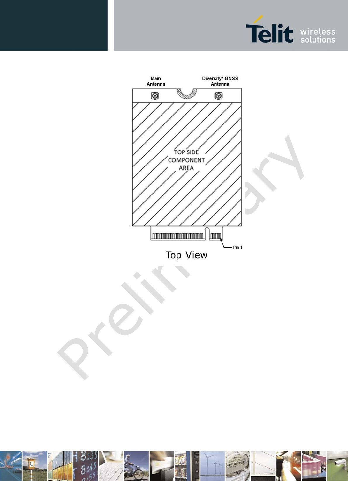
3.12 Antenna Interface
The M.2 module will have two antenna connectors, a main Rx/Tx antenna and a secondary
antenna that will be multiplexed between the Diversity receiver and GPS receiver (if
applicable).
The antenna signals are not available at the host interface but have their own
connectors. A diagram on the M.2 module with the location of the RF connectors
appears in Figure 10.
Ta ble 2 2 Ant e nna Re quire m ent s
Requirement
Detailed Description
Connection
to module
The connector of WWAN antenna cable is Hirose W.FLT or equivalent
Multi-band
single antenna
Single antenna has to support all bands of WWAN module specified in the
Product
Rx
Diversity
Diversity antenna has to support all bands WWAN module specified in the
Product
GPS Antenna
The GPS antenna will share the Diversity antenna connector.
Reproduction forbidden without written authorization from Telit Communications S.p.A. - All Rights Reserved. Page 42 of 77

xN930 M.2 Hardware User Guide
1VV0301078 Rev.6 – 2013-11-12
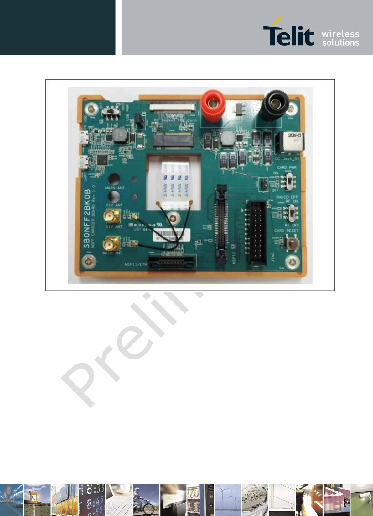
4 Development Tools
Intel Mobile Communications provides a carrier development board to facilitate system test
and verification of the M.2 module. In addition, a set of comprehensive tools to enable rapid
integration and customization of the M.2 software is provided.
The hardware and software tools for M.2 development are summarized below.
4.1 Carrier Board
The M.2 Carrier Board, shown in Figure 11, is Intel Mobile Communications hardware
platform to facilitate the test and verification on the M.2 module. Once the M.2 module is
mounted on the Carrier board, the user has access to all necessary interfaces on the module
(host interface signals, debug and trace, and antenna) allowing full system test, debugging,
and diagnostics.
Reproduction forbidden without written authorization from Telit Communications S.p.A. - All Rights Reserved. Page 44 of 77
xN930 M.2 Hardware User Guide
1VV0301078 Rev.6 – 2013-11-12
Figur e 1 1 M . 2 Ca r rier Board
4.1.1 FlashTool
Intel Mobile Communications provides a utility program called FlashTool for
downloading a binary image into the Flash memory of the M.2 module. The USB-HS port
or USIF on the platform is used for connection to a PC via a USB cable for flashing.
FlashTool is a Win32/64 application built on top of the dynamic link library,
Download.DLL.
4.1.2 PhoneTool
PhoneTool is a development tool built on top of the so-called “production test dll,
DWDIO.dll”. PhoneTool can be used to fine tune the parameters of:
• Audio configuration and settings (if enabled on M.2 module)
• NV (Non-Volatile) memory
Reproduction forbidden without written authorization from Telit Communications S.p.A. - All Rights Reserved. Page 45 of 77

xN930 M.2 Hardware User Guide
1VV0301078 Rev.6 – 2013-11-12
• RF power ramp
• Security data IMEI
• SIM
• Real Time Clock
It also includes interfaces for:
• AT Terminal for sending and receiving AT commands.
• DWDIO interface for manual access to the production test dll DWDIO.dll.
• Generic Test Interface (GTI) for RF calibration.
4.1.3 System Trace Tool
System Trace Tool (STT) allows capturing trace sub-streams from different sources on
the platform in one combined stream.
Depending on the trace interface bandwidth, the combined data stream can be sent either
over one of the standard communication interfaces (e.g. USB) or over a dedicated high-
speed MIPI trace interface.
Captured trace data includes standard 3GPP IPC messages, print statements inserted by
developers in the code, error messages, and core dump (crash) information. The actual
decoding of the trace data is done by pluggable decoder libraries, DLL’s and scripts,
which are specific to the version of the mobile station software from which the trace is
captured.
The STT application has a GUI (Graphical User Interface) which provides an easy to use
graphical interface to view, search and analyze trace data. It supports advanced message
filtering runs on all Microsoft Windows® platforms.
STT will become the only tool for trace analysis in the future, the legacy trace tools,
Mobile Analyser and Artemis, will be continue to be supported for the 2G/3G WWAN
M.2 HSPA+ module.
4.1.4 RF Calibration
XMMCalTool is a utility program that can be used for RF calibration. XMMCalTool
supports the following features:
• Optimized calibration
• 3G TX closed loop power control
• Parallel calibration 2G low/high band
• Non-signaling verification
• Industry leading fast sequenced test concept
• Supports parallel RX and TX verification
• Proven Single-Ended BER for faster BER
• < 4 sec/per channel for 3G fast verification (BER, RSSI, TX, ILPC)
Tester supported: R&S CMU200, CMW500, and Agilent 8960
Reproduction forbidden without written authorization from Telit Communications S.p.A. - All Rights Reserved. Page 46 of 77

xN930 M.2 Hardware User Guide
1VV0301078 Rev.6 – 2013-11-12
4.1.5 Noise Profiling Scan Tool
M.2 modules are marketed for use on Tablet, Ultrabook, and Laptop devices. OEM
vendors routinely offer multiple hardware configurations for the same base model, with
different processor speed, drive type, or display type, etc. Each configuration has a
different Radio Frequency emission profile with the possibility of introducing new
interference sources to a modem module.
The Noise Profiling Tool will measure, record down & plot graph of the RF noise level
present on each RX channel. This SW tool will switch on receiver port and sweep all
applicable RX channels on each band and each technology (WiFi, Bluetooth, GPS, and
GLONASS). This will allow OEM vendors to quickly know the noise jamming profile to the
modem module plugged in their devices.
Reproduction forbidden without written authorization from Telit Communications S.p.A. - All Rights Reserved. Page 47 of 77

xN930 M.2 Hardware User Guide
1VV0301078 Rev.6 – 2013-11-12
4.1.6 GNSS Tools
The main functionality provided by the GNSS tool is:
• I/O settings for NMEA port
• Signal quality monitoring
• Time to First Fix measuring control
• Compute Circular Error probability
• SUPL server setting
• Setup a DP context
• AT command window to exercise GNSS primitives/responses
Reproduction forbidden without written authorization from Telit Communications S.p.A. - All Rights Reserved. Page 48 of 77
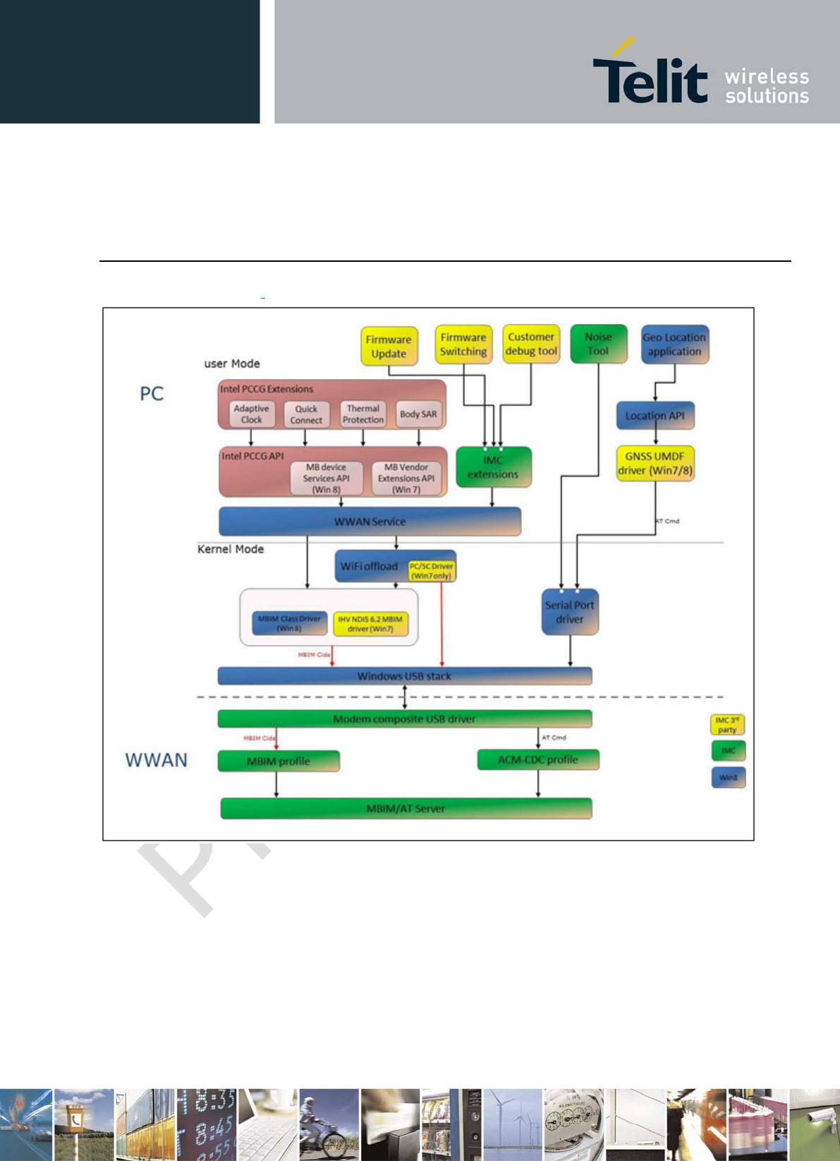
xN930 M.2 Hardware User Guide
1VV0301078 Rev.6 – 2013-11-12
5 Windows Software Components
Figure 12 illustrates the various software components in a Windows based system.
Figur e 1 2 W indow s Soft w ar e Ar chit e ct u re
Reproduction forbidden without written authorization from Telit Communications S.p.A. - All Rights Reserved. Page 49 of 77

xN930 M.2 Hardware User Guide
1VV0301078 Rev.6 – 2013-11-12
5.1 MBIM Toolkit
The following is a summary of software tools provided.
5.1.1 Windows® 7 MBIM driver
In order to support both Windows® 8 and Windows® 7 (for corporate legacy applications),
with a single modem architecture, IMC will provide a kernel level driver implementing the
Mobile Broadband Interface Model. The driver will be WHQL certified for Windows® 7.
5.1.2 GNSS UMDF driver for Windows® 7 and Windows® 8
IMC provides a GNSS "User mode" driver to enable GNSS Applications executing on
Windows PC/Tablet to communicate to the GNSS device located on the M.2 module. The
driver communicates to Modem module via AT commands over an ACM-CDC USB
channel.
5.1.3 M.2 module Firmware Update
This is a “user friendly” Windows GUI application enabling the consumer, whose Ultrabook
or tablet is hosting an Intel M.2 module, to update the firmware on WWAN module by
executing a graphical application based on .NET4 framework. The same application runs on
both Windows® 7 and Windows® 8 environments and its look & feel can be customized if
required.
This same application is used to upgrade the standard image flashed at the factory with one
that better fits the local Carrier. When a new SIM is inserted, the application will detect the
inserted SIM does not match the WWAN device firmware. It will then allow the user to
select and update the WWAN firmware with a suitable image reflecting the local network of
the Carrier.
5.1.4 End User Trace Tool
This is a Windows® 8 application allows a M.2 end user to collect debugging information
under guidance of a Customer Support operator. The log file can be sent to a Technical
support center and fed into an analysis tool, such as Intel’s Mobile Analyzer application, to
diagnose potential problems found in the field after module deployment.
Reproduction forbidden without written authorization from Telit Communications S.p.A. - All Rights Reserved. Page 50 of 77
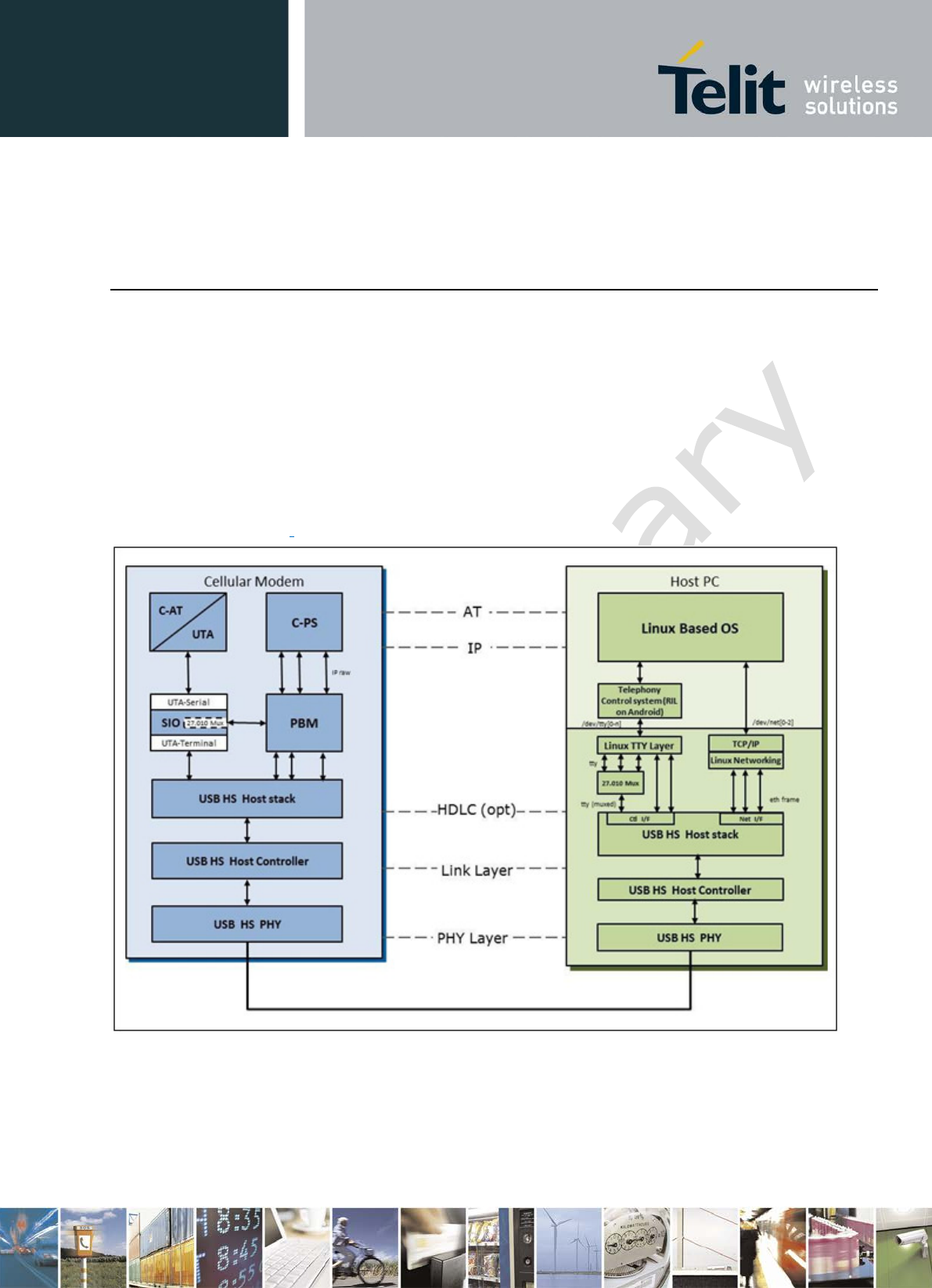
xN930 M.2 Hardware User Guide
1VV0301078 Rev.6 – 2013-11-12
6 Modem Configuration on Linux Based PC
The following section describes the system architecture of Inter-Processor Communication
on a M.2 module when connected to a Linux based Host OS (Android, Chrome, and Ubuntu).
The description is only concerned with the HS-USB port which is the only available
functional interprocessor communications (IPC) interface at run-time and takes into account
only the AT control plane and IP packets data connection. Audio packet exchange is outside
the scope of the current version of M.2.
6.1 Overview
Figure 13 illustrates the architecture of the IPC and its components.
Figur e 1 3 Linux Soft w are Ar chit e ct u re
The user data is transferred from/to the cellular protocol stack (C-PS) to the IPC via a
centralized memory manager. The centralized memory manager is called packet buffer
manager (PBM). The user data is routed along the data plane as IP packets using several
Reproduction forbidden without written authorization from Telit Communications S.p.A. - All Rights Reserved. Page 51 of 77

xN930 M.2 Hardware User Guide
1VV0301078 Rev.6 – 2013-11-12
logical channels. Each logical channel corresponds to a dedicated Packet Data Network
(PDN) connection.
There is no TCP/IP stack on the modem side in the data path from IPC over PBM to
C-PS handling IP address based routing.
The central packet buffer manager (PBM) provides a common packet buffer used between
IPC and PS. No copy operation of data is necessary between cellular PS and IPC. The HS-
USB interface provides a highly efficient data path via DMA with scatter/gather linked-list
processing.
The control plane is using at least one dedicated channel through Serial IO component (S-IO)
to the AT command handler. The interface towards the driver is called Universal Terminal
Adapter (UTA)-Terminal, while the interface towards application is called
UTA-Serial interface. The application in our case is the AT command handler called C-AT. The
control channel is using AT commands. A detailed list of all supported AT commands
can be found in a separate application note.
6.2 CMUX Multiplexer
In the context of an AT command based architecture, a SW multiplexer can be added. The
SW multiplexer of the 3GPP 27.010 protocol provides a number of logical channels (DLC)
which serve as AT terminals on Host PC side. These logical channels are
mapped on-top of one of the control channels of the specific physical IPC interface.
The 3GPP 27.010 multiplexer protocol is a data link protocol (layer-2 of the
OSI mo
d
e
l)
which uses HDLC-like framing, virtual data channels, and channels’ control procedure. The
protocol is implemented according to 3GPP TS27.010. It allows software applications on the
Host processor to access the USB-HS port on M.2 in a concurrent way by emulating multiple
virtual communication channels. The MUX protocol controls the virtual channels and
conveys user data over the virtual channels.
Reproduction forbidden without written authorization from Telit Communications S.p.A. - All Rights Reserved. Page 52 of 77

xN930 M.2 Hardware User Guide
1VV0301078 Rev.6 – 2013-11-12
6.3 USB 2.0 HS Features
The USB 2.0 HS stack is used for communication with a PC in device role. The USB 2.0
HS component supports the following features:
• Modem connection for AT command interface (CDC-ACM)
• Tracing over USB (CDC-ACM)
• Network interface for ethernet frames (CDC-NCM)
• Suspend/Resume, Remote Wake-up and selective suspend (for power saving)
• LPM according to “USB 2.0 Link Power Management Addendum”, Remote Wake-up
(for power
sav
i
n
g)
• Software download
6.4 USB Configuration
The USB feature may be configured by the UTA_USB API. The user may define different
use cases, such as support of different numbers of CDC-ACM or CDC-NCM channels.
6.4.1 Modem Connection
Up to 3 CDC-ACM logical channels are available to be used as an interface for the
following functionality:
• AT commands
• 3GPP 27.010 Multiplexer
• Tracing
• Connection to test framework
The ACM channels are connected via UTA-Terminal to S-IO and from there via UTA-
Serial to the application on modem side.
6.4.2 Network Connection
Up to 4 CDC-NCM functions are available to be used as interface for network
connections servicing for up to four PDN connections.
The NCM channels are connected via the PBM driver interface to PBM and from there via
PBM service interfaces to the PTM component of C-PS.
Reproduction forbidden without written authorization from Telit Communications S.p.A. - All Rights Reserved. Page 53 of 77

xN930 M.2 Hardware User Guide
1VV0301078 Rev.6 – 2013-11-12
6.4.3 Default Configuration
The default configuration is 3 CDC-ACM channels for control and trace and 4 CDC–
NCM channels for data connections. A specific configuration is set via the AT+XSIO
command. The detailed usage of the default configuration is:
• 1st ACM channel:: Modem Control Channel, Channel ID: USBCDC/0
• 2nd ACM channel:: Trace data, Channel ID: USBCDC/1
• 3rd ACM channel:: free, Channel ID: USBCDC/2
• 1st - 4th NCM channel: data channel for PDN connection: Channel ID:
USBHS/NCM/0-3
6.5 LPM
The host computer can set the modem into USB sleep (L1) state (to save battery power)
whenever the link is idle. To return from sleep state the host computer performs
L1Resume. This can also be triggered by the modem using L1-Remote- Wake-up. The
sleep (L1) state is introduced by “USB 2.0 Link Power Management Addendum” and
allows fast state transitions between active and sleep.
6.5.1 Suspend/Resume and Remote Wake-up
The PC can set the modem into USB suspend state (to save battery power) when no
communication takes place or when the PC is switched into standby mode. The suspend
state also can be triggered by X-GOLD™ Baseband device through a proprietary device
initiated selective suspend mechanism. The wake up is performed by Host Resume. The
modem can wake up the host computer from standby state using Remote Wake-up.
Reproduction forbidden without written authorization from Telit Communications S.p.A. - All Rights Reserved. Page 54 of 77
xN930 M.2 Hardware User Guide
1VV0301078 Rev.6 – 2013-11-12
7 Operating Environment
Ta ble 2 3 Opera ting Environ m ent
Item
Description
Form Factor
Card Type 3042
Operating Temperature The module full operating temperature in compliance with 3GPP
specification shall be -10 °C to +55 °C.
Extreme operating condition: +55 °C to +70 °C
This is the surrounding air temperature of the module inside the
Storage Temperature
-40 °C (minus 40) to +70 °C (plus 70) non-operating.
Reproduction forbidden without written authorization from Telit Communications S.p.A. - All Rights Reserved. Page 55 of 77

xN930 M.2 Hardware User Guide
1VV0301078 Rev.6 – 2013-11-12
8 Power Delivery Requirements
8.1 Electrical Parameters – 3.3 V Power Supply
The M.2 modules utilize a single regulated power rail of 3.3 V provided by the host
platform. There is no other VDDIO like pin and the M.2 module is responsible for
generating its own I/O voltage source using the 3.3 V power rail. This
3.3 V voltage rail source on the platform should always be on and available during the
system’s stand-by/suspend state to support the wake event processing on the
communications card.
There are 5 power pins on the host interface, pins 2, 4, 70, 72, 74.
The requirements of the regulated 3.3 V power supply provided by the host platform are
listed below.
Ta ble 2 4 M.2 M odu le Pow er Delivery Requir e m ent s - Ult ra book
Requirement
Detailed Description
Supply voltage 3.3 V at the Card connector will be within 5% tolerance (3.15 V to 4.4
V) on the motherboard.
Peak Current
The host board shall provide 2.5 A peak current.
Average Current
Average max current of 1.1 A will be supported.
Max in-rush current
Max module in-rush current of 5.1 A will be supported.
Power pin
connections
The power pins specified in WWAN card #’s, 2, 4, 70, 72, 74 will be connected
to 3.3 V supply and WWA
N configuration pins 1, 69, and 75 will be connected
to ground.
For Tablet platforms, the 3.3 V regulated power rail can be replaced with a direct VBAT
connection. Key parameters for VBAT in a direct connection configuration are shown in
Table 25.
Ta ble 2 5 VBAT Pow e r Delivery Re quir e m ent s – Dir e ct Conne ct ions ( Ta ble t )
Power Source
Vmin
Vmax
Cell Type
VBAT
3.135 V*
4.4 V
Once cell Li-Ion battery
(*) RF performance cannot be guaranteed below 3.135 V.
Reproduction forbidden without written authorization from Telit Communications S.p.A. - All Rights Reserved. Page 56 of 77
xN930 M.2 Hardware User Guide
1VV0301078 Rev.6 – 2013-11-12
8.2 Electrical Parameters - Host Interface Signals
Ta ble 2 6 Ele ct rica l Param e t ers – H ost I nterface Sign a ls
Signal
Pin
Description
I/O
Voltage
Domain
(V)
DC Characteristics (V)
Min Typ Max
(VDD_IO
)
Car d_Power_ON_OFF 6 Power On/ Off M.2
Module
I 1.8 - 0.3 0/ 1.8 2.3
RESET# 67 Reset M.2
Module
I 1.8 - 0.3 0/ 1.8 2.3
LED# 1 10 M.2 St at us
I ndicator
O (OD)
3 Open- Drain Out put , Host
requ ir es pull-up resistor
W_DI SABLE# 8 M.2 Disable I 1.8 - 0.3 1.8
2.1
WAKE_WWAN# 23 WWAN wak e Host O 1.8 -0.3 0/ 1.8 2.4
DPR# 25 Body SAR Det ect ion I 1.8 -0.3 0/ 1.8 2.1
USB ( D+ / D- ) 7,
9
USB D+ / D- 2.0
High-speed
I / O 1.8/ 2.9 -0.3 1.8/ 2.9 VDDI O+ 0.3
SI M_DETECT 66 SI M Card Det ection I 1.8/ 2.9 -0.3 1.8/ 2.9 VDDI O+ 0.3
UI M_CLK 32 SI M Card Clock O 1.8/ 2.9 - 0.3 1.8/ 2.9 VDDI O+ 0.3
UI M_RESET 30 SI M Card Reset O 1.8 / 2.9 -0.3 1.8/ 2.9 VDDI O+ 0.3
UI M_DATA 34 Sim Car d DATA I / O 1.8/ 2.9 - 0.3 1.8/ 2.9 VDDI O+ 0.3
UI M_PWR 36 SI M Card Power O 1.8/ 2.9 - 0.3 1.8/ 2.9 VDDI O+ 0.3
I 2C_SCL 40 GNSS – I 2C Clock I / O 1.8 - 0.3 0/ 1.8 2.1
I 2C_SDA 42 GNSS – I 2C Dat a I / O 1.8 -0.3 0/ 1.8 2.1
I 2C_I RQ 44 GNSS – I 2C I nterr upt I 1.8 -0.3 0/ 1.8 2.1
CLKOUT0 46 GNSS – 26 MHz Clock
Synch r onizat ion
O 1.8 - 0.3 0/ 1.8 2.1
TX_BLANKI NG 48 GNSS – TX Blanking O 1.8 - 0.3 0/ 1.8 2.1
GNSS_DI SABLE# 26 Disable GNSS I 1.8 -0.3 0/ 1.8 2.1
ANTCTL[ 3: 0] 59,
61,
63,
65
Antenna Tuning
Signals
– RF Engine
O 2.3 - 0.3 2.3
3.3
COEX[ 3: 1] 60,
62,
64
RF Coexist ence
Synch r onizat ion
I / O 1.8 -0.3 0/ 1.8 2.1
Reproduction forbidden without written authorization from Telit Communications S.p.A. - All Rights Reserved. Page 57 of 77
xN930 M.2 Hardware User Guide
1VV0301078 Rev.6 – 2013-11-12
8.3 Power Consumption
This section lists the power consumption targets.
Typical target values at Vsys = 3.3 V
Ta ble 2 7 LTE Power Consumption
M.2 Power Consumption (*)
Transmit Power
LTE Use Case
Band
10 dBm
23 dBm
LTE UTP, Cat. 3, 100 Mbps/50 Mbps, 20
Band 7
1068 mW
2531 mW
LTE UTP, Cat. 3, max throughput, 10 MHz
Band 17
916 mW
2394 mW
LTE Use Case
Standby Power
LTE Stand-by current, DRX 1.28 s serv.
Cell only
6 mW
(*) Applicable to modules:
• LN930
• LN930-AP
Ta ble 2 8 UMTS Power Consumption
M.2 Power Consumption
Transmit Power
UMTS Use Case
(DC-HSDAP+ or HSDPA+)
Band
10 dBm
UMTS FTP, Cat. 24, RxDiv
( M. 2 DC-HSDPA+ )
Band 1 988 m W
UMTS FTP, Cat 14, QAM6 4
( M. 2 DC-HSDPA+ )
Band 1 771 m W
UMTS FTP, Cat 14, QAM6 4
( M. 2 HSDPA+ )
Band 1 813 m W
Standby Power
UMTS St and- by cu r rent , DRX7, 16NB cells - 6 m W
Ta ble 2 9 GSM Pow er Consum pt i on
GSM Use Case
Band
Transmit Power
Reproduction forbidden without written authorization from Telit Communications S.p.A. - All Rights Reserved. Page 58 of 77

xN930 M.2 Hardware User Guide
1VV0301078 Rev.6 – 2013-11-12
2UL, 1DL, PCL10 ( * ) GPRS 900 475 m W
2UL, 1DL, PCL5 ( * ) GPRS900 1482 m W
Standby Power
GSM Stand- by, DRX5, 16NB cells ( £) - 6.88 m W
( * ) Applicable to m odules: LN930, LN930-AP, HN930
( £) Applicable t o m odule: HN930 ( XMM™ 6260 based)
Reproduction forbidden without written authorization from Telit Communications S.p.A. - All Rights Reserved. Page 59 of 77

xN930 M.2 Hardware User Guide
1VV0301078 Rev.6 – 2013-11-12
9 Other Information
9.1 EMI/EMC and Platform Noise
The M.2 Data Card has shielding and noise filtering in place to ensure that the
WWAN module does not impact the operation of the host system.
The M.2 Data Card must also be able to tolerate platform noise caused by high order clock
harmonics from the host processor and associated support circuitry. It is required that the
noise levels (as measured at the antenna connector) in the operating frequencies of the M.2
Data Card be no greater than 5 dB as compared to the noise floor of the host system.
9.2 Platform Noise Mitigation - Adaptive Clocking
Wireless subsystems in mobile platforms are affected by platform related noise, even with the
best antenna and chassis design. This noise hampers the wireless radio performance,
sometimes severely. For platforms that incorporate wireless subsystems like WWAN, passing
the wireless operator certification is an important component of platform launch.
One of the key elements of platform noise, commonly referred to as RF interference, is LCD
display panel pixel clock and its harmonics. The pixel clock generates RF that translates
directly into noise picked up by platform wireless radios due to the close proximity of display
electronics and the integrated antennas in the system. Many of
the panel vendors allow the pixel clock to be “tweaked” (i.e. adapt the pixel clock) to shift
the harmonics from interfering with the wireless components in operating radio frequencies.
A radio’s receive performance could be improved by moving any harmonics of the graphics
pixel clock outside of the frequencies used by the wireless modules. This will be
accomplished by shifting the display pixel clock. Shifting the pixel clock is not expected to
affect the graphics quality or its performance. The display panel refresh rate will not be
changed.
To support crosstalk mitigation, the WWAN module provides an event indication to the host
when the channel frequency changes. On the event indication, the host would use the
frequency change information (i.e. Center Frequency, Bandwidth, and any other optional
information) through an API that would facilitate the facilitating the implementation of a
noise mitigation service.
9.3 Thermal Monitoring
Reproduction forbidden without written authorization from Telit Communications S.p.A. - All Rights Reserved. Page 60 of 77

xN930 M.2 Hardware User Guide
1VV0301078 Rev.6 – 2013-11-12
The M.2 Data Card includes a digital thermal sensor in order to monitor the temperature
of the WWAN Card. The firmware will support the extraction of temperature information
from the module and the configuration of auxiliary trip points.
The configuration of the thermal trip points and receipt of thermal data is available
through a WWAN power control API in order for the host to implement a power and
thermal management framework for the system.
9.4 Seamless Roaming / Wifi Offload
The WWAN M.2 module provides support for EAP methods; EAP-SIM, EAP-AKA, and
EAP-AKA’. These methods, which are used on WiFi authentication, require access to
WWAN SIM credentials to connect to WiFi Networks and offload from WWAN.
All necessary AT commends needed for the EAP-SIM functionality are supported. In addition,
all necessary commands need for the PIN entry, change, and lock/unlock are supported.
Through the API, the host can manage Wi-Fi Hotspot connectivity with Operator provisioned
Hotspot SSIDs and/or End-User provided SSIDs and seamlessly offload a data session from a
3G/4G connection to Wi-Fi hotspot connection after successful authentication of the device
and authorization of the end-user subscription using the SIM on the platform.
9.5 Conducted Transmit Power
Transmit power as measure at the WWAN antenna connector, in W-CDMA power
class 3.
Conducted transmit power as measured at the WWANM.2 RF main antenna connector.
Ta ble 3 0 Conducted Transmit Power
Parameter
Condition
Requirement
Conducted Transmit Power
W-CDMA class 3
23.5 dBm +/1.1 db
9.6 Conducted Receiver Sensitivity
TBA
Reproduction forbidden without written authorization from Telit Communications S.p.A. - All Rights Reserved. Page 61 of 77
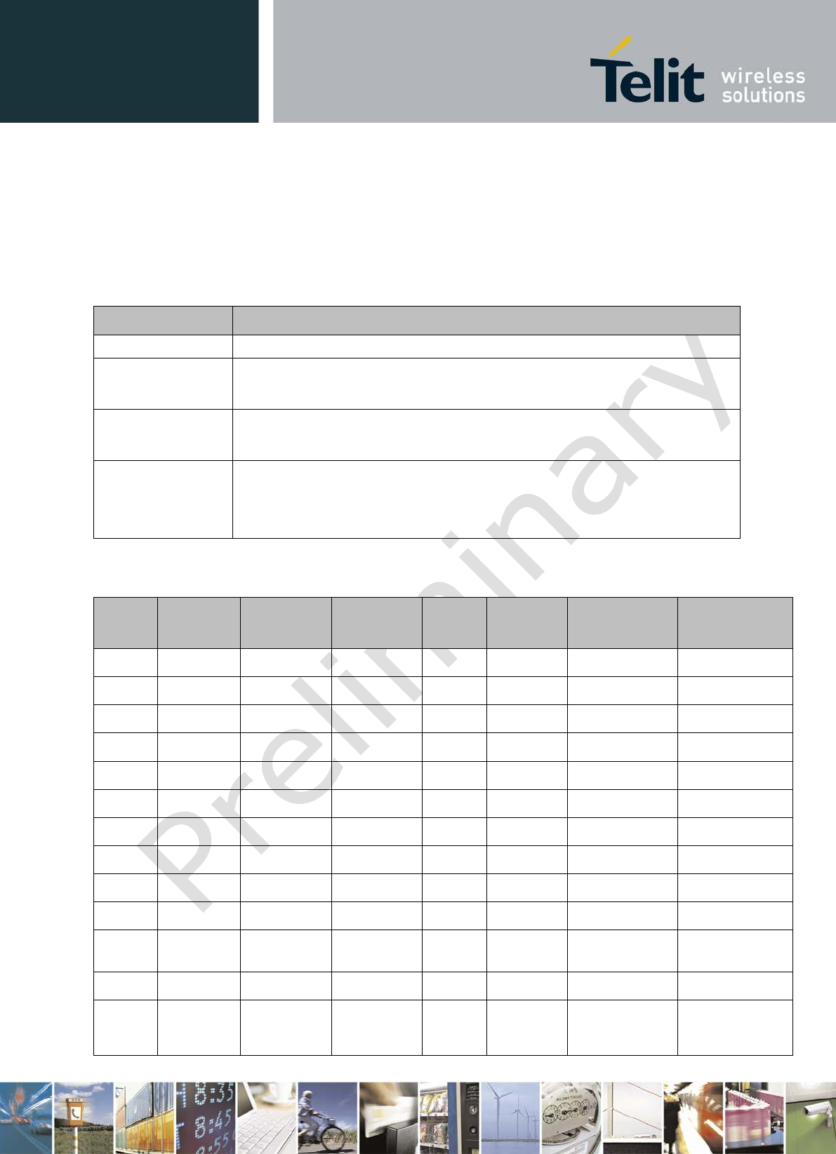
xN930 M.2 Hardware User Guide
1VV0301078 Rev.6 – 2013-11-12
9.7 Antenna Recommendations
The following tables provide antenna guidance for the platform designer.
Ta ble 3 1 Antenna Recommendation
Parameter Recommendation
Impedance
50 ohm
Antenna Shape
and Radiation
Pattern
Near Omni-directional in the Horizontal plane is preferred
Polarization
Predominantly vertical polarization and near Omni-Azimuth pattern are
desired;
H-polarization must not be eliminated ( indoor, diversity)
Input Power
32 dBm typical peak power GSM LB
29.5 dBm typical peak power GSM HB
23.5 dBm typical average power WCDMA
23 dBm typical average power LTE
Ta ble 3 2 Ant e nna Recom m e nda t ion - Ba n dw idt h of M a in & D iver sit y Ant enna
RF
Band
Center
Frequency
Uplink (UL)
UE Tx
Downlink
(DL) UE Rx
Duplex
Mode
Common
Name
Bandwidth of
Main Antenna
(MHz)
Bandwidth of
Diversity Antenna
(MHz)
001 I (1) 2100 MHz
1920 MHz to
1980 MHz
2110 MHz to
2170 MHz
FDD IMT 250 60
002 II (2) 1900 MHz
1850 MHz to
1910 MHz
1930 MHz to
1990 MHz
FDD PCS 140 60
003 III (3) 1800 MHz
1710 MHz to
1785 MHz
1805 MHz to
1880 MHz
FDD DCS 170 75
004 IV (4) 1700 MHz
1710 MHz to
1755 MHz
2110 MHz to
2155 MHz
FDD AWS 445 45
005 V (5) 850 MHz
824 MHz to
849 MHz
869 MHz to
894 MHz
FDD CLR 70 25
006 VI (6) 850 MHz
830 MHz to
840 MHz
875 MHz to
885 MHz
FDD UMTS 800 55 10
007 VII (7) 2600 MHz
2500 MHz to
2570 MHz
2620 MHz to
2690 MHz
FDD IMT-E 190 70
008 VIII
(8)
900 MHz
880 MHz to
915 MHz
925 MHz to
960 MHz
FDD GSM 80 35
009 IX (9) 1800 MHz
1749.9 MHz to
1784.9 MHz
1844.9 MHz to
1879.9 MHz
FDD UMTS 1800 130 35
010 X (10) 1700 MHz
1710 MHz to
1770 MHz
2110 MHz to
2170 MHz
FDD
Extended
AWS
460 60
011 XI
(11) 1500 MHz 1427.9 MHz to
1447.9 MHz
1475.9 MHz
to
1495.9 MHz
FDD PDC 68 20
013 XIII
(13)
750 MHz
777 MHz to
787 MHz
746 MHz to
756 MHz
FDD
upper SMH
block C
41 10
017 XVII
(17) 700 MHz
704 MHz
to
716 MHz
734 MHz
to
746 MHz
FDD
lower SMH
blocks B/C
(subset of
band 12)
42 12
Reproduction forbidden without written authorization from Telit Communications S.p.A. - All Rights Reserved. Page 62 of 77
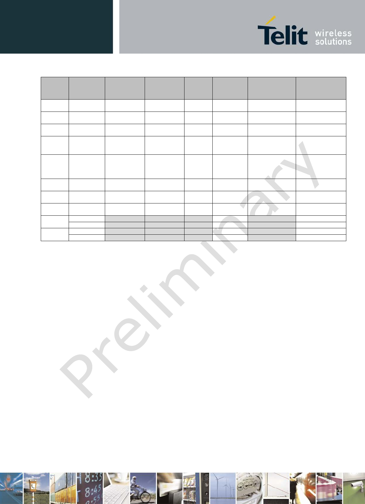
xN930 M.2 Hardware User Guide
1VV0301078 Rev.6 – 2013-11-12
RF
Band
Center
Frequency
Uplink (UL)
UE Tx
Downlink
(DL) UE Rx
Duplex
Mode
Common
Name
Bandwidth of
Main Antenna
(MHz)
Bandwidth of
Diversity Antenna
(MHz)
018 XVIII
(18)
850 MHz
815 MHz to
830 MHz
860 MHz to
875 MHz
FDD
Japan lower
800
60 15
019 XIX
(19)
850 MHz
830 MHz to
845 MHz
875 MHz to
890 MHz
FDD
Japan upper
800
60 15
020 XX
(20)
800 MHz
832 MHz to
862 MHz
791 MHz to
821 MHz
FDD
EU's Digital
Dividend
71 30
021 XXI
(21) 1500 MHz 1447.9 MHz to
1462.9 MHz
1495.9 MHz
to
1510.9 MHz
FDD PDC 63 15.4
025 XXV
(25) 1900 MHz 1850 MHz to
1915 MHz
1930 MHz to
1995 MHz FDD
Extended
PCS
(superset of
band 2)
145 65
026 XXVI
(26)
850MHz
814 MHz to
849 MHz
859 MHz to
894 MHz
FDD ESM+CLR 80 35
027 XXVII
(27)
850MHz
806 MHz to
824 MHz
851 MHz to
869 MHz
FDD ESMR 63 18
028 XXVIII
(28)
750MHz
703 MHz to 728
MHz
758 MHz to
803 MHz
FDD APAC 700 100 45
GPS
1575.42 MHz
GPS L1
35
1227.6 MHz
GPS L2
35
GLONASS
1602 MHz
GLONASS L1
35
1246 MHz
GLONASS L2
35
Reproduction forbidden without written authorization from Telit Communications S.p.A. - All Rights Reserved. Page 63 of 77
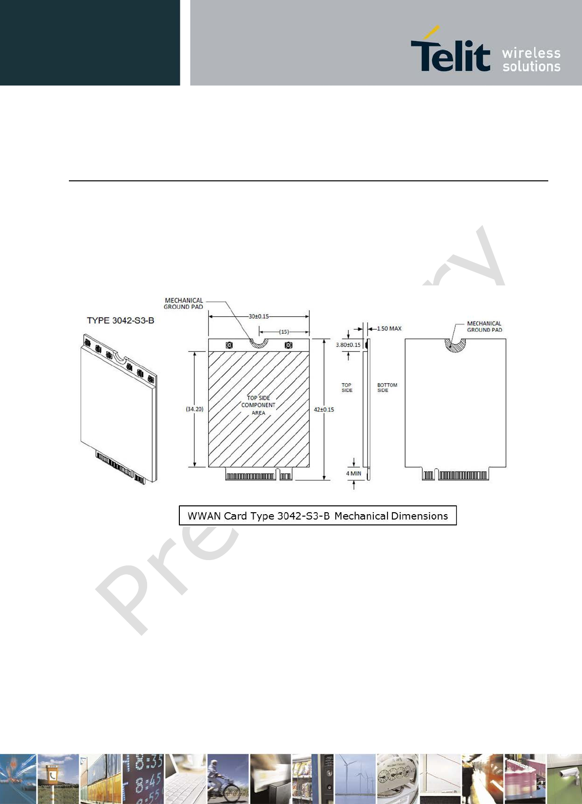
xN930 M.2 Hardware User Guide
1VV0301078 Rev.6 – 2013-11-12
10 WWAN Card Type 3042-S3-B
10.1 Mechanical Dimensions
The mechanical dimensions of WWAN Card Type 3042 are shown in
Figure 14.
The WWAN card is 30 mm x 42 mm. The height is 1.5 mm from the top of the PCB to the
top of the outside shield. There are a total of 75 pins; however 8 pins are lost to support the
slot+. All components are mounted on the Top side.
Figur e 1 4 W W AN Ca rd 3 0 4 2 M echa nica l Dim e nsion s
Reproduction forbidden without written authorization from Telit Communications S.p.A. - All Rights Reserved. Page 64 of 77
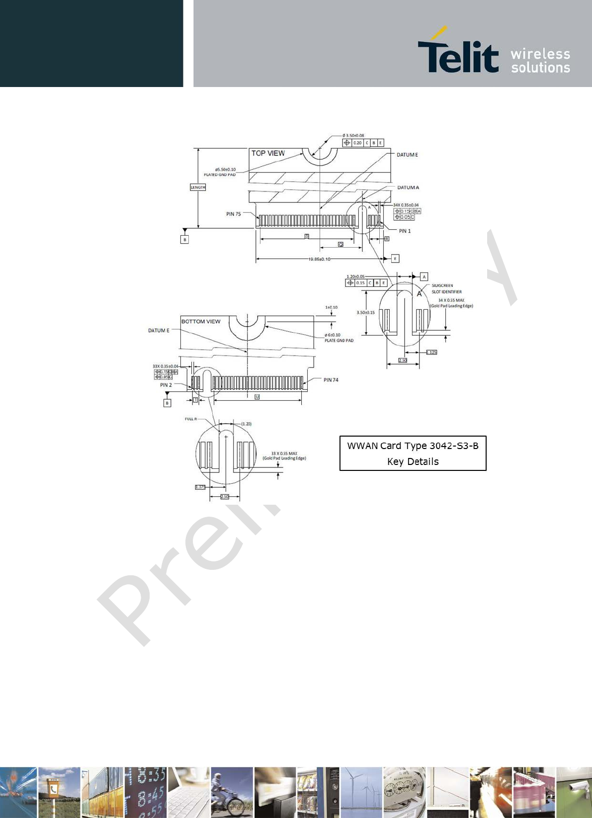
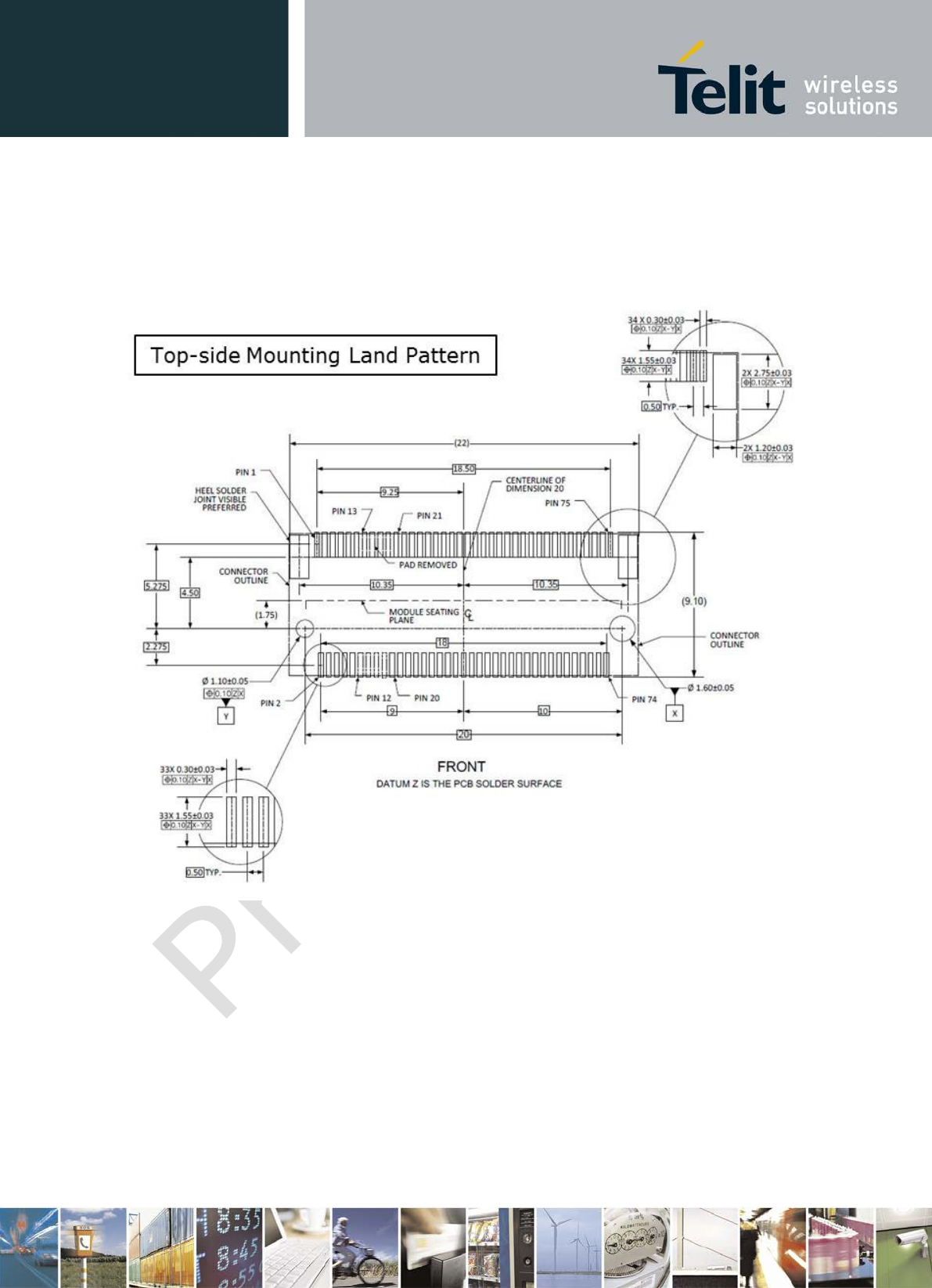
xN930 M.2 Hardware User Guide
1VV0301078 Rev.6 – 2013-11-12
10.2 Land Pattern
Figure 16 illustrates a typical land pattern for a top-mount connector with the key removed.
Figur e 1 6 W W AN Ca rd Type 3 0 4 2 Top-Side M ou nt ing La nd Pa t t er n
Reproduction forbidden without written authorization from Telit Communications S.p.A. - All Rights Reserved. Page 66 of 77
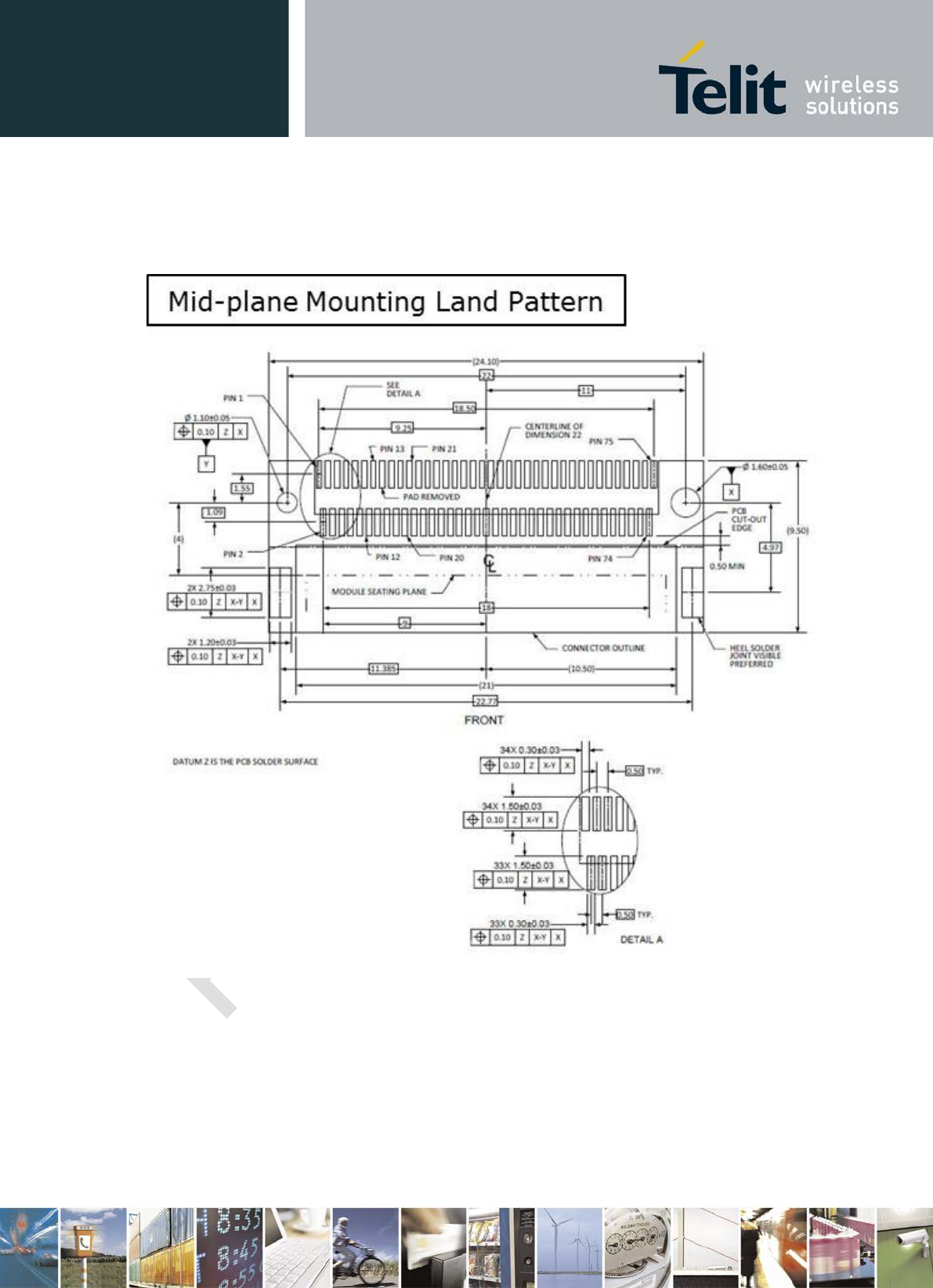
xN930 M.2 Hardware User Guide
1VV0301078 Rev.6 – 2013-11-12
Figure 17 illustrates a typical mid-plane (in-line) land pattern with key removed.
Figur e 1 7 W W AN Ca rd 3 0 4 2 M id-pla ne La n d Pat ter n w it h Key Rem oved
Reproduction forbidden without written authorization from Telit Communications S.p.A. - All Rights Reserved. Page 67 of 77

xN930 M.2 Hardware User Guide
1VV0301078 Rev.6 – 2013-11-12
10.3 Antenna Connector Locations
Figure 18 illustrates the locations for the mina Rx/Tx antenna and the Diversity/GPS antenna.
Antenna locations are still under review.
Figur e 1 8 Ant e nna Conne ct or Loca t ion
ANT1: Diversity/ GPS Antenna
ANT4: Main Antenna
Reproduction forbidden without written authorization from Telit Communications S.p.A. - All Rights Reserved. Page 68 of 77
xN930 M.2 Hardware User Guide
1VV0301078 Rev.6 – 2013-11-12
11 Safety Recommendations
READ CAREFULLY
Be sure the use of this product is allowed in the country and in the environment required. The
use of this product may be dangerous and has to be avoided in the following areas:
• Where it can interfere with other electronic devices in environments such as hospitals,
airports, aircrafts, etc.
• Where there is risk of explosion such as gasoline stations, oil refineries, etc. It is
responsibility of the user to enforce the country regulation and the specific
environment regulation.
Do not disassemble the product; any mark of tampering will compromise the warranty
validity. We recommend following the instructions of the hardware user guides for a correct
wiring of the product. The product has to be supplied with a stabilized voltage source and the
wiring has to be conforming to the security and fire prevention regulations. The product has to
be handled with care, avoiding any contact with the pins because electrostatic discharges may
damage the product itself. Same cautions have to be taken for the SIM, checking carefully the
instruction for its use. Do not insert or remove the SIM when the product is in power saving
mode.
The system integrator is responsible of the functioning of the final product; therefore, care has
to be taken to the external components of the module, as well as of any project or installation
issue, because the risk of disturbing the GSM network or external devices or having impact
on the security. Should there be any doubt, please refer to the technical documentation and the
regulations in force. Every module has to be equipped with a proper antenna with specific
characteristics. The antenna has
to be installed with care in order to avoid any interference with other electronic devices and
has to guarantee a minimum distance from the body (20 cm). In case of this requirement
cannot be satisfied, the system integrator has to assess the final product against the SAR
regulation.
The European Community provides some Directives for the electronic equipments
introduced on the market. All the relevant information’s are available on the European
Community website:
http://ec.europa.eu/enterprise/sectors/rtte/documents/
The text of the Directive 99/05 regarding telecommunication equipments is available,
while the applicable Directives (Low Voltage and EMC) are available at:
http://ec.europa.eu/enterprise/sectors/electrical/
Reproduction forbidden without written authorization from Telit Communications S.p.A. - All Rights Reserved. Page 69 of 77

xN930 M.2 Hardware User Guide
1VV0301078 Rev.6 – 2013-11-12
12 Conformity assessment issues
The following chapters are related to the M.2 module on the EVK carrier board.
12.1 1999/5/EC Directive
The xN930 products portfolio has been evaluated against the essential requirements of the
1999/5/EC Directive.
Bulgarian
С настоящето Telit Communications S.p.A. декларира, че 2G/3G module отговаря на
съществените изисквания и другите приложими изисквания на Директива 1999/5/ЕС.
Czech
Telit Communications S.p.A. tímto prohlašuje, že tento 2G/3G module je ve shodě se základními
požadavky a dalšími příslušnými ustanoveními směrnice 1999/5/ES.
Danish
Undertegnede Telit Communications S.p.A. erklærer herved, at følgende udstyr 2G/3G module
overholder de væsentlige krav og øvrige relevante krav i direktiv 1999/5/EF.
Dutch
Hierbij verklaart Telit Communications S.p.A. dat het toestel 2G/3G module in
overeenstemming is met de essentiële eisen en de andere relevante bepalingen van richtlijn
1999/5/EG.
English
Hereby, Telit Communications S.p.A., declares that this 2G/3G module is in compliance with
the essential requirements and other relevant provisions of Directive 1999/5/EC.
Estonian
Käesolevaga kinnitab Telit Communications S.p.A. seadme 2G/3G module vastavust direktiivi
1999/5/EÜ põhinõuetele ja nimetatud direktiivist tulenevatele teistele asjakohastele sätetele.
German
Hiermit erklärt Telit Communications S.p.A., dass sich das Gerät 2G/3G module in
Übereinstimmung mit den grundlegenden Anforderungen und den übrigen einschlägigen
Bestimmungen der Richtlinie 1999/5/EG befindet.
Greek
ΜΕ ΤΗΝ ΠΑΡΟΥΣΑ Telit Communications S.p.A. ΔΗΛΩΝΕΙ ΟΤΙ 2G/3G module
ΣΥΜΜΟΡΦΩΝΕΤΑΙ ΠΡΟΣ ΤΙΣ ΟΥΣΙΩΔΕΙΣ ΑΠΑΙΤΗΣΕΙΣ ΚΑΙ ΤΙΣ ΛΟΙΠΕΣ ΣΧΕΤΙΚΕΣ
ΔΙΑΤΑΞΕΙΣ ΤΗΣ ΟΔΗΓΙΑΣ 1999/5/ΕΚ.
Hungarian
Alulírott, Telit Communications S.p.A. nyilatkozom, hogy a 2G/3G module megfelel a
vonatkozó alapvetõ követelményeknek és az 1999/5/EC irányelv egyéb elõírásainak.
Finnish
Telit Communications S.p.A. vakuuttaa täten että 2G/3G module tyyppinen laite on direktiivin
1999/5/EY oleellisten vaatimusten ja sitä koskevien direktiivin muiden ehtojen mukainen.
French
Par la présente Telit Communications S.p.A. déclare que l'appareil 2G/3G module est conforme
aux exigences essentielles et aux autres dispositions pertinentes de la directive 1999/5/CE.
Icelandic
Hér með lýsir Telit Communications S.p.A. yfir því að 2G/3G module er í samræmi við
grunnkröfur og aðrar kröfur, sem gerðar eru í tilskipun 1999/5/EC
Italian
Con la presente Telit Communications S.p.A. dichiara che questo 2G/3G module è conforme ai
requisiti essenziali ed alle altre disposizioni pertinenti stabilite dalla direttiva 1999/5/CE.
Latvian
Ar šo Telit Communications S.p.A. deklarē, ka 2G/3G module atbilst Direktīvas 1999/5/EK
būtiskajām prasībām un citiem ar to saistītajiem noteikumiem.
Lithuanian
Šiuo Telit Communications S.p.A. deklaruoja, kad šis 2G/3G module atitinka esminius
reikalavimus ir kitas 1999/5/EB Direktyvos nuostatas.
Maltese
Hawnhekk, Telit Communications S.p.A., jiddikjara li dan 2G/3G module jikkonforma mal-
ħtiġijiet essenzjali u ma provvedimenti oħrajn relevanti li hemm fid-Dirrettiva 1999/5/EC.
Reproduction forbidden without written authorization from Telit Communications S.p.A. - All Rights Reserved. Page 70 of 77

xN930 M.2 Hardware User Guide
1VV0301078 Rev.6 – 2013-11-12
Norwegian
Telit Communications S.p.A. erklærer herved at utstyret 2G/3G module er i samsvar med de
grunnleggende krav og øvrige relevante krav i direktiv 1999/5/EF.
Polish
Niniejszym Telit Communications S.p.A. oświadcza, że 2G/3G module jest zgodny z
zasadniczymi wymogami oraz pozostałymi stosownymi postanowieniami Dyrektywy 1999/5/EC
Portuguese
Telit Communications S.p.A. declara que este 2G/3G module está conforme com os requisitos
essenciais e outras disposições da Directiva 1999/5/CE.
Slovak
Telit Communications S.p.A. týmto vyhlasuje, že 2G/3G module spĺňa základné požiadavky a
všetky príslušné ustanovenia Smernice 1999/5/ES.
Slovenian
Telit Communications S.p.A. izjavlja, da je ta 2G/3G modul v skladu z bistvenimi zahtevami in
ostalimi relevantnimi določili direktive 1999/5/ES.
Spanish
Por medio de la presente Telit Communications S.p.A. declara que el 2G/3G module cumple con
los requisitos esenciales y cualesquiera otras disposiciones aplicables o exigibles de la Directiva
1999/5/CE.
Swedish
Härmed intygar Telit Communications S.p.A. att denna 2G/3G module står I överensstämmelse
med de väsentliga egenskapskrav och övriga relevanta bestämmelser som framgår av direktiv
1999/5/EG.
In order to satisfy the essential requirements of 1999/5/EC Directive, the xN930 is
compliant with the following standards:
RF spectrum use (R&TTE art. 3.2) EN 300 440-2 V1.4.1
EN 301 511 V9.0.2
EN 301 908-1 V6.2.1
EN 301 908-2 V5.2.1
EN 301 908-13 V5.2.1
EN 300 440-1 V1.6.1
EMC (R&TTE art. 3.1b) EN 301 489-1 V1.9.2
EN 301 489-3 V1.4.1
EN 301 489-7 V1.3.1
EN 301 489-24 V1.5.1
Health & Safety (R&TTE art. 3.1a) EN 60950-1:2006 + A11:2009 + A1:2010 + A12:2011
EN 62311: 2008
Reproduction forbidden without written authorization from Telit Communications S.p.A. - All Rights Reserved. Page 71 of 77
xN930 M.2 Hardware User Guide
1VV0301078 Rev.6 – 2013-11-12
The conformity assessment procedure referred to in Article 10 and detailed in Annex IV of
Directive 1999/5/EC has been followed with the involvement of the following Notified
Body:
Thus, the following marking is included in the product:
The full declaration of conformity can be found on the following address:
http://www.telit.com/
There is no restriction for the commercialization in all the countries of the European Union.
Final product integrating this module must be assessed against essential requirements of
the 1999/5/EC (R&TTE) Directive. It should be noted that assessment does not necessarily
lead to testing. Telit Communications S.p.A. recommends carrying out the following
assessments:
RF spectrum use (R&TTE art.
3.2)
It will depend on the antenna used on the final
product.
EMC (R&TTE art. 3.1b) Testing
Health & Safety (R&TTE art.
3.1a)
Testing
Alternately, assessment of the final product against EMC (Art. 3.1b) and Electrical safety
(Art. 3.1a) essential requirements can be done against the essential requirements of the
EMC and the LVD Directives:
• Low Voltage Directive 2006/95/EC and product safety
• Directive EMC 2004/108/EC for conformity for EMC
12.2 CE RF Exposure Compliance
This device meets the EU requirements (1999/519/EC) and the International Commission on
Non-Ionizing Radiation Protection (ICNIRP) on the limitation of exposure of the general
public to electromagnetic fields by way of health protection.
To comply with the RF exposure requirements, this module must be installed in a host
platform that is intended to be operated in a minimum of 20 cm separation distance to the user.
Reproduction forbidden without written authorization from Telit Communications S.p.A. - All Rights Reserved. Page 72 of 77

xN930 M.2 Hardware User Guide
1VV0301078 Rev.6 – 2013-11-12
12.3 R&TTE Regulation:
In all cases assessment of the final product must be met against the Essential requirements of
the R&TTE Directive Articles 3.1(a) and (b), safety and EMC respectively, as well as any
relevant Article 3.3 requirements.
1. The Dipole antenna (gain: GPRS/EGPRS/WCDMA/LTE: 2dBi) was verified in the
conformity testing, and for compliance the antenna shall not be modified. A separate approval
is required for all other operating configurations, including different antenna configurations.
2. If any other simultaneous transmission radio is installed in the host platform together with
this module, or above restrictions cannot be kept, a separate RF exposure assessment and CE
equipment certification is required.
Reproduction forbidden without written authorization from Telit Communications S.p.A. - All Rights Reserved. Page 73 of 77

xN930 M.2 Hardware User Guide
1VV0301078 Rev.6 – 2013-11-12
13 FCC/IC Regulatory notices
13.1 Modification statement
Telit has not approved any changes or modifications to this device by the user. Any changes
or modifications could void the user’s authority to operate the equipment.
Telit n’approuve aucune modification apportée à l’appareil par l’utilisateur, quelle qu’en soit
la nature. Tout changement ou modification peuvent annuler le droit d’utilisation de
l’appareil par l’utilisateur.
13.2 Interference statement
This device complies with Part 15 of the FCC Rules and Industry Canada licence-exempt
RSS standard(s). Operation is subject to the following two conditions: (1) this device may not
cause interference, and (2) this device must accept any interference, including interference
that may cause undesired operation of the device.
Le présent appareil est conforme aux CNR d'Industrie Canada applicables aux appareils
radio exempts de licence. L'exploitation est autorisée aux deux conditions suivantes : (1)
l'appareil ne doit pas produire de brouillage, et (2) l'utilisateur de l'appareil doit accepter
tout brouillage radioélectrique subi, même si le brouillage est susceptible d'en compromettre
le fonctionnement.
13.3 FCC Class B digital device notice
This equipment has been tested and found to comply with the limits for a Class B digital device, pursuant to part
15 of the FCC Rules. These limits are designed to provide reasonable protection against harmful interference in a
residential installation. This equipment generates, uses and can radiate radio frequency energy and, if not installed
and used in accordance with the instructions, may cause harmful interference to radio communications. However,
there is no guarantee that interference will not occur in a particular installation. If this equipment does cause
harmful interference to radio or television reception, which can be determined by turning the equipment off and on,
the user is encouraged to try to correct the interference by one or more of the following measures:
- Reorient or relocate the receiving antenna.
- Increase the separation between the equipment and receiver.
- Connect the equipment into an outlet on a circuit different from that to which the receiver
is connected.
- Consult the dealer or an experienced radio/TV technician for help.
Reproduction forbidden without written authorization from Telit Communications S.p.A. - All Rights Reserved. Page 74 of 77

xN930 M.2 Hardware User Guide
1VV0301078 Rev.6 – 2013-11-12
13.4 Radiation Exposure Statement
This equipment complies with FCC radiation exposure limits set forth for an uncontrolled
environment. This equipment should be installed and operated with minimum distance 20 cm
between the radiator & your body.
13.5 End Product Labeling
When the module is installed in the host device, the FCC ID label must be visible through a
window on the final device or it must be visible when an access panel, door or cover is easily
re-moved. If not, a second label must be placed on the outside of the final device that contains
the following text: “Contains FCC ID: RI7LN930”. The grantee's FCC ID can be used only
when all FCC compliance requirements are met.
This device is intended only for OEM integrators under the following conditions:
(1) The antenna must be installed such that 20 cm is maintained between the antenna and users,
(2) The transmitter module may not be co-located with any other transmitter or antenna.
(3) To comply with FCC regulations limiting both maximum RF output power and human
exposure to RF radiation, the maximum antenna gain including cable loss in a mobile exposure
condition must not exceed:
。 5.0 dBi in Cellular band
。 3.0 dBi in PCS band
。 5.5 dBi in AWS band
。 5.0 dBi in 700 MHz band
。 5.0 dBi in 2500MHz band
In the event that these conditions cannot be met (for example certain laptop configurations or
co-location with another transmitter), then the FCC authorization is no longer considered valid
and the FCC ID cannot be used on the final product. In these circumstances, the OEM
integrator will be responsible for re-evaluating the end product (including the transmitter) and
obtaining a separate FCC authorization.
Reproduction forbidden without written authorization from Telit Communications S.p.A. - All Rights Reserved. Page 75 of 77
xN930 M.2 Hardware User Guide
1VV0301078 Rev.6 – 2013-11-12
14 Document History
Revision
Date
Changes
0
2013-05-20
First issue
1
2013-07-09
• Update setting for Pin 21 on the host interface. This
signal is not connected.
• Updated pin names of pins 1, 21, 69, and 75 in Table 4
and Table 19 to simply reflect HW Configuration use.
• Updated Table 24 to indicate configuration pins 1, 69,
and 75 are tied to GND.
• Rename section 3.6 Coexistence Interface to In-Device
Coexistence Interface. Additional information on the Inter-
device coexistence support was added.
• Updated section 4.1.3 System Trace Tool Section.
• Updated Figure 5 – RF Engine for WW SKU.
• Add further information USB LPM to USB section
• Added information on Seamless Roaming & Wifi Off-
load – SIM_EAP, SIM-AKA under Other Requirements
• Added information on Antenna Design Guidelines
under Other Requirements.
2
2013-07-29
RF bands updated
3
2013-08-26
Updating on RF bands
Updated section 3.5 and 3.4.5
Updated temp range
4
2013-09-09
HN930-DC product was removed from portfolio
5
2013-09-15
Main & Diversity antenna positions have been swapped.
• Updated documentation accordingly, Figure 6 and
Figure 10.
• Updated WWAN M.2 Mechanical drawings, Figure 14
through Figure 17.
• Updated Card_power_ON_OFF description for
UltraBook in Table 9.
• Updated comments in Table 15 regarding the
DPR#/SAR signal.
• Updated SIM DTECTED signal to indicate an external
pull-up.
• Updated Platform Block Diagrams to show DPR#
signal is connected to an EINT pin (not GPIO) on
XGOLD.
• Identified Audio Signals on host interface in Table 4.
Previously these were simply defined as Reserved.
• Updated VBAT requirements in Table 24 and Table
25.
Reproduction forbidden without written authorization from Telit Communications S.p.A. - All Rights Reserved. Page 76 of 77
