Telit Communications S p A UC864AWA GSM 850, E-GSM 900, DCS 1800, PCS 1900, FDD IV, 2G/3.5G module User Manual Users guide
Telit Communications S.p.A. GSM 850, E-GSM 900, DCS 1800, PCS 1900, FDD IV, 2G/3.5G module Users guide
Contents
- 1. User guide
- 2. Users guide
Users guide

UC864
-
E
-
AUTO
UC864-AWS-AUTO
Hardware User Guide
1vv0300795 Rev. 11 – 2010/11/18

UC864-E-AUTO / AWS-AUTO Hardware User Guide
1vv0300795 Rev.11 – 2010/11/18
Reproduction forbidden without Telit Communications S.p.A’s. written authorization - All Rights Reserved. Page 2 of 78
This document is relating to the following products:
PRODUCT
UC864-E-AUTO
UC864-AWS-AUTO

UC864-E-AUTO / AWS-AUTO Hardware User Guide
1vv0300795 Rev.11 – 2010/11/18
Reproduction forbidden without Telit Communications S.p.A’s. written authorization - All Rights Reserved. Page 3 of 78
Disclaimer
The information contained in this document is the proprietary information of Telit
Communications S.p.A. and its affiliates (“TELIT”). The contents are confidential and
any disclosure to persons other than the officers, employees, agents or
subcontractors of the owner or licensee of this document, without the prior written
consent of Telit, is strictly prohibited.
Telit makes every effort to ensure the quality of the information it makes available.
Notwithstanding the foregoing, Telit does not make any warranty as to the
information contained herein, and does not accept any liability for any injury, loss or
damage of any kind incurred by use of or reliance upon the information.
Telit disclaims any and all responsibility for the application of the devices
characterized in this document, and notes that the application of the device must
comply with the safety standards of the applicable country, and where applicable,
with the relevant wiring rules.
Telit reserves the right to make modifications, additions and deletions to this
document due to typographical errors, inaccurate information, or improvements to
programs and/or equipment at any time and without notice. Such changes will,
nevertheless be incorporated into new editions of this application note.
All rights reserved.
© 2008, 2010 Telit Communications S.p.A.

UC864-E-AUTO / AWS-AUTO Hardware User Guide
1vv0300795 Rev.11 – 2010/11/18
Reproduction forbidden without Telit Communications S.p.A’s. written authorization - All Rights Reserved. Page 4 of 78
Contents
1.
OVERVIEW ............................................................................................................................................................... 6
2.
MECHANICAL DIMENSIONS ............................................................................................................................... 7
2.1.
UC864-E-AUTO
/
AWS-AUTO
M
ECHANICAL
D
IMENSIONS
................................................................................. 7
3.
UC864-E-AUTO / AWS-AUTO MODULE CONNECTIONS............................................................................... 8
3.1.
PIN-OUT ............................................................................................................................................................. 8
4.
TEMPERATURE RANGE ..................................................................................................................................... 12
4.1.
A
NTENNA
C
ONNECTOR
(
S
) ................................................................................................................................... 13
5.
HARDWARE COMMANDS .................................................................................................................................. 14
5.1.
T
URNING
ON
THE
UC864-E-AUTO
/
AWS-AUTO ............................................................................................. 14
5.2.
I
NITIALIZATION AND
A
CTIVATION STATE
................................................................................................................ 15
5.3.
T
URNING
OFF
THE
UC864-E-AUTO
/
AWS-AUTO ........................................................................................... 17
5.3.1.
Shutdown by Software Command
........................................................................................................ 18
5.3.2.
Hardware Shutdown
.............................................................................................................................. 19
5.3.3.
Hardware Unconditional Restart
......................................................................................................... 20
5.4.
S
UMMARY OF
T
URNING
ON
AND
OFF
THE MODULE
.............................................................................................. 21
6.
POWER SUPPLY .................................................................................................................................................... 22
6.1.
P
OWER
S
UPPLY
R
EQUIREMENTS
.......................................................................................................................... 22
6.2.
G
ENERAL
D
ESIGN
R
ULES
.................................................................................................................................... 24
6.2.1.
Electrical Design Guidelines
................................................................................................................ 24
6.2.2.
Thermal Design Guidelines
.................................................................................................................. 30
6.2.3.
Power Supply PCB Layout Guidelines
................................................................................................. 32
7.
ANTENNA(S) ........................................................................................................................................................... 34
7.1.
GSM/WCDMA
A
NTENNA
R
EQUIREMENTS
.......................................................................................................... 34
7.2.
GSM/WCDMA
A
NTENNA
-
I
NSTALLATION
G
UIDELINES
....................................................................................... 35
8.
LOGIC LEVEL SPECIFICATIONS ..................................................................................................................... 36
8.1.
R
ESET
S
IGNAL
.................................................................................................................................................... 37
9.
USB PORT................................................................................................................................................................ 38
9.1.
USB
TRANSCEIVER SPECIFICATIONS
.................................................................................................................... 39
10.
SERIAL PORTS .................................................................................................................................................. 40
10.1.
M
ODEM
S
ERIAL
P
ORT
.......................................................................................................................................... 40
10.2.
RS232
L
EVEL
T
RANSLATION
............................................................................................................................... 43
10.3.
5V
UART
L
EVEL
T
RANSITION
.............................................................................................................................. 46
11.
AUDIO SECTION OVERVIEW ....................................................................................................................... 48
11.1.
S
ELECTION MODE
................................................................................................................................................ 48
11.2.
E
LECTRICAL
C
HARACTERISTICS
........................................................................................................................... 50
11.2.1.
Input Lines (MIC1 and MIC2) Characteristics
..................................................................................... 50
11.3.
OUTPUT
LINES
(
S
PEAKER
)
.............................................................................................................................. 51

UC864-E-AUTO / AWS-AUTO Hardware User Guide
1vv0300795 Rev.11 – 2010/11/18
Reproduction forbidden without Telit Communications S.p.A’s. written authorization - All Rights Reserved. Page 5 of 78
11.3.1.
Output Lines Characteristics
................................................................................................................ 51
12.
GENERAL PURPOSE I/O ................................................................................................................................. 52
12.1.
L
OGIC
L
EVEL
S
PECIFICATIONS
............................................................................................................................. 54
12.2.
U
SING A
GPIO
P
AD AS
I
NPUT
.............................................................................................................................. 55
12.3.
U
SING A
GPIO
P
AD AS
O
UTPUT
........................................................................................................................... 55
12.4.
U
SING THE
RF
T
RANSMISSION
C
ONTROL
GPIO4 .................................................................................................. 56
12.5.
U
SING THE
RFTXMON
O
UTPUT
GPIO5 .............................................................................................................. 56
12.6.
U
SING THE
A
LARM
O
UTPUT
GPIO6 ..................................................................................................................... 56
12.7.
U
SING THE
B
UZZER
O
UTPUT
GPIO7 .................................................................................................................... 57
12.8.
M
AGNETIC
B
UZZER
C
ONCEPTS
............................................................................................................................ 58
12.8.1.
Short Description
................................................................................................................................... 58
12.8.2.
Frequency Behavior
............................................................................................................................... 59
12.8.3.
Power Supply Influence
........................................................................................................................ 59
12.8.4.
Working Current Influence
................................................................................................................... 59
12.9.
U
SING THE
T
EMPERATURE
M
ONITOR
F
UNCTION
................................................................................................... 60
12.9.1.
Short Description
................................................................................................................................... 60
12.9.2.
Allowed GPIO
.......................................................................................................................................... 60
12.10.
I
NDICATION OF
N
ETWORK
S
ERVICE
A
VAILABILITY
............................................................................................. 62
12.11.
RTC
B
YPASS
O
UT
........................................................................................................................................... 63
12.12.
VAUX1
P
OWER
O
UTPUT
................................................................................................................................. 63
13.
DAC AND ADC SECTION ................................................................................................................................ 64
13.1.
DAC
C
ONVERTER
................................................................................................................................................ 64
13.1.1.
Description
.............................................................................................................................................. 64
13.1.2.
Enabling DAC
.......................................................................................................................................... 64
13.1.3.
Low Pass Filter Example
...................................................................................................................... 65
13.2.
ADC
C
ONVERTER
................................................................................................................................................ 65
13.2.1.
Description
.............................................................................................................................................. 65
13.2.2.
Using ADC Converter
............................................................................................................................. 65
14.
MOUNTING THE MODULE ON YOUR BOARD ......................................................................................... 66
14.1.
A
PPLICATION
PCB
L
AYOUT
................................................................................................................................. 67
14.2.
C
LEARANCE
A
REA
............................................................................................................................................... 69
14.3.
T
HERMAL
D
ISSIPATION
........................................................................................................................................ 69
14.4.
M
ODULE
S
OLDERING
........................................................................................................................................... 70
15.
APPLICATION GUIDE ..................................................................................................................................... 71
15.1.
D
EBUG OF THE
UC864-E-AUTO
/
AWS-AUTO
IN PRODUCTION
......................................................................... 71
15.2.
B
YPASS CAPACITOR ON
P
OWER SUPPLIES
............................................................................................................ 72
15.3.
SIM
INTERFACE
.................................................................................................................................................. 72
15.4.
EMC
RECOMMENDATIONS
................................................................................................................................... 73
16.
PACKING SYSTEM ........................................................................................................................................... 74
17.
CONFORMITY ASSESSMENT ISSUES ......................................................................................................... 75
18.
SAFETY RECOMMENDATIONS .................................................................................................................... 77
19.
DOCUMENT CHANGE LOG ........................................................................................................................... 78

UC864-E-AUTO / AWS-AUTO Hardware User Guide
1vv0300795 Rev.11 – 2010/11/18
Reproduction forbidden without Telit Communications S.p.A’s. written authorization - All Rights Reserved. Page 6 of 78
1. Overview
OverviewOverview
Overview
The aim of this document is the description of some hardware solutions useful for
developing a product with the Telit UC864-E-AUTO and UC864-AWS-AUTO modules.
In this document all the basic functions of a mobile phone will be taken into account;
for each one of them a proper hardware solution will be suggested and eventually the
wrong solutions and common errors to be avoided will be evidenced. Obviously this
document cannot embrace the whole hardware solutions and products that may be
designed. The wrong solutions to be avoided must be considered as mandatory, while
the suggested hardware configurations must not be considered mandatory, instead
the information given must be used as a guide and a starting point for properly
developing your product with the Telit UC864-E-AUTO & UC864-AWS-AUTO modules.
For further hardware details that may not be explained in this document refer to the
Telit UC864-E–AUTO & UC864-AWS-AUTO Product Description document where all
the hardware information is reported.
The information presented in this document is believed to be accurate and reliable. However,
no responsibility is assumed by Telit Communications S.p.A. for its use, nor any infringement
of patents or other rights of third parties which may result from its use. No license is granted
by implication or otherwise under any patent rights of Telit Communications S.p.A. other than
for circuitry embodied in Telit products. This document is subject to change without notice.
NOTICE:
(EN) The integration of the GSM/GPRS/EGPRS/WCDMA/HSDPA UC864-E-AUTO & UC864-
AWS-AUTO cellular module within user application must be done according to the design
rules described in this manual.
(IT) L’integrazione del modulo cellulare GSM/GPRS/EGPRS/WCDMA/HSDPA UC864- E-
AUTO e UC864-AWS-AUTO all’interno dell’applicazione dell’utente dovrà rispettare le
indicazioni progettuali descritte in questo manuale.
(DE) Die Integration des UC864- E-AUTO & UC864-AWS-AUTO
GSM/GPRS/EGPRS/WCDMA/HSDPA Mobilfunk-Moduls in ein Gerät muß gemäß der in
diesem Dokument beschriebenen Kunstruktionsregeln erfolgen
(SL) Integracija GSM/GPRS/EGPRS/WCDMA/HSDPA UC864- E-AUTO & UC864-AWS-
AUTO modula v uporabniški aplikaciji bo morala
upoštevati projektna navodila, opisana v tem
piročniku.
(SP) La utilización del modulo GSM/GPRS/EGPRS/WCDMA/HSDPA UC864- E-AUTO &
UC864-AWS-AUTO debe ser conforme a los usos para los cuales ha sido deseñado
descritos en este manual del usuario.
(FR) L’intégration du module cellulaire GSM/GPRS/EGPRS/WCDMA/HSDPA UC864- E-
AUTO & UC864-AWS-AUTO dans l’application de l’utilisateur sera faite selon les règles de
conception décrites dans ce manuel.
(HE) UC864-
E
-
AUTO
/ AWS
UC864-E-AUTO / AWS-AUTO Hardware User Guide
1vv0300795 Rev.11 – 2010/11/18
Reproduction forbidden without Telit Communications S.p.A’s. written authorization - All Rights Reserved. Page 7 of 78
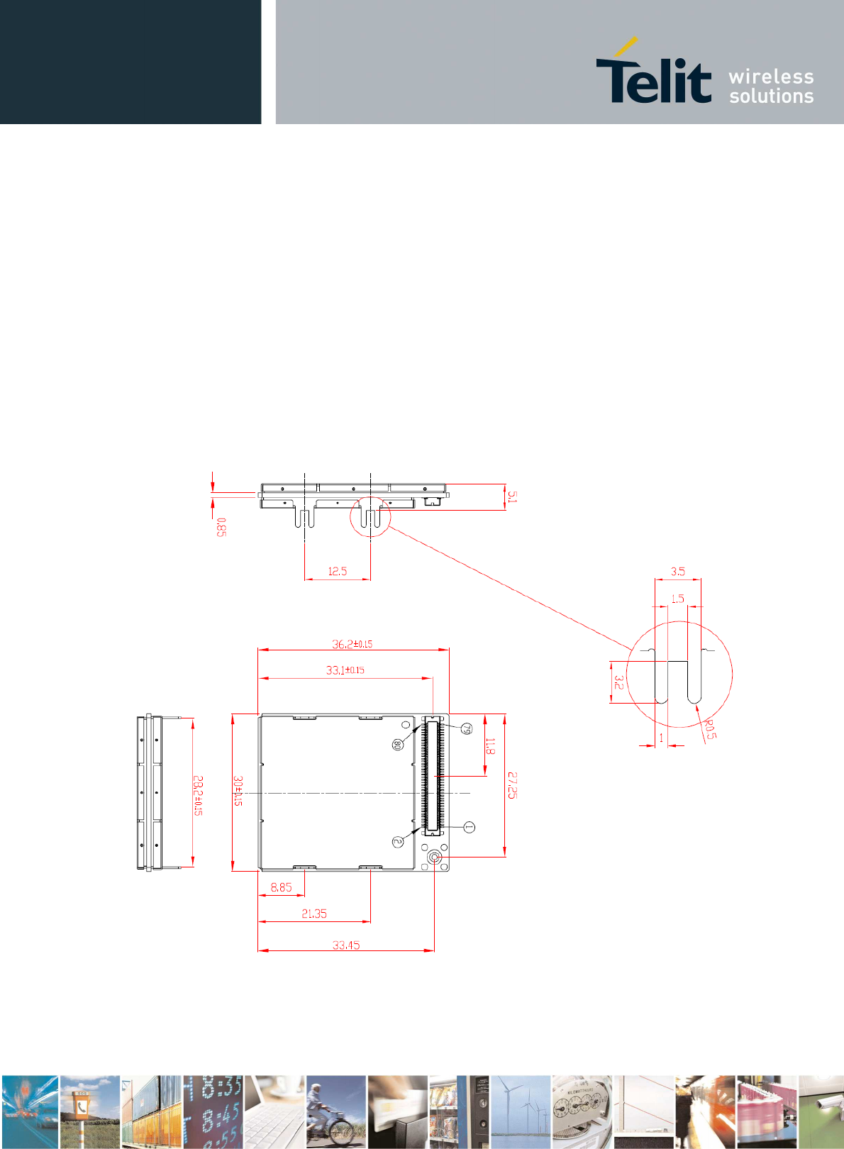
2. Mechanical Dimensions
Mechanical DimensionsMechanical Dimensions
Mechanical Dimensions
2.1. UC864-E-AUTO / AWS-AUTO Mechanical Dimensions
The Telit UC864-E-AUTO / AWS-AUTO module overall dimensions are:
• Length: 36.2 mm
• Width: 30.0 mm
• Thickness: 5.1mm
UC864-E-AUTO / AWS-AUTO Hardware User Guide
1vv0300795 Rev.11 – 2010/11/18
Reproduction forbidden without Telit Communications S.p.A’s. written authorization - All Rights Reserved. Page 8 of 78
3. UC864
UC864UC864
UC864-
--
-E
EE
E-
--
-AUTO
AUTOAUTO
AUTO
/ AWS
/ AWS/ AWS
/ AWS-
--
-AUTO
AUTO AUTO
AUTO M
MM
Module
odule odule
odule C
CC
Connections
onnections onnections
onnections
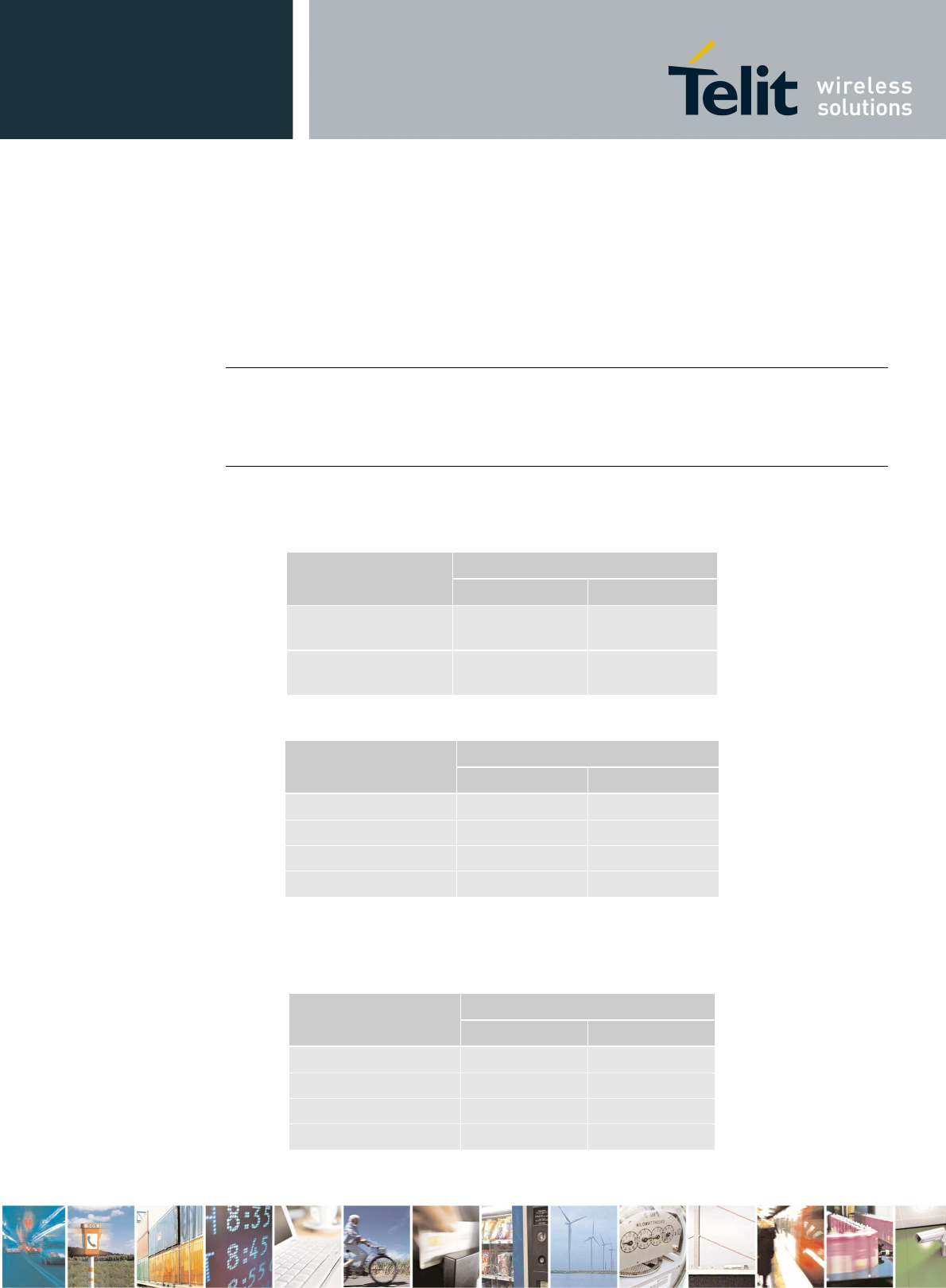
3.1. PIN-OUT
UC864-E-AUTO / AWS-AUTO uses an 80 pin Molex p.n. 53949-0878 male connector
for the connections with the external applications. This connector matches the
54150-0878 models.
Pin
PinPin
Pin
Signal
SignalSignal
Signal
I/O
I/OI/O
I/O
Function
FunctionFunction
Function
Internal
InternalInternal
Internal
Pull up
Pull upPull up
Pull up
Type
TypeType
Type
Power Supply
Power SupplyPower Supply
Power Supply
1
11
1
VBATT -
Main power supply Power
2
22
2
VBATT -
Main power supply Power
3
33
3
VBATT -
Main power supply Power
4
44
4
VBATT -
Main power supply Power
5
55
5
GND -
Ground Power
6
66
6
GND -
Ground Power
7
77
7
GND -
Ground Power
Audio
AudioAudio
Audio
8
88
8
AXE I Hands-free switching CMOS 2.6V
9
99
9
EAR_HF+ AO
Hands-free ear output, phase + Audio
10
1010
10
EAR_HF- AO
Hands-free ear output, phase - Audio
11
1111
11
EAR_MT+ AO
Handset earphone signal output, phase + Audio
12
1212
12
EAR_MT- AO
Handset earphone signal output, phase - Audio
13
1313
13
MIC_HF+ AI
Hands-free microphone input; phase + Audio
14
1414
14
MIC_HF- AI
Hands-free microphone input; phase - Audio
15
1515
15
MIC_MT+ AI
Handset microphone signal input; phase+ Audio
16
1616
16
MIC_MT- AI
Handset microphone signal input; phase- Audio
SIM Card Interface
SIM Card InterfaceSIM Card Interface
SIM Card Interface
18
1818
18
1
11
1
SIMVCC -
External SIM signal – Power supply for the SIM 1.8 / 3V
19
1919
19
SIMRST O
External SIM signal – Reset 1.8 / 3V
20
2020
20
SIMIO I/O
External SIM signal - Data I/O 1.8 / 3V
21
2121
21
SIMIN I External SIM signal - Presence (active low) CMOS 2.6V
22
2222
22
SIMCLK O
External SIM signal – Clock 1.8 / 3V
Trace
TraceTrace
Trace
23
2323
23
RX_TRACE I RX Data for debug monitor CMOS 2.6V
24
2424
24
TX_TRACE O
TX Data for debug monitor CMOS 2.6V
1
On this line a maximum of 10nF bypass capacitor is allowed
UC864-E-AUTO / AWS-AUTO Hardware User Guide
1vv0300795 Rev.11 – 2010/11/18
Reproduction forbidden without Telit Communications S.p.A’s. written authorization - All Rights Reserved. Page 9 of 78
Pin
PinPin
Pin
Signal
SignalSignal
Signal
I/O
I/OI/O
I/O
Function
FunctionFunction
Function
Internal
InternalInternal
Internal
Pull up
Pull upPull up
Pull up
Type
TypeType
Type
Prog. / Data + Hw Flow Control
Prog. / Data + Hw Flow ControlProg. / Data + Hw Flow Control
Prog. / Data + Hw Flow Control
25
2525
25
C103/TXD I Serial data input (TXD) from DTE Pull-Down CMOS 2.6V
26
2626
26
C104/RXD O
Serial data output to DTE Pull-Up CMOS 2.6V
27
2727
27
C107/DSR O
Output for Data set ready signal (DSR) to DTE Pull-Down CMOS 2.6V
28
2828
28
C106/CTS O
Output for Clear to send signal (CTS) to DTE Pull-Up CMOS 2.6V
29
2929
29
C108/DTR I Input for Data terminal ready signal (DTR) from DTE Pull-Up CMOS 2.6V
30
3030
30
C125/RING O
Output for Ring indicator signal (RI) to DTE Pull-Up CMOS 2.6V
31
3131
31
C105/RTS I Input for Request to send signal (RTS) from DTE Pull-Down CMOS 2.6V
32
3232
32
C109/DCD O
Output for Data carrier detect signal (DCD) to DTE Pull-Up CMOS 2.6V
Miscellaneous Functions
Miscellaneous FunctionsMiscellaneous Functions
Miscellaneous Functions
35
3535
35
USB_ID AI
Analog input used to sense whether a
peripheral device is connected, and
determine the peripheral type, a host
or a peripheral
Analog
36
3636
36
PCM_CLOCK I/O
PCM clock out Pull-Down
CMOS 2.6V
DAC and ADC
DAC and ADCDAC and ADC
DAC and ADC
37
3737
37
ADC_IN1 AI
Analog/Digital converter input A/D
38
3838
38
ADC_IN2 AI
Analog/Digital converter input A/D
39
3939
39
ADC_IN3 AI
Analog/Digital converter input A/D
40
4040
40
DAC_OUT AO
Digital/Analog converter output D/A
Miscellaneous Functions
Miscellaneous FunctionsMiscellaneous Functions
Miscellaneous Functions
45
4545
45
STAT_LED O
Status indicator led CMOS 1.8V
46
4646
46
GND -
Ground Ground
48
4848
48
USB_VBUS
AI
/A
O
Power supply for the internal USB transceiver. This pin is
configured as an analog input or an analog output depending
upon the type of peripheral device connected.
47K
Ω
pull-down
4.4V ~5.25V
49
4949
49
PWRMON O
Power ON Monitor 1K
Ω
CMOS 2.6V
50
5050
50
VAUX1 -
Power output for external accessories
51
5151
51
CHARGE AI
Charger input 10K
Ω
pull-down
Power
52
5252
52
CHARGE AI
Charger input Power
53
5353
53
ON/OFF I
Input command for switching power ON or OFF (toggle
command).
Pulled up on
chip
54
5454
54
RESET I Reset input 10K
Ω
55
5555
55
VRTC AO
Power supply for RTC block Power
Telit GPIOs
Telit GPIOsTelit GPIOs
Telit GPIOs
56
5656
56
GPIO_19 I/O
GPIO19 Configurable GPIO CMOS 2.6V
57
5757
57
GPIO_11 I/O
GPIO11 Configurable GPIO CMOS 2.6V
58
5858
58
GPIO_20 I/O
GPIO20 Configurable GPIO CMOS 2.6V
59
5959
59
GPIO_04 I/O
GPIO4 Configurable GPIO CMOS 2.6V
60
6060
60
GPIO_14 I/O
GPIO14 Configurable GPIO CMOS 2.6V
61
6161
61
GPIO_15 I/O
GPIO15 Configurable GPIO CMOS 2.6V
UC864-E-AUTO / AWS-AUTO Hardware User Guide
1vv0300795 Rev.11 – 2010/11/18
Reproduction forbidden without Telit Communications S.p.A’s. written authorization - All Rights Reserved. Page 10 of 78
Pin
PinPin
Pin
Signal
SignalSignal
Signal
I/O
I/OI/O
I/O
Function
FunctionFunction
Function
Internal
InternalInternal
Internal
Pull up
Pull upPull up
Pull up
Type
TypeType
Type
62
6262
62
GPIO_12 I/O
GPIO12 Configurable GPIO CMOS 2.6V
63
6363
63
GPIO_10/ PCM_TX I/O
GPIO10 Configurable GPIO / PCM Data Output Pull-Down CMOS 2.6V
64
6464
64
GPIO_22 I/O
GPIO22 Configurable GPIO CMOS 1.8V
65
6565
65
GPIO_18/ PCM_RX I/O
GPIO18 Configurable GPIO / PCM Data input Pull-Down CMOS 2.6V
66
6666
66
GPIO_03 I/O
GPIO3 Configurable GPIO CMOS 2.6V
67
6767
67
GPIO_08 I/O
GPIO8 Configurable GPIO CMOS 2.6V
68
6868
68
GPIO_06 / ALARM I/O
GPIO6 Configurable GPIO / ALARM CMOS 2.6V
70
7070
70
GPIO_01 I/O
GPIO1 Configurable GPIO CMOS 2.6V
71
7171
71
GPIO_17/
PCM_SYNC I/O
GPIO17 Configurable GPIO / PCM Sync Pull-Down CMOS 2.6V
72
7272
72
GPIO_21 I/O
GPIO21 Configurable GPIO CMOS 2.6V
73
7373
73
GPIO_07/ BUZZER I/O
GPIO7 Configurable GPIO / Buzzer CMOS 2.6V
74
7474
74
GPIO_02 I/O
GPIO02 I/O pin CMOS 2.6V
75
7575
75
GPIO_16 I/O
GPIO16 Configurable GPIO CMOS 2.6V
76
7676
76
GPIO_09 I/O
GPIO9 Configurable GPIO CMOS 2.6V
77
7777
77
GPIO_13 I/O
GPIO13 Configurable CMOS 2.6V
78
7878
78
GPIO_05/ RFTXMON I/O
GPIO05 Configurable GPIO / Transmitter ON monitor CMOS 2.6V
USB Interface
USB InterfaceUSB Interface
USB Interface
7
77
79
99
9
USB_D+ I/O
USB differential Data (+)
3.0V
~3.6V
80
8080
80
USB_D- I/O
USB differential Data (-)
3.0V
~3.6V
RESERVED
RESERVEDRESERVED
RESERVED
17
1717
17
-
33
3333
33
34
3434
34
41
4141
41
-
42
4242
42
-
43
4343
43
-
44
4444
44
-
47
4747
47
-
69
6969
69
-
NOTE: RESERVED pins must not be connected
RTS must be connected to the GND (on the module side) if flow control is not used

UC864-E-AUTO / AWS-AUTO Hardware User Guide
1vv0300795 Rev.11 – 2010/11/18
Reproduction forbidden without Telit Communications S.p.A’s. written authorization - All Rights Reserved. Page 11 of 78
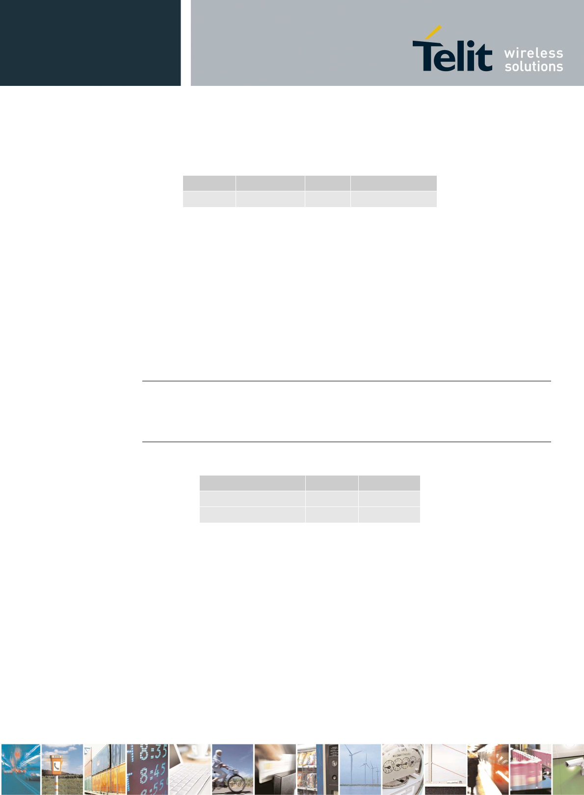
Note
NoteNote
Note:
::
:
If not used, almost all pins must be left disconnected. The only exceptions are the
following:
Pin
PinPin
Pin
Signal
SignalSignal
Signal
Function
FunctionFunction
Function
1
11
1
VBATT Main power supply
2
22
2
VBATT Main power supply
3
33
3
VBATT Main power supply
4
44
4
VBATT Main power supply
5
55
5
GND Ground
6
66
6
GND Ground
7
77
7
GND Ground
46
4646
46
GND Ground
25
2525
25
C103/TXD Serial data input (TXD) from DTE
26
2626
26
C104/RXD Serial data output to DTE
31
3131
31
C105/RTS Input for Request to send signal (RTS) from DTE
53
5353
53
ON/OFF Input command for switching power ON or OFF (toggle
command).
54
5454
54
RESET Reset input

UC864-E-AUTO / AWS-AUTO Hardware User Guide
1vv0300795 Rev.11 – 2010/11/18
Reproduction forbidden without Telit Communications S.p.A’s. written authorization - All Rights Reserved. Page 12 of 78
4. TEMPERATURE RANGE
TEMPERATURE RANGETEMPERATURE RANGE
TEMPERATURE RANGE
The UC864-E-AUTO / AWS-AUTO Temperature ranges are:
Reference Ambient Temperature
Reference Ambient TemperatureReference Ambient Temperature
Reference Ambient Temperature
Normal Operating -10°C to +55°C
Extended Operating -20°C to +70°C
Extreme Range -30°C to +85°C
Storage -40°C to +85°C
UC864-E-AUTO / AWS-AUTO Hardware User Guide
1vv0300795 Rev.11 – 2010/11/18
Reproduction forbidden without Telit Communications S.p.A’s. written authorization - All Rights Reserved. Page 13 of 78
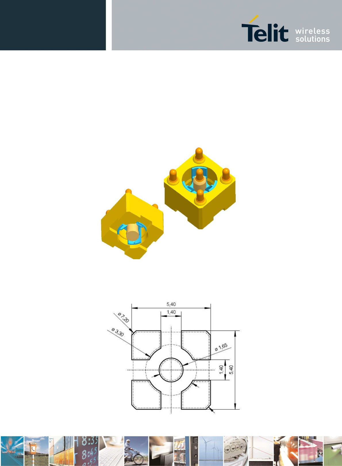
4.1. Antenna Connector(s)
The UC864-E-AUTO / AWS-AUTO module is designed with a 50 Ohm RF PAD that
permits to interface it with an application equipped by a Rosenberger coaxial Board
to board connector.
The counterpart suitable is a Rosenberger 99CI106-030L5.
Suggested footprint on the application side:

UC864-E-AUTO / AWS-AUTO Hardware User Guide
1vv0300795 Rev.11 – 2010/11/18
Reproduction forbidden without Telit Communications S.p.A’s. written authorization - All Rights Reserved. Page 14 of 78
5. Hardware Commands
Hardware CommandsHardware Commands
Hardware Commands
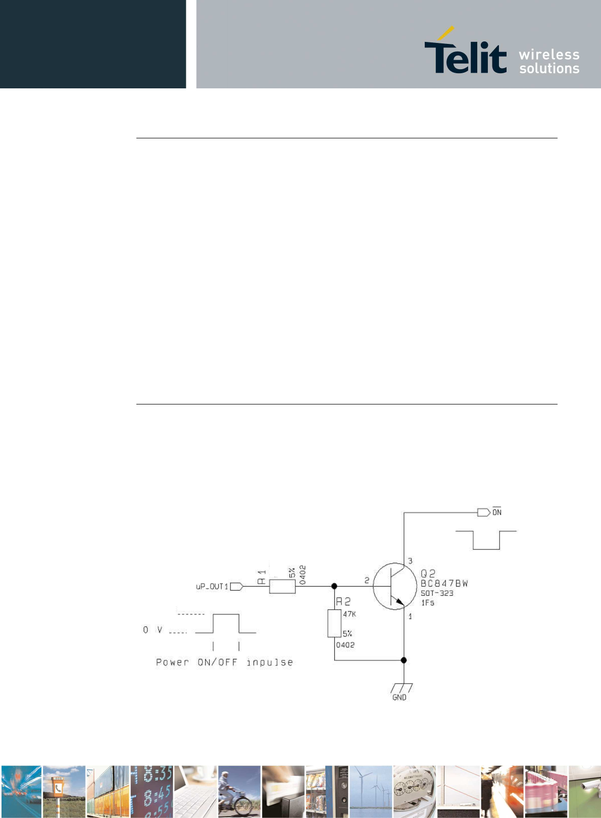
5.1. Turning ON the UC864-E-AUTO / AWS-AUTO
To turn on UC864-E-AUTO / AWS-AUTO, the pad ON# must be tied low for at least 1
second and then released.
The maximum current that can be drained from the ON# pad is 0,1 mA.
A simple
circuit
to do it is:
ON#
Power ON impulse
GND
R1
R2
Q1
UC864-E-AUTO / AWS-AUTO Hardware User Guide
1vv0300795 Rev.11 – 2010/11/18
Reproduction forbidden without Telit Communications S.p.A’s. written authorization - All Rights Reserved. Page 15 of 78
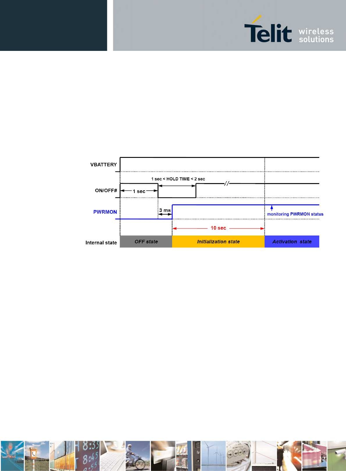
5.2. Initialization and Activation state
Upon turning on UC864-E-AUTO / AWS-AUTO, the module is not activated yet
because the boot sequence of UC864-E-AUTO / AWS-AUTO is still going on internally.
It takes about 10 seconds to complete the initializing the module internally.
For this reason, it would be useless to try to access UC864-E-AUTO/ AWS-AUTO
during a
Initialization state
as below. To get the desirable stability, UC864-E-AUTO /
AWS-AUTO needs at least 10 seconds after the PWRMON goes High.
During the
Initialization state
, any kind of AT-command is not available. DTE must be
waiting for the
Activation state
to communicate with UC864-E-AUTO / AWS-AUTO.
UC864-E-AUTO / AWS-AUTO Hardware User Guide
1vv0300795 Rev.11 – 2010/11/18
Reproduction forbidden without Telit Communications S.p.A’s. written authorization - All Rights Reserved. Page 16 of 78
For example:
1- Let us assume you need to drive the ON/OFF# pad with a totem pole output of a
+1.8/5 V microcontroller (uP_OUT1):
NOTE:
NOTE: NOTE:
NOTE:
To check if the UC864-E-AUTO / AWS-AUTO has powered on, the hardware line
PWRMON must be monitored. When PWRMON goes high, the module has powered
on.
NOTE:
NOTE: NOTE:
NOTE:
Do not use any pull up resistor on the ON/OFF# line, it is internally pulled up. Using
pull up resistor may bring to latch up problems on the UC864-E-AUTO / AWS-AUTO
power regulator and improper power on/off of the module. The line ON/OFF# must
be connected only in open collector configuration.
NOTE:
NOTE: NOTE:
NOTE:
In this document all the lines are inverted. Active low signals are labeled with a name
that ends with a "#" or with a bar over the name.
NOTE:
NOTE: NOTE:
NOTE:
UC864-E-AUTO / AWS-AUTO
turns fully on also by supplying power to the Charge pad
(provided there is a battery on the VBATT pads).
1s
10k
1.8 / 5V

UC864-E-AUTO / AWS-AUTO Hardware User Guide
1vv0300795 Rev.11 – 2010/11/18
Reproduction forbidden without Telit Communications S.p.A’s. written authorization - All Rights Reserved. Page 17 of 78
5.3. Turning OFF the UC864-E-AUTO / AWS-AUTO
Turning off the device can be done in three ways:
• by software command (see UC864-E-AUTO / AWS-AUTO Software User
Guide)
• by hardware shutdown
• by Hardware Unconditional Restart
When the device is shut down by software command or by hardware shutdown, it
issues to the network a detach request that informs the network that the device will
not be reachable any more.
UC864-E-AUTO / AWS-AUTO Hardware User Guide
1vv0300795 Rev.11 – 2010/11/18
Reproduction forbidden without Telit Communications S.p.A’s. written authorization - All Rights Reserved. Page 18 of 78
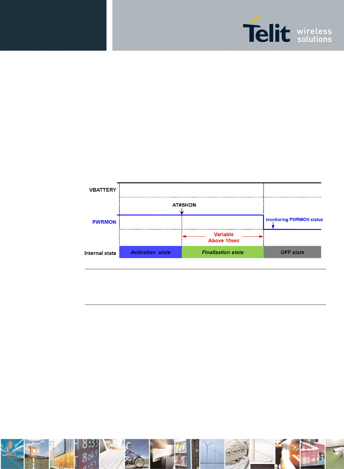
5.3.1. Shutdown by Software Command
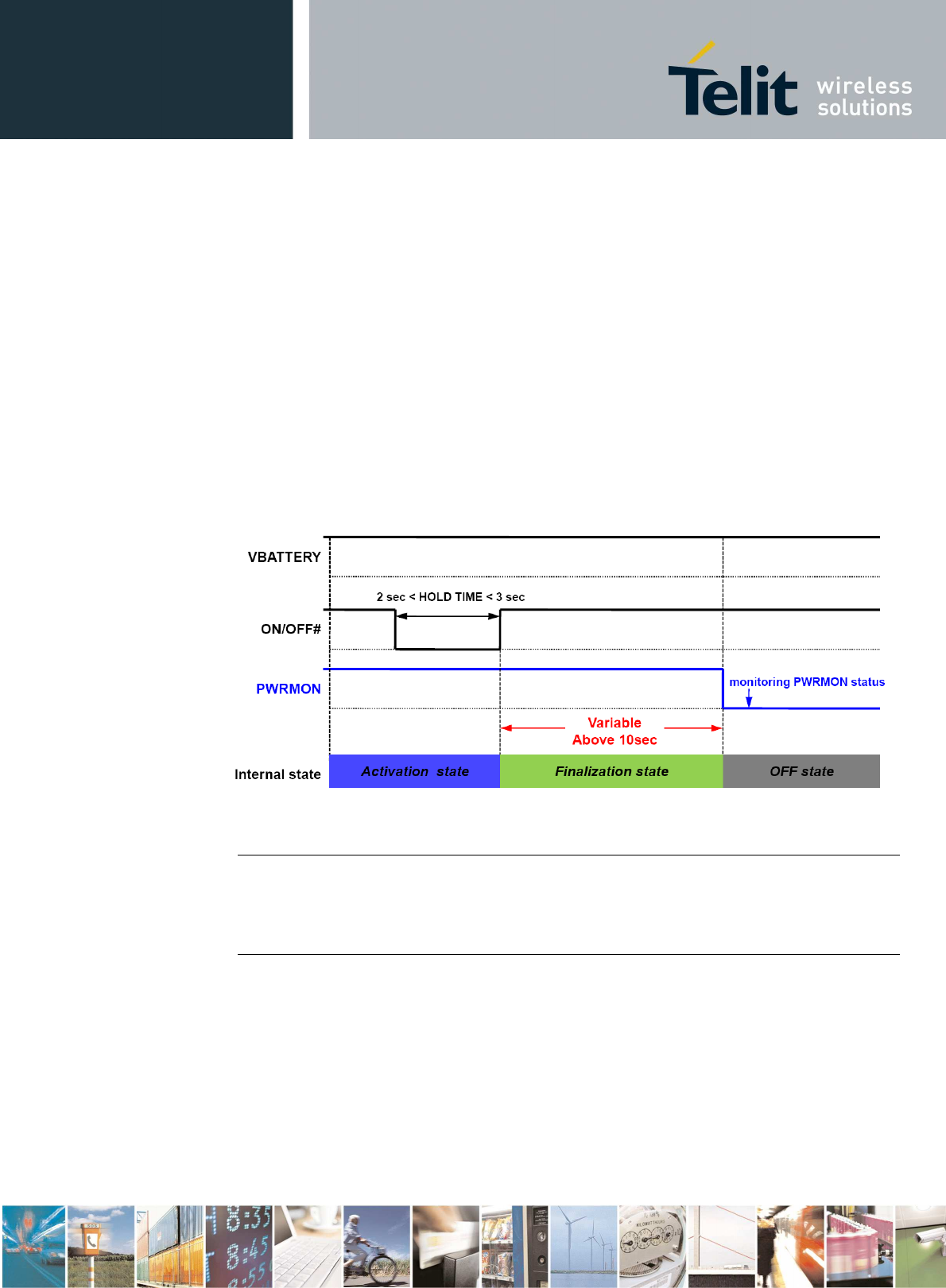
UC864-E-AUTO / AWS-AUTO can be shut down by a software command.
When a shut down command is sent, UC864-E-AUTO / AWS-AUTO goes into the
finalization state and finally will shut down PWRMON at the end of this state.
The period of the finalization state can differ according to the situation in which the
UC864-E-AUTO / AWS-AUTO is so it cannot be fixed definitely.
Normally it will be above 10 seconds later from sending a shut down command and
DTE should monitor the status of PWRMON to see the actual power off.
TIP:
TIP: TIP:
TIP:
To check if the device has powered off, hardware line PWRMON must be monitored.
When PWRMON goes low, the device has powered off.
UC864-E-AUTO / AWS-AUTO Hardware User Guide
1vv0300795 Rev.11 – 2010/11/18
Reproduction forbidden without Telit Communications S.p.A’s. written authorization - All Rights Reserved. Page 19 of 78
5.3.2. Hardware Shutdown
To turn OFF UC864-E-AUTO / AWS-AUTO the pad ON/OFF# must be tied low for at
least 2 seconds and then released. Same circuitry and timing for the power on must
be used.
When the hold time of ON/OFF# is above 2 seconds, UC864-E-AUTO / AWS-AUTO
goes into the finalization state and finally will shut down PWRMON at the end of this
state.
The period of the finalization state can differ according to the situation in which the
UC864-E-AUTO / AWS-AUTO is so it cannot be fixed definitely.
Normally it will be above 10 seconds later from releasing ON/OFF# and DTE should
monitor the status of PWRMON to see the actual power off.
TIP:
TIP: TIP:
TIP:
To check if the device has powered off, hardware line PWRMON must be monitored.
When PWRMON goes low, the device has powered off.

UC864-E-AUTO / AWS-AUTO Hardware User Guide
1vv0300795 Rev.11 – 2010/11/18
Reproduction forbidden without Telit Communications S.p.A’s. written authorization - All Rights Reserved. Page 20 of 78
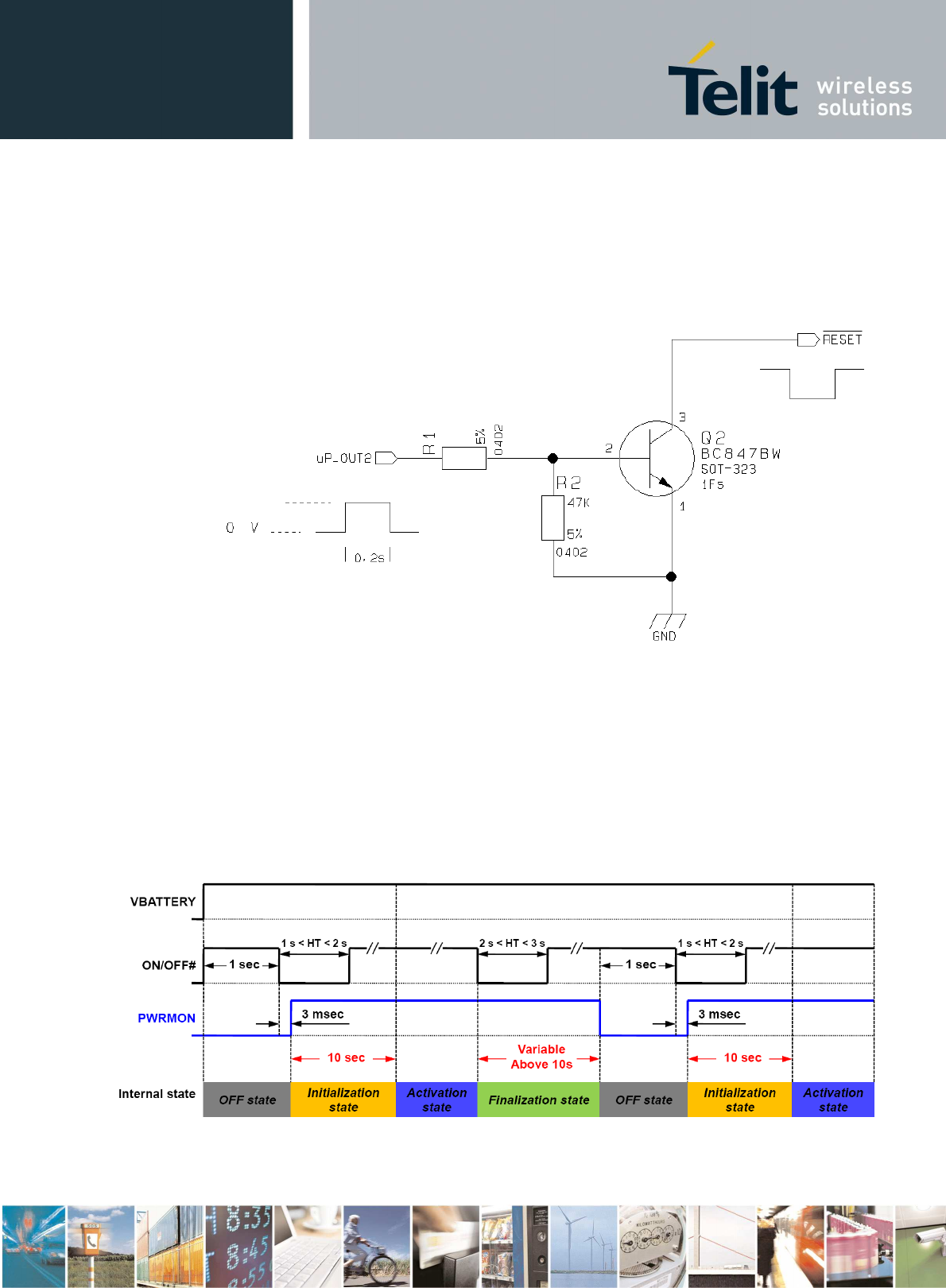
5.3.3. Hardware Unconditional Restart
To unconditionally restart UC864-E-AUTO / AWS-AUTO, the pad RESET# must be tied
low for at least 200 milliseconds and then released.
A simple circuit to do it is:
NOTE:
NOTE: NOTE:
NOTE:
Do not use any pull up resistor on the RESET# line or any totem pole digital output.
Using pull up resistor may bring to latch up problems on the UC864-E-AUTO / AWS-
AUTO power regulator and improper functioning of the module. The line RESET#
must be connected only in open collector configuration.
TIP:
TIP: TIP:
TIP:
The unconditional hardware Restart must always be implemented on the boards and
the software must use it as an emergency exit procedure.
RESET#
Unconditional Restart
impulse
GND
UC864-E-AUTO / AWS-AUTO Hardware User Guide
1vv0300795 Rev.11 – 2010/11/18
Reproduction forbidden without Telit Communications S.p.A’s. written authorization - All Rights Reserved. Page 21 of 78
For example:
1- Let us assume you need to drive the RESET# pad with a totem pole output of a
+1.8/5 V microcontroller (uP_OUT2):
5.4. Summary of Turning ON and OFF the module
Below chart describes the overall sequences for Turning ON and OFF.
10k
+1.8 / 5V
UC864-E-AUTO / AWS-AUTO Hardware User Guide
1vv0300795 Rev.11 – 2010/11/18
Reproduction forbidden without Telit Communications S.p.A’s. written authorization - All Rights Reserved. Page 22 of 78
6. Power Supply
Power SupplyPower Supply
Power Supply
The power supply circuitry and board layout are a very important part in the full
product design and they strongly reflect on the product overall performances. Read
carefully the requirements and the guidelines that will follow for a proper design.
6.1. Power Supply Requirements
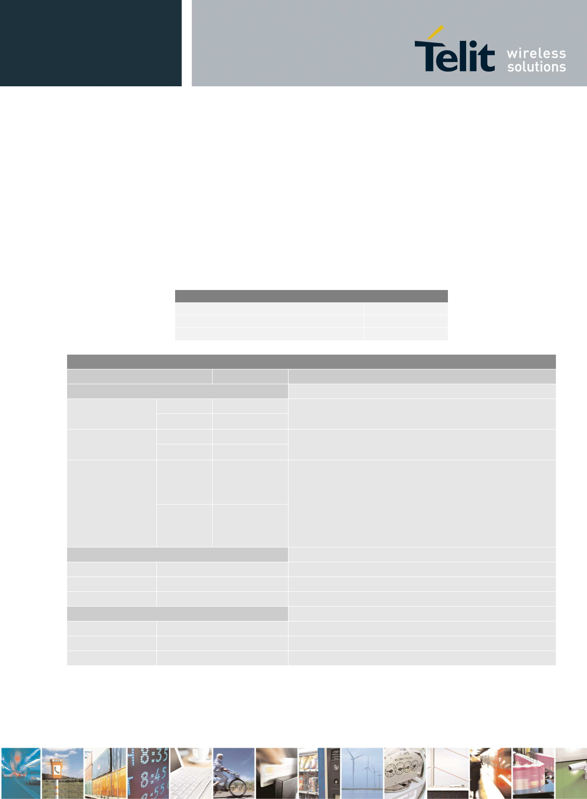
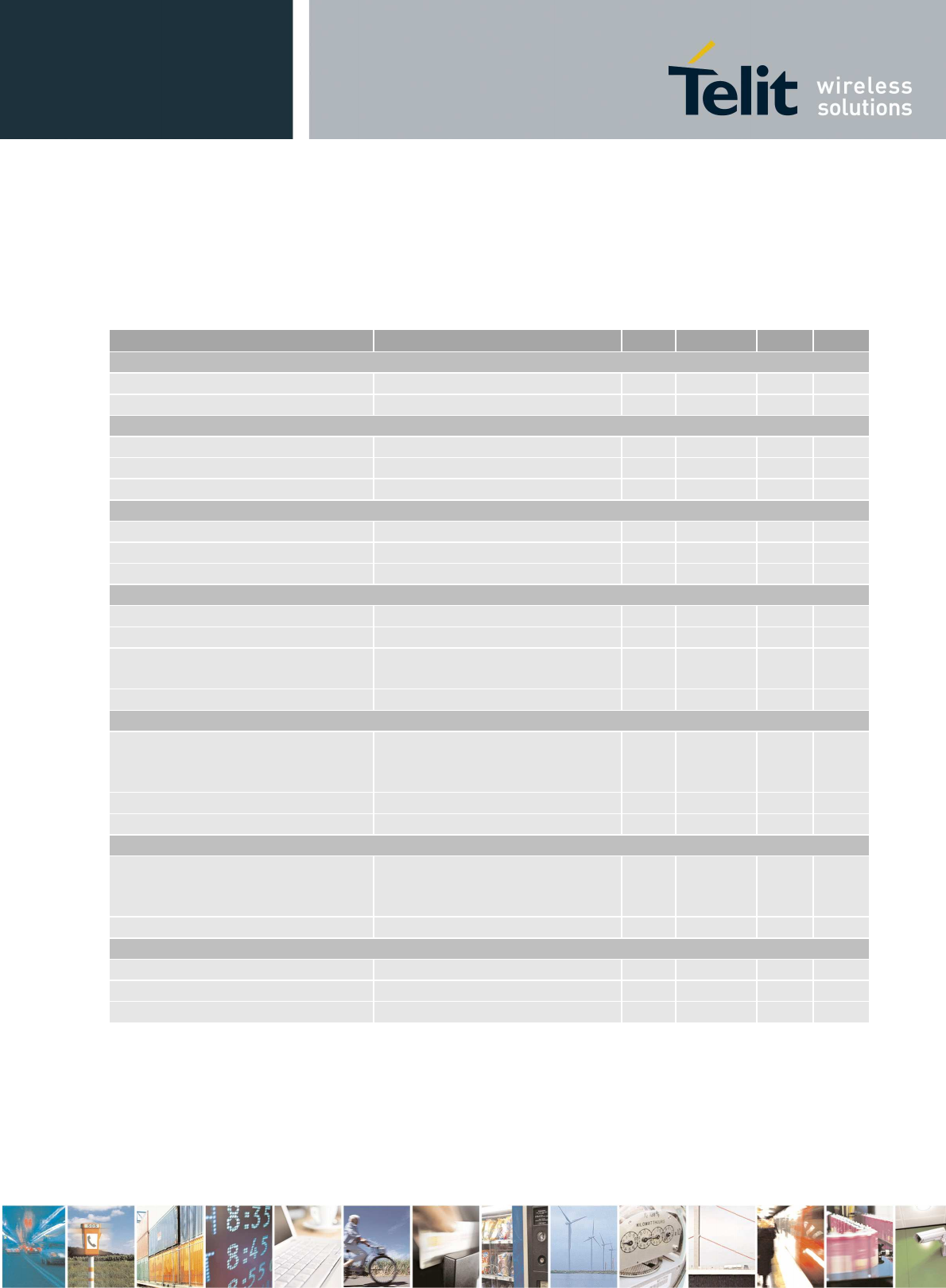
The UC864-E-AUTO / AWS-AUTO power requirements are:
Power Supply
Power SupplyPower Supply
Power Supply
Nominal Supply Voltage 3.8V
Max Supply Voltage 4.2V
Supply Voltage Range 3.4V – 4.2V
UC864
UC864UC864
UC864-
--
-E
EE
E-
--
-AUTO
AUTOAUTO
AUTO/ AWS
/ AWS/ AWS
/ AWS-
--
-AUTO
AUTOAUTO
AUTO
Mode
ModeMode
Mode
Average(mA)
Average(mA)Average(mA)
Average(mA)
Mode D
Mode DMode D
Mode Description
escriptionescription
escription
IDLE mode Stand by mode; no call in progress
AT+CFUN=1 WCDMA 22.0 Normal mode; full functionality of the module
GSM 15.0
AT+CFUN=4 WCDMA 17.8 Disabled TX and RX; modules is not registered on the
network
GSM 17.8
AT+CFUN=0 or
AT+CFUN=5
WCDMA 4.1 / 1.3*
Power saving; CFUN=0 module registered on the
network and can receive voice call or an SMS; but it is
not possible to send AT commands; module wakes up with
an unsolicited code (call or SMS) or rising RTS line.
CFN=5 full functionality with power saving;
Module registered on the network can receive
incoming call sand SMS
GSM 3.3 / 1.3*
WCDMA TX and RX mode
WCDMA Voice 690 WCDMA voice channel
WCDMA data 680 WCDMA data channel
HSDPA 730 HSDPA data channel
GSM TX and RX mode
GSM Voice 320 GSM voice channel
GPRS Class12 650 GPRS data channel
EDGE Class12 430 EDGE data channel
* Worst/best case depends on network configuration and is not under module control.

UC864-E-AUTO / AWS-AUTO Hardware User Guide
1vv0300795 Rev.11 – 2010/11/18
Reproduction forbidden without Telit Communications S.p.A’s. written authorization - All Rights Reserved. Page 23 of 78
In GSM/GPRS mode, RF transmission is not continuous and it is packed into bursts at
a base frequency of about 216 Hz, and the relative current peaks can be as high as
about 2A. Therefore the power supply has to be designed in order to withstand these
current peaks without big voltage drops; this means that both the electrical design
and the board layout must be designed for this current flow. If the layout of the PCB
is not well designed, a strong noise floor is generated on the ground; this will reflect
on all the audio paths producing an audible annoying noise at 216 Hz; if the voltage
drops during the peak, current absorption is too much. The device may even shut
down as a consequence of the supply voltage drop.
TIP:
TIP: TIP:
TIP:
The electrical design for the Power supply must be made ensuring that it will be
capable of a peak current output of at least 2A.

UC864-E-AUTO / AWS-AUTO Hardware User Guide
1vv0300795 Rev.11 – 2010/11/18
Reproduction forbidden without Telit Communications S.p.A’s. written authorization - All Rights Reserved. Page 24 of 78
6.2. General Design Rules
The principal guidelines for the Power Supply Design embrace three different design
steps:
• the electrical design
• the thermal design
• the PCB layout
6.2.1. Electrical Design Guidelines
The electrical design of the power supply depends strongly on the power source
where this power is drained. We will distinguish them into three categories:
• +5V input (typically PC internal regulator output)
• +12V input (typically automotive)
• battery
6.2.1.1. + 5V Input Source Power Supply Design Guidelines
• The desired output for the power supply is 3.8V, hence there is not a big
difference between the input source and the desired output and a linear
regulator can be used. A switching power supply will not be suited
because of the low drop-out requirements.
• When using a linear regulator, a proper heat sink must be provided in
order to dissipate the power generated.
• A Bypass low ESR capacitor of adequate capacity must be provided in
order to cut the current absorption peaks close to UC864-E-AUTO / AWS-
AUTO, a 100µF tantalum capacitor is usually suited.
• Make sure the low ESR capacitor on the power supply output (usually a
tantalum one) is rated at least 10V.
• A protection diode must be inserted close to the power input, in order to
save UC864-E-AUTO / AWS-AUTO from power polarity inversion.

UC864-E-AUTO / AWS-AUTO Hardware User Guide
1vv0300795 Rev.11 – 2010/11/18
Reproduction forbidden without Telit Communications S.p.A’s. written authorization - All Rights Reserved. Page 25 of 78
An example of linear regulator with 5V input is:
6.2.1.2. + 12V Input Source Power Supply Design Guidelines
• The desired output for the power supply is 3.8V, hence due to the big
difference between the input source and the desired output, a linear
regulator is not suited and must not be used. A switching power supply
will be preferable because of its better efficiency especially with the 2A
peak current load represented by UC864-E-AUTO / AWS-AUTO.
• When using a switching regulator, a 500kHz or more switching frequency
regulator is preferable because of its smaller inductor size and its faster
transient response. This allows the regulator to respond quickly to the
current peaks absorption.
• In any case, the frequency and Switching design selection is related to the
application to be developed due to the fact the switching frequency could
also generate EMC interferences.
• For car PB battery the input voltage can rise up to 15.8V and this must be
kept in mind when choosing components: all components in the power
supply must withstand this voltage.
• A Bypass low ESR capacitor of adequate capacity must be provided in
order to cut the current absorption peaks. A 100µF tantalum capacitor is
usually suited for this.

UC864-E-AUTO / AWS-AUTO Hardware User Guide
1vv0300795 Rev.11 – 2010/11/18
Reproduction forbidden without Telit Communications S.p.A’s. written authorization - All Rights Reserved. Page 26 of 78
• Make sure the low ESR capacitor on the power supply output (usually a
tantalum one) is rated at least 10V.
• For Car applications a spike protection diode must be inserted close to
the power input, in order to clean the supply from spikes.
• A protection diode must be inserted close to the power input, in order to
save UC864-E-AUTO / AWS-AUTO from power polarity inversion. This can
be the same diode as for spike protection.
An example of switching regulator with 12V input is in the below schematic (it is split
in 2 parts):

UC864-E-AUTO / AWS-AUTO Hardware User Guide
1vv0300795 Rev.11 – 2010/11/18
Reproduction forbidden without Telit Communications S.p.A’s. written authorization - All Rights Reserved. Page 27 of 78
6.2.1.3. Battery Source Power Supply Design Guidelines
• The desired nominal output for the power supply is 3.8V and the
maximum allowed voltage is 4.2V, hence a single 3.7V Li-Ion cell battery
type is suited for supplying the power to the Telit UC864-E-AUTO / AWS-
AUTO module. The three cells Ni/Cd or Ni/MH 3.6 V Nom. battery types or
4V PB types must not be used directly since their maximum voltage can
rise over the absolute maximum voltage for UC864-E-AUTO / AWS-AUTO
and damage it.
• A Bypass low ESR capacitor of adequate capacity must be provided in
order to cut the current absorption peaks, a 100µF tantalum capacitor is
usually suited.
• Make sure the low ESR capacitor (usually a tantalum one) is rated at least
10V.
• A protection diode must be inserted close to the power input, in order to
save UC864-E-AUTO / AWS-AUTO from power polarity inversion.
Otherwise the battery connector must be done in a way to avoid polarity
inversions when connecting the battery.
• The battery capacity must be at least 500mAh in order to withstand the
current peaks of 2A; the suggested capacity is from 500mAh to 1000mAh.
NOTE:
NOTE: NOTE:
NOTE:
Do not use any Ni-Cd, Ni-MH, and Pb battery types directly connected with UC864-E-
AUTO / AWS-AUTO. Their use can lead to overvoltage on UC864-E-AUTO / AWS-AUTO
and damage it. Use only Li-Ion battery types.

UC864-E-AUTO / AWS-AUTO Hardware User Guide
1vv0300795 Rev.11 – 2010/11/18
Reproduction forbidden without Telit Communications S.p.A’s. written authorization - All Rights Reserved. Page 28 of 78
6.2.1.4. Battery Charge Control Circuitry Design Guidelines
The charging process for Li-Ion Batteries can be divided into 4 phases:
• qualification and trickle charging
• fast charge 1 - constant current
• final charge - constant voltage or pulsed charging
• maintenance charge
The qualification process consists of a battery voltage measure, indicating roughly its
charge status. If the battery is deeply discharged, meaning its voltage is lower than
the trickle charging threshold, then charging must start slowly, possibly with a
current limited to the pre-charging process. The current must be kept very low with
respect to the fast charge value.
During trickle charging the voltage across the battery terminals rises; when it
reaches the fast charge threshold level the charging process goes into a fast charge
phase.
During the fast charge phase the process proceeds with a current limited for
charging; this current limit depends on the required time for completing the charge
and on battery pack capacity. During this phase the voltage across the battery
terminals still raises but at a lower rate. Once the battery voltage reaches its
maximum voltage the process goes into its third state: Final charging. The voltage
measure to change the process status into final charge is very important. It must be
ensured that the maximum battery voltage is never exceeded, otherwise the battery
may be damaged and even explode.
Moreover, for constant final chargers, the voltage phase (final charge) must not start
before the battery voltage has reached its maximum value, otherwise the battery
capacity will be slightly reduced. The final charge can be of two different types:
constant voltage or pulsed. UC864-E-AUTO / AWS-AUTO uses constant voltage.
The constant voltage charge proceeds with a fixed voltage regulator (very accurately
set to the maximum battery voltage) and the current will decrease while the battery
is becoming charged. When the charging current falls below a certain fraction of the
fast charge current value, the battery is considered fully charged, the final charge
stops and eventually starts the maintenance.
The pulsed charge process has no voltage regulation, instead charge continues with
pulses. Usually the pulse charge works in the following manner: the charge is
stopped for some time, let us say few hundreds of ms, then the battery voltage will
be measured and when it drops below its maximum value, a fixed time length
charging pulse is issued. As the battery approaches its full charge, the off time will
become longer and the duty-cycle of the pulses will decrease. The battery is
considered fully charged when the pulse duty-cycle is less than a threshold value,

UC864-E-AUTO / AWS-AUTO Hardware User Guide
1vv0300795 Rev.11 – 2010/11/18
Reproduction forbidden without Telit Communications S.p.A’s. written authorization - All Rights Reserved. Page 29 of 78
typically 10%. When this happens, the pulse charge stops and eventually the
maintenance starts.
The last phase is not properly a charging phase, since the battery at this point is fully
charged and the process may stop after the final charge. The maintenance charge
provides an additional charging process to compensate the charge leak typical of a
Li-Ion battery. It is done by issuing pulses with a fixed time length, again few
hundreds of ms, and a duty-cycle around 5% or less.
This last phase is not implemented in the UC864-E-AUTO / AWS-AUTO internal
charging algorithm so once-charged battery is left discharging down to a certain
threshold. It is cycled from full charge to slight discharge even if the battery charger
is inserted. This guarantees that the remaining charge in the battery is a good
percentage and that the battery is not damaged by keeping it always fully charged
(Li-Ion rechargeable batteries usually deteriorate when kept fully charged).
Last but not least, in some applications, it is highly desired that the charging process
restarts when the battery is discharged and its voltage drops below a certain
threshold. This is typical for the UC864-E-AUTO / AWS-AUTO internal charger.
As you can see, the charging process is not a trivial task to do; moreover all these
operations must start only if battery temperature is inside charging range, usually
5°C - 45°C.
The UC864-E-AUTO / AWS-AUTO measures the temperature of its internal
component in order to satisfy this last requirement. This not exactly the same as the
battery temperature but in common use, the two temperatures must not differ too
much and the charging temperature range must be guaranteed.

UC864-E-AUTO / AWS-AUTO Hardware User Guide
1vv0300795 Rev.11 – 2010/11/18
Reproduction forbidden without Telit Communications S.p.A’s. written authorization - All Rights Reserved. Page 30 of 78
6.2.2. Thermal Design Guidelines
The thermal design for the power supply heat sink must be done with the following
specifications:
• Average current consumption during HSDPA transmission @PWR level
max in UC864-E-AUTO / AWS-AUTO : 730mA
• Average current consumption during class12 GPRS transmission @PWR
level max: 650mA
NOTE:
NOTE: NOTE:
NOTE:
For all the threshold voltages, inside UC864-E-AUTO / AWS-AUTO, all thresholds are
fixed in order to maximize Li-Ion battery performances and do not need to be
changed.
NOTE:
NOTE: NOTE:
NOTE:
In this application the battery charger input current must be limited to less than
400mA. This can be done by using a current limited wall adapter as the power
source.
NOTE:
NOTE: NOTE:
NOTE:
When starting the charger from Module powered off, the startup will be in CFUN4; to
activate the normal mode a command AT+CFUN=1 has to be provided.
There is also the possibility to activate the normal mode using the ON_OFF* signal.
In this case, when HW powering off the module with the same line (ON_OFF*) and
having the charger still connected, the module will go back to CFUN4.
NOTE:
NOTE:NOTE:
NOTE:
It is important to have a 100ųF Capacitor to VBAT in order to avoid instability of the
charger circuit if the battery is accidentally disconnected during the charging activity.

UC864-E-AUTO / AWS-AUTO Hardware User Guide
1vv0300795 Rev.11 – 2010/11/18
Reproduction forbidden without Telit Communications S.p.A’s. written authorization - All Rights Reserved. Page 31 of 78
Considering the very low current during idle, especially if Power Saving function is
enabled, it is possible to consider from the thermal point of view that the device
absorbs current significantly only during calls.
If we assume that the device stays in transmission for short periods of time (let us
say few minutes) and then remains for quite a long time in idle (let us say one hour),
then the power supply has always the time to cool down between the calls and the
heat sink could be smaller than the calculated for 730mA maximum RMS current.
There could even be a simple chip package (no heat sink).
Moreover in average network conditions the device is requested to transmit at a
lower power level than the maximum and hence the current consumption will be less
than 730mA (being usually around 250mA).
For these reasons the thermal design is rarely a concern and the simple ground
plane where the power supply chip is placed can be enough to ensure a good thermal
condition and avoid overheating.
For the heat generated by the UC864-E-AUTO / AWS-AUTO, you can consider it to be
during transmission 2W max. This generated heat will be mostly conducted to the
ground plane under the UC864-E-AUTO / AWS-AUTO; you must ensure that your
application can dissipate heat
In the WCDMA/HSDPA mode, since UC864-E-AUTO / AWS-AUTO emits RF signals
continuously during transmission, you must pay special attention how to dissipate
the heat generated.
The current consumption will be up to about 730mA in HSDPA (680mA in WCDMA)
continuously at the maximum TX output power (24dBm). Thus, you must arrange the
PCB area as large as possible under UC864-E-AUTO / AWS-AUTO which you will
mount. You must mount UC864-E-AUTO / AWS-AUTO on the large ground area of
your application board and make many ground vias to dissipate the heat.
The peak current consumption in the GSM mode is higher than that in WCDMA.
However, considering the heat sink is more important in case of WCDMA.
NOTE:
NOTE: NOTE:
NOTE:
The average consumption during transmissions depends on the power level at which
the device is requested to transmit via the network. The average current
consumption hence varies significantly.
NOTE:
NOTE: NOTE:
NOTE:
The thermal design for the Power supply must be made keeping an average
consumption at the max transmitting level during calls of 730mA rms.

UC864-E-AUTO / AWS-AUTO Hardware User Guide
1vv0300795 Rev.11 – 2010/11/18
Reproduction forbidden without Telit Communications S.p.A’s. written authorization - All Rights Reserved. Page 32 of 78
As mentioned before, a GSM signal is bursty, thus, the temperature drift is more
insensible than WCDMA. Consequently, if you prescribe the heat dissipation in the
WCDMA mode, you don’t need to think more about the GSM mode.
6.2.3. Power Supply PCB Layout Guidelines
As seen in the electrical design guidelines, the power supply must have a low ESR
capacitor on the output to cut the current peaks and a protection diode on the input
to protect the supply from spikes and polarity inversion. The placement of these
components is crucial for the correct working of the circuitry. A misplaced
component can be useless or can even decrease the power supply performances.
• The Bypass low ESR capacitor must be placed close to the Telit UC864-E-
AUTO / AWS-AUTO power input pads, or in the case the power supply is a
switching type, it can be placed close to the inductor to cut the ripple if the
PCB trace from the capacitor to UC864-E-AUTO / AWS-AUTO is wide
enough to ensure a drop-less connection even during the 2A current
peaks.
• The protection diode must be placed close to the input connector where
the power source is drained.
• The PCB traces from the input connector to the power regulator. IC must
be wide enough to ensure no voltage drops to occur when the 2A current
peaks are absorbed. Note that this is not made in order to save power
loss but especially to avoid the voltage drops on the power line at the
current peaks frequency of 216 Hz that will reflect on all the components
connected to that supply (also introducing the noise floor at the burst
base frequency.) For this reason while a voltage drop of 300-400 mV may
be acceptable from the power loss point of view, the same voltage drop
may not be acceptable from the noise point of view. If your application
does not have audio interface but only uses the data feature of the Telit
UC864-E-AUTO, then this noise is not so disturbing and power supply
layout design can be more forgiving.
• The PCB traces to UC864-E-AUTO / AWS-AUTO and the Bypass capacitor
must be wide enough to ensure no significant voltage drops to occur when
the 2A current peaks are absorbed. This is a must for the same above-
mentioned reasons. Try to keep this trace as short as possible.
• The PCB traces connecting the Switching output to the inductor and the
switching diode must be kept as short as possible by placing the inductor
and the diode very close to the power switching IC (only for switching
power supply). This is done in order to reduce the radiated field (noise) at
the switching frequency (usually 100-500 kHz).
• The use of a good common ground plane is suggested.

UC864-E-AUTO / AWS-AUTO Hardware User Guide
1vv0300795 Rev.11 – 2010/11/18
Reproduction forbidden without Telit Communications S.p.A’s. written authorization - All Rights Reserved. Page 33 of 78
• The placement of the power supply on the board must be done in a way to
guarantee that the high current return paths in the ground plane are not
overlapped to any noise sensitive circuitry as the microphone
amplifier/buffer or earphone amplifier.
• The power supply input cables must be kept separately from noise
sensitive lines such as microphone/earphone cables.
UC864-E-AUTO / AWS-AUTO Hardware User Guide
1vv0300795 Rev.11 – 2010/11/18
Reproduction forbidden without Telit Communications S.p.A’s. written authorization - All Rights Reserved. Page 34 of 78
7. Antenna
AntennaAntenna
Antenna(s)
(s)(s)
(s)
The antenna connection and board layout design are the most important parts in the
full product design and they strongly reflect on the product’s overall performances.
Read carefully and follow the requirements and the guidelines for a proper design.
7.1. GSM/WCDMA Antenna Requirements
As suggested on the Product Description, the antenna for a Telit UC864-E-AUTO /
AWS-AUTO device must fulfill the following requirements:
Furthermore if the device is developed for the US market, it must comply to the FCC
approval requirements:
This device is to be used only for mobile and fixed application. The antenna(s) used
for this transmitter must be installed to provide a separation distance of at least 20
cm from all persons and must not be co-located or operating in conjunction with any
other antenna or transmitter. End-Users must be provided with transmitter
operation conditions for satisfying RF exposure compliance. OEM integrators must
ensure that the end user has no manual instructions to remove or install the UC864-
AWS-AUTO module
.
Antennas used for this OEM module must not exceed
7
.18 dBi
(GSM 850), 2.78 dBi (PCS 1900) and 1.43 dBi (FDD IV)
gain for mobile and fixed
operating configurations.
GSM /WCDMA ANTENNA REQUIREMENTS
GSM /WCDMA ANTENNA REQUIREMENTSGSM /WCDMA ANTENNA REQUIREMENTS
GSM /WCDMA ANTENNA REQUIREMENTS
Frequency range
Frequency rangeFrequency range
Frequency range
Depending by frequency band(s) provided by the network
operator, the customer shall use the most suitable antenna for
that/those band(s)
Bandwidth
BandwidthBandwidth
Bandwidth
UC864
UC864UC864
UC864-
--
-E
EE
E-
--
-AUTO
AUTOAUTO
AUTO
80 MHz in GSM900, 170 MHz in DCS
250 MHz in WCDMA2100 band
UC864
UC864UC864
UC864-
--
-AWS
AWSAWS
AWS-
--
-AUTO
AUTOAUTO
AUTO
70 MHz in GSM850, 140 MHz in PCS
455 MHz in WCDMA1700(AWS) band
WCDMA AWS band : TX = 45MHz, RX = 45MHz
TX-RX freq. separation = 400MHz
Gain
GainGain
Gain
Gain <
7.18 dBi (GSM 850), 2.78 dBi (PCS 1900) and 1.43 dBi (FDD
IV)
Impedance
ImpedanceImpedance
Impedance
50 Ohm
Input power
Input powerInput power
Input power
> 33dBm(2 W) peak power in GSM
> 24dBm Average power in WCDMA
VSWR absolute max
VSWR absolute maxVSWR absolute max
VSWR absolute max
<= 10:1
VSWR recommended
VSWR recommendedVSWR recommended
VSWR recommended
<= 2:1

UC864-E-AUTO / AWS-AUTO Hardware User Guide
1vv0300795 Rev.11 – 2010/11/18
Reproduction forbidden without Telit Communications S.p.A’s. written authorization - All Rights Reserved. Page 35 of 78
7.2. GSM/WCDMA Antenna - Installation Guidelines
• Install the antenna in a place covered by the GSM/WCDMA signal.
• The Antenna must be installed to provide a separation distance of at least
20 cm from all persons and must not be co-located or operating in
conjunction with any other antenna or transmitter;
• Antenna must not be installed inside metal cases;
• Antenna must be installed also according Antenna manufacturer
instructions.
UC864-E-AUTO / AWS-AUTO Hardware User Guide
1vv0300795 Rev.11 – 2010/11/18
Reproduction forbidden without Telit Communications S.p.A’s. written authorization - All Rights Reserved. Page 36 of 78
8. Logic L
Logic LLogic L
Logic Level
evel evel
evel S
SS
Specifications
pecificationspecifications
pecifications
Where not specifically stated, all the interface circuits work at 2.6V CMOS logic
levels. The following table shows the logic level specifications used in the Telit
UC864-E-AUTO / AWS-AUTO interface circuits:
For 2.6V CMOS signals:
Absolute Maximum Ratings
Absolute Maximum Ratings Absolute Maximum Ratings
Absolute Maximum Ratings -
--
-Not Functional
Not FunctionalNot Functional
Not Functional
Parameter
ParameterParameter
Parameter
UC864
UC864UC864
UC864-
--
-E
EE
E-
--
-AUTO
AUTOAUTO
AUTO
/ AWS
/ AWS/ AWS
/ AWS-
--
-AUTO
AUTOAUTO
AUTO
Min
MinMin
Min
Max
MaxMax
Max
Input level on any
digital pin when on -0.3V +3.0V
Input voltage on
analog pins when on
-0.3V +3.0 V
Ope
OpeOpe
Operating Range
rating Range rating Range
rating Range -
--
-
Interface levels
Interface levelsInterface levels
Interface levels
Level
LevelLevel
Level
UC864
UC864UC864
UC864-
--
-E
EE
E-
--
-AUTO
AUTOAUTO
AUTO
/ AWS
/ AWS/ AWS
/ AWS-
--
-AUTO
AUTOAUTO
AUTO
Min
MinMin
Min
Max
MaxMax
Max
Input high level 2.0V 2.9 V
Input low level -0.3V 0.6V
Output high level 2.15V 2.6V
Output low level 0V 0.45V
For 1,8V signals:
Operating Range
Operating Range Operating Range
Operating Range -
--
-
Interface levels (1.8V CMOS)
Interface levels (1.8V CMOS)Interface levels (1.8V CMOS)
Interface levels (1.8V CMOS)
Lev
LevLev
Level
elel
el
UC864
UC864UC864
UC864-
--
-E
EE
E-
--
-AUTO
AUTOAUTO
AUTO
/ AWS
/ AWS/ AWS
/ AWS-
--
-AUTO
AUTOAUTO
AUTO
Min
MinMin
Min
Max
MaxMax
Max
Input high level 1.5V 2.1V
Input low level -0.3V 0.5V
Output high level 1.35V 1.8V
Output low level 0V 0.45V
NOTE:
NOTE: NOTE:
NOTE:
Do not connect UC864-E-AUTO / AWS-AUTO’s digital logic signal directly to OEM’s
digital logic signal of with level higher than 3.0V.
UC864-E-AUTO / AWS-AUTO Hardware User Guide
1vv0300795 Rev.11 – 2010/11/18
Reproduction forbidden without Telit Communications S.p.A’s. written authorization - All Rights Reserved. Page 37 of 78
8.1. Reset Signal
Signal
SignalSignal
Signal
Function
FunctionFunction
Function
I/O
I/OI/O
I/O
PIN Number
PIN NumberPIN Number
PIN Number
RESET Phone reset
I 54
RESET is used to reset the UC864-E-AUTO / AWS-AUTO module. Whenever this
signal is pulled low, UC864-E-AUTO / AWS-AUTO is reset. When the device is reset it
stops all operations. After the release of the reset UC864-E-AUTO / AWS-AUTO is
unconditionally shut down, without doing any detach operations from the network
where it is registered. This behavior is not a proper shutdown because the device is
requested to issue a detach request on turn off. For this reason, the Reset signal
must not be used for normally shutting down the device, but only as an emergency
exit in the rare case the device remains stuck waiting for some network response.
The RESET is internally controlled on start-up to achieve always a proper power-on
reset sequence. There is no need to control this pin on start-up. It may only be used
to reset a device already on, that is, not responding to any command.
Reset Signal Operating levels:
Signal
SignalSignal
Signal
Min
MinMin
Min
Max
MaxMax
Max
RESET Input high 2.0V* 2.6V
RESET Input low 0V 0.2V
* This signal is internally pulled up so the pin can be left floating if not used.
If unused, this signal may be left unconnected. If used, it must always be connected
with an open collector transistor to permit the internal circuitry the power on reset
and under voltage lockout functions.
NOTE:
NOTE: NOTE:
NOTE:
Do not use this signal to power off UC864-E-AUTO / AWS-AUTO. Use the ON/OFF
signal to perform this function or the AT#SHDN command.

UC864-E-AUTO / AWS-AUTO Hardware User Guide
1vv0300795 Rev.11 – 2010/11/18
Reproduction forbidden without Telit Communications S.p.A’s. written authorization - All Rights Reserved. Page 38 of 78
9. USB Port
USB PortUSB Port
USB Port
UC864-E-AUTO / AWS-AUTO includes an integrated universal serial bus (USB)
transceiver, compatible with USB 2.0 specifications and supporting the USB Full-
Speed (12 Mb/s) mode. In HSDPA (High Speed downlink Packet Access) mode, the
downlink data speed rates up to 7.2Mbps. Hence OEMs need to interface UC864-E-
AUTO / AWS-AUTO to applications in full-speed (12Mbits/s) mode.
This is the main communication port suggested for the OEM application.
Signal
SignalSignal
Signal
UC864
UC864UC864
UC864-
--
-E
EE
E-
--
-AUTO
AUTOAUTO
AUTO
/ AWS
/ AWS/ AWS
/ AWS-
--
-AUTO
AUTOAUTO
AUTO
Pad No.
Pad No.Pad No.
Pad No.
Usage
UsageUsage
Usage
USB_VBUS 48
Power supply for the internal USB transceiver. This pin is configured
as an analog input or an analog output depending upon the type of
peripheral device connected.
USB_D- 80 Minus (-) line of the differential, bi-directional USB signal to/from the
peripheral device
USB D+ 79 Plus (+) line of the differential, bi-directional USB signal to/from the
peripheral device
USB_ID
(for future use) 35
Analog input used to sense whether a peripheral device is
connected and if connected, to determine the peripheral type, host or
slave
NOTE:
NOTE:NOTE:
NOTE:
UC864-E-AUTO / AWS-AUTO
does NOT support host device operation at the moment,
that is, it works as a slave device. Consequently USB_ID must be opened (not
connected).
UC864-E-AUTO / AWS-AUTO Hardware User Guide
1vv0300795 Rev.11 – 2010/11/18
Reproduction forbidden without Telit Communications S.p.A’s. written authorization - All Rights Reserved. Page 39 of 78
9.1. USB transceiver specifications
This is the on-chip USB transceiver specifications
Parameter
ParameterParameter
Parameter
Comments
CommentsComments
Comments
Min
MinMin
Min
Typ
TypTyp
Typ
Max
MaxMax
Max
Unit
UnitUnit
Unit
USB_VBUS
USB_VBUSUSB_VBUS
USB_VBUS
:
::
:
Supply Voltage 4.5 5.0 5.25 V
Supply Current 25 mA
Input Lev
Input LevInput Lev
Input Levels for Low
els for Lowels for Low
els for Low-
--
-/full
/full/full
/full-
--
-speed :
speed :speed :
speed :
Receiver Threshold (single-end) 0.8 2.0 V
Differential Input Sensitivity |D+ - D-|, V
IN
= 0.8V to 2.5V 0.2 V
Differential Common-mode Range Includes V
DI
0.8 2.5 V
Output Levels for Low
Output Levels for LowOutput Levels for Low
Output Levels for Low-
--
-/full
/full/full
/full-
--
-speed :
speed :speed :
speed :
Low R
L
= 1.5 kΩ to 3.6 V 0.3 V
High R
L
= 15 kΩ to GND 2.8 3.6 V
Output Signal Crossover Voltage 1.3 2.0 V
Terminations :
Terminations :Terminations :
Terminations :
Internal pull-up resistor V
TRM
to D+, V
TRM
to D- 1.425
1.5 1.575
kΩ
Internal pull-down resistor D+ to GND, D- to GND 14.3 15 24.8 kΩ
High-Z state output impedance 0 V < V
D
< 3.6V; measured at D+
and D- pins to GND 300 kΩ
Termination Voltage An internal supply voltage, V
TRM
3.0 3.3 3.6 V
Driver
Driver Driver
Driver c
cc
characteristics
haracteristics haracteristics
haracteristics –
––
–
F
FF
Full speed
ull speedull speed
ull speed
Transition time :
Rise time
Fall time
C
L
= 50 to 125 pF
C
L
= 50 to 125 pF
4
4
20
20
ns
ns
Rise/fall time matching 90 111 %
Series output resistance D+, D- 28 33 44 Ω
Driver characteristics
Driver characteristics Driver characteristics
Driver characteristics –
––
–
L
LL
Low speed
ow speedow speed
ow speed
Transition time :
Rise time
Fall time
C
L
= 50 to 600 pF
C
L
= 50 to 600 pF
75
75
300
300
ns
ns
Rise/fall time matching 80 125 %
USB_ID (for future use only)
USB_ID (for future use only)USB_ID (for future use only)
USB_ID (for future use only)
ID pin pull-up resistance 108 140 182 kΩ
A device detection threshold t
delay
< 1 us, V
hys
= 50mV
0.15*V
TRM
V
B device detection threshold t
delay
< 1 us, V
hys
= 50mV
0.8*V
TRM
V

UC864-E-AUTO / AWS-AUTO Hardware User Guide
1vv0300795 Rev.11 – 2010/11/18
Reproduction forbidden without Telit Communications S.p.A’s. written authorization - All Rights Reserved. Page 40 of 78
10. Serial Ports
Serial PortsSerial Ports
Serial Ports
The serial port on the Telit UC864-E-AUTO / AWS-AUTO is another possible interface
between the module and OEM hardware.
2 serial ports are available on the module:
• MODEM SERIAL PORT;
• MODEM SERIAL PORT 2 (DEBUG).
10.1. Modem Serial Port
Several configurations can be designed for the serial port on the OEM hardware. The
most common are:
• RS232 PC com port;
• microcontroller UART @ 2.6V – 2.9V (Universal Asynchronous Receive
Transmit) ;
• microcontroller UART @ 5V or other voltages different from 2.6V .
Depending on the type of serial port on the OEM hardware, a level translator circuit
may be needed to make the system work. The only configuration that does not need a
level translation is the 2.6V UART.
The serial port on UC864-E-AUTO / AWS-AUTO is a +2.6V UART with all the 7 RS232
signals. It differs from the PC-RS232 in signal polarity (RS232 is reversed) and levels.
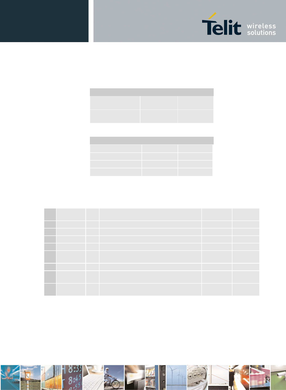
UC864-E-AUTO / AWS-AUTO Hardware User Guide
1vv0300795 Rev.11 – 2010/11/18
Reproduction forbidden without Telit Communications S.p.A’s. written authorization - All Rights Reserved. Page 41 of 78
The levels for UC864-E-AUTO / AWS-AUTO UART are the CMOS levels:
Absolute Maximum Ratings
Absolute Maximum Ratings Absolute Maximum Ratings
Absolute Maximum Ratings -
--
-
Not Functional
Not FunctionalNot Functional
Not Functional
Parameter
ParameterParameter
Parameter
Min
MinMin
Min
Max
MaxMax
Max
Input level on any
digital pin when on -0.3V +3.0V
Input voltage on
analog pins when on
-0.3V +3.0 V
Operating Range
Operating Range Operating Range
Operating Range -
--
-
Interface
Interface Interface
Interface L
LL
Levels
evelsevels
evels
Level
LevelLevel
Level
Min
MinMin
Min
Max
MaxMax
Max
Input high level 2.0V 2.9 V
Input low level -0.3V 0.6V
Output high level 2.15V 2.6V
Output low level 0V 0.45V
The signals of the UC864-E-AUTO / AWS-AUTO serial port are:
Internal pull-up or pull-down resistance is not a fixed value and it may differ from case by ca
se.
The resistance can be calculated from the DC characteristics considering a level of 2.6V DC.
In this case I_ILPU(input low leakage current with pull-up) is between -60 and -10uA.
Then the resistance can be calculated as V/I=2.6/60u ~ 2.6/10u = 43.3K ~ 260K.
In case of pull-down, it can be calculated in the same way.
Pin
PinPin
Pin
Signal
SignalSignal
Signal I/O
I/OI/O
I/O Function
FunctionFunction
Function Internal
InternalInternal
Internal
Pulls Up/Dn
Pulls Up/DnPulls Up/Dn
Pulls Up/Dn
Type
TypeType
Type
25
2525
25
C103/TXD I Serial data input (TXD) from DTE Pull-Down CMOS 2.6V
26
2626
26
C104/RXD O Serial data output to DTE Pull-Up CMOS 2.6V
27
2727
27
C107/DSR O Output for Data set ready signal (DSR) to DTE Pull-Down CMOS 2.6V
28
2828
28
C106/CTS O Output for Clear to send signal (CTS) to DTE Pull-Up CMOS 2.6V
29
2929
29
C108/DTR I
Input for Data terminal ready signal (DTR) from
DTE Pull-Up CMOS 2.6V
30
3030
30
C125/RING
O Output for Ring indicator signal (RI) to DTE Pull-Up CMOS 2.6V
31
3131
31
C105/RTS I
Input for Request to send signal (RTS) from
DTE Pull-Down CMOS 2.6V
32
3232
32
C109/DCD O
Output for Data carrier detect signal (DCD) to
DTE Pull-Up CMOS 2.6V

UC864-E-AUTO / AWS-AUTO Hardware User Guide
1vv0300795 Rev.11 – 2010/11/18
Reproduction forbidden without Telit Communications S.p.A’s. written authorization - All Rights Reserved. Page 42 of 78
NOTE:
NOTE: NOTE:
NOTE:
According to V.24, RX/TX signal names are referred to the application side, therefore
on the UC864-E-AUTO / AWS-AUTO side these signal are on the opposite direction:
TXD on the application side will be connected to the receive line (here named TXD/
rx_uart ) of the UC864-E-AUTO / AWS-AUTO serial port and vice versa for RX.
TIP:
TIP: TIP:
TIP:
For minimum implementation, only the TXD and RXD lines can be connected, the
other lines can be left open provided a software flow control is implemented.

UC864-E-AUTO / AWS-AUTO Hardware User Guide
1vv0300795 Rev.11 – 2010/11/18
Reproduction forbidden without Telit Communications S.p.A’s. written authorization - All Rights Reserved. Page 43 of 78
10.2. RS232 Level Translation
In order to interface the Telit UC864-E-AUTO / AWS-AUTO with a PC com port or a
RS232 (EIA/TIA-232) application a level translator is required. This level translator
must:
• invert the electrical signal in both directions;
• change the level from 0/2.6V to +15/-15V .
Actually, the RS232 UART 16450, 16550, 16650 & 16750 chipsets accept signals with
lower levels on the RS232 side (EIA/TIA-562), allowing a lower voltage-multiplying
ratio on the level translator. Note that the negative signal voltage must be less than
0V and hence some sort of level translation is always required.
The simplest way to translate the levels and invert the signal is by using a single chip
level translator. There are a multitude of them, differing in the number of drivers and
receivers and in the levels (be sure to get a true RS232 level translator not a RS485
or other standards).
By convention the driver is the level translator from the 0-2.6V UART to the RS232
level. The receiver is the translator from the RS232 level to 0-2.6V UART.
In order to translate the whole set of control lines of the UART you will need:
• 5 drivers
• 3 receivers
NOTE:
NOTE: NOTE:
NOTE:
The digital input lines working at 2.6V CMOS have an absolute maximum input
voltage of 3.0V; therefore the level translator IC shall not be powered by the +3.8V
supply of the module. Instead, it must be powered from a +2.6V / +2.9V (dedicated)
power supply.
This is because in this way the level translator IC outputs on the module side (i.e.
UC864-E-AUTO / AWS-AUTO inputs) will work at +3.8V interface levels, damaging
the
module inputs.
UC864-E-AUTO / AWS-AUTO Hardware User Guide
1vv0300795 Rev.11 – 2010/11/18
Reproduction forbidden without Telit Communications S.p.A’s. written authorization - All Rights Reserved. Page 44 of 78
An example of level translation circuitry of this kind is:
The example is done with a SIPEX SP3282EB RS232 Transceiver that could accept
supply voltages lower than 3V DC.
NOTE:
NOTE: NOTE:
NOTE:
In this case Vin has to be set with a value compatible with the logic levels of the
module. (Max 2.9V DC). In this configuration the SP3282EB will adhere to EIA/TIA-
562
voltage levels instead of RS232 (-5 ~ +5V)
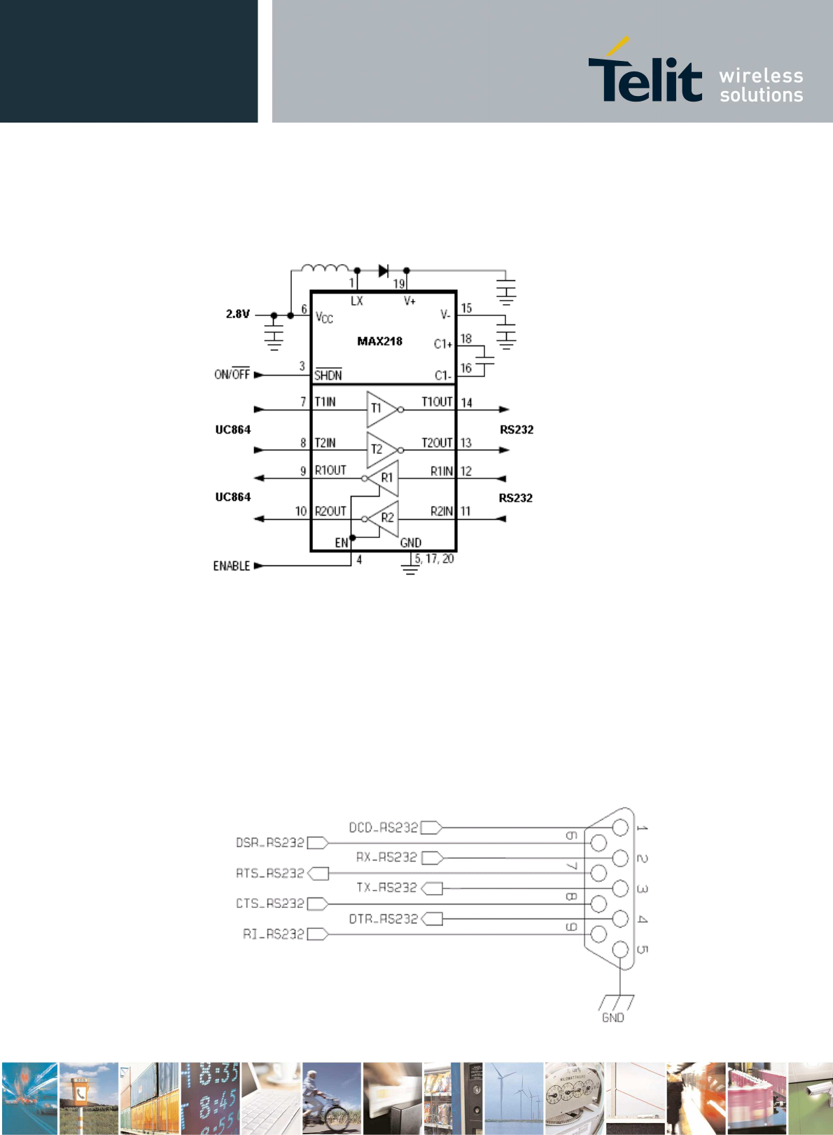
UC864-E-AUTO / AWS-AUTO Hardware User Guide
1vv0300795 Rev.11 – 2010/11/18
Reproduction forbidden without Telit Communications S.p.A’s. written authorization - All Rights Reserved. Page 45 of 78
Second solution could be done using a MAXIM transceiver (MAX218) In this case the
compliance with RS232 (+-5V) is possible.
Another level adapting method could be done using a standard RS232 Transceiver
(MAX3237EAI) adding some resistors to adapt the levels on the UC864 Input lines.
NOTE: In this case has to be taken in account the length of the lines on the
application to avoid problems in case of High-speed rates on RS232.
The RS232 serial port lines are usually connected to a DB9 connector with the
following layout: signal names and directions are named and defined from the DTE
point of view.
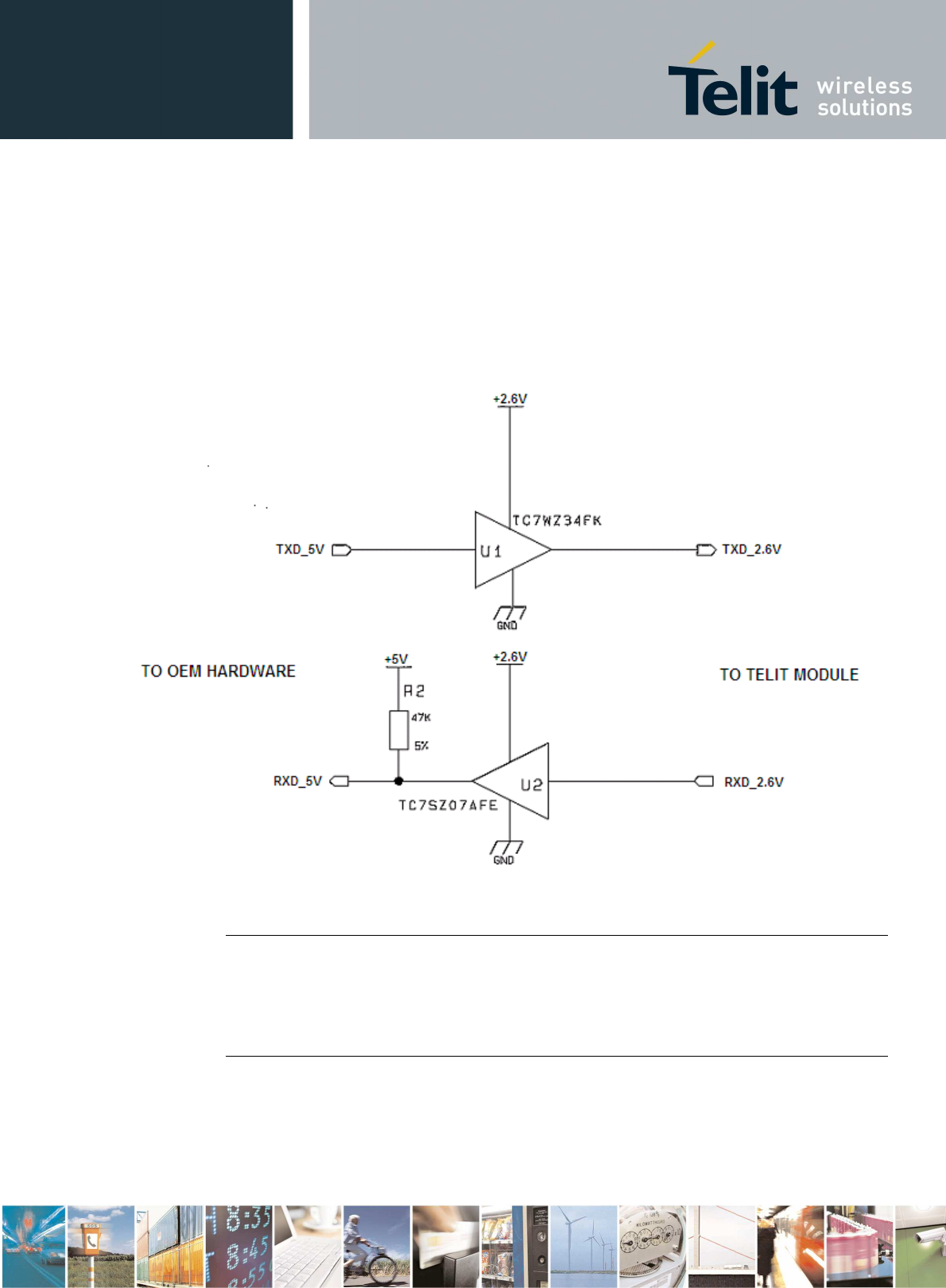
UC864-E-AUTO / AWS-AUTO Hardware User Guide
1vv0300795 Rev.11 – 2010/11/18
Reproduction forbidden without Telit Communications S.p.A’s. written authorization - All Rights Reserved. Page 46 of 78
10.3. 5V UART Level Transition
If the OEM application uses a microcontroller with a serial port (UART) that works at
a voltage different from 2.6 – 2.9V, then a circuitry has to adapt the different levels of
the two signal sets. As for the RS232 translation, there are a multitude of single chip
translators. For example a possible translator circuit for a 5V
TRANSMITTER/RECEIVER can be:
TIP:
TIP: TIP:
TIP:
This logic IC for the level translator and 2.6V pull-ups (not the 5V one) can be
powered directly from PWRMON line of UC864-E-AUTO / AWS-AUTO. Note that the
TC7SZ07AE has open drain output; therefore the resistor R2 is mandatory.

UC864-E-AUTO / AWS-AUTO Hardware User Guide
1vv0300795 Rev.11 – 2010/11/18
Reproduction forbidden without Telit Communications S.p.A’s. written authorization - All Rights Reserved. Page 47 of 78
A power source of the internal interface voltage corresponding to the 2.6V CMOS high
level is available at the VAUX pin on the connector.
A maximum of 9 resistors of 47 KΩ pull-up can be connected to the VAUX pin,
provided no other devices are connected to it and the pulled-up lines are UC864-E-
AUTO / AWS-AUTO input lines connected to open collector outputs in order to avoid
latch-up problems on UC864-E-AUTO / AWS-AUTO.
Careful approach is needed to avoid latch-up on UC864-E-AUTO / AWS-AUTO and the
use of this output line to power electronic devices must be avoided, especially for
devices that generate spikes and noise such as switching level translators, micro
controllers, failure in any of these condition can severely compromise the UC864-E-
AUTO / AWS-AUTO functionality.
NOTE:
NOTE: NOTE:
NOTE:
The input lines working at 2.6VCMOS can be pulled-up with 47KΩ resistors that can
be connected directly to the VAUX line. It is a must that they are connected as in this
example.
The preferable configuration is having external supply for the buffer.

UC864-E-AUTO / AWS-AUTO Hardware User Guide
1vv0300795 Rev.11 – 2010/11/18
Reproduction forbidden without Telit Communications S.p.A’s. written authorization - All Rights Reserved. Page 48 of 78
11. Audio Section Overview
Audio Section OverviewAudio Section Overview
Audio Section Overview
The
Baseband
chip was developed for the cellular phones, which needed two separated amplifiers
both in
RX
and in
TX
section.
A couple of amplifiers had to be used with internal audio transducers while the other couple of
amplifiers had to be used with external audio transducers.
To distinguish the schematic signals and the Software identifiers, two different definitions were
introduced, with the following meaning:
• internal audio transducers
HS/MT
HS/MTHS/MT
HS/MT
(from
H
HH
HandS
SS
Set
or
M
MM
MicroT
TT
Telephone
)
• external audio transducers
HF
HF HF
HF
(from HandsFree )
Actually the acronyms have not the original importance.
In other words this distinction is not necessary, being the performances between the two blocks like
the same.
Only if yhe customer needs higher output power to the speaker , he has a constraint. Otherwise the
choice could be done in order to overcome the PCB design difficulties.
For these reasons we have not changed the
HS
and
HF
acronyms, keeping them in the Software and
on the schematics.
The Base Band Chip of the UC864-E-AUTO / AWS-AUTO Telit Module maintains the same
architecture.
For more information refer to Telit document:
„
80000NT10025a UC864 Audio Settings Application Note
80000NT10025a UC864 Audio Settings Application Note80000NT10025a UC864 Audio Settings Application Note
80000NT10025a UC864 Audio Settings Application Note“
.
11.1.
Selecti
SelectiSelecti
Selection mode
on modeon mode
on mode
Only one block can be active at a time, and the activation of the requested audio path
is done via hardware by
AXE
AXEAXE
AXE
line or via software by
AT#CAP
AT#CAPAT#CAP
AT#CAP
command.
Moreover the
Sidetone
SidetoneSidetone
Sidetone
functionality could be implemented by the amplifier fitted between the
transmit path and the receive path, enabled at request in both modes
.
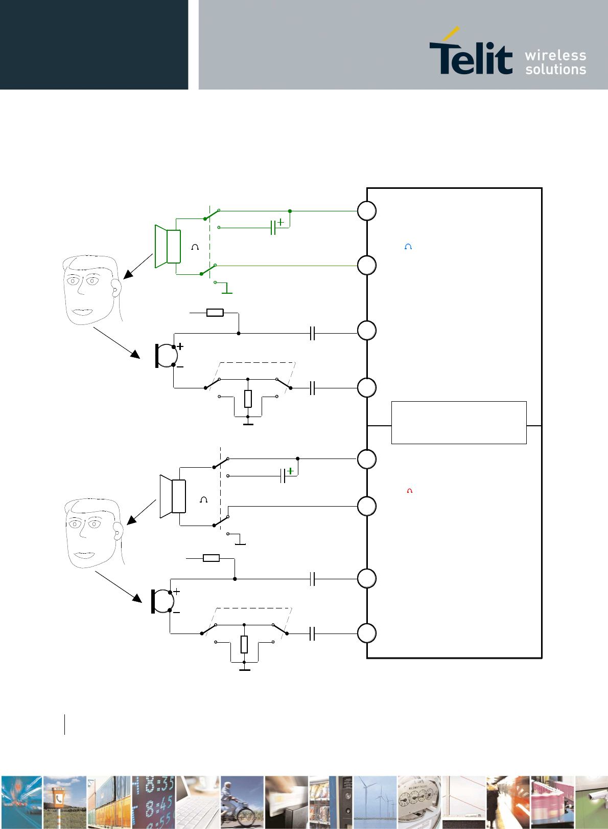
UC864-E-AUTO / AWS-AUTO Hardware User Guide
1vv0300795 Rev.11 – 2010/11/18
Reproduction forbidden without Telit Communications S.p.A’s. written authorization - All Rights Reserved. Page 49 of 78
UC864-E-AUTO / AWS-AUTO Audio Front End (
AFE
AFEAFE
AFE
)
100nF
100nF
Baseband
Audio Front End
Single ended
Balanced
Single ended
Bias
100nF
100nF
Single ended
Balanced
HPH_L (EAR_AMP2)
HPH_R (EAR_AMP3)
Differential Driver
32 Handset
Mono Differential
Headphone
32 Load
32
MIC1P
MIC1N
MIC2P
MIC2N
EAR1ONP (EAR_AMP1)
EAR1OP (EAR_AMP1)
uc864afe.skd
MIC 1
MIC 2
Ear_HF+
Ear_HF-
Mic_HF+
Mic_HF-
Ear MT+
Ear MT-
MIC MT+
MIC MT-
Single ended
Bias
Balanced
32
Balanced
UC864-E-AUTO / AWS-AUTO Hardware User Guide
1vv0300795 Rev.11 – 2010/11/18
Reproduction forbidden without Telit Communications S.p.A’s. written authorization - All Rights Reserved. Page 50 of 78
11.2. Electrical Characteristics
Electrical CharacteristicsElectrical Characteristics
Electrical Characteristics
11.2.1. Input Lines
(
((
(
MIC1 and MIC2
MIC1 and MIC2MIC1 and MIC2
MIC1 and MIC2
)
))
)
Characteristics
Line coupling AC (*)
Line type Balanced / Unbalanced
Coupling capacitor
>=
100nF
Differential input impedance 20Kohm
Differential input voltage
908mV
rms
(≤ 1290mV
rms
)
@ MicG=0dB
“Mic_MT” and “Mic_HF”
“Mic_MT” and “Mic_HF”“Mic_MT” and “Mic_HF”
“Mic_MT” and “Mic_HF” microphone paths
(*) WARNING :
(*) WARNING : (*) WARNING :
(*) WARNING : AC means that the signals from the microphone have to be
connected to input lines of the module through capacitors which value has to
be • 100nf. not respecting this constraint, the input stages will be damaged.
WARNING:
WARNING: WARNING:
WARNING: when
particular OEM application needs a
Single Ended Input
configuration, it is forbidden connecting the unused input directly to Ground,
but only through a 100nF capacitor. Don’t
forget that thus the useful input signal will be halved.
TIP:
TIP: TIP:
TIP: Being the microphone circuitry the more noise sensitive, its design and layout
must be realized with particular care. Both microphone paths are balanced and the
OEM circuitry must be balanced designed to reduce the common mode noise
typically generated on the ground plane. However
the customer can use the unbalanced circuitry for particular application.
.
UC864-E-AUTO / AWS-AUTO Hardware User Guide
1vv0300795 Rev.11 – 2010/11/18
Reproduction forbidden without Telit Communications S.p.A’s. written authorization - All Rights Reserved. Page 51 of 78
11.3. OUTPUT LINES
(
((
(
Speaker)
Speaker)Speaker)
Speaker)
We suggest driving the load differentially from both output drivers, thus the output
swing will double and the need for the output coupling capacitor avoided.
If a
particular OEM application needs a
Single Ended Output
configuration the output
power will be reduced four times.
The OEM circuitry shall be designed to reduce the common mode noise typically
generated on the ground plane and to get the maximum power output from the
device (low resistance tracks).
(*) WARNING:
(*) WARNING:(*) WARNING:
(*) WARNING:
Using single ended configuration, the unused output line must be left open.
Not respecting this constraint, the output stage will be damaged.
11.3.1. Output Lines Characteristics
Line coupling differential
single-ended
DC
AC
Output load impedance differential 32 ohm (≤ 26)
Differential output impedance ≤ 01 ohm @1.02kHz
Signal bandwidth 150 - 4000 Hz @ -3 dB
Differential output voltage (typ.) 1060 mV
rms
/32 ohm
Max Output Power 70mW @ 32 ohm
Max load capacitance 500pF
“
Ear_MT
Ear_MTEar_MT
Ear_MT
”
Output
OutputOutput
Output
(
EAR_AMP1
differential amplifier)
Line coupling differen
tial
single-ended
DC
AC
Output load impedance differential
single-
ended
32 ohm (≤ 26)
16 ohm (≤ 12)
S.E. output impedance ≤ 0,5 ohm @ 1.02kHz
signal bandwidth 150 - 4000 Hz @ -3 dB
Differential output voltage (typ.) 833 mV
rms
/32 ohm
Max Output Power @ 32 ohm
@ 16 ohm
44mW differential
22mW single-ended
Max load capacitance 1000pF
“
Ear_HF
Ear_HFEar_HF
Ear_HF
”
Output
OutputOutput
Output
(
EAR_AMP2 + EAR_AMP3
amplifiers)
UC864-E-AUTO / AWS-AUTO Hardware User Guide
1vv0300795 Rev.11 – 2010/11/18
Reproduction forbidden without Telit Communications S.p.A’s. written authorization - All Rights Reserved. Page 52 of 78
12. General Purpose I/O
General Purpose I/OGeneral Purpose I/O
General Purpose I/O
The general-purpose I/O pads can be configured to act in three different ways:
• input
• output
• alternate function (internally controlled)
Input pads can only be read and report the digital value (high or low) present on the
pad at the read time; output pads can only be written or queried and set the value of
the pad output; an alternate function pad is internally controlled by the UC864-E-
AUTO / AWS-AUTO firmware and acts depending on the function implemented.
The following GPIOs are available on the UC864-E-AUTO / AWS-AUTO:
PIN
PINPIN
PIN
Signal
SignalSignal
Signal
I/O
I/OI/O
I/O
Function
FunctionFunction
Function
Type
TypeType
Type
Drive
Drive Drive
Drive
strength
strengthstrength
strength
Default
Default Default
Default
State
StateState
State
ON_OFF
ON_OFF ON_OFF
ON_OFF
State
StateState
State
Reset
Reset Reset
Reset
State
StateState
State
Note
NoteNote
Note
70 GPIO_01
I/O
GPIO01 Configurable GPIO CMOS 2.6V 2mA INPUT LOW HIGH
74 GPIO_02
I/O
GPIO02 Configurable GPIO CMOS 2.6V 2mA INPUT LOW HIGH
66 GPIO_03
I/O
GPIO03 Configurable GPIO CMOS 2.6V 2mA INPUT LOW LOW
59 GPIO_04
I/O
GPIO04 Configurable GPIO CMOS 2.6V 2mA INPUT LOW LOW
Alternate
Function (RF
Transmission
Control)
78 GPIO_05
I/O
GPIO05 Configurable GPIO CMOS 2.6V 2mA INPUT LOW LOW
Alternate
Function
(RFTXMON)
68 GPIO_06
I/O
GPIO06 Configurable GPIO CMOS 2.6V 2mA INPUT LOW HIGH
Alternate
function
(ALARM)
73 GPIO_07
I/O
GPIO07 Configurable GPIO CMOS 2.6V 2mA INPUT LOW LOW
Alternate
function
(BUZZER)
67 GPIO_08
I/O
GPIO08 Configurable GPIO CMOS 2.6V 2mA INPUT LOW LOW
76 GPIO_09
I/O
GPIO09 Configurable GPIO CMOS 2.6V 2mA INPUT LOW HIGH
63 GPIO_10
I/O
GPIO10 Configurable GPIO CMOS 2.6V 2mA INPUT LOW LOW
57 GPIO_11
I/O
GPIO11 Configurable GPIO CMOS 2.6V 2mA INPUT LOW LOW
62 GPIO_12
I/O
GPIO12 Configurable GPIO CMOS 2.6V 2mA INPUT LOW HIGH
77 GPIO_13
I/O
GPIO13 Configurable GPIO CMOS 2.6V 2mA INPUT LOW LOW
60 TGPIO_1
4 I/O
GPIO14 Configurable GPIO CMOS 2.6V 2mA INPUT LOW HIGH
61 GPIO_15
I/O
GPIO15 Configurable GPIO CMOS 2.6V 2mA INPUT LOW HIGH
75 GPIO_16
I/O
GPIO16 Configurable GPIO CMOS 2.6V 2mA INPUT LOW HIGH
71 GPIO_17
I/O
GPIO17 Configurable GPIO CMOS 2.6V 2mA INPUT LOW LOW
65 GPIO_18
I/O
GPIO18 Configurable GPIO CMOS 2.6V 2mA INPUT LOW LOW

UC864-E-AUTO / AWS-AUTO Hardware User Guide
1vv0300795 Rev.11 – 2010/11/18
Reproduction forbidden without Telit Communications S.p.A’s. written authorization - All Rights Reserved. Page 53 of 78
56 GPIO_19
I/O
GPIO19 Configurable GPIO CMOS 2.6V 2mA INPUT LOW LOW
58 GPIO_20
I/O
GPIO20 Configurable GPIO CMOS 2.6V 2mA INPUT LOW LOW
72 GPIO_21
I/O
GPIO21 Configurable GPIO CMOS 2.6V 2mA INPUT HIGH HIGH
64 GPIO_22
I/O
GPIO22 Configurable GPIO CMOS 1.8V
(not 2.6V) 2mA INPUT LOW HIGH
Not all GPIO pads support all these three modes:
• GPIO4 supports all three modes and can be input, output, RF
Transmission Control (Alternate function)
• GPIO5 supports all three modes and can be input, output, RFTX monitor
output (Alternate function)
• GPIO6 supports all three modes and can be input, output, alarm output
(Alternate function)
• GPIO7 supports all three modes and can be input, output, buzzer output
(Alternate function)
Some alternate functions for UC864-E-AUTO / AWS-AUTO may be added if needed.
UC864-E-AUTO / AWS-AUTO Hardware User Guide
1vv0300795 Rev.11 – 2010/11/18
Reproduction forbidden without Telit Communications S.p.A’s. written authorization - All Rights Reserved. Page 54 of 78
12.1. Logic Level Specifications
Where not specifically stated, all the interface circuits work at 2.6V CMOS logic levels.
The following table shows the logic level specifications used in the UC864-E-AUTO /
AWS-AUTO interface circuits:
Absolute Maximum Ratings
Absolute Maximum Ratings Absolute Maximum Ratings
Absolute Maximum Ratings -
--
-Not Functional
Not FunctionalNot Functional
Not Functional
Parameter
ParameterParameter
Parameter
UC864
UC864UC864
UC864-
--
-E
EE
E-
--
-AUTO
AUTOAUTO
AUTO
/ AWS
/ AWS/ AWS
/ AWS-
--
-AUTO
AUTOAUTO
AUTO
Min
MinMin
Min
Max
MaxMax
Max
Input level on any
digital pin when on
-0.3V +3.0V
Input voltage on
analog pins when on
-0.3V +3.0 V
For 2.6V CMOS signals;
Operating Range
Operating Range Operating Range
Operating Range -
--
-
Interface levels
Interface levelsInterface levels
Interface levels
Level
LevelLevel
Level
UC864
UC864UC864
UC864-
--
-E
EE
E-
--
-AUTO
AUTOAUTO
AUTO
/ AWS
/ AWS/ AWS
/ AWS-
--
-AUTO
AUTOAUTO
AUTO
Min
MinMin
Min
Max
MaxMax
Max
Input high level 2.0V 2.9 V
Input low level -0.3V 0.6V
Output high level 2.15V 2.6V
Output low level 0V 0.45V
For 1.8V signals:
Operating Range
Operating Range Operating Range
Operating Range -
--
-
Interface levels (1.8V CMOS)
Interface levels (1.8V CMOS)Interface levels (1.8V CMOS)
Interface levels (1.8V CMOS)
Level
LevelLevel
Level
UC864
UC864UC864
UC864-
--
-E
EE
E-
--
-AUTO
AUTOAUTO
AUTO
/ AWS
/ AWS/ AWS
/ AWS-
--
-AUTO
AUTOAUTO
AUTO
Min
MinMin
Min
Max
MaxMax
Max
Input high level 1.5V 2.1V
Input low level -0.3V 0.5V
Output high level 1.35V 1.8V
Output low level 0V 0.45V

UC864-E-AUTO / AWS-AUTO Hardware User Guide
1vv0300795 Rev.11 – 2010/11/18
Reproduction forbidden without Telit Communications S.p.A’s. written authorization - All Rights Reserved. Page 55 of 78
12.2. Using a GPIO Pad as Input
The GPIO pads, when used as inputs, can be connected to a digital output of another
device and report its status, provided this device has interface levels compatible with
the 2.6V CMOS levels of the GPIO.
If the digital output of the device is connected with the GPIO input, the pad has
interface levels different from the 2.6V CMOS. It can be buffered with an open
collector transistor with a 47KΩ pull-up resistor to 2.6V.
12.3. Using a GPIO Pad as Output
The GPIO pads, when used as outputs, can drive 2.6V CMOS digital devices or
compatible hardware. When set as outputs, the pads have a push-pull output and
therefore the pull-up resistor may be omitted.

UC864-E-AUTO / AWS-AUTO Hardware User Guide
1vv0300795 Rev.11 – 2010/11/18
Reproduction forbidden without Telit Communications S.p.A’s. written authorization - All Rights Reserved. Page 56 of 78
12.4. Using the RF Transmission Control GPIO4
The GPIO4 pin, when configured as RF Transmission Control Input, permits to disable
the Transmitter when the GPIO is set to Low by the application. In the design it is
necessary to add a pull up resistor (47K to PWRMON).
12.5. Using the RFTXMON Output GPIO5
The GPIO5 pin, when configured as RFTXMON Output, is controlled by the UC864-E-
AUTO / AWS-AUTO module and will rise when the transmitter is active and fall after
the transmitter activity is completed.
For example, if a call is started, the line will be HIGH during all conversations and it
will be again LOW after hanged up.
The line rises up 300ms before first TX burst and will become again LOW from 500ms
to 1sec after last TX burst.
12.6. Using the Alarm Output GPIO6
The GPIO6 pad, when configured as Alarm Output, is controlled by the UC864-E-
AUTO / AWS-AUTO module and will rise when the alarm starts and fall after the
issue of a dedicated AT command.
This output can be used to power up the UC864-E-AUTO / AWS-AUTO controlling
microcontroller or application at the alarm time, giving you the possibility to program
a timely system wake-up to achieve some periodic actions and completely turn off
either the application or the UC864-E-AUTO / AWS-AUTO during sleep periods. This
will dramatically reduce the sleep consumption to few µA.
In battery-powered devices this feature will greatly improve the autonomy of the
device.
NOTE:
NOTE: NOTE:
NOTE:
During RESET the line is set to HIGH logic level.
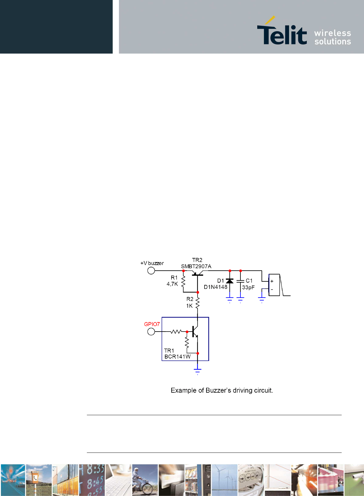
UC864-E-AUTO / AWS-AUTO Hardware User Guide
1vv0300795 Rev.11 – 2010/11/18
Reproduction forbidden without Telit Communications S.p.A’s. written authorization - All Rights Reserved. Page 57 of 78
12.7. Using the Buzzer Output GPIO7
As Alternate Function, the GPIO7 is controlled by the firmware that depends on the
function implemented internally.
This setup places always the GPIO7 pin in OUTPUT direction and the corresponding
function must be activated properly by AT#SRP command (refer to AT commands
specification).
Also in this case, the
dummy value
for the pin state can be both “0” or “1”.
send the command AT#GPIO=7, 1, 2<cr>:
wait for response OK
send the command AT#SRP=3
The GPIO7 pin will be set as
Alternate Function
pin with its dummy logic status set to
HIGH
value.
The "Alternate function” permits your application to easily implement Buzzer feature
with some small hardware extension of your application as shown in the next sample
figure.
NOTE:
NOTE: NOTE:
NOTE:
To correctly drive a buzzer, a driver must be provided. its characteristics depend on
the buzzer. Refer to your buzzer vendor.
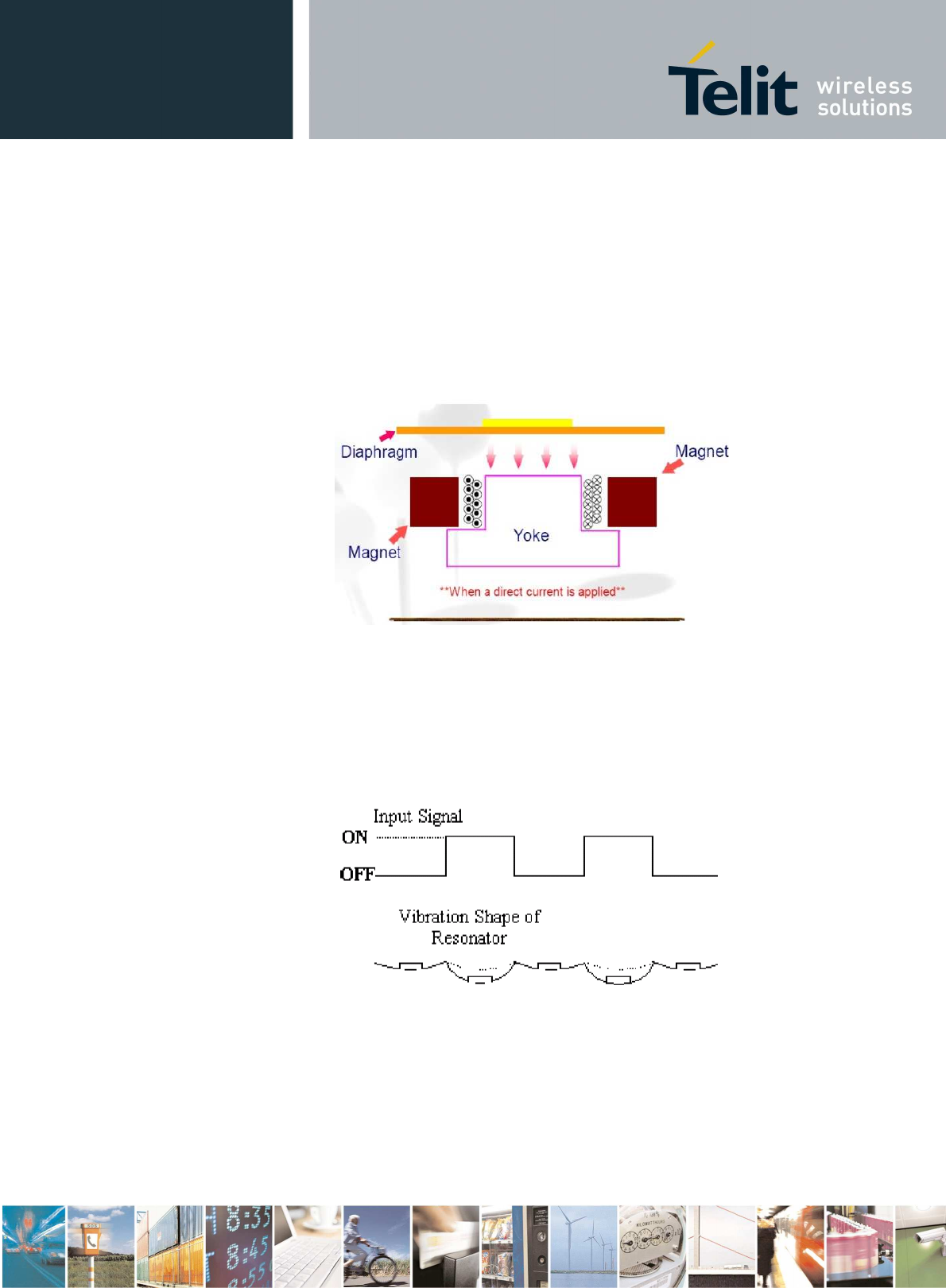
UC864-E-AUTO / AWS-AUTO Hardware User Guide
1vv0300795 Rev.11 – 2010/11/18
Reproduction forbidden without Telit Communications S.p.A’s. written authorization - All Rights Reserved. Page 58 of 78
12.8. Magnetic Buzzer Concepts
12.8.1. Short Description
A magnetic Buzzer is a sound-generating device with a coil located in the magnetic
circuit consisting of a permanent magnet, an iron core, a high permeable metal disk
and a vibrating diaphragm.
Drawing of the Magnetic Buzzer.
The disk and diaphragm are attracted to the core by the magnetic field. When an
oscillating signal is moved through the coil, it produces a fluctuating magnetic field,
which vibrates the diaphragm at a frequency of the drive signal. Thus the sound is
produced as relative to the frequency applied.
Diaphragm movement.

UC864-E-AUTO / AWS-AUTO Hardware User Guide
1vv0300795 Rev.11 – 2010/11/18
Reproduction forbidden without Telit Communications S.p.A’s. written authorization - All Rights Reserved. Page 59 of 78
12.8.2. Frequency Behavior
The frequency behavior represents the effectiveness of the reproduction of the
applied signals. Because its performance is related to a square driving waveform
(whose amplitude varies from 0V to Vpp), if you modify the waveform (e.g. from
square to sinus) the frequency response will change.
12.8.3. Power Supply Influence
After applying a signal with a different amplitude from suggested by the
manufacturer, a performance change will follow, according to the rule “
if resonance
frequency f
ff
f
o
oo
o
increases, amplitude decreases
”.
Because resonance frequency depends on acoustic design and lowering the
amplitude of the driving signal, the response bandwidth tends to become narrow, and
vice versa.
Summarizing:
Vpp
↑
f
ff
f
o
o o
o
↓
Vpp
f
ff
f
o
o o
o
↑
The risk is that the
f
ff
f
o
o o
o
could easily fall outside of new bandwidth; consequently the
SPL could be much lower than the expected.
12.8.4. Working Current Influence
In the component data sheet you will find the value of MAX CURRENT: this
represents the maximum average current that can flow at nominal voltage without
current limitation.
In other words it is not the peak current, which could be twice or three times higher.
If driving circuitry does not support these peak values, the SPL will never reach the
declared level or the oscillations will stop.
WARNING
WARNINGWARNING
WARNING:
It is very important to respect the sense of the applied voltage: never apply to the "-"
pin a voltage more positive than "+" pin. If this happens, the diaphragm vibrates in
the opposite sense with a high probability to be expelled from its physical position.
This damages the device permanently.
UC864-E-AUTO / AWS-AUTO Hardware User Guide
1vv0300795 Rev.11 – 2010/11/18
Reproduction forbidden without Telit Communications S.p.A’s. written authorization - All Rights Reserved. Page 60 of 78
12.9. Using the Temperature Monitor Function
12.9.1. Short Description
The Temperature Monitor is a function of the module that permits to control its
internal temperature and if properly set (see the #TEMPMON command on AT
Interface guide) it raises to High Logic level a GPIO when the maximum temperature
is reached.
12.9.2. Allowed GPIO
The AT#TEMPMON set command could be used with one of the following GPIO:
Signal
SignalSignal
Signal
Function
FunctionFunction
Function
Type
TypeType
Type
Drive
Drive Drive
Drive
strength
strengthstrength
strength
Note
NoteNote
Note
GPIO_01 GPIO01 Configurable GPIO CMOS 2.6V 2mA
GPIO_03 GPIO03 Configurable GPIO CMOS 2.6V 2mA
GPIO_08 GPIO08 Configurable GPIO CMOS 2.6V 2mA
GPIO_09 GPIO09 Configurable GPIO CMOS 2.6V 2mA
GPIO_10 GPIO10 Configurable GPIO CMOS 2.6V 2mA
GPIO_11 GPIO11 Configurable GPIO CMOS 2.6V 2mA
GPIO_12 GPIO12 Configurable GPIO CMOS 2.6V 2mA
GPIO_13 GPIO13 Configurable GPIO CMOS 2.6V 2mA
GPIO_14 GPIO14 Configurable GPIO CMOS 2.6V 2mA
GPIO_15 GPIO15 Configurable GPIO CMOS 2.6V 2mA
GPIO_16 GPIO16 Configurable GPIO CMOS 2.6V 2mA
GPIO_17 GPIO17 Configurable GPIO CMOS 2.6V 2mA
GPIO_18 GPIO18 Configurable GPIO CMOS 2.6V 2mA
GPIO_19 GPIO19 Configurable GPIO CMOS 2.6V 2mA
GPIO_20 GPIO20 Configurable GPIO CMOS 2.6V 2mA
GPIO_22 GPIO22 Configurable GPIO CMOS 1.8V (not
2.6V) 2mA
UC864-E-AUTO / AWS-AUTO Hardware User Guide
1vv0300795 Rev.11 – 2010/11/18
Reproduction forbidden without Telit Communications S.p.A’s. written authorization - All Rights Reserved. Page 61 of 78
The set command could be used also with one of the following GPIO but in that case
the alternate function is not usable:
Sign
SignSign
Signal
alal
al
Function
FunctionFunction
Function
Type
TypeType
Type
Drive
Drive Drive
Drive
strength
strengthstrength
strength
Note
NoteNote
Note
GPIO_02 GPIO02 Configurable GPIO CMOS 2.6V 2mA Alternate
function(JDR)
GPIO_04 GPIO04 Configurable GPIO CMOS 2.6V 2mA Alternate Function (RF
Transmission Control)
GPIO_05 GPIO05 Configurable GPIO CMOS 2.6V 2mA Alternate Function
(RFTXMON)
GPIO_07 GPIO07 Configurable GPIO CMOS 2.6V 2mA Alternate function
(BUZZER)
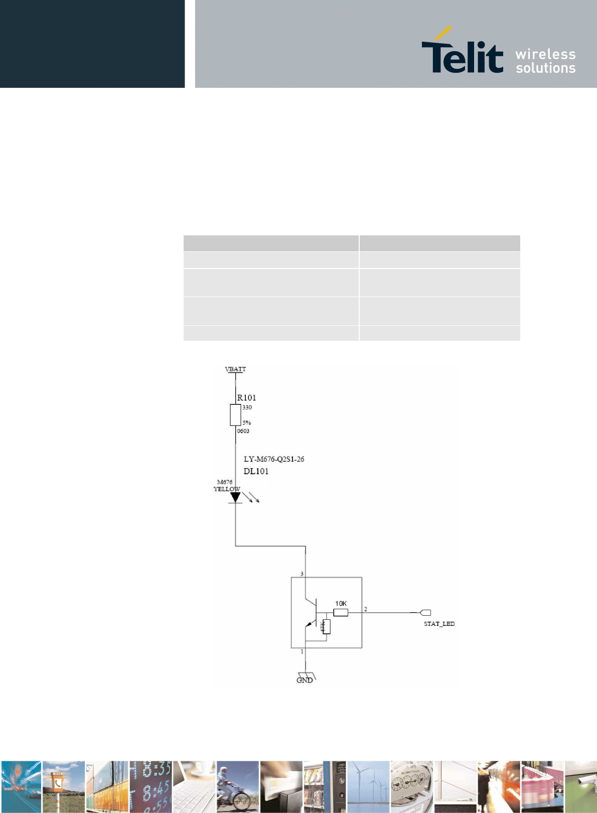
UC864-E-AUTO / AWS-AUTO Hardware User Guide
1vv0300795 Rev.11 – 2010/11/18
Reproduction forbidden without Telit Communications S.p.A’s. written authorization - All Rights Reserved. Page 62 of 78
12.10. Indication of Network Service Availability
The STAT_LED pin status shows information on the network service availability and
Call status. In the UC864-E-AUTO / AWS-AUTO modules, the STAT_LED usually
needs an external transistor to drive an external LED. Because of the above, the
status indicated in the following table is reversed with respect to the pin status:
LED status
LED statusLED status
LED status
Device
DeviceDevice
Device Status
StatusStatus
Status
Permanently off Device off
Fast blinking
(Period 1s, Ton 0,5s)
Net search / Not registered /
turning off
Slow blinking
(Period 3s, Ton 0,3s)
Registered full service
Permanently on a call is active
UC864-E-AUTO / AWS-AUTO Hardware User Guide
1vv0300795 Rev.11 – 2010/11/18
Reproduction forbidden without Telit Communications S.p.A’s. written authorization - All Rights Reserved. Page 63 of 78
12.11. RTC Bypass Out
The VRTC pin brings out the Real Time Clock supply, which is separate from the rest
of the digital part, allowing having only RTC going on when all the other parts of the
device are off. To this power output a backup capacitor can be added in order to
increase the RTC autonomy during power off of the battery.
NOTE: NO devices must be powered from this pin.
12.12. VAUX1 Power Output
A regulated power supply output is provided in order to supply small devices from
the module. This output is active when the module is ON and goes OFF when the
module is shut down. The operating range characteristics of the supply are:
Operating Range
Operating Range Operating Range
Operating Range –
VAUX1 power supply
VAUX1 power supplyVAUX1 power supply
VAUX1 power supply
Min
MinMin
Min
Typical
TypicalTypical
Typical
Max
MaxMax
Max
Output voltage
Output voltageOutput voltage
Output voltage
2.6V 2.65V 2.7V
Output current
Output currentOutput current
Output current
100mA
Output bypass capacitor
Output bypass capacitorOutput bypass capacitor
Output bypass capacitor
(Inside the module)
(Inside the module)(Inside the module)
(Inside the module)
2.2µF

UC864-E-AUTO / AWS-AUTO Hardware User Guide
1vv0300795 Rev.11 – 2010/11/18
Reproduction forbidden without Telit Communications S.p.A’s. written authorization - All Rights Reserved. Page 64 of 78
13. DAC and ADC section
DAC and ADC sectionDAC and ADC section
DAC and ADC section
13.1. DAC Converter
13.1.1. Description
The UC864-E-AUTO / AWS-AUTO module provides a Digital to Analog Converter. The
signal (named DAC_OUT) is available on pin 40 of the UC864-E-AUTO / AWS-AUTO
module and on pin 17 of PL102 on EVK2 Board (KS101C).
The on board DAC is a 16-bit converter, able to generate an analogue value based on
a specific input in the range from 0 up to 65535 but recalibrated in the range from 0
to 1023. However, an external low-pass filter is necessary.
Min
MinMin
Min
Max
MaxMax
Max
Units
UnitsUnits
Units
Voltage range (filtered) 0 2.6 Volt
Range 0 1023 Steps
The precision is 1023 steps, so if we consider that the maximum voltage is 2V, the
integrated voltage could be calculated with the following formula:
Integrated output voltage = 2 * value / 1023
DAC_OUT line must be integrated (for example with a low band pass filter) in order to
obtain an analog voltage.
13.1.2. Enabling DAC
An AT command is available to use the DAC function. The command
is:AT#DAC[=<enable>[,<value>]]
<value> - scale factor of the integrated output voltage (0..1023 - 10 bit precision)
it must be present if <enable>=1
Refer to SW User Guide or AT Commands Reference Guide for the full description of
this function.
NOTE:
NOTE: NOTE:
NOTE:
The DAC frequency is selected internally. D/A converter must not be used during
POWERSAVING.
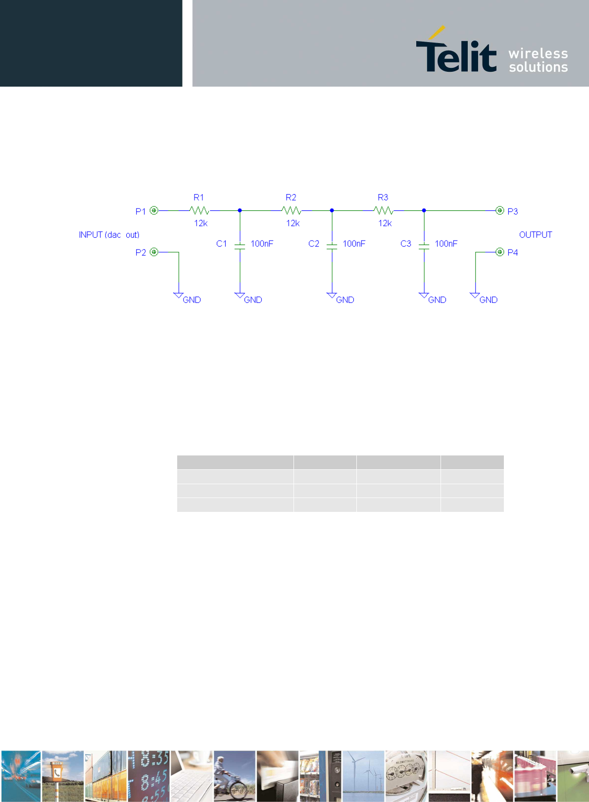
UC864-E-AUTO / AWS-AUTO Hardware User Guide
1vv0300795 Rev.11 – 2010/11/18
Reproduction forbidden without Telit Communications S.p.A’s. written authorization - All Rights Reserved. Page 65 of 78
13.1.3. Low Pass Filter Example
13.2. ADC Converter
13.2.1. Description
The on board ADCs are 8-bit converters. They are able to read a voltage level in the
range of 0-2 volts applied on the ADC pin input and store and convert it into 8 bit
word.
Min
MinMin
Min
Max
MaxMax
Max
Units
UnitsUnits
Units
Input Voltage range 0 2 Volt
AD conversion - 8 bits
Resolution - < 10.2 mV
The UC864-E-AUTO / AWS-AUTO module provides 3 Analog to Digital Converters.
The input lines are:
ADC_IN1 available on Pin 37 and Pin 19 of PL102 on EVK2 Interface.
ADC_IN2 available on Pin 38 and Pin 20 of PL102 on EVK2 Interface.
ADC_IN3 available on Pin 39 and Pin 21 of PL102 on EVK2 Interface.
13.2.2. Using ADC Converter
An AT command is available to use the ADC function.
The command is AT#ADC=1,2 The read value is expressed in mV
Refer to SW User Guide or AT Commands Reference Guide for the full description of
this function.
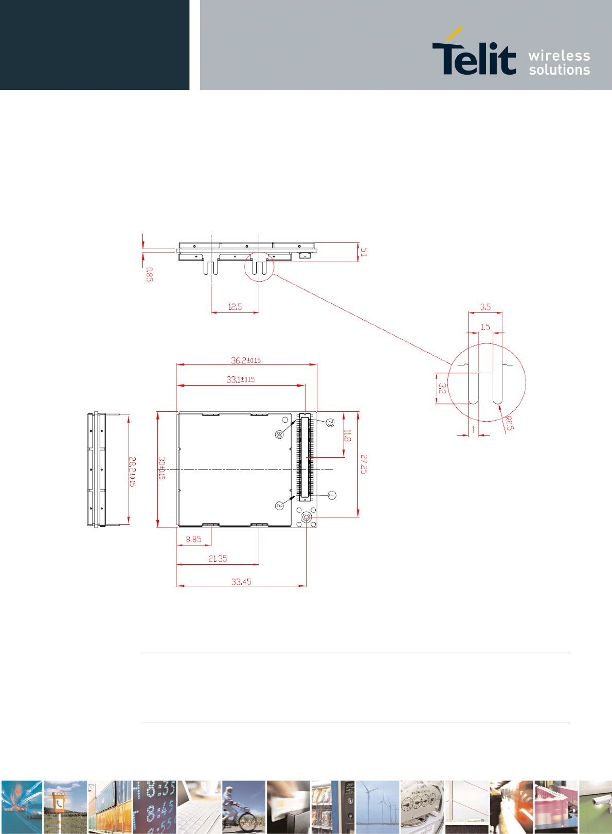
UC864-E-AUTO / AWS-AUTO Hardware User Guide
1vv0300795 Rev.11 – 2010/11/18
Reproduction forbidden without Telit Communications S.p.A’s. written authorization - All Rights Reserved. Page 66 of 78
14. Mounting the module on your board
Mounting the module on your boardMounting the module on your board
Mounting the module on your board
The position of the Molex board-to-board connector and pin 1 are shown in the
following picture.
NOTE:
NOTE: NOTE:
NOTE:
The Metal taps present on UC864-E-AUTO / AWS-AUTO must be connected to GND
This module could not be processed with a reflow
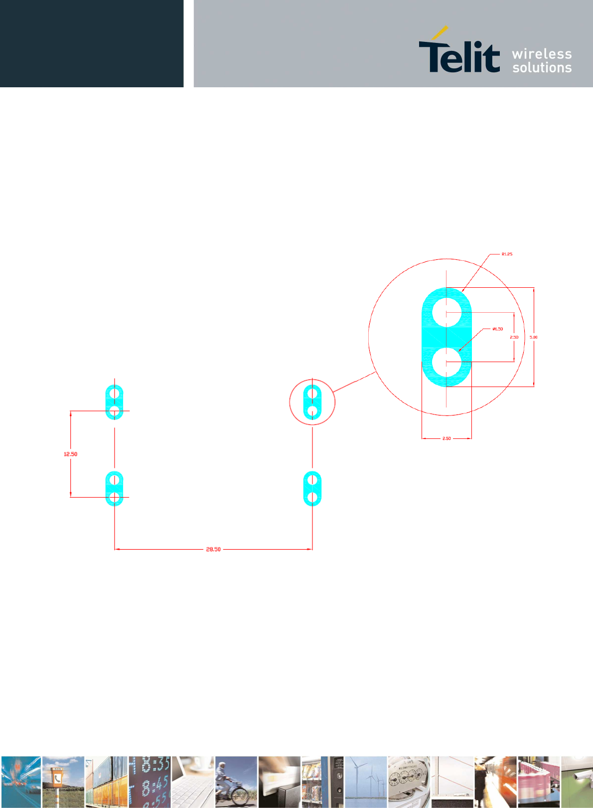
UC864-E-AUTO / AWS-AUTO Hardware User Guide
1vv0300795 Rev.11 – 2010/11/18
Reproduction forbidden without Telit Communications S.p.A’s. written authorization - All Rights Reserved. Page 67 of 78
14.1. Application PCB Layout
To obtain the best thermal dissipation it is suggested to design the host PCB as in the
below image where a Ground area has been created below the module.
Bottom side
Top View
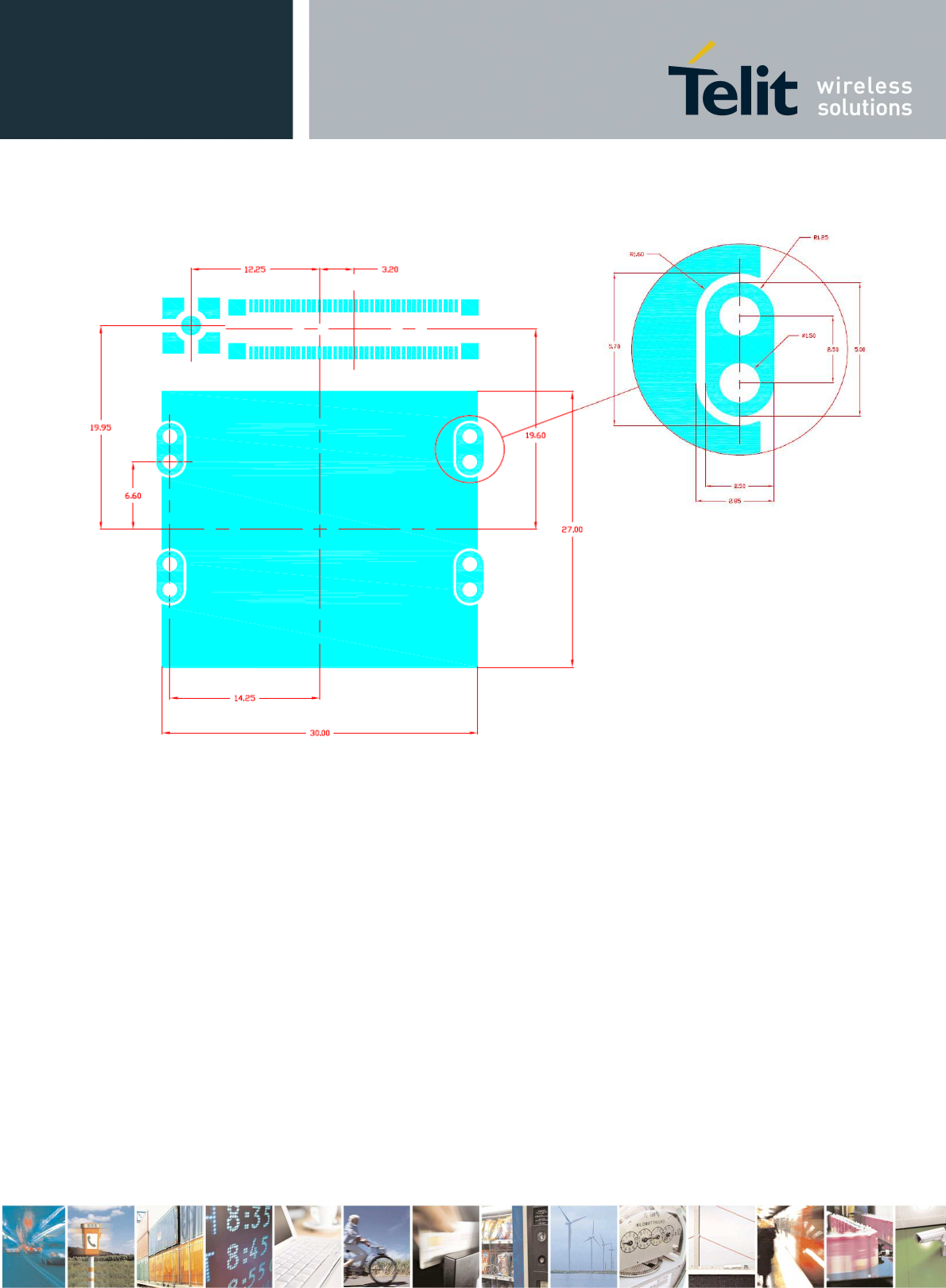
UC864-E-AUTO / AWS-AUTO Hardware User Guide
1vv0300795 Rev.11 – 2010/11/18
Reproduction forbidden without Telit Communications S.p.A’s. written authorization - All Rights Reserved. Page 68 of 78
Top side
Top View

UC864-E-AUTO / AWS-AUTO Hardware User Guide
1vv0300795 Rev.11 – 2010/11/18
Reproduction forbidden without Telit Communications S.p.A’s. written authorization - All Rights Reserved. Page 69 of 78
14.2. Clearance Area
14.3. Thermal Dissipation
To permit a better thermal dissipation it is suggested to use a Thermal conductive
material between the module and the application PCB.
Suggested types are Bergquist (Two parts) GAP filler 3500 or GAP Filler 1500
Clearance area for SMT
Components

UC864-E-AUTO / AWS-AUTO Hardware User Guide
1vv0300795 Rev.11 – 2010/11/18
Reproduction forbidden without Telit Communications S.p.A’s. written authorization - All Rights Reserved. Page 70 of 78
14.4. Module Soldering
The module could be soldered on the application in different kind of ways. Typical processes are
follows:
• Manual Soldering
• Automatic Selective soldering
• Wave soldering
We suggest respecting necessary Clearance area in the design to permit a proper soldering process
as shown in previous chapter.

UC864-E-AUTO / AWS-AUTO Hardware User Guide
1vv0300795 Rev.11 – 2010/11/18
Reproduction forbidden without Telit Communications S.p.A’s. written authorization - All Rights Reserved. Page 71 of 78
15. Application guide
Application guideApplication guide
Application guide
15.1. Debug of the UC864-E-AUTO /
AWS-AUTO in production
To test and debug the mounting of UC864-E-AUTO / AWS-AUTO, we strongly
recommend to foresee test pads on the host PCB, in order to check the connection
between the UC864-E-AUTO / AWS-AUTO itself and the application and to test the
performance of the module connecting it with an external computer. Depending on
the customer application, these pads include, but are not limited to the following
signals:
• TXD
• RXD
• ON/OFF
• RESET
• GND
• VBATT
• TX_TRACE
• RX_TRACE
• PWRMON
• USB_VBUS
• USB_D+
• USB_D-

UC864-E-AUTO / AWS-AUTO Hardware User Guide
1vv0300795 Rev.11 – 2010/11/18
Reproduction forbidden without Telit Communications S.p.A’s. written authorization - All Rights Reserved. Page 72 of 78
15.2. Bypass capacitor on Power supplies
When a sudden voltage is asserted to or cut from the power supplies, the steep
transition makes some reactions such as the overshoot and undershoot.
This abrupt voltage transition can affect the device not to work or make it
malfunction.
The bypass capacitors are needed to alleviate this behavior and it can be affected
differently according to the various applications. The customers have to pay special
attention to this when they design their application board..
The length and width of the power lines need to be considered carefully and the
capacitance of the capacitors need to be selected accordingly.
The capacitor will also avoid the ripple of the power supplies and the switching noise
caused in TDMA system like GSM.
Specially the suitable bypass capacitor must be mounted on the Vbatt (Pin 1,2,3,4)
and USB_VBUS (Pin 48) lines in the application board.
The recommended values can be presented as;
100uF for Vbatt
10uF for USB_VBUS
But the customers still have to consider that the capacitance mainly depends on the
conditions of their application board.
Generally more capacitance is required as the power line is longer.
15.3. SIM interface
The resistor value on SIMIO pulled up to SIMVCC should be defined accordingly in
order to be compliant to 3GPP specification.
6.8kohm can be recommended but it may depend on the application design..
Refer to the following document for the detail;
Telit_SIM_interface_and ESD_protection_Application_note_r1
UC864-E-AUTO / AWS-AUTO Hardware User Guide
1vv0300795 Rev.11 – 2010/11/18
Reproduction forbidden without Telit Communications S.p.A’s. written authorization - All Rights Reserved. Page 73 of 78
15.4. EMC recommendations
UC864-E-AUTO / AWS-AUTO signals are provided by some EMC protections. In any
case the accepted levels are different on the pins. The characteristics are described
in the following Table:
Pin
PinPin
Pin
Signal
SignalSignal
Signal
I/O
I/OI/O
I/O
Function
FunctionFunction
Function
Contact
ContactContact
Contact
Air
AirAir
Air
Power Supply
Power SupplyPower Supply
Power Supply
1,2,3,4
1,2,3,41,2,3,4
1,2,3,4
VBATT - Main power supply
± 8KV
± 15KV
SIM Card Interface
SIM Card InterfaceSIM Card Interface
SIM Card Interface
18
1818
18
SIMVCC - External SIM signal – Power supply for the SIM
± 8KV
± 15KV
19
1919
19
SIMRST O External SIM signal – Reset
± 8KV
± 15KV
20
2020
20
SIMIO I/O External SIM signal - Data I/O
± 8KV
± 15KV
22
2222
22
SIMCLK O External SIM signal – Clock
± 8KV
± 15KV
Miscellaneous Fun
Miscellaneous FunMiscellaneous Fun
Miscellaneous Functions
ctionsctions
ctions
35
3535
35
USB_ID AI
Analog input used to sense whether a peripheral device is
connected
± 8KV
± 15KV
Miscellaneous Functions
Miscellaneous FunctionsMiscellaneous Functions
Miscellaneous Functions
48
4848
48
USB_VBUS AI Power supply for the internal USB transceiver.
± 8KV
± 15KV
50
5050
50
VAUX1 - Power output for external accessories
± 8KV
± 15KV
51, 52
51, 5251, 52
51, 52
CHARGE AI Charger input
± 8KV
± 15KV
53
5353
53
ON/OFF I Input command for switching power ON or OFF (toggle command).
± 8KV
± 15KV
54
5454
54
RESET I Reset input
± 8KV
± 15KV
55
5555
55
VRTC AO Power supply for RTC block
± 8KV
± 15KV
Antenna
AntennaAntenna
Antenna
PAD
PADPAD
PAD
Antenna Pad AI Antenna pad for Rosenberger connector
± 8KV
± 15KV
All other pins have the following characteristics:
HBM JESD22-A114-B ± 2000 V
CDM JESD22-C101-C ± 500 V
The Board to Board connector has to be considered as NO TOUCH area.
Appropriate Series resistors has to be considered to protect the input lines from overvoltage.
UC864-E-AUTO / AWS-AUTO Hardware User Guide
1vv0300795 Rev.11 – 2010/11/18
Reproduction forbidden without Telit Communications S.p.A’s. written authorization - All Rights Reserved. Page 74 of 78
16. Pac
PacPac
Pack
kk
king system
ing systeming system
ing system
The Telit UC864-E-AUTO / AWS-AUTO is packaged on trays. Each tray contains 20
pieces with the following dimensions:
NOTE:
NOTE: NOTE:
NOTE:
Trays can withstand the maximum temperature of 65° C.

UC864-E-AUTO / AWS-AUTO Hardware User Guide
1vv0300795 Rev.11 – 2010/11/18
Reproduction forbidden without Telit Communications S.p.A’s. written authorization - All Rights Reserved. Page 75 of 78
17. Conformity Assessment Issues
Conformity Assessment IssuesConformity Assessment Issues
Conformity Assessment Issues
The Telit UC864
UC864UC864
UC864-
--
-E
EE
E-
--
-AUTO
AUTOAUTO
AUTO module has been assessed in order to satisfy the essential requirements
of the R&TTE Directive 1999/05/EC (Radio Equipment & Telecommunications Terminal Equipments)
to demonstrate the conformity against the harmonized standards with the final involvement of a
Notified Body.
If the module is installed in conformance to the Telit installation manuals, no further evaluation
under Article 3.2
Article 3.2Article 3.2
Article 3.2 of the R&TTE Directive and do not require further involvement of a R&TTE
Directive Notified Body for the final product.
In all other cases, or if the manufacturer of the final product is in doubt, then the equipment
integrating the radio module must be assessed against Article 3.2
Article 3.2Article 3.2
Article 3.2 of the R&TTE Directive.
In all cases the assessment of the final product must be made against the Essential requirements
of the R&TTE Directive Articles 3.1(a)
Articles 3.1(a)Articles 3.1(a)
Articles 3.1(a) and (b)
(b)(b)
(b), Safety and EMC respectively, and any relevant Article
3.3 requirements.
This Hardware User Guide contains all the information you may need for developing a product
meeting the R&TTE Directive.
The Telit UC864
UC864UC864
UC864-
--
-AWS
AWSAWS
AWS-
--
-AUTO
AUTOAUTO
AUTO module is FCC Approved as module to be installed in other devices.
This device is to be used only for fixed and mobile applications. If the final product after integration
is intended for portable use, a new application and FCC is required.
The UC864
UC864UC864
UC864-
--
-AWS
AWSAWS
AWS-
--
-AUTO
AUTOAUTO
AUTO Module
ModuleModule
Module is conforming to the following US Directives:
• Use of RF Spectrum. Standards: FCC 47 Part 22 (GSM 850), Part 24 (PCS 1900) and Part 27 (FDD
IV)
• EMC (Electromagnetic Compatibility). Standards: FCC47 Part 15
This device complies with Part 15 of the FCC Rules. Operation is subject to the following two
conditions:
(1) this device may not cause harmful interference, and
(2) this device must accept any interference received, including interference that may cause
undesired operation.

UC864-E-AUTO / AWS-AUTO Hardware User Guide
1vv0300795 Rev.11 – 2010/11/18
Reproduction forbidden without Telit Communications S.p.A’s. written authorization - All Rights Reserved. Page 76 of 78
To meet the FCC's RF exposure rules and regulations:
• The system antenna(s) used for this transmitter must be installed to provide a separation
distance of at least 20 cm from all the persons and must not be co-located or operating in
conjunction with any other antenna or transmitter.
•
The system antenna(s) used for this module must not exceed 7.18 dBi (GSM 850), 2.78 dBi (PCS 1900)
and 1.43 dBi (FDD IV) for mobile and fixed or mobile operating configurations.
• Users and installers must be provided with antenna installation instructions and transmitter
operating conditions for satisfying RF exposure compliance.
Manufacturers of mobile, fixed or portable devices incorporating this module are advised to clarify
any regulatory questions and to have their complete product tested and approved for FCC
compliance.
The FCC requires that you be notified that any changes or modifications made to the UC864-AWS-
AUTO module that are not expressly approved by Telit Communications S.p.A. may void your
authority to operate the equipment.

UC864-E-AUTO / AWS-AUTO Hardware User Guide
1vv0300795 Rev.11 – 2010/11/18
Reproduction forbidden without Telit Communications S.p.A’s. written authorization - All Rights Reserved. Page 77 of 78
18. Safety R
Safety RSafety R
Safety Recommendations
ecommendationsecommendations
ecommendations
Read carefully!
Be sure about that the use of this product is allowed in your country and in the environment
required. The use of this product may be dangerous and has to be avoided in the following
areas:
• Where it can interfere with other electronic devices in environments such as
hospitals, airports, aircrafts, etc.
• Where there is risk of explosion such as gasoline stations, oil refineries, etc.
It is responsibility of the user to enforce the country regulation and the specific environment
regulation.
Do not disassemble the product; any mark of tampering will compromise the warranty validity.
We recommend following the instructions of the hardware user guides for a correct wiring of
the product. The product has to be supplied with a stabilized voltage source and the wiring
has to be conforming to the security and fire prevention regulations.
The product has to be handled with care, avoiding any contact with the pins because
electrostatic discharges may damage the product itself. Same cautions have to be taken for
the SIM, checking carefully the instruction for its use. Do not insert or remove the SIM when
the product is in power saving mode.
The system integrator is responsible of the functioning of the final product; therefore, care
has to be taken to the external components of the module, as well as of any project or
installation issue, because the risk of disturbing the GSM network or external devices or
having impact on the security. Should there be any doubt, please refer to the technical
documentation and the regulations in force.
Every module has to be equipped with a proper antenna with specific characteristics. The
antenna has to be installed with care in order to avoid any interference with other electronic
devices and has to be installed with the guarantee of a minimum 20 cm distance from the
body. In case of this requirement cannot be satisfied, the system integrator has to assess the
final product against the SAR regulation.
The European Community provides some Directives for the electronic equipments introduced
on the market. All the relevant information are available on the European Community
website:
http://europa.eu.int/comm/enterprise/rtte/dir99-5.htm
The text of the Directive 99/05 regarding telecommunication equipments is available, while
the applicable Directives (Low Voltage and EMC) are available at:
http://europa.eu.int/comm/enterprise/rtte/dir99-5.htm
UC864-E-AUTO / AWS-AUTO Hardware User Guide
1vv0300795 Rev.11 – 2010/11/18
Reproduction forbidden without Telit Communications S.p.A’s. written authorization - All Rights Reserved. Page 78 of 78
19. Document Change Log
Document Change LogDocument Change Log
Document Change Log
R
RR
R
R
RR
R
e
ee
e
e
ee
e
v
vv
v
v
vv
v
i
ii
i
i
ii
i
s
ss
s
s
ss
s
i
ii
i
i
ii
i
o
oo
o
o
oo
o
n
nn
n
n
nn
n
D
DD
D
D
DD
D
a
aa
a
a
aa
a
t
tt
t
t
tt
t
e
ee
e
e
ee
e
C
CC
C
C
CC
C
h
hh
h
h
hh
h
a
aa
a
a
aa
a
n
nn
n
n
nn
n
g
gg
g
g
gg
g
e
ee
e
e
ee
e
s
ss
s
s
ss
s
Rev.0 2008/10/22 Initial release
Rev.1 2009/04/02 Updated with new HW design of solder tags, added info on Pull up/down
values on I/O lines, added soldering info
Updated ESD data
Rev.2 2009/06/11
Updated with new Module Drawings, updated ESD data, pinout.
Rev.3 2009/07/08 Updated Drawings of the module
Updated Turning ON/OFF
Updated Power supply : Consumption for GPRS/EDGE Class 12
Updated Audio section
Added Buzzer concept
Updated Application guide
Updated Packaging Tray dimensions
Rev.4 2009/10/29 Updated On Off timings
Rev.5 2009/11/09 Corrected Note on Chapter 4.2 (was related to E version and not to E-
AUTO)
Rev. 6 2010/05/06 Updated digital operating levels; added UC864-AWS-AUTO product
Updated GSM/WCDMA Antenna requirement
Updated 9 USB Port
Rev. 7 2010/07/02 Added section on Temperature Ranges
Rev. 8 2010/10/14 Conformity Assessment Issues section updated
Rev. 9 2010/10/25 Conformity Assessment Issues section updated
Rev. 10 2010/11/10 Section 7.1 and Conformity Assessment Issues updated
Rev. 11 2010/11/18 Section 7.1 and Conformity Assessment Issues updated