Telit Communications S p A WE9223GR Bluetooth and WiFi module User Manual v1 low quality
Telit Communications S.p.A. Bluetooth and WiFi module v1 low quality
UserManual.wiki
>
Telit Communications S p A
>
WE9223GR User Manual
User guide
Navigation menu
Upload a User Manual
Namespaces
Wiki Guide
HTML
PDF
Info
Views
User Manual
Discussion / Help
Navigation


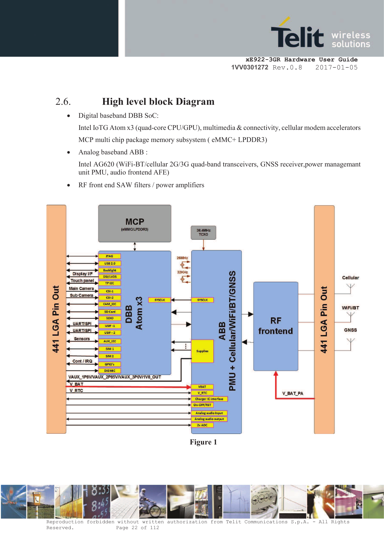


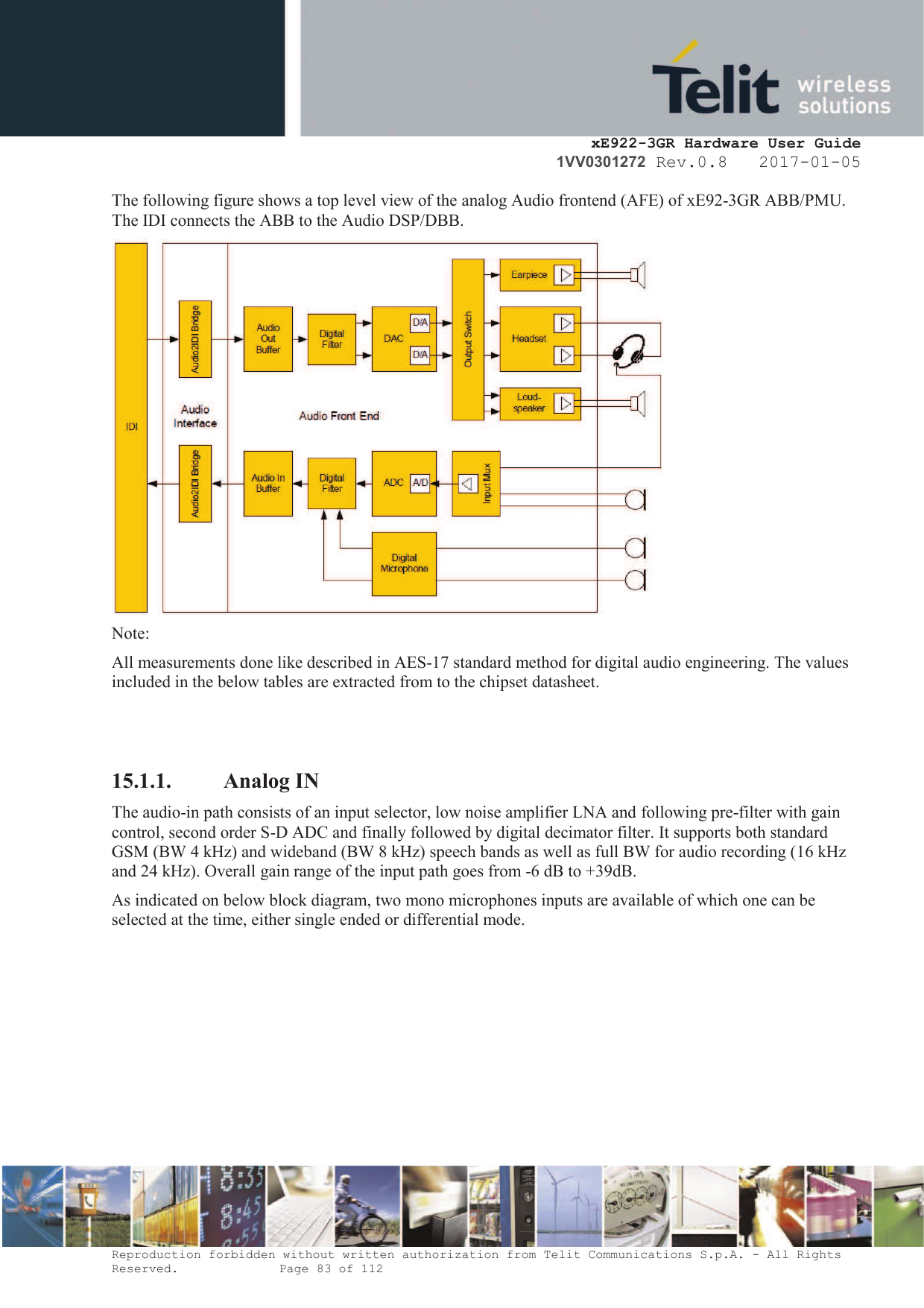
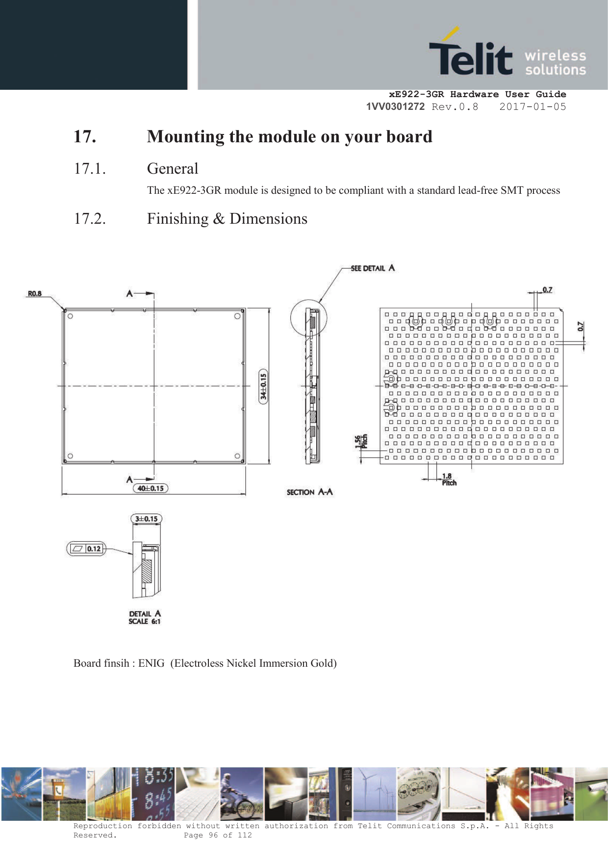
![xE922-3GR Hardware User Guide 1VV0301272 Rev.0.8 2017-01-05 Reproduction forbidden without written authorization from Telit Communications S.p.A. - All Rights Reserved. Page 39 of 112 4. Electrical specifications 4.1. Absolute maximum ratings – not operational A deviation from listed below values range may harm the xE922-3GR module. Symbol Parameter Min Max Unit VBATT battery supply voltage on pin VBATT -0.3 +5.5 [V] VBATT_PA battery supply voltage on pin VBATT_PA -0.3 +6.0 [V] 4.2. Recommended operating conditions Symbol Parameter Min Typ Max Unit Tcase Case temperature (1) -40 +25 +85 [°C] VBATT Battery supply voltage on pin VBATT 3.6 3.8 4.2 [V] VBATT_PA Battery supply voltage on pin VBATT_PA 3.6 3.8 4.2 [V] IBATT_PA + IBATT Peak current to be used to dimension decoupling capacitors on pin VBATT_PA - 2 - [A] (1) Tcase case temperature: measured at top side shield of module 4.3. Logic Level Specifications Unless otherwise specified, all the interface circuits of the xE922-3GR are 1.8V CMOS logic. Only few specific interfaces (such as USIM) are capable of dual voltage I/O. The following table shows the logic level specifications used in the Telit xE922-3GR interface circuits: NOTE: Do not connect xE922-3GR’s digital logic signal directly to OEM’s digital logic signal with a level higher than 2.1V for 1.8V CMOS signals.](https://usermanual.wiki/Telit-Communications-S-p-A/WE9223GR/User-Guide-3349821-Page-39.png)
![xE922-3GR Hardware User Guide 1VV0301272 Rev.0.8 2017-01-05 Reproduction forbidden without written authorization from Telit Communications S.p.A. - All Rights Reserved. Page 40 of 112 For 1.8V CMOS signals: Absolute Maximum Ratings - Not Functional Parameter xE922-3GR Min Max Input level on any digital pin when on -0.3V +2.16V Input voltage on analog pins when on -0.3V +2.16 V Operating Range - Interface levels (1.8V CMOS) Parameter xE922-3GR Unit condition Min Max VIH Input high level 1.3V 2.1V [V] VIL Input low level -0.3V 0.5V [V] VOH Output high level 1.6V [V] Ioh= 0.1 mA VOL Output low level 0.2V [V] Ioh = -0.1mA IIL Low-level input current 1.5 [µA] no PU/PD IIH High-level input current 1.3 [µA] no PU/PD RPU/PD pull up/down resistance 7.2 45 [kΩ] I_source/sink GPIO drive strength 2 12 [mA] Configurable 2,4,8,12 mA Vdrv_HIGH=1.62V/LOW=0.18V](https://usermanual.wiki/Telit-Communications-S-p-A/WE9223GR/User-Guide-3349821-Page-40.png)
![xE922-3GR Hardware User Guide 1VV0301272 Rev.0.8 2017-01-05 Reproduction forbidden without written authorization from Telit Communications S.p.A. - All Rights Reserved. Page 45 of 112 Current max Pull-downr resistor Rpd 200 ohm DC/DC is OFF Switching frequency F_dcdc -3% 3.2 +3% MHz Note: 1V8_OUT is also applied internally the module feeding several I/O peripherals, memory interface and analog RF parts (depending on use case). Care should be exercised to keep external current dissipation limited in order not to exceed the maximum output current of the DC/DC regulator. 1V8_OUT external usage is primarily targeted for IO reference level or supplying levelshift devices. 5.3. Typical system power consumption Test conditions: · room temperature 22deg, still air, no heatsink · V_BAT/V_BAT_PA= 3.8V · 50 ohm antenna load impedance · Display and camera supply current excluded (separately powered) WLAN related use cases are executed with WiFi hotspot serving the DUT as only client, inside RF shield box. These are typical power consumption measured at room temperature, with the module mounted on Telit’s reference carrier board, no heatsink applied. At higher ambient temperature condition one can expect higher current consumption due to increasing leakage currents. SW release: MR1 // sf3gr_telit_he922-flashfiles-eng.android_a60_ww33_camera_orientation. Type description [mA] off Module powered off 0.15 idle Idle Display On 200 WLAN Active Idle (3G cell registered) 18 3G Active Idle 21](https://usermanual.wiki/Telit-Communications-S-p-A/WE9223GR/User-Guide-3349821-Page-45.png)

![xE922-3GR Hardware User Guide 1VV0301272 Rev.0.8 2017-01-05 Reproduction forbidden without written authorization from Telit Communications S.p.A. - All Rights Reserved. Page 48 of 112 The following table gives an overview of V_RTC minimum voltage level requirements in order to keep RTC running: condition minimum V_RTC [V] min Typ max room temperature 0.8 1.1 -40 to +125deg 0.9 1.2 So typically at room temperature a voltage difference of 2.3V – 0.8V = 1.5V is available for buffering the RTC supply in case V_BAT is removed. An external capacitor for RTC buffering can be added, typical 100uF, up to maximum 220uF directly to the LGA pin V_RTC. In case an extreme large (super) capacitor, typical 1 F, is applied, a series resistor of typical 470 Ohm should be added. Typical current drawn from V_RTC by the RTC clock: 2.6µA An RTC alarm is one of the possible events to power ON the module.](https://usermanual.wiki/Telit-Communications-S-p-A/WE9223GR/User-Guide-3349821-Page-48.png)

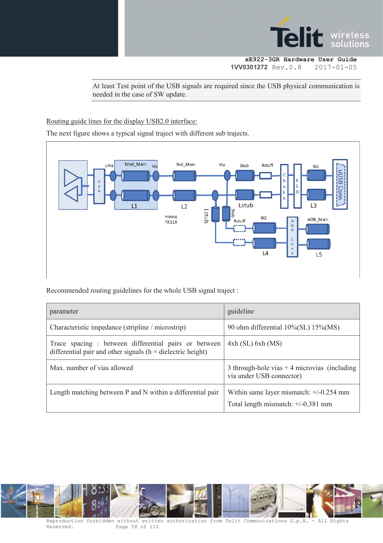
![xE922-3GR Hardware User Guide 1VV0301272 Rev.0.8 2017-01-05 Reproduction forbidden without written authorization from Telit Communications S.p.A. - All Rights Reserved. Page 59 of 112 Guidelines for sub trajects: parameter module main Bi1 Bi2 AOB stub Transmission line segment L1 (MS/SL) L2 (SL) L3 (MS) L4 (MS) L5(SL) Lstub Max. length [mm] 25.4 101.6 12.7 25.4 101.6 5.1 Actual xE922-3GR module signal trace (L1) implementation: signal name module trace length [mm] Number of microvias on the module USB_DP 5.06 3 USB_DN 5.29 3](https://usermanual.wiki/Telit-Communications-S-p-A/WE9223GR/User-Guide-3349821-Page-59.png)
![xE922-3GR Hardware User Guide 1VV0301272 Rev.0.8 2017-01-05 Reproduction forbidden without written authorization from Telit Communications S.p.A. - All Rights Reserved. Page 61 of 112 Recommended routing guidelines for the whole MIPI-DSI signal traject: parameter guideline Characteristic impedance (stripline / microstrip) 100 ohm differential 10%(SL) 15%(MS) Trace spacing : between differential pairs or between differential pair and other signals (h = dielectric height) 5xh (SL) 7xh (MS) Total length (module (L1+L2) + carrier(L3)+add-on pcb(L4) + FPC cable(L5)) Min. 50.8 mm / Max. 152.4 mm (MS/SL) Max. number of vias allowed 4 through-hole vias + 4 microvias + 2 connector pins Length matching between P and N within a differential pair Within same layer mismatch: +/-0.254 mm Total length mismatch: +/-0.381 mm Length matching between DATA to CLK Within same layer mismatch : +/- 1.27 mm Total length mismatch: +/- 2.54 mm Guidelines for off-module sub trajects: parameter Carrier board Addon board FPC cable Transmission line segment L3 L4 L5 Length [mm] 50.8 - 83.8 (MS/SL) 12.7 - 25.4 (MS) 50.8 - 127](https://usermanual.wiki/Telit-Communications-S-p-A/WE9223GR/User-Guide-3349821-Page-61.png)
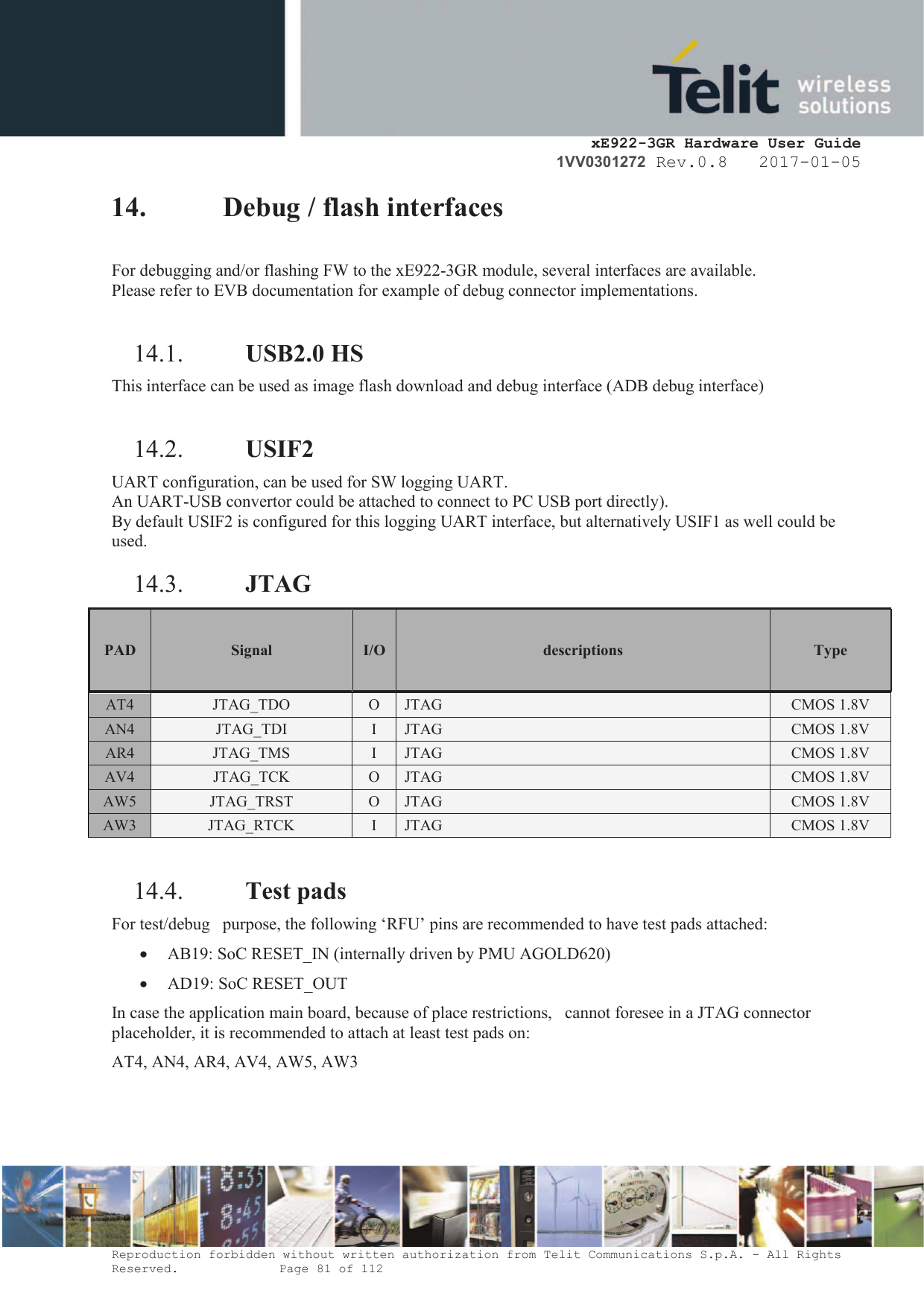
![xE922-3GR Hardware User Guide 1VV0301272 Rev.0.8 2017-01-05 Reproduction forbidden without written authorization from Telit Communications S.p.A. - All Rights Reserved. Page 62 of 112 Actual xE922-3GR module signal trace (L1+L2) implementation: signal name module trace length [mm] Number of microvias on the module DSI_CLKN 9.88 2 DSI_CLKP 9.65 2 DSI_DN0 7.39 2 DSI_DP0 7.15 2 DSI_DN1 9.09 2 DSI_DP1 9.28 2 DSI_DN2 8.60 2 DSI_DP2 8.43 2 DSI_DN3 12.16 2 DSI_DP3 12.01 2 10.2. LVDS 4-lane ‘Low voltage differential signaling’ LVDS transmitter, implementing the LVDS PHY with electrical parameters according TIA/EIA-644 technical standard. LVDS Clock range: 20 – 170 MHz. PAD Signal I/O descriptions Type LVDS Display Interface W19 LVDS_TA1P AO LVDS Data A Positive Analog U19 LVDS_TA1N AO LVDS Data A Negative Analog X18 LVDS_TB1P AO LVDS Data B Positive Analog V18 LVDS_TB1N AO LVDS Data B Negative Analog V20 LVDS_TC1P AO LVDS Data C Positive Analog T20 LVDS_TC1N AO LVDS Data C Negative Analog Y21 LVDS_TD1P AO LVDS Data D Positive Analog W21 LVDS_TD1N AO LVDS Data D Negative Analog U21 LVDS_TCLK1P AO LVDS Clock Positive Analog](https://usermanual.wiki/Telit-Communications-S-p-A/WE9223GR/User-Guide-3349821-Page-62.png)
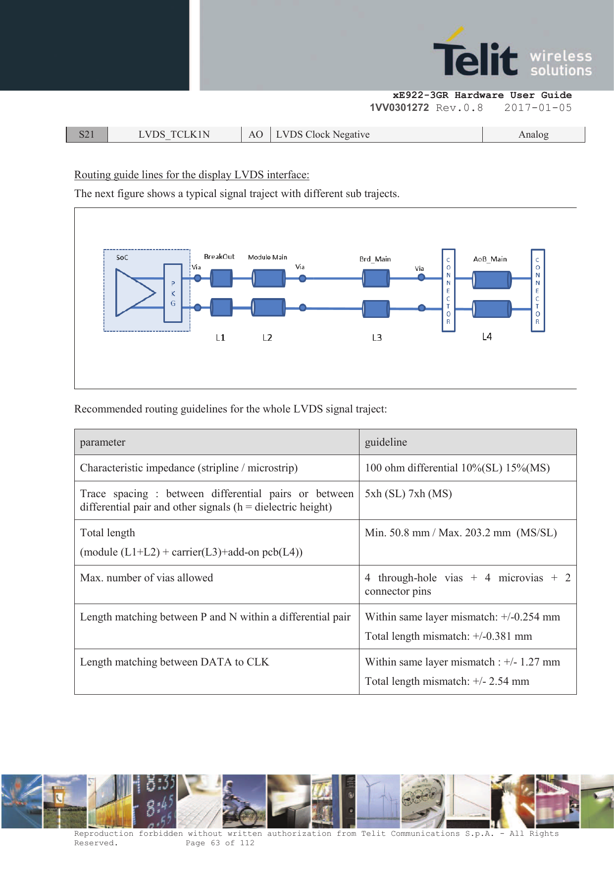
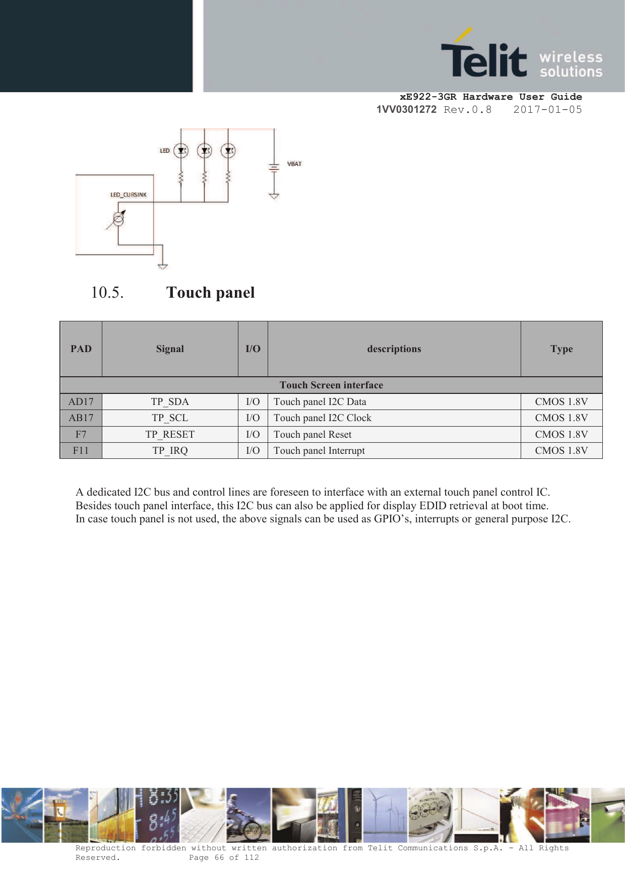
![xE922-3GR Hardware User Guide 1VV0301272 Rev.0.8 2017-01-05 Reproduction forbidden without written authorization from Telit Communications S.p.A. - All Rights Reserved. Page 64 of 112 Guidelines for off-module sub trajects: parameter Carrier board Addon board Transmission line segment L3 L4 Length [mm] 82.5 (MS/SL) Max. 203.2 – (L1+L2+L3) Actual xE922-3GR module signal trace (L1+L2) implementation: signal name module trace length [mm] Number of microvias on the module LVDS_TCLK1N 10.47 2 LVDS_TCLK1P 10.46 2 LVDS_TA1N 9.12 2 LVDS_TA1P 9.31 2 LVDS_TB1N 8.25 2 LVDS_TB1P 8.51 2 LVDS_TC1N 8.16 2 LVDS_TC1P 7.99 2 LVDS_TD1N 12.64 2 LVDS_TD1P 12.46 2 10.3. Backlight control PAD Signal I/O descriptions Type LCD Backlight AS15 CABC AI Content Adaptive Backlight Control Analog AS17 LEDFB_DP AI Backlight feedback Positive Analog AU17 LEDFB_DN AI Backlight feedback Negative Analog AP13 LEDDRV AO Backlight Drive Analog The LED current generator feature can generate supply current for display or keypad backlight LED’s](https://usermanual.wiki/Telit-Communications-S-p-A/WE9223GR/User-Guide-3349821-Page-64.png)
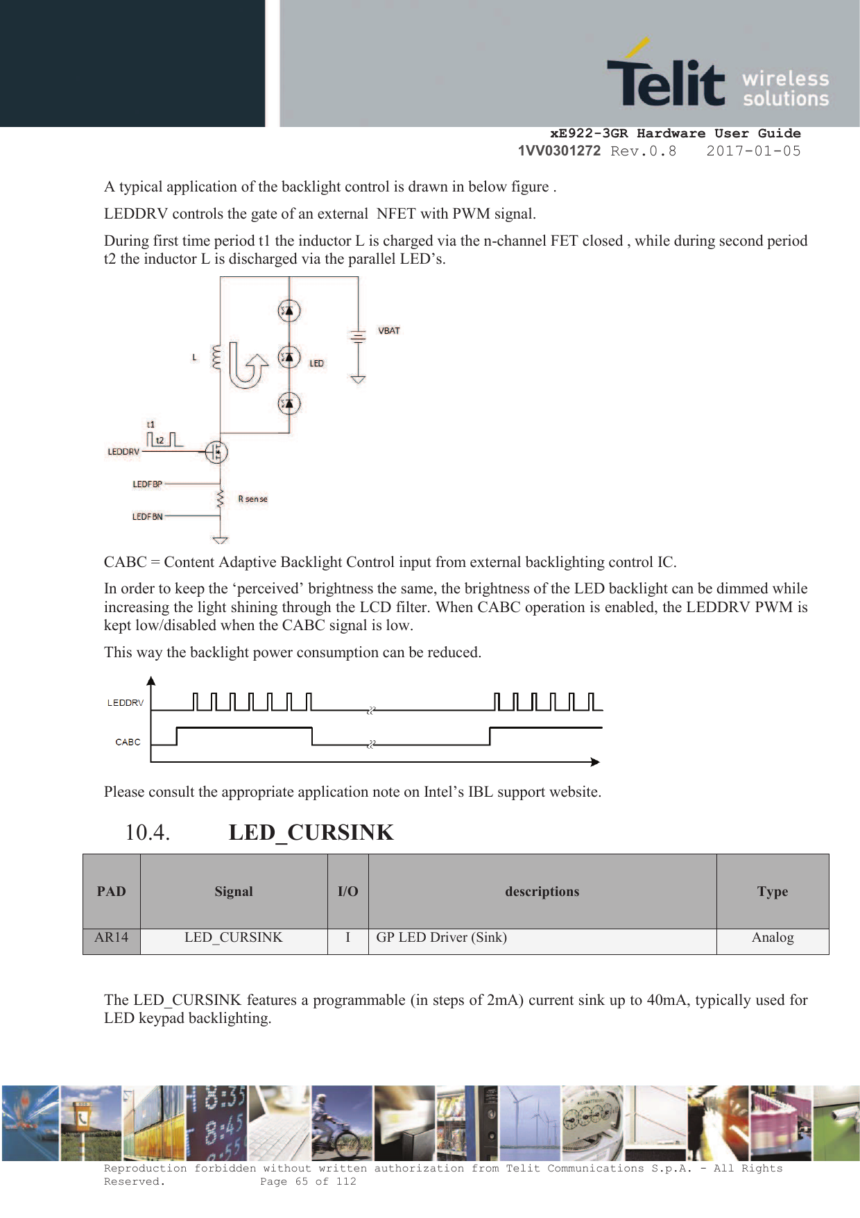
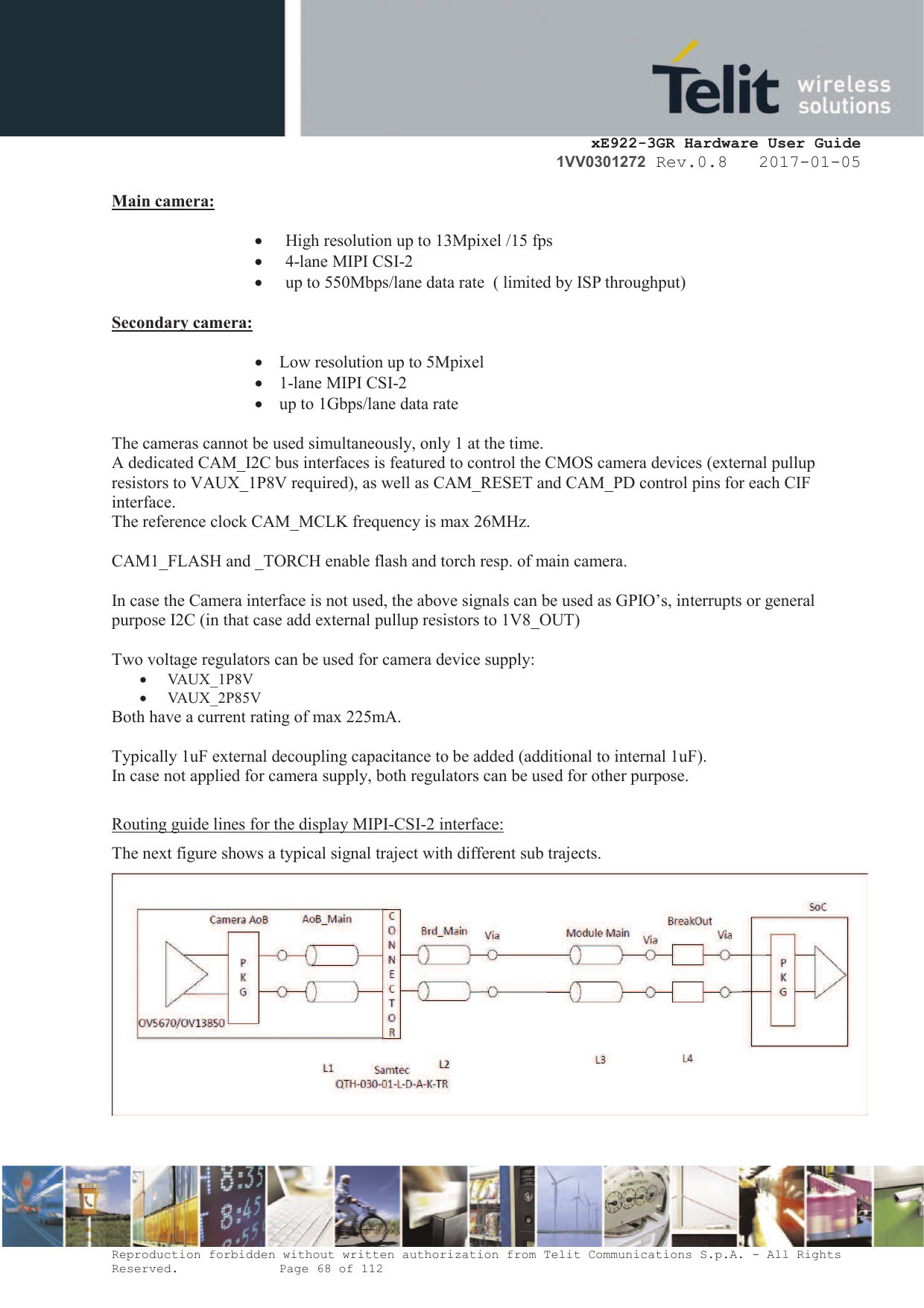
![xE922-3GR Hardware User Guide 1VV0301272 Rev.0.8 2017-01-05 Reproduction forbidden without written authorization from Telit Communications S.p.A. - All Rights Reserved. Page 69 of 112 Recommended routing guidelines for the whole MIPI-CSI-2 signal traject : parameter guideline Characteristic impedance (stripline / microstrip) 100 ohm differential 10%(SL) 15%(MS) Trace spacing : between differential pairs or between differential pair and other signals (h = dielectric height) 5xh (SL) 7xh (MS) Total length (add-on pcb (L1)+ carrier (L2)+ (module (L3+L4)) Min. 45.7 mm / Max. 203.2 mm (MS/SL) Max. number of vias allowed 2 through-hole vias + 3 microvias + 2 connector pins Length matching between P and N within a differential pair Within same layer mismatch: +/-0.254 mm Total length mismatch: +/-0.381 mm Length matching between DATA to CLK Within same layer mismatch : +/- 1.27 mm Total length mismatch: +/- 2.54 mm Guidelines for off-module sub trajects: parameter Addon board Carrier board Transmission line segment L1 L2 Length [mm] 12.7 – 63.5 (MS) 12.7 – 88.9 (MS/SL) Actual xE922-3GR module signal trace (L3+L4) implementation: signal name module trace length [mm] Number of microvias on the module CSI1_CLKN 9.99 2 CSI1_CLKP 9.79 2 CSI1_DN0 10.97 2 CSI1_DP0 11.22 2 CSI1_DN1 7.26 2](https://usermanual.wiki/Telit-Communications-S-p-A/WE9223GR/User-Guide-3349821-Page-69.png)
![xE922-3GR Hardware User Guide 1VV0301272 Rev.0.8 2017-01-05 Reproduction forbidden without written authorization from Telit Communications S.p.A. - All Rights Reserved. Page 70 of 112 CSI1_DP1 7.48 2 CSI1_DN2 7.77 2 CSI1_DP2 7.52 2 CSI1_DN3 7.31 2 CSI1_DP3 7.26 2 signal name module trace length [mm] Number of microvias on the module CSI2_CLKN 10.04 2 CSI2_CLKP 10.26 2 CSI2_DN 10.46 2 CSI2_DP 10.7 2](https://usermanual.wiki/Telit-Communications-S-p-A/WE9223GR/User-Guide-3349821-Page-70.png)
![xE922-3GR Hardware User Guide 1VV0301272 Rev.0.8 2017-01-05 Reproduction forbidden without written authorization from Telit Communications S.p.A. - All Rights Reserved. Page 73 of 112 Actual xE922-3GR module signal trace (L1) implementation USIF1: signal name module trace length [mm] Number of microvias on the module USIF1_SCLK 24.8 3 USIF1_RXD 20.8 3 USIF1_TXD 20.2 3 USIF1_CS 22.2 3 Actual xE922-3GR module signal trace (L1) implementation USIF2: signal name module trace length [mm] Number of microvias on the module USIF2_SCLK 60.8 3 USIF2_RXD 59.2 3 USIF2_TXD 59.4 3 USIF2_CS 58.7 3](https://usermanual.wiki/Telit-Communications-S-p-A/WE9223GR/User-Guide-3349821-Page-73.png)
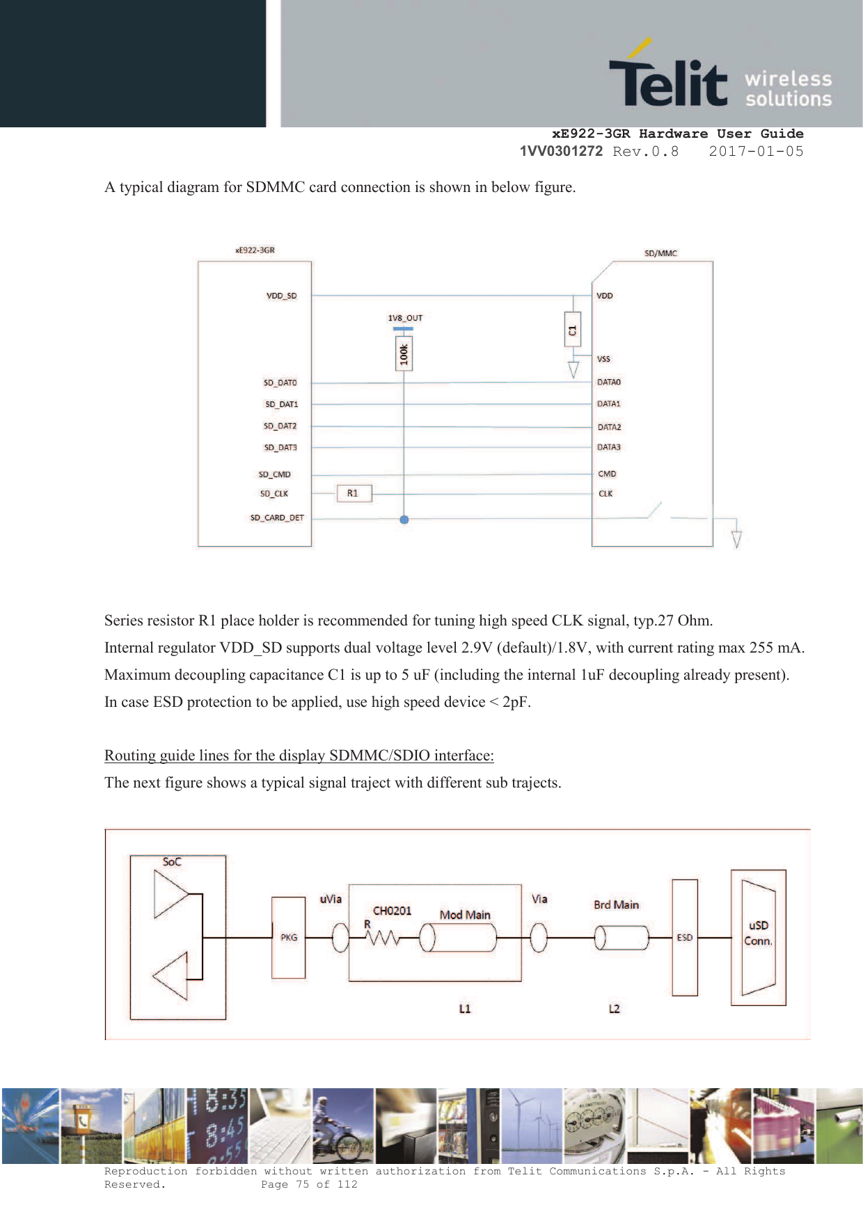
![xE922-3GR Hardware User Guide 1VV0301272 Rev.0.8 2017-01-05 Reproduction forbidden without written authorization from Telit Communications S.p.A. - All Rights Reserved. Page 76 of 112 Recommended routing guidelines for the whole SDMMC/SDIO signal traject: parameter guideline Characteristic impedance (stripline / microstrip) 50 ohm single ended 10%(SL) 15%(MS) Trace spacing (h = dielectric height) 2xh (SL) 3xh (MS) Total length (module (L1) + carrier(L2)) Min. 12.7 mm / Max. 88.9 mm (MS/SL) Max. number of vias allowed 4 through-hole vias + 3 microvias Length matching between DATA/CMD to CLK Within same layer mismatch : +/- 1.27 mm Total length mismatch: +/- 2.54 mm Termination resistors (Note: no series resistors implemented on xE922-3GR module side ) Rseries on CLK is 27 ohm +/-10%, and on DAT 39 ohm +/-10%. The series resistor placeholder should be close to module CLK, DATA and CMD lanes. Use of the resistor is to improve signal quality .Based on validation data, resistor can be removed or retained on the board Actual xE922-3GR module signal trace (L1) implementation: signal name module trace length [mm] Number of microvias on the module SDIO_CLK 18.81 3 SDIO_CMD 18.40 5 SDIO_DAT0 19.85 3 SDIO_DAT1 18.39 4 SDIO_DAT2 17.65 4 SDIO_DAT3 17.62 4](https://usermanual.wiki/Telit-Communications-S-p-A/WE9223GR/User-Guide-3349821-Page-76.png)
![xE922-3GR Hardware User Guide 1VV0301272 Rev.0.8 2017-01-05 Reproduction forbidden without written authorization from Telit Communications S.p.A. - All Rights Reserved. Page 77 of 112 signal name module trace length [mm] Number of microvias on the module SD_CLK 37.86 4 SD_CMD 37.26 4 SD_DAT0 37.79 4 SD_DAT1 36.54 4 SD_DAT2 35.72 4 SD_DAT3 36.49 4 12.4. ADC xE922-3GR offers in total three ADC input lines: PAD Signal I/O descriptions Type AM19 ADC_VBATMEAS I Battery measurement ADC Analog AL18 ADC_IN0 AI Analog to Digital converter 1 (Batt ID) Analog AK19 ADC_IN1 AI Analog to Digital converter 2 (Batt Temp) Analog When the system implements an external battery charger IC circuitry, the above pin description explains the reserved usage in that case. When no charger IC is implemented, ADC_IN0 and _IN1 can be used for general purpose ADC input. ADC_VBATMEAS still needs to be applied at the main supply pin V_BAT of the module in order to properly boot the system. ADC_INx properties: · resolution : 12 bit · input voltage range : 0V … 1.2V (for ADC_IN0/1) · input resistance: minimum 1 MOhm](https://usermanual.wiki/Telit-Communications-S-p-A/WE9223GR/User-Guide-3349821-Page-77.png)
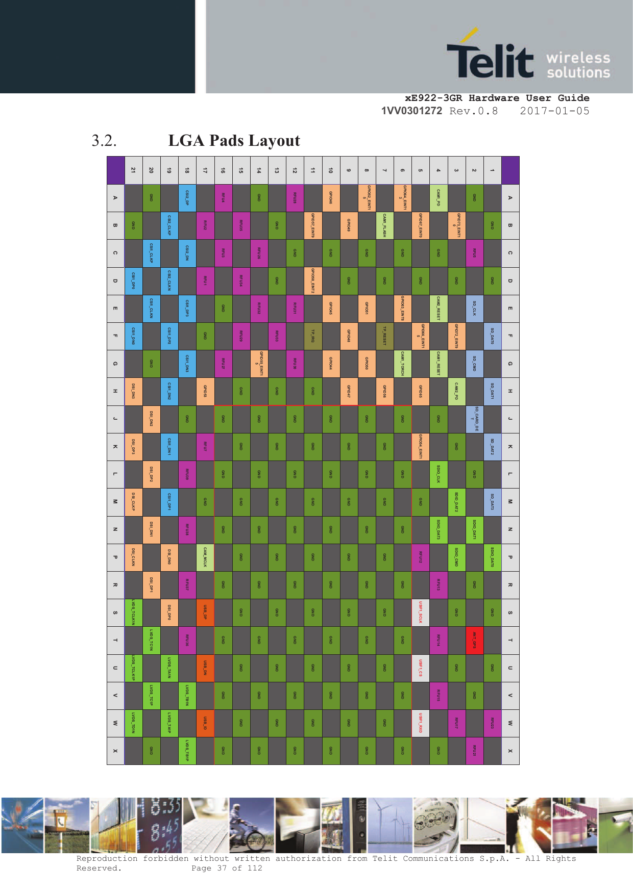
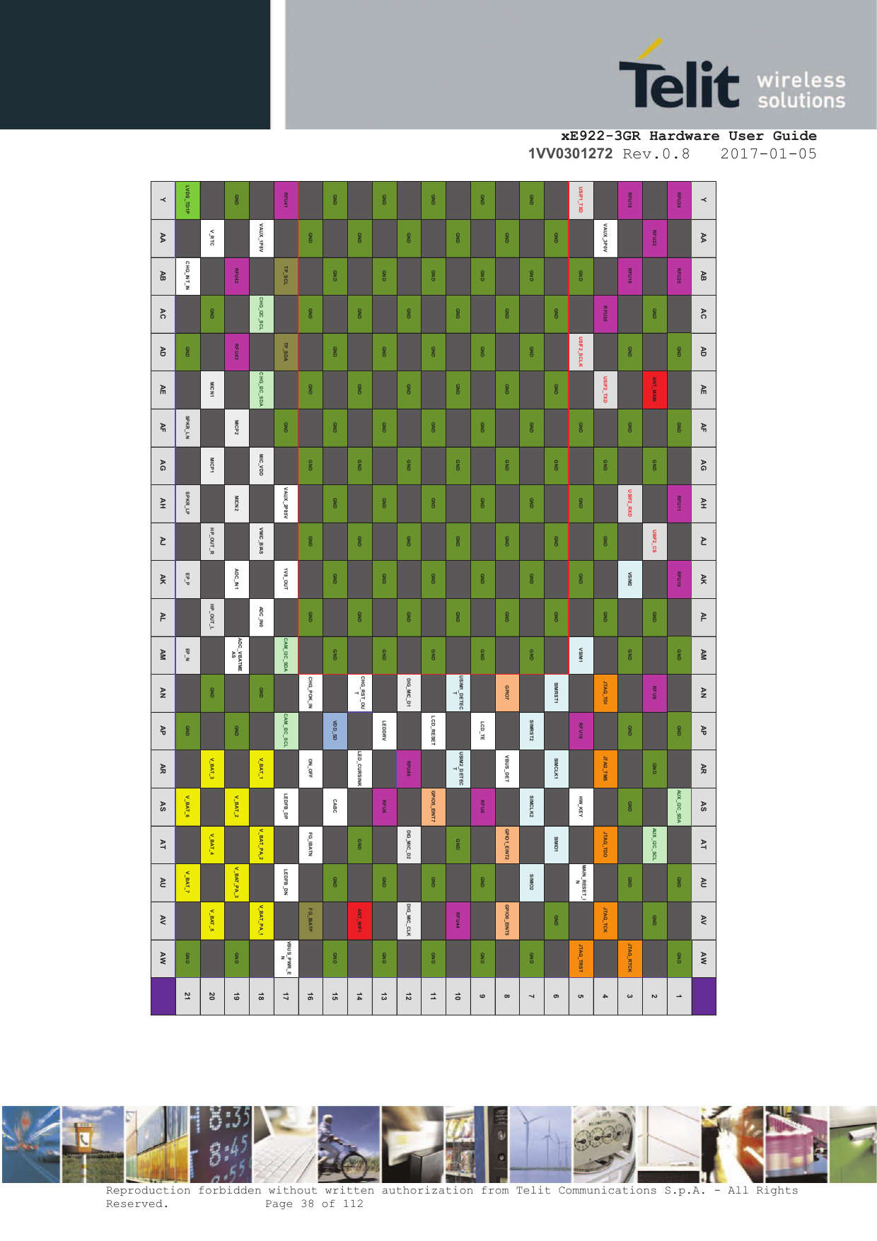
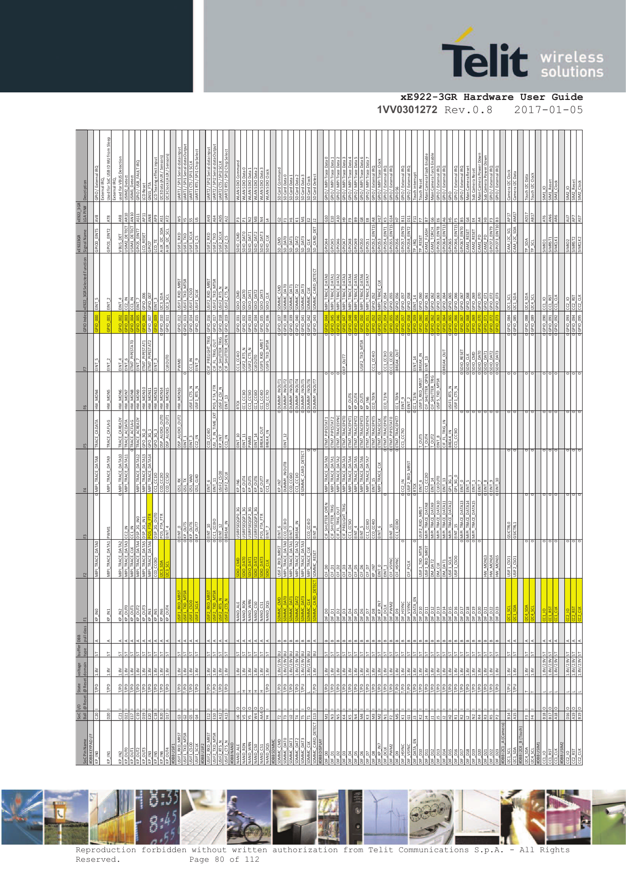
![xE922-3GR Hardware User Guide 1VV0301272 Rev.0.8 2017-01-05 Reproduction forbidden without written authorization from Telit Communications S.p.A. - All Rights Reserved. Page 79 of 112 Each SoC pad’s characteristics are controlled by a peripheral called PCL (Port Control Logic). In the next page table a ‘complete’ overview of all PCL muxing options for ‘all DBB pins externally available’ on the xE922-3GR module LGA pinout is detailed out. In order to clarify the correspondence between the module’s pin naming and chip set supplier documentation naming convention, the DBB SoC BGA ball pin /signal names as well as xE922-3GR LGA pin number / signal names are indicated in different columns. Yellow color code highlights the xE922-3GR module’s intentional target use. Note: Please note GPIO2_EINT4 is applicable as “input only” because of internal level shift circuitry to accommodate for 5V VBUS_USB level detect. Please consult Intel Business Link Support (IBL) for detailed info (like SW user guide) how to program the GPIO configuration/multiplex for your specific application. Each pad has following characteristics indicated: Pad pull class: This is the pull-up and pull-down strength of the pad that can be enabled/disabled using PCL registers. There are three pull classes of pads on 1.8V IO domain, A, B, and D (C is not used). A is the strongest (PU=155uA typ, PD=135uA Typ), B is medium (PU=80.8uA typ, PD=64uA typ) and D is the weakest (PU=16.4uA typ, PD=16.2uA typ). Pull-up/pull-down can be enabled through PCL registers but their strength is fixed as indicated in the GPIO spreadsheet, refer to it for each individual pad’s pull class. Drive strength, also referred to as drive/output current for the pad. 2mA, 4mA, 8mA and 12mA are supported and can be selected by PCL register. Buffer Type: Schmitt Trigger ST or buffer BU. This setting is not selectable through PCL registers. Refer to GPIO spreadsheet for each individual pad’s buffer type. RESET state during RESET (PU or PD): All pads come up in a default state during and after reset until PCL registers are initialized. It is important to note that connection of each GPIO to application circuit requires determination whether application circuit is sensitive to the GPIO being HIGH or LOW at reset, e.g., it might not be desirable to have an RF transmitter enabled by default during power-on reset so the GPIO allocated to its RESET and/or power-down input should be such that it holds the transmitter in “disabled” state at the time of power-on until SW takes control. Refer to GPIO table for each individual pad’s default state at reset. Signal direction during RESET (input or output): Refer to GPIO table for each individual pad’s default direction at reset. Functions multiplexed on each pad: Each pad not associated with dedicated interfaces can have up to 7 alternate functions multiplexed on it in addition to GPIO function. Refer to GPIO table for each individual pad’s alternate functions. Interrupts: the chip set supports sixteen external interrupts (EINT[15:0]) signals that are multiplexed on different pins but can only be used in one location. Not all interrupt signals are available as some are on pins used for dedicated functions. GPIOs and their different aspects described above can be configured through SW. Please refer to software architecture document for more details.](https://usermanual.wiki/Telit-Communications-S-p-A/WE9223GR/User-Guide-3349821-Page-79.png)
![xE922-3GR Hardware User Guide 1VV0301272 Rev.0.8 2017-01-05 Reproduction forbidden without written authorization from Telit Communications S.p.A. - All Rights Reserved. Page 97 of 112 17.3. Recommended foot print for the application main board 441 pads transparant top view Dimensions are in [mm].In order to easily rework the xE922-3GR it is suggested to consider that the application has a 1.5 mm placement inhibit area around the module. It is also suggested, as a common rule for an SMT component, to avoid having a mechanical part of the application in direct contact with the module.](https://usermanual.wiki/Telit-Communications-S-p-A/WE9223GR/User-Guide-3349821-Page-97.png)