Telit Communications S p A WE9223GR Bluetooth and WiFi module User Manual v1 low quality
Telit Communications S.p.A. Bluetooth and WiFi module v1 low quality
User guide

xE922-3GR
Hardware User Guide
1VV0301272
Rev.0.8 - 2017-01-05

xE922-3GR Hardware User Guide
1VV0301272 Rev.0.8 2017-01-05
Reproduction forbidden without written authorization from Telit Communications S.p.A. - All Rights
Reserved. Page 2 of 112
APPLICABILITY TABLE
APPLICABILITY TABLE 1
PRODUCT
HE922-3GR
WE922-3GR

xE922-3GR Hardware User Guide
1VV0301272 Rev.0.8 2017-01-05
Reproduction forbidden without written authorization from Telit Communications S.p.A. - All Rights
Reserved. Page 3 of 112
SPECIFICATIONS SUBJECT TO CHANGE WITHOUT NOTICE
Notice
While reasonable efforts have been made to assure the accuracy of this document, Telit assumes
no liability resulting from any inaccuracies or omissions in this document, or from use of the
information obtained herein. The information in this document has been carefully checked and
is believed to be entirely reliable. However, no responsibility is assumed for inaccuracies or
omissions. Telit reserves the right to make changes to any products described herein and
reserves the right to revise this document and to make changes from time to time in content
hereof with no obligation to notify any person of revisions or changes. Telit does not assume
any liability arising out of the application or use of any product, software, or circuit described
herein; neither does it convey license under its patent rights or the rights of others.
It is possible that this publication may contain references to, or information about Telit products
(machines and programs), programming, or services that are not announced in your country.
Such references or information must not be construed to mean that Telit intends to announce
such Telit products, programming, or services in your country.
Copyrights
This instruction manual and the Telit products described in this instruction manual may be,
include or describe copyrighted Telit material, such as computer programs stored in
semiconductor memories or other media. Laws in the Italy and other countries preserve for Telit
and its licensors certain exclusive rights for copyrighted material, including the exclusive right
to copy, reproduce in any form, distribute and make derivative works of the copyrighted
material. Accordingly, any copyrighted material of Telit and its licensors contained herein or
in the Telit products described in this instruction manual may not be copied, reproduced,
distributed, merged or modified in any manner without the express written permission of Telit.
Furthermore, the purchase of Telit products shall not be deemed to grant either directly or by
implication, estoppel, or otherwise, any license under the copyrights, patents or patent
applications of Telit, as arises by operation of law in the sale of a product.
Computer Software Copyrights
The Telit and 3rd Party supplied Software (SW) products described in this instruction manual
may include copyrighted Telit and other 3rd Party supplied computer programs stored in
semiconductor memories or other media. Laws in the Italy and other countries preserve for Telit
and other 3rd Party supplied SW certain exclusive rights for copyrighted computer programs,
including the exclusive right to copy or reproduce in any form the copyrighted computer
program. Accordingly, any copyrighted Telit or other 3rd Party supplied SW computer
programs contained in the Telit products described in this instruction manual may not be copied
(reverse engineered) or reproduced in any manner without the express written permission of
Telit or the 3rd Party SW supplier. Furthermore, the purchase of Telit products shall not be
deemed to grant either directly or by implication, estoppel, or otherwise, any license under the
copyrights, patents or patent applications of Telit or other 3rd Party supplied SW, except for
the normal non-exclusive, royalty free license to use that arises by operation of law in the sale
of a product.

xE922-3GR Hardware User Guide
1VV0301272 Rev.0.8 2017-01-05
Reproduction forbidden without written authorization from Telit Communications S.p.A. - All Rights
Reserved. Page 4 of 112
Usage and Disclosure Restrictions
License Agreements
The software described in this document is the property of Telit and its licensors. It is furnished
by express license agreement only and may be used only in accordance with the terms of such
an agreement.
Copyrighted Materials
Software and documentation are copyrighted materials. Making unauthorized copies is
prohibited by law. No part of the software or documentation may be reproduced, transmitted,
transcribed, stored in a retrieval system, or translated into any language or computer language,
in any form or by any means, without prior written permission of Telit
High Risk Materials
Components, units, or third-party products used in the product described herein are NOT fault-
tolerant and are NOT designed, manufactured, or intended for use as on-line control equipment
in the following hazardous environments requiring fail-safe controls: the operation of Nuclear
Facilities, Aircraft Navigation or Aircraft Communication Systems, Air Traffic Control, Life
Support, or Weapons Systems (“High Risk Activities"). Telit and its supplier(s) specifically
disclaim any expressed or implied warranty of fitness for such High Risk Activities.
Trademarks
TELIT and the Stylized T Logo are registered in Trademark Office. All other product or service
names are the property of their respective owners.
Copyright © Telit Communications S.p.A. 2016.

xE922-3GR Hardware User Guide
1VV0301272 Rev.0.8 2017-01-05
Reproduction forbidden without written authorization from Telit Communications S.p.A. - All Rights
Reserved. Page 5 of 112
Contents
1. Introduction ..................................................... 9
1.1. Scope ....................................................... 9
1.2. Audience ..................................................... 9
1.3. Contact Information, Support ....................................... 10
1.4. Text Conventions............................................... 10
1.5. Supporting documents ........................................... 11
1.6. Product Variants ............................................... 11
1.7. Abbreviations ................................................. 11
2. General Product Description ......................................... 13
2.1. Overview .................................................... 13
2.2. General Functionality and Main Features ............................... 15
2.3. Reference table of RF bands characteristics ............................. 19
2.3.1. Cellular network: ................................................. 19
2.3.2. WiFi/Bluetooth .................................................. 20
2.3.3. GNSS ........................................................ 20
2.4. Applications .................................................. 20
2.5. Sensitivity ................................................... 21
2.6. High level block Diagram ......................................... 22
2.7. Environmental requirements ....................................... 23
2.7.1. Temperature range ................................................ 23
2.8. xE922-3GR Mechanical Specifications ................................ 24
2.8.1. Dimensions ..................................................... 24
2.8.2. Weight ........................................................ 24
2.8.3. RoHS compliance ................................................ 24
3. xE922-3GR Module pin out .......................................... 25
3.1. PIN table .................................................... 25
3.2. LGA Pads Layout .............................................. 37
4. Electrical specifications ............................................. 39
4.1. Absolute maximum ratings – not operational ............................. 39

xE922-3GR Hardware User Guide
1VV0301272 Rev.0.8 2017-01-05
Reproduction forbidden without written authorization from Telit Communications S.p.A. - All Rights
Reserved. Page 6 of 112
4.2. Recommended operating conditions .................................. 39
4.3. Logic Level Specifications ........................................ 39
5. Power supply .................................................... 41
5.1. Input supply .................................................. 41
5.2. Output supply ................................................. 42
5.2.1. Linear voltage regulators .................................. 42
5.2.1.1. VAUX_1P8V ............................................... 42
5.2.1.2. VAUX_2P85V .............................................. 43
5.2.1.3. VAUX_3P0V ............................................... 43
5.2.1.4. VSIM1/2 ................................................. 44
5.2.2. DC/DC stepdown ................................................. 44
5.2.2.1. 1V8_OUT ................................................. 44
5.3. Typical system power consumption ................................... 45
5.4. RTC backup .................................................. 47
6. Power ON/OFF and reset control ...................................... 49
6.1. Power On .................................................... 49
6.1.1. ON_OFF key action ............................................... 49
6.1.2. Switching ON due to charging ........................................ 50
6.1.3. Switching on due to RTC alarm ....................................... 50
6.2. Power off .................................................... 50
6.2.1. Soft power off ................................................... 50
6.2.2. Emergency power off .............................................. 50
6.3. Reset ....................................................... 50
7. Battery management .............................................. 51
7.1. Coulomb counter ............................................... 51
7.2. Battery charging ............................................... 52
7.2.1. Block diagram ................................................... 52
7.2.2. Battery/charger-less operation ........................................ 54
8. USIM interface .................................................. 55
9. USB port ....................................................... 57
10. Display interface ................................................ 60
10.1. MIPI-DSI .................................................. 60

xE922-3GR Hardware User Guide
1VV0301272 Rev.0.8 2017-01-05
Reproduction forbidden without written authorization from Telit Communications S.p.A. - All Rights
Reserved. Page 7 of 112
10.2. LVDS ..................................................... 62
10.3. Backlight control ............................................. 64
10.4. LED_CURSINK ............................................. 65
10.5. Touch panel ................................................. 66
11. Camera interface ............................................... 67
12. Peripheral interfaces ............................................. 71
12.1. I2C ...................................................... 71
12.2. USIF ..................................................... 72
12.3. SDMMC/SDIO .............................................. 74
12.4. ADC ..................................................... 77
13. General purpose I/O ............................................. 78
14. Debug / flash interfaces ........................................... 81
14.1. USB2.0 HS ................................................. 81
14.2. USIF2 .................................................... 81
14.3. JTAG ..................................................... 81
14.4. Test pads ................................................... 81
15. Audio ........................................................ 82
15.1. Analog .................................................... 82
15.1.1. Analog IN...................................................... 83
15.1.2. Analog OUT .................................................... 86
15.1.2.1. Earpiece ................................................. 87
15.1.2.2. Headset .................................................. 87
15.1.2.3. Loudspeaker .............................................. 88
15.2. Digital .................................................... 90
15.2.1. I2S .......................................................... 90
15.2.2. Digital microphone ................................................ 90
16. Antenna(s) .................................................... 91
16.1. GSM/WCDMA Antenna Requirements ............................. 91
16.1.1. GSM/WCDMA Antenna – PCB line Guidelines............................. 92
16.1.2. GSM/WCDMA Antenna – Installation Guidelines ........................... 92

xE922-3GR Hardware User Guide
1VV0301272 Rev.0.8 2017-01-05
Reproduction forbidden without written authorization from Telit Communications S.p.A. - All Rights
Reserved. Page 8 of 112
16.2. WiFi/BT Antenna Requirements ................................... 93
16.3. GNSS Antenna Requirements .................................... 93
16.3.1. Combined GNSS Antenna .......................................... 94
16.3.2. Linear and Patch GNSS Antenna ..................................... 94
16.3.3. Front End Design Considerations ..................................... 94
16.3.4. GNSS Antenna - PCB Line Guidelines ................................. 95
16.3.5. GNSS Antenna – Installation Guidelines ................................ 95
17. Mounting the module on your board .................................. 96
17.1. General .................................................... 96
17.2. Finishing & Dimensions ........................................ 96
17.3. Recommended foot print for the application main board .................... 97
17.4. Stencil .................................................... 98
17.5. PCB Pad Design .............................................. 98
17.6. Recommendations for PCB Pad Dimensions (mm) ....................... 99
17.7. Solder Paste ................................................ 100
17.7.1. Solder Reflow .................................................. 100
18. Packing system ................................................ 102
18.1. Tray Drawing .............................................. 104
18.2. Moisture Sensitivity .......................................... 105
19. Safety Recommendations ......................................... 106
20. Conformity assessment issues ...................................... 107
20.1. FCC/IC Regulatory notices ...................................... 107
20.1.1. Modification statement ............................................ 107
20.1.2. Interference statement ............................................. 107
20.1.3. RF exposure ................................................... 107
20.1.4. FCC Class B digital device notice ..................................... 108
20.1.5. Labelling Requirements for the Host device .............................. 108
20.2. 1999/5/EC Directive .......................................... 109
21. Document History .............................................. 112

xE922-3GR Hardware User Guide
1VV0301272 Rev.0.8 2017-01-05
Reproduction forbidden without written authorization from Telit Communications S.p.A. - All Rights
Reserved. Page 9 of 112
1. Introduction
1.1. Scope
The aim of this document is to introduce Telit xE922-3GR modules as well as present possible
and recommended hardware solutions useful for developing a product based on the xE922-3GR
modules. All the features and solutions detailed are applicable to all xE922-3GR, where
“xE922-3GR” refers to the modules listed in the applicability table.
If a specific feature is applicable to a specific product, it will be clearly highlighted.
NOTICE:
The description text “xE922-3GR” refers to all modules listed in the APPLICABILITY TABLE 1.
In this document all the basic functions of a wireless module will be taken into account; for
each one of them a valid hardware solution will be suggested and usually incorrect solutions
and common errors to be avoided will be highlighted. Obviously this document cannot embrace
every hardware solution or every product that may be designed. Obviously avoiding invalid
solutions must be considered as mandatory. Whereas the suggested hardware configurations
need not be considered mandatory, the information given should be used as a guide and a
starting point for properly developing your product with the Telit xE922-3GR module.
NOTICE:
The integration of the GSM/GPRS/EGPRS/WCDMA/HSPA+/WiFi/BT/GNSS xE922-3GR
cellular module within user application must be done according to the design rules described in
this manual.
The information presented in this document is believed to be accurate and reliable. However,
no responsibility is assumed by Telit Communication S.p.A. for its use, such as any
infringement of patents or other rights of third parties which may result from its use. No
license is granted by implication or otherwise under any patent rights of Telit Communication
S.p.A. other than for circuitry embodied in Telit products. This document is subject to change
without notice.
1.2. Audience
This document is intended for Telit customers, especially system integrators, about to
implement their applications using the Telit xE922-3GR module.
xE922-3GR Hardware User Guide
1VV0301272 Rev.0.8 2017-01-05
Reproduction forbidden without written authorization from Telit Communications S.p.A. - All Rights
Reserved. Page 10 of 112
1.3. Contact Information, Support
For general contact, technical support, to report documentation errors and to order manuals,
contact Telit’s Technical Support Center (TTSC) at:
TS-NORTHAMERICA@telit.com if located in North America
For other regions, Collabnet Telit web portal can be used at https://teamforge.telit.com (account
can be asked at support.collabnet@telit.com
Alternatively, use:
http://www.telit.com/en/products/technical-support-center/contact.php
For detailed information about where you can buy the Telit modules or for recommendations
on accessories and components visit:
http://www.telit.com
To register for product news and announcements or for product questions contact Telit’s
Technical Support Center (TTSC).
Our aim is to make this guide as helpful as possible. Keep us informed of your comments and
suggestions for improvements.
Telit appreciates feedback from the users about the information provided.
1.4. Text Conventions
Danger – This information MUST be followed or catastrophic equipment failure or bodily
injury may occur.
Caution or Warning – Alerts the user to important points about integrating the module, if
these points are not followed, the module and end user equipment may fail or malfunction.
Tip or Information – Provides advice and suggestions that may be useful when integrating
the module.
All dates are in ISO 8601 format, i.e. YYYY-MM-DD.
xE922-3GR Hardware User Guide
1VV0301272 Rev.0.8 2017-01-05
Reproduction forbidden without written authorization from Telit Communications S.p.A. - All Rights
Reserved. Page 11 of 112
1.5. Supporting documents
· 1VV0301249_EVB USER GUIDE.pdf
· 1VV0301285_IFBD HW User Guide xE922-3GR.pdf
· 1VV0301324_MMI_EXT_CARD_xE922_3GR_HW USER GUIDE
· 80504NT11473A Thermal Guidelines.pdf
For further detailed information, HW/SW user manuals and application notes related to the INTEL chipset
applied for this RF module, please consult Intel Business Link Support (IBL): https://businessportal.intel.com
1.6. Product Variants
xE922-3GR is available in the following hardware variants:
Type Number
Description
HE922-3GR
GSM/GPRS/EGPRS/WCDMA/HSPA+/WiFi/BT/GNSS
WE922-3GR
WiFi/BT/GNSS
1.7. Abbreviations
Term
Definition
ABB
Analog baseband
ADC
Analog-to-digital converter
AE
Application-Enabled
AES-NI
Advanced Encryption Standard New Instructions
AFE
Audio FrontEnd
CABC
Content Adaptive Backlight Control
CDP (USB)
Charging downstream port
CEU
Configurable Encryption Unit
CSI
Camera serial interface
DAC
Digital-to-analog converter
DBB
Digital baseband
DCP (USB)
Dedicated charging port
DBP
dead battery provision
DSI
Display serial interface
DSDS
Dual Sim Dual Standby
EOC
End of charge
EDID
Extended display identification data
FDD
Frequency division duplex
xE922-3GR Hardware User Guide
1VV0301272 Rev.0.8 2017-01-05
Reproduction forbidden without written authorization from Telit Communications S.p.A. - All Rights
Reserved. Page 12 of 112
GLONASS
Global orbiting navigation satellite system
GNSS
Global navigation satellite system
GPIO
General-purpose input/output
GPRS
General packet radio services
GPS
Global positioning system
GSM
Global system for mobile communications
HMI
Human machine interface
I2C
Inter-integrated circuit
ISP
Image Signal Processor
IDI
Inter die interface
LE
Low Energy
LVDS
Low Voltage Differential Signaling
MIPI
Mobile Industry Processor Interface
MS
Microstrip line
PMU
Power management unit
SD
Secure digital
SDP (USB)
Standard downstream port
SL
Strip line
SIM
Subscriber identity module
SOC
System-On-Chip
SOC
State of charge
SMEP
Supervisor Mode Execution Privilege
SPI
Serial peripheral interface
TE
Tearing effect
UART
Universal asynchronous receiver transmitter
UMTS
Universal mobile telecommunications system
USB
Universal serial bus
USIF
Universal serial interface
VMM
Virtual machine manager
VT-x
Intel Virtual Technology
WCDMA
Wideband code division multiple access

xE922-3GR Hardware User Guide
1VV0301272 Rev.0.8 2017-01-05
Reproduction forbidden without written authorization from Telit Communications S.p.A. - All Rights
Reserved. Page 13 of 112
2. General Product Description
2.1. Overview
Telit’s module family xE922-3GR is based on Intel’s IoTG Atom x3 Quad Core processor dual
chip platform.
DBB : SoC Atom x3
· CPU: Quad Core (Silvermont) 1.16 GHz
L1$ I/D 16KB/16KB ; L2$ 1MB
8-ch main application DMA / 4-ch secure DMA
Android 32bit, Linux Yocto 32bit
· GPU: GFX core modified Mali-450 MP4 600 MHz $128KB
· DSP : 2x TeakLite @277MHz
· Media Encode/Decode Engine: modified VeriSilicon Media Engine (dec G1/enc H1)
Video encoding:
• H.264 BP@level4.0, MP@level4.0, HP@level4.0
• Bit rate supported is from 10Kbps to 20Mbps
• JPEG Baseline
Video decoding:
• MPEG-1 Main Profile up to High Level
• MPEG-2 Main Profile up to High Level
• MPEG-4 Simple Profile up to Level 6, Advanced Profile up to Level 5
• H.264 up to HP Level 5.1, up to 1080p 30fps (yocto) /720p 50fps (android)
• HEVC Main Profile up to Level 4.1 High Tier, up to 1080p 30fps (yocto) /720p
50fps (android)
• VP6/VP8
• JPEG Baseline interleaved
· Security building blocks
ABB: AGOLD 620
· 2G/3G RF transceiver
· WLAN
· Bluetooth

xE922-3GR Hardware User Guide
1VV0301272 Rev.0.8 2017-01-05
Reproduction forbidden without written authorization from Telit Communications S.p.A. - All Rights
Reserved. Page 14 of 112
· GNSS
· Audio
· Analog measurement
· Power management
The module incorporates the following key technologies:
· 2G/3G cellular subsystem
· GNSS subsystem
· WiFi and Bluetooth subsystems
· Display subsystem
· Camera subsystem
· Audio subsystem
· Power management
xE922-3GR is designed for commercial (0C to70C) & industrial (extended temperature -40C to
+85C) markets quality needs.
In its most basic use case, xE922-3GR can be applied as a wireless communication front-end for
M2M products, offering GNSS and mobile communication features to an external host CPU
through its rich interfaces.
The module supports data only communication, voice call is not supported.
xE922-3GR can further support customer software applications and security features. xE922-
3GR provides software application environment with sufficient system resources for creating
rich on board applications. Thanks to a dedicated application processor and embedded security
resources, product developers and manufacturers can create products which guarantee fraud
prevention and tamper evidence without extra effort for additional security precautions.
xE922-3GR can be self-sufficient and serve as a fully integrated IoT solution. In such a case,
customer would simply complement the module with a power supply, speaker amplifier,
microphone, antennae and an HMI (if applicable).
xE922-3GR is offered with different variants per the list in Section 1.6:
· HE922-3GR: Cellular/WiFi/BT/GNSS
· WE922-3GR: WiFi/BT/GNSS

xE922-3GR Hardware User Guide
1VV0301272 Rev.0.8 2017-01-05
Reproduction forbidden without written authorization from Telit Communications S.p.A. - All Rights
Reserved. Page 15 of 112
2.2. General Functionality and Main Features
The xE922-3GR family of IoT modules features 2G/3G modem, GNSS and WiFi/BT
connectivity together with an on-chip powerful application processor and a rich set of
interfaces.
This overview sums all key interfaces offered by the module , consult the documentation on
INTEL’s IBL supporting website for actual implementation state.
A) Modem subsystem for data only communication (HE922-3GR variant only)
· 2G technology 3GPP TS 45.005
o GSM/GPRS/EDGE (multislot class 10)
note : only EDGE RX mode supported
o Quad band support (GSM850/E-GSM900/DCS1800/PCS1900)
· 3G technology 3GPP TS 25.101 rel 7
o WCDMA (HSDPA 21Mbps cat14 / HSUPA 5.76Mbps cat6)
o Quad band support ( band 1 / 2 / 5 / 8)
o Class3 power class
· Two (U)SIM ports – dual voltage 1.8/3V
ISO 7816-3 IC card standard
B) GNSS subsystem
§ GPS/GLONASS receiver
§ Assisted GNSS
§ SBAS: WAAS, EGNOS
C) WiFi/Bluetooth subsystem
· WiFi 802.11 b/g/n 1x1 (1-14, max channel width 20MHz)
· BT 4.0 & BLE
· Single antenna shared for WiFi and BT
· Up to 72.2Mbps OTA throughput, 50Mbps actual throughput
D) Audio subsystem
· Embedded analog codec
o 2x microphone inputs + bias supply
o 1x stereo headset output

xE922-3GR Hardware User Guide
1VV0301272 Rev.0.8 2017-01-05
Reproduction forbidden without written authorization from Telit Communications S.p.A. - All Rights
Reserved. Page 16 of 112
o 1x mono earpiece output
o 1x mono speaker (classD 700mW/3.8V/8 ohm)
· Dual digital microphone
· I2S digital audio IO ( pinning multiplexed with USIF1 port)
E) Display subsystem
Up to 1080p, 24-bit color, 1080p 30fps (yocto) /720p 50fps (android)
· MIPI-DSI (one x4 lanes port, tearing effect timing control)
· LVDS (one x4 lanes port)
· 4 display layer
· Support color space conversion :YUV2RGB and RGB2YUV
· Support replication and dithering
· 2D Graphic Engine
· Backlight control (CABC input, BL feedback input, BL drive output)
· I2C port for touch panel control IC
F) Camera subsystem
Up to 13Mpix, 15 fps ( ISP throughput up to 221 Mpix/sec) (8Mpix, 25fps)
· 4 lanes MIPI-CSI for primary camera (up to 13Mpix/1080p)
· One lane MIPI-CSI for secondary camera (up to 5Mpix/720p)
· 1 camera at a time
· GPIO’s for camera control
· I2C port for camera subsystem control
· Camera auxiliary supply output
G) Power management
· External battery charger IC support
o I2C port dedicated to external charger IC control
o Dedicated GPIO’s
o Fuel gauge input, VBAT/DC sourcing sense ADC input
· Ability to supply the module from DC source without external battery charger
IC implementation
· Rich set of embedded power management functions are in place to permit
minimization of the powerconsumption of the system in all operating modes.

xE922-3GR Hardware User Guide
1VV0301272 Rev.0.8 2017-01-05
Reproduction forbidden without written authorization from Telit Communications S.p.A. - All Rights
Reserved. Page 17 of 112
o Reduction of switching power consumption by clock gating.
o Reduction of leakage power by switching off non active logic.
o Dynamic Frequency Voltage Scaling reducing the supply voltage
depending on the perfomance requirements of the system
· The following system operating modes are defined :
o OFF : complete system switched off ( all context lost)
o WORKING : CPU executing scheduled tasks
o IDLE : CPU in power state HALT , waiting for interrupt
o DEEP SLEEP: CPU in power state DORMANT
H) Application processor
The Intel virtual machine manager (VMM) shares CPU resources of the quad core Atom
between the cellular DBB modem high level protocol implementation, the applied OS and
customer applications. Available BSP’s are 32bit Android and 32bit Linux (Yocto project).
The chipset external memory interface controller EMIC supports
· Low power LPDDR3 upto 2Gbyte
clock frequency up to 533MHz (data speed 1066 Mbps/pin)
· embedded MMC card interface eMMC4.51
clock frequency up to 52MHz ( data speed DDR 102 Mbps/pin)
(dataspeed DDR transfer)
Module embedded memory size implementation :
· FLASH eMMC: 8 Gbyte (x8 pin, data speed up to 833 Mbps)
· RAM LPDDR3: 1 Gbyte ( x32 pin, data speed up to 34112 Mbps)
I) Security capabilities of DBB:
Intergrated Trusted Executon Environment (TEE) based on Secure Virtual Machine and
HW Crypto Unit (CEU)
· Atom Quad Core:
VT-x2 / AES-NI / SMEP ( Supervisor Mode Execution Privilege)
· Extensible Secure Execution Environment:
HW crypto accelerator – CEU / 256K SRAM
· Configurable execution unit (CEU):
o DES/3DES
o AES(128,192,256)

xE922-3GR Hardware User Guide
1VV0301272 Rev.0.8 2017-01-05
Reproduction forbidden without written authorization from Telit Communications S.p.A. - All Rights
Reserved. Page 18 of 112
o Exponentiation accelerator – supports RSA(1024.2048)
o Hashing engines : MD5, HMAC, SHA1/256
o True-RNG
· Secure memory : isolated memory region IMR for secure VM
· Secure boot : root of trust is SEC ROM
· Content protection : Widevine Level 1 DRM ( HW protected Video Path)
J) Rich set of module I/O interfaces, including:
· SDIO: SD 3.0, 1x 4bit, speed up to DDR50
only 1.8V supported
· SDMMC: 1x 4bit, default mode (26MHz)
including power supply (fixed 2.9V) and card detect
· USB2.0 (FS/HS DRD dual role device)
The USB port is typically used for:
o Flashing of firmware and module configuration
o Production testing
o Accessing the Application Processor’s filesystem
o AT command access
o High speed WWAN access to external host
o Diagnostic monitoring and debugging
o Communication between Java application environment and an
external host CPU
o NMEA data to an external host CPU
o Connect to USB peripherals or hubs (note: application note available
from chipset provider on USB hub connectivity)
· Peripheral Ports
These can be applied to support several sensors like : accelerometer , gyroscope,
magnetometer, proximity and ambient light sensors
Please consult Intel’s IBL Support website for AVL (approved vendor list), as well
for recommended implemenation and port assignment
· 3x I2C port full speed:

xE922-3GR Hardware User Guide
1VV0301272 Rev.0.8 2017-01-05
Reproduction forbidden without written authorization from Telit Communications S.p.A. - All Rights
Reserved. Page 19 of 112
o I2C_AUX : auxiliary use
o I2C_CAM / I2C_TP : available when not applied for camera and/or
touchpad control
· USIF1 port: configurable as SPI or UART (up to 48MHz) (multiplexed with I2S)
· USIF2 port: configurable as SPI or UART (up to 26MHz)
· 26 general purpose GPIOs with at least 8 interrupts ( more can be available
depending on final product configuration)
· Analog audio I/F
· Antenna RF ports (GNSS, CELLULAR,WIFI/BT)
K) Form factor (40x34mm), 441 pin LGA
L) Single supply module. The module generates all its internal supply voltages.
M) Built-in RTC / backup supply pin for supercap
N) Two Operating temperature range specified for the xE922-3GR family:
· Commercial: 0 °C to +70 °C
· Industrial extended temperature: -40 °C to +85 °C
O) Cellular transmitter can work simultaneously with the transmitter in the 2.4GHz band. Only
one of the 2.4 GHz modes works at a given moment and it can work simultaneously with any
of the cellular modes.
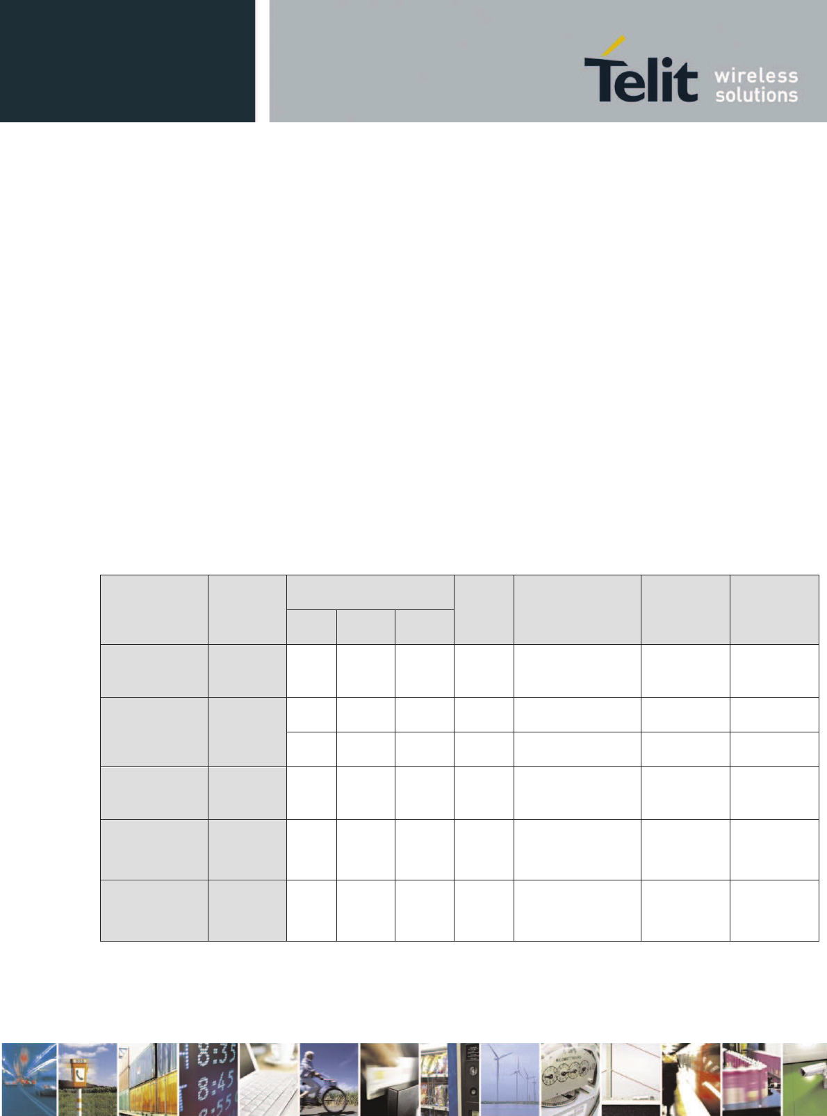
2.3. Reference table of RF bands characteristics
2.3.1. Cellular network:
Mode
Freq. TX
(MHz)
Freq. RX (MHz)
Channels
TX
-
RX offset
PCS 1900
1850.2 ~ 1909.8
1930.2 ~ 1989.8
512 ~ 810
80MHz
DCS 1800
1710 ~ 1785
1805 ~ 1880
512 ~ 885
95MHz
xE922-3GR Hardware User Guide
1VV0301272 Rev.0.8 2017-01-05
Reproduction forbidden without written authorization from Telit Communications S.p.A. - All Rights
Reserved. Page 20 of 112
Mode
Freq. TX
(MHz)
Freq. RX (MHz)
Channels
TX
-
RX offset
GSM 850
824.2 ~ 848.8
869.2 ~ 893.8
128 ~ 251
45MHz
EGSM 900
890 ~ 915
935 ~ 960
0 ~ 124
45 MHz
880 ~ 890
925 ~ 935
975 ~ 1023
45 MHz
WCDMA 2100
–
B1
1920 ~ 1980
2110 ~ 2170
Tx: 9612 ~ 9888
Rx: 10562 ~ 10838
190MHz
WCDMA 1900
–
B2
1850 ~ 1910
1930 ~ 1990
Tx: 9262 ~ 9538
Rx: 9662 ~ 9938
80MHz
WCDMA 850
– B5
824 ~ 849
869
~ 894
Tx: 4132 ~ 4233
Rx: 4357 ~ 4458
45MHz
WCDMA 900
– B8
880 ~ 915
925 ~ 960
Tx: 2712 ~ 2863
Rx: 2937 ~ 3088
45MHz
2.3.2. WiFi/Bluetooth
min typ max unit
Frequency range
2402
-
2482
MHz
2.3.3. GNSS
min
typ
max
unit
GPS
-
1575.5
-
MHz
Glonass
- 1602 - MHz
2.4. Applications
xE922-3GR modules can be used for all kind of IoT Gateways.
Example applications can be:
- Reduction of production overheads
- Smart management of productions
- Remote device monitoring

xE922-3GR Hardware User Guide
1VV0301272 Rev.0.8 2017-01-05
Reproduction forbidden without written authorization from Telit Communications S.p.A. - All Rights
Reserved. Page 21 of 112
- Data retrieval to prevent terror attacks
-
2.5. Sensitivity
· 3G =< -110 dBm
· 2G CS1 =< -111 dBm
· 2G CS4 =< -103 dBm
xE922-3GR Hardware User Guide
1VV0301272 Rev.0.8 2017-01-05
Reproduction forbidden without written authorization from Telit Communications S.p.A. - All Rights
Reserved. Page 22 of 112
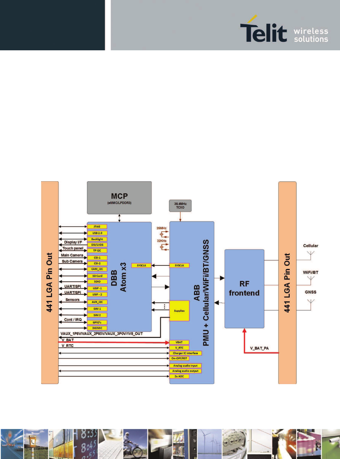
2.6. High level block Diagram
· Digital baseband DBB SoC:
Intel IoTG Atom x3 (quad-core CPU/GPU), multimedia & connectivity, cellular modem accelerators
MCP multi chip package memory subsystem ( eMMC+ LPDDR3)
· Analog baseband ABB :
Intel AG620 (WiFi-BT/cellular 2G/3G quad-band transceivers, GNSS receiver,power managemant
unit PMU, audio frontend AFE)
· RF front end SAW filters / power amplifiers
Figure 1

xE922-3GR Hardware User Guide
1VV0301272 Rev.0.8 2017-01-05
Reproduction forbidden without written authorization from Telit Communications S.p.A. - All Rights
Reserved. Page 23 of 112
2.7. Environmental requirements
2.7.1. Temperature range
Operating
Temperature Range
-20 ~ +55
°C :
This range is defined by 3GPP (the global standard for
wireless mobile communication). Telit guarantees its modules to
comply with all the 3GPP requirements and to have full functionality
of the
module with in this range.
extended temperature
-40 ~ +85°C
& commercial temperature 0~+70°C
:
Telit guarantees full functionality within this range as well. However,
there may possibly be some performance deviations in this extended
range relative to
3GPP requirements,
which means: some RF
parameters may deviate from 3GPP specification in the order of few
dB. For example: receiver sensitivity or maximum output power may
be slightly degraded.
Even so, all the functionalities like
data connection, SMS
, USB
communication, UART activation etc. will be maintained, and the
effect of such degradations will not lead to malfunction.
Storage and non-
operating
Temperature Range
–40°C
~ +105°C

xE922-3GR Hardware User Guide
1VV0301272 Rev.0.8 2017-01-05
Reproduction forbidden without written authorization from Telit Communications S.p.A. - All Rights
Reserved. Page 24 of 112
2.8. xE922-3GR Mechanical Specifications
2.8.1. Dimensions
The Telit xE922-3GR module overall dimensions are:
• Length: 34 mm, +/- 0.15 mm Tolerance
• Width: 40 mm, +/- 0.15 mm Tolerance
• Thickness: 3.0 mm, +/- 0.15 mm Tolerance
2.8.2. Weight
The nominal weight of the xE922-3GR module is 9.7 gram.
2.8.3. RoHS compliance
As a part of Telit corporate policy of environmental protection, the xE922-3GR complies with
the RoHS (Restriction of Hazardous Substances) directive of the European Union (EU directive
2011/65/EU).
xE922-3GR Hardware User Guide
1VV0301272 Rev.0.8 2017-01-05
Reproduction forbidden without written authorization from Telit Communications S.p.A. - All Rights
Reserved. Page 25 of 112
3. xE922-3GR Module pin out
3.1. PIN table
PAD
Signal
I/O
descriptions Type
USB 2.0 Interface
W17
USB_ID
AI
USB_ID, USB DRD use
Analog
S17
USB_DP
I/O
USB differential Data (+)
Analog
U17
USB_DN
I/O
USB differential Data (-)
Analog
AR8
VBUS_DET
I
VBUS detection
Analog
Main Camera
D21
CSI1_DP0
AI
Main Camera CSI Data0 Input Positive
Analog
F21
CSI1_DN0
AI
Main Camera CSI Data0 Input Negative
Analog
M19
CSI1_DP1
AI
Main Camera CSI Data1 Input Positive
Analog
K19
CSI1_DN1
AI
Main Camera CSI Data1 Input Negative
Analog
F19
CSI1_DP2
AI
Main Camera CSI Data2 Input Positive
Analog
H19
CSI1_DN2
AI
Main Camera CSI Data2 Input Negative
Analog
E18
CSI1_DP3
AI
Main Camera CSI Data3 Input Positive
Analog
G18
CSI1_DN3
AI
Main Camera CSI Data3 Input Negative
Analog
C20
CSI1_CLKP
AI
Main Camera CSI Clock Positive
Analog
E20
CSI1_CLKN
AI
Main Camera CSI Clock Negative
Analog
P17
CAM_MCLK
O
Camera MCLK output
CMOS 1.8V
AM17
CAM_I2C_SDA
I/O
Camera I2C Data
CMOS 1.8V
AP17
CAM_I2C_SCL
I/O
Camera I2C Clock
CMOS 1.8V
A4
CAM1_PD
I/O
Main Camera Power Down / GPIO
CMOS 1.8V
G4
CAM1_RESET
I/O
Main Camera Reset / GPIO
CMOS 1.8V
B7
CAM1_FLASH
I/O
Main Camera Flash Triger
CMOS 1.8V
G6
CAM1_TORCH
I/O
Main Camera Torch Enable
CMOS 1.8V
Secondary Camera
A18
CSI2_DP
AI
Sub Camera CSI Data Input Positive
Analog
C18
CSI2_DN
AI
Sub Camera CSI Data Input Negative
Analog
B19
CSI2_CLKP
AI
Sub Camera CSI Clock Positive
Analog
D19
CSI2_CLKN
AI
Sub Camera CSI Clock Negative
Analog
H3
CAM2_PD
I/O
Sub Camera Power Down / GPIO
CMOS 1.8V
E4
CAM2_RESET
I/O
Sub Camera Reset / GPIO
CMOS 1.8V
MIPI DSI Display Interface
xE922-3GR Hardware User Guide
1VV0301272 Rev.0.8 2017-01-05
Reproduction forbidden without written authorization from Telit Communications S.p.A. - All Rights
Reserved. Page 26 of 112
S19
DSI_DP0
AO
LCD DSI Data_0 Positive
Analog
P19
DSI_DN0
AO
LCD DSI Data_0 Negative
Analog
R20
DSI_DP1
AO
LCD DSI Data_1 Positive
Analog
N20
DSI_DN1
AO
LCD DSI Data_1 Negative
Analog
L20
DSI_DP2
AO
LCD DSI Data_2 Positive
Analog
J20
DSI_DN2
AO
LCD DSI Data_2 Negative
Analog
K21
DSI_DP3
AO
LCD DSI Data_3 Positive
Analog
H21
DSI_DN3
AO
LCD DSI Data_3 Negative
Analog
M21
DSI_CLKP
AO
LCD DSI Clock Positive
Analog
P21
DSI_CLKN
AO
LCD DSI Clock Negative
Analog
AP11
LCD_RESET
I/O
LCD Reset / GPIO
CMOS 1.8V
AP9
LCD_TE
I/O
LCD Tearing effect input
CMOS 1.8V
LVDS Display Interface
W19
LVDS_TA1P
AO
LVDS Data A Positive
Analog
U19
LVDS_TA1N
AO
LVDS Data A Negative
Analog
X18
LVDS_TB1P
AO
LVDS Data B Positive
Analog
V18
LVDS_TB1N
AO
LVDS Data B Negative
Analog
V20
LVDS_TC1P
AO
LVDS Data C Positive
Analog
T20
LVDS_TC1N
AO
LVDS Data C Negative
Analog
Y21
LVDS_TD1P
AO
LVDS Data D Positive
Analog
W21
LVDS_TD1N
AO
LVDS Data D Negative
Analog
U21
LVDS_TCLK1P
AO
LVDS Clock Positive
Analog
S21
LVDS_TCLK1N
AO
LVDS Clock Negative
Analog
LCD Backlight
AS15
CABC
AI
Content Adaptive Backlight Control
Analog
AS17
LEDFB_DP
AI
Backlight feedback Positive
Analog
AU17
LEDFB_DN
AI
Backlight feedback Negative
Analog
AP13
LEDDRV
AO
Backlight Drive
Analog
Touch Screen interface
AD17
TP_SDA
I/O
Touch panel I2C Data
CMOS 1.8V
AB17
TP_SCL
I/O
Touch panel I2C Clock
CMOS 1.8V
F7
TP_RESET
I/O
Touch panel Reset
CMOS 1.8V
F11
TP_IRQ
I/O
Touch panel Interrupt
CMOS 1.8V
SD/MMC Card Interface
AP15
VDD_SD
-
Power supply out for MMC card 1.8/3V
PWR out
J2
SD_CARD_DET
I
MMC card detect(active low)
CMOS_1.8V
F1
SD_DAT0
I/O
MMC card data 0
CMOS_1.8/3V
H1
SD_DAT1
I/O
MMC card data 1
CMOS_1.8/3V
K1
SD_DAT2
I/O
MMC card data 2
CMOS_1.8/3V
M1
SD_DAT3
O
MMC card data3
CMOS_1.8/3V
xE922-3GR Hardware User Guide
1VV0301272 Rev.0.8 2017-01-05
Reproduction forbidden without written authorization from Telit Communications S.p.A. - All Rights
Reserved. Page 27 of 112
E2
SD_CLK
O
MMC card clock
CMOS_1.8/3V
G2
SD_CMD
I/O
MMC card command
CMOS_1.8/3V
SDIO Interface
L4
SDIO_CLK
I/O
CLK
CMOS 1.8V
P3
SDIO_CMD
I/O
CMD
CMOS 1.8V
P1
SDIO_DAT0
I/O
SD0
CMOS 1.8V
N2
SDIO_DAT1
I/O
SD1
CMOS 1.8V
M3
SDIO_DAT2
I/O
SD2
CMOS 1.8V
N4
SDIO_DAT3
I/O
SD3
CMOS 1.8V
USIF 1 (UART/SPI)
W5
USIF1_RXD
I
UART1 / SPI1 Serial data input
CMOS 1.8V
Y5
USIF1_TXD
O
UART1 / SPI1 Serial data Output
CMOS 1.8V
S5
USIF1_SCLK
I/O
UART1 CTS / SPI1 SCLK
CMOS 1.8V
U5
USIF1_CS
O
UART1 RTS / SPI1 Chip Select
CMOS 1.8V
USIF 2 (UART/SPI)
AH3
USIF2_RXD
I
UART2 / SPI2 Serial data input
CMOS 1.8V
AE4
USIF2_TXD
O
UART2 / SPI2 Serial data Output
CMOS 1.8V
AD5
USIF2_SCLK
I/O
UART2 CTS / SPI2 SCLK
CMOS 1.8V
AJ2
USIF2_CS
O
UART2 RTS / SPI2 Chip Select
CMOS 1.8V
I2C Ports
AS1
AUX_I2C_SDA
I/O
I2C3 Data (AUX / Sensors)
CMOS 1.8V
AT2
AUX_I2C_SCL
I/O
I2C3 Clock (AUX / Sensors)
CMOS 1.8V
AC18
CHG_I2C_SCL
I/O
Charger I2C Clock
CMOS 1.8V
AE18
CHG_I2C_SDA
I/O
Charger I2C Data
CMOS 1.8V
SIM card interface 1
AM5
VSIM1
-
External SIM signal 1 – Power supply for the SIM
1.8 / 2.85V
AR6
SIMCLK1
O
External SIM signal 1 – Clock
1.8 / 2.85V
AN10
USIM1_DETECT
I
External SIM signal 1 – Card detect (Active low)
CMOS 1.8V
AT6
SIMIO1
I/O
External SIM signal 1 – Data I/O
1.8 / 2.85V
AN6
SIMRST1
O
External SIM signal 1 – Reset
1.8 / 2.85V
SIM card interface 2
AK3
VSIM2
-
External SIM signal 2 – Power supply for the SIM
1.8 / 2.85V
AS7
SIMCLK2
O
External SIM signal 2 – Clock
1.8 / 2.85V
AR10
USIM2_DETECT
I
External SIM signal 2 – Card detect (Active low)
CMOS 1.8V
AU7
SIMIO2
I/O
External SIM signal 2 – Data I/O
1.8 / 2.85V
AP7
SIMRST2
O
External SIM signal 2 – Reset
1.8 / 2.85V
Analog Audio
AK21
EP_P
AO
Differential Earpiece Positive
Analog
AM21
EP_N
AO
Differential Earpiece Negative
Analog
AG20
MICP1
AI
Earpiece microphone 1 signal input; phase+
Analog
xE922-3GR Hardware User Guide
1VV0301272 Rev.0.8 2017-01-05
Reproduction forbidden without written authorization from Telit Communications S.p.A. - All Rights
Reserved. Page 28 of 112
AE20
MICN1
AI
Earpiece microphone 1 signal input; phase-
Analog
AF19
MICP2
AI
Headset microphone 2 signal input; phase+
Analog
AH19
MICN2
AI
Headset microphone 2 signal input; phase-
Analog
AJ18
VMIC_BIAS
AO
Analog Microphone bias
PWR out
AJ20
HP_OUT_R
AO
Headset Right Signal Out
Analog
AL20
HP_OUT_L
AO
Headset Left Signal Out
Analog
AH21
SPKR_LP
AO
Speaker Signal Out Positive
Analog
AF21
SPKR_LN
AO
Speaker Signal Out Negative
Analog
Digital microphone
AV12
DIG_MIC_CLK
DI
Digital microphone Clock Output
CMOS 1.8V
AN12
DIG_MIC_D1
DI
Digital microphone 1 signal input;
CMOS 1.8V
AT12
DIG_MIC_D2
DI
Digital microphone 2 Clock input;
CMOS 1.8V
AG18
MIC_VDD
AO
MEMS/DIG Microphone Power Supply
PWR out
RF Antenna
AE2
ANT_MAIN
A
Main Cellular RF antenna
RF
T2
ANT_GPS
A
GPS Antenna
RF
AV14
ANT_WIFI_BT
A
WiFi /BT Antenna
RF
DIGITAL GPIO
AV8
GPIO0_EINT5
I/O
GPIO / External IRQ
CMOS 1.8V
AT8
GPIO1_EINT2
I/O
GPIO / External IRQ, Used for SoC USB ID WU from
Sleep
CMOS 1.8V
AS11
GPIO5_EINT7
I/O
GPIO / USB_FAULT IRQ
CMOS 1.8V
G10
GPIO44
I/O
GPIO
CMOS 1.8V
E10
GPIO45
I/O
GPIO
CMOS 1.8V
A10
GPIO46
I/O
GPIO
CMOS 1.8V
H9
GPIO47
I/O
GPIO
CMOS 1.8V
F9
GPIO48
I/O
GPIO
CMOS 1.8V
B9
GPIO49
I/O
GPIO
CMOS 1.8V
G8
GPIO50
I/O
GPIO
CMOS 1.8V
E8
GPIO51
I/O
GPIO
CMOS 1.8V
A8
GPIO52_EINT15
I/O
GPIO / External IRQ
CMOS 1.8V
H17
GPIO53
I/O
GPIO / MIPI Trace Clock
CMOS 1.8V
K5
GPIO54_EINT1
I/O
GPIO / External IRQ
CMOS 1.8V
G14
GPIO55_EINT15
I/O
GPIO / External IRQ
CMOS 1.8V
H7
GPIO56
I/O
GPIO
CMOS 1.8V
B11
GPIO57_EINT9
I/O
GPIO / External IRQ
CMOS 1.8V
D11
GPIO58_EINT2
I/O
GPIO / External IRQ
CMOS 1.8V
E6
GPIO63_EINT8
I/O
GPIO / External IRQ
CMOS 1.8V
A6
GPIO64_EINT13
I/O
GPIO / External IRQ
CMOS 1.8V
H5
GPIO65
I/O
GPIO
CMOS 1.8V
F5
GPIO66_EINT15
I/O
GPIO / External IRQ
CMOS 1.8V
xE922-3GR Hardware User Guide
1VV0301272 Rev.0.8 2017-01-05
Reproduction forbidden without written authorization from Telit Communications S.p.A. - All Rights
Reserved. Page 29 of 112
B5
GPIO67_EINT0
I/O
GPIO / External IRQ
CMOS 1.8V
F3
GPIO72_EINT9
I/O
GPIO / External IRQ
CMOS 1.8V
B3
GPIO73_EINT10
I/O
GPIO / External IRQ
CMOS 1.8V
Miscellaneous Functions
AR16
ON_OFF
I
Power ON/OFF
AU5
MAIN_RESET_IN
I
MAIN_RESET
AR14
LED_CURSINK
I
GP LED Driver (Sink)
AS5
HW_KEY
I
Product ID for Production testing
AN8
GNSS_FTA
Used internally (do not connect)
AN14
CHG_RST_OUT
O
External Charger Reset
AB21
CHG_INT_IN
I
Charger IRQ
AN16
CHG_POK_IN
I
Charger Power OK indication
AW17
VBUS_PWR_EN
O
Enable External VBUS source for DRD
AV16
FG_IBATP
I
Battery Fuel Gauge Positive
AT16
FG_IBATN
I
Battery Fuel Gauge Negative
AM19
ADC_VBATMEAS
I
Battery/DC-supply measurement ADC
ADC Ports
AL18
ADC_IN0
AI
Analog to Digital converter (Batt ID)
Analog
AK19
ADC_IN1
AI
Analog to Digital converter (Batt Temp)
Analog
JTAG
AT4
JTAG_TDO
O
JTAG
CMOS 1.8V
AN4
JTAG_TDI
I
JTAG
CMOS 1.8V
AR4
JTAG_TMS
I
JTAG
CMOS 1.8V
AV4
JTAG_TCK
O
JTAG
CMOS 1.8V
AW5
JTAG_TRST
O
JTAG
CMOS 1.8V
AW3
JTAG_RTCK
I
JTAG
CMOS 1.8V
Power Supply In / OUT
AR18
V_BAT_1
-
Main power supply for Baseband
PWR in
AS19
V_BAT_2
-
Main power supply for Baseband
PWR in
AR20
V_BAT_3
-
Main power supply for Baseband
PWR in
AT20
V_BAT_4
-
Main power supply for Baseband
PWR in
AV20
V_BAT_5
-
Main power supply for Baseband
PWR in
AS21
V_BAT_6
-
Main power supply for Baseband
PWR in
AU21
V_BAT_7
-
Main power supply for Baseband
PWR in
AV18
V_BAT_PA_1
-
Main power supply for PA
PWR in
AT18
V_BAT_PA_2
-
Main power supply for PA
PWR in
AU19
V_BAT_PA_3
-
Main power supply for PA
PWR in
AK17
1V8_OUT
-
1.8V Supply / Reference for external peripherals
PWR out
AA18
VAUX_1P8V
-
Camera 1.8V or auxiliary configurable power supply
PWR out
AH17
VAUX_2P85V
-
Camera 2.85V or auxiliary configurable power supply
PWR out

xE922-3GR Hardware User Guide
1VV0301272 Rev.0.8 2017-01-05
Reproduction forbidden without written authorization from Telit Communications S.p.A. - All Rights
Reserved. Page 30 of 112
AA4
VAUX_3P0V
-
Auxiliary 3.0V power supply (shared with internal
eMMC supply)
PWR out
AA20
V_RTC
-
RTC backup
PWR in
GND
A2
GND
-
GROUND
A14
GND
-
GROUND
A20
GND
-
GROUND
B1
GND
-
GROUND
B13
GND
-
GROUND
B21
GND
-
GROUND
C4
GND
-
GROUND
C6
GND
-
GROUND
C8
GND
-
GROUND
C10
GND
-
GROUND
C12
GND
-
GROUND
D1
GND
-
GROUND
D3
GND
-
GROUND
D5
GND
-
GROUND
D7
GND
-
GROUND
D9
GND
-
GROUND
D13
GND
-
GROUND
E16
GND
-
GROUND
F17
GND
-
GROUND
G20
GND
-
GROUND
H11
GND
-
GROUND
H13
GND
-
GROUND
H15
GND
-
GROUND
J4
GND
-
GROUND
J6
GND
-
GROUND
J8
GND
-
GROUND
J10
GND
-
GROUND
J12
GND
-
GROUND
J14
GND
-
GROUND
J16
GND
-
GROUND
J18
GND
-
GROUND
K3
GND
-
GROUND
K7
GND
-
GROUND
K9
GND
-
GROUND
K11
GND
-
GROUND
K13
GND
-
GROUND
K15
GND
-
GROUND

xE922-3GR Hardware User Guide
1VV0301272 Rev.0.8 2017-01-05
Reproduction forbidden without written authorization from Telit Communications S.p.A. - All Rights
Reserved. Page 31 of 112
L2
GND
-
GROUND
L6
GND
-
GROUND
L8
GND
-
GROUND
L10
GND
-
GROUND
L12
GND
-
GROUND
L14
GND
-
GROUND
L16
GND
-
GROUND
M5
GND
-
GROUND
M7
GND
-
GROUND
M9
GND
-
GROUND
M11
GND
-
GROUND
M13
GND
-
GROUND
M15
GND
-
GROUND
M17
GND
-
GROUND
N6
GND
-
GROUND
N8
GND
-
GROUND
N10
GND
-
GROUND
N12
GND
-
GROUND
N14
GND
-
GROUND
N16
GND
-
GROUND
P7
GND
-
GROUND
P9
GND
-
GROUND
P11
GND
-
GROUND
P13
GND
-
GROUND
P15
GND
-
GROUND
R2
GND
-
GROUND
R6
GND
-
GROUND
R8
GND
-
GROUND
R10
GND
-
GROUND
R12
GND
-
GROUND
R14
GND
-
GROUND
R16
GND
-
GROUND
S1
GND
-
GROUND
S3
GND
-
GROUND
S7
GND
-
GROUND
S9
GND
-
GROUND
S11
GND
-
GROUND
S13
GND
-
GROUND
S15
GND
-
GROUND
T6
GND
-
GROUND
xE922-3GR Hardware User Guide
1VV0301272 Rev.0.8 2017-01-05
Reproduction forbidden without written authorization from Telit Communications S.p.A. - All Rights
Reserved. Page 32 of 112
T8
GND
-
GROUND
T10
GND
-
GROUND
T12
GND
-
GROUND
T14
GND
-
GROUND
T16
GND
-
GROUND
U1
GND
-
GROUND
U3
GND
-
GROUND
U7
GND
-
GROUND
U9
GND
-
GROUND
U11
GND
-
GROUND
U13
GND
-
GROUND
U15
GND
-
GROUND
V2
GND
-
GROUND
V6
GND
-
GROUND
V8
GND
-
GROUND
V10
GND
-
GROUND
V12
GND
-
GROUND
V14
GND
-
GROUND
V16
GND
-
GROUND
W7
GND
-
GROUND
W9
GND
-
GROUND
W11
GND
-
GROUND
W13
GND
-
GROUND
W15
GND
-
GROUND
X4
GND
-
GROUND
X6
GND
-
GROUND
X8
GND
-
GROUND
X10
GND
-
GROUND
X12
GND
-
GROUND
X14
GND
-
GROUND
X16
GND
-
GROUND
X20
GND
-
GROUND
Y7
GND
-
GROUND
Y9
GND
-
GROUND
Y11
GND
-
GROUND
Y13
GND
-
GROUND
Y15
GND
-
GROUND
Y19
GND
-
GROUND
AA6
GND
-
GROUND
AA8
GND
-
GROUND

xE922-3GR Hardware User Guide
1VV0301272 Rev.0.8 2017-01-05
Reproduction forbidden without written authorization from Telit Communications S.p.A. - All Rights
Reserved. Page 33 of 112
AA10
GND
-
GROUND
AA12
GND
-
GROUND
AA14
GND
-
GROUND
AA16
GND
-
GROUND
AB5
GND
-
GROUND
AB7
GND
-
GROUND
AB9
GND
-
GROUND
AB11
GND
-
GROUND
AB13
GND
-
GROUND
AB15
GND
-
GROUND
AC2
GND
-
GROUND
AC6
GND
-
GROUND
AC8
GND
-
GROUND
AC10
GND
-
GROUND
AC12
GND
-
GROUND
AC14
GND
-
GROUND
AC16
GND
-
GROUND
AC20
GND
-
GROUND
AD1
GND
-
GROUND
AD3
GND
-
GROUND
AD7
GND
-
GROUND
AD9
GND
-
GROUND
AD11
GND
-
GROUND
AD13
GND
-
GROUND
AD15
GND
-
GROUND
AD21
GND
-
GROUND
AE6
GND
-
GROUND
AE8
GND
-
GROUND
AE10
GND
-
GROUND
AE12
GND
-
GROUND
AE14
GND
-
GROUND
AE16
GND
-
GROUND
AF1
GND
-
GROUND
AF3
GND
-
GROUND
AF5
GND
-
GROUND
AF7
GND
-
GROUND
AF9
GND
-
GROUND
AF11
GND
-
GROUND
AF13
GND
-
GROUND
AF15
GND
-
GROUND

xE922-3GR Hardware User Guide
1VV0301272 Rev.0.8 2017-01-05
Reproduction forbidden without written authorization from Telit Communications S.p.A. - All Rights
Reserved. Page 34 of 112
AF17
GND
-
GROUND
AG2
GND
-
GROUND
AG4
GND
-
GROUND
AG6
GND
-
GROUND
AG8
GND
-
GROUND
AG10
GND
-
GROUND
AG12
GND
-
GROUND
AG14
GND
-
GROUND
AG16
GND
-
GROUND
AH5
GND
-
GROUND
AH7
GND
-
GROUND
AH9
GND
-
GROUND
AH11
GND
-
GROUND
AH13
GND
-
GROUND
AH15
GND
-
GROUND
AJ4
GND
-
GROUND
AJ6
GND
-
GROUND
AJ8
GND
-
GROUND
AJ10
GND
-
GROUND
AJ12
GND
-
GROUND
AJ14
GND
-
GROUND
AJ16
GND
-
GROUND
AK5
GND
-
GROUND
AK7
GND
-
GROUND
AK9
GND
-
GROUND
AK11
GND
-
GROUND
AK13
GND
-
GROUND
AK15
GND
-
GROUND
AL2
GND
-
GROUND
AL4
GND
-
GROUND
AL6
GND
-
GROUND
AL8
GND
-
GROUND
AL10
GND
-
GROUND
AL12
GND
-
GROUND
AL14
GND
-
GROUND
AL16
GND
-
GROUND
AM1
GND
-
GROUND
AM3
GND
-
GROUND
AM7
GND
-
GROUND
AM9
GND
-
GROUND
xE922-3GR Hardware User Guide
1VV0301272 Rev.0.8 2017-01-05
Reproduction forbidden without written authorization from Telit Communications S.p.A. - All Rights
Reserved. Page 35 of 112
AM11
GND
-
GROUND
AM13
GND
-
GROUND
AM15
GND
-
GROUND
AN18
GND
-
GROUND
AN20
GND
-
GROUND
AP1
GND
-
GROUND
AP3
GND
-
GROUND
AP19
GND
-
GROUND
AP21
GND
-
GROUND
AR2
GND
-
GROUND
AS3
GND
-
GROUND
AT10
GND
-
GROUND
AT14
GND
-
GROUND
AU1
GND
-
GROUND
AU3
GND
-
GROUND
AU9
GND
-
GROUND
AU11
GND
-
GROUND
AU13
GND
-
GROUND
AU15
GND
-
GROUND
AV2
GND
-
GROUND
AV6
GND
-
GROUND
AW1
GND
-
GROUND
AW7
GND
-
GROUND
AW9
GND
-
GROUND
AW11
GND
-
GROUND
AW13
GND
-
GROUND
AW15
GND
-
GROUND
AW19
GND
-
GROUND
AW21
GND
-
GROUND
RFU
D17
RFU1
-
B17
RFU2
-
C16
RFU3
-
A16
RFU4
-
C2
RFU5
-
AS13
RFU6
-
K17
RFU7
-
AS9
RFU8
-
AN2
RFU9
-
AK1
RFU10
-
xE922-3GR Hardware User Guide
1VV0301272 Rev.0.8 2017-01-05
Reproduction forbidden without written authorization from Telit Communications S.p.A. - All Rights
Reserved. Page 36 of 112
AH1
RFU11
-
P5
RFU12
-
R4
RFU13
-
T4
RFU14
-
V4
RFU15
-
AP5
RFU16
-
W3
RFU17
-
Y3
RFU18
-
AB3
RFU19
-
AC4
RFU20
-
X2
RFU21
-
AA2
RFU22
-
W1
RFU23
-
Y1
RFU24
-
AB1
RFU25
-
C14
RFU26
-
G16
RFU27
-
A12
RFU28
-
F15
RFU29
-
G12
RFU30
-
E12
RFU31
-
E14
RFU32
-
F13
RFU33
-
D15
RFU34
-
B15
RFU35
-
T18
RFU36
-
R18
RFU37
-
N18
RFU38
-
L18
RFU39
-
AR12
RFU40
-
Y17
RFU41
-
AB19
RFU42
-
AD19
RFU43
-
AV10
RFU44
-
NOTE:
Unless otherwise specified, RFU pins must be left unconnected (Floating).
xE922-3GR Hardware User Guide
1VV0301272 Rev.0.8 2017-01-05
Reproduction forbidden without written authorization from Telit Communications S.p.A. - All Rights
Reserved. Page 37 of 112
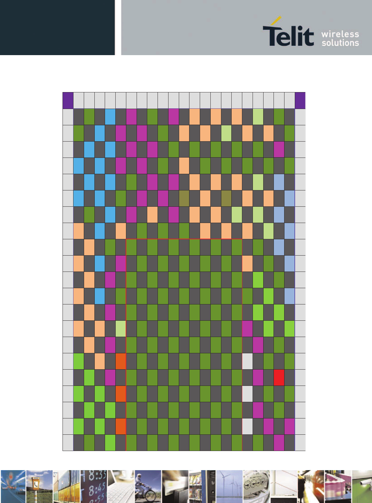
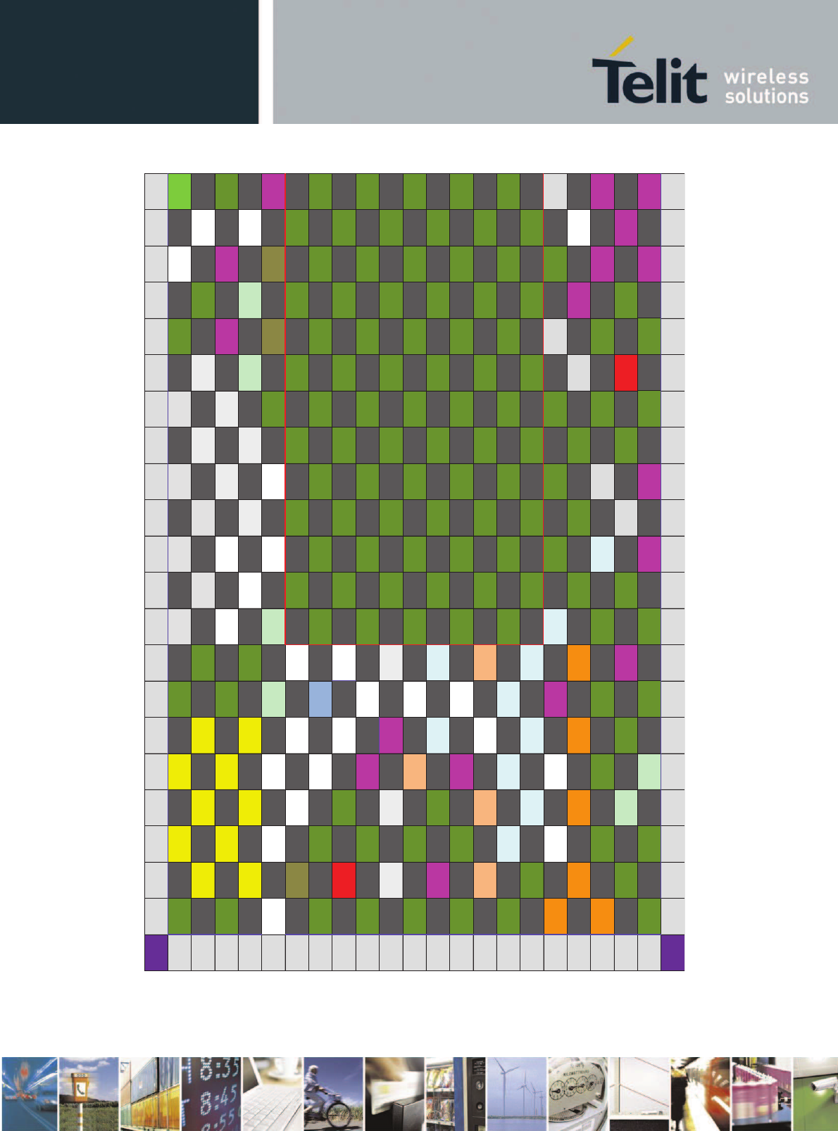
3.2. LGA Pads Layout
A B C D E F G H J K L M N P R S T U V W X
1GND GND SD_DAT0 SD_DAT1 SD_DAT2 SD_DAT3 SDIO_DAT0 GND GND RFU23
2GND RFU5 SD_CLK SD_CMD SD_CARD_DE
TGND SDIO_DAT1 GND ANT_GPS GND RFU21
3GPIO73_EINT1
0GND GPIO72_EINT9 CAM2_PD GND SDIO_DAT2 SDIO_CMD GND GND RFU17
4CAM1_PD GND CAM2_RESET CAM1_RESET GND SDIO_CLK SDIO_DAT3 RFU13 RFU14 RFU15 GND
5GPIO67_EINT0 GND GPIO66_EINT1
5GPIO65 GPIO54_EINT1 GND RFU12 USIF1_SCLK USIF1_CS USIF1_RXD
6GPIO64_EINT1
3GND GPIO63_EINT8 CAM1_TORCH GND GND GND GND GND GND GND
7CAM1_FLASH GND TP_RESET GPIO56 GND GND GND GND GND GND
8GPIO52_EINT1
5GND GPIO51 GPIO50 GND GND GND GND GND GND GND
9GPIO49 GND GPIO48 GPIO47 GND GND GND GND GND GND
10 GPIO46 GND GPIO45 GPIO44 GND GND GND GND GND GND GND
11 GPIO57_EINT9 GPIO58_EINT2 TP_IRQ GND GND GND GND GND GND GND
12 RFU28 GND RFU31 RFU30 GND GND GND GND GND GND GND
13 GND GND RFU33 GND GND GND GND GND GND GND
14 GND RFU26 RFU32 GPIO55_EINT1
5GND GND GND GND GND GND GND
15 RFU35 RFU34 RFU29 GND GND GND GND GND GND GND
16 RFU4 RFU3 GND RFU27 GND GND GND GND GND GND GND
17 RFU2 RFU1 GND GPIO53 RFU7 GND CAM_MCLK USB_DP USB_DN USB_ID
18 CSI2_DP CSI2_DN CSI1_DP3 CSI1_DN3 GND RFU39 RFU38 RFU37 RFU36 LVDS_TB1N
LVDS_TB1P
19 CSI2_CLKP CSI2_CLKN CSI1_DP2 CSI1_DN2 CSI1_DN1 CSI1_DP1 DSI_DN0 DSI_DP0 LVDS_TA1N LVDS_TA1P
20 GND CSI1_CLKP CSI1_CLKN GND DSI_DN2 DSI_DP2 DSI_DN1 DSI_DP1 LVDS_TC1N LVDS_TC1P GND
21 GND CSI1_DP0 CSI1_DN0 DSI_DN3 DSI_DP3 DSI_CLKP DSI_CLKN LVDS_TCLK1N LVDS_TCLK1P LVDS_TD1N
A B C D E F G H J K L M N P R S T U V W X
xE922-3GR Hardware User Guide
1VV0301272 Rev.0.8 2017-01-05
Reproduction forbidden without written authorization from Telit Communications S.p.A. - All Rights
Reserved. Page 38 of 112
Y AA AB AC AD AE AF AG AH AJ AK AL AM AN AP AR AS AT AU AV AW
RFU24 RFU25 GND GND RFU11 RFU10 GND GND AUX_I2C_SDA GND GND 1
RFU22 GND ANT_MAIN GND USIF2_CS GND RFU9 GND AUX_I2C_SCL GND 2
RFU18 RFU19 GND GND USIF2_RXD VSIM2 GND GND GND GND JTAG_RTCK 3
VAUX_3P0V RFU20 USIF2_TXD GND GND GND JTAG_TDI JTAG_TMS JTAG_TDO JTAG_TCK 4
USIF1_TXD GND USIF2_SCLK GND GND GND VSIM1 RFU16 HW_KEY
MAIN_RESET_I
NJTAG_TRST 5
GND GND GND GND GND GND SIMRST1 SIMCLK1 SIMIO1 GND 6
GND GND GND GND GND GND GND SIMRST2 SIMCLK2 SIMIO2 GND 7
GND GND GND GND GND GND GPIO7 VBUS_DET GPIO1_EINT2 GPIO0_EINT5 8
GND GND GND GND GND GND GND LCD_TE RFU8 GND GND 9
GND GND GND GND GND GND
USIM1_DETEC
T
USIM2_DETEC
TGND RFU44 10
GND GND GND GND GND GND GND LCD_RESET GPIO5_EINT7 GND GND 11
GND GND GND GND GND GND DIG_MIC_D1 RFU40 DIG_MIC_D2 DIG_MIC_CLK 12
GND GND GND GND GND GND GND LEDDRV RFU6 GND GND 13
GND GND GND GND GND GND CHG_RST_OU
TLED_CURSINK GND ANT_WIFI 14
GND GND GND GND GND GND GND VDD_SD CABC GND GND 15
GND GND GND GND GND GND CHG_POK_IN ON_OFF FG_IBATN FG_IBATP 16
RFU41 TP_SCL TP_SDA GND VAUX_2P85V 1V8_OUT CAM_I2C_SDA CAM_I2C_SCL LEDFB_DP LEDFB_DN
VBUS_PWR_E
N17
VAUX_1P8V CHG_I2C_SCL CHG_I2C_SDA MIC_VDD VMIC_BIAS ADC_IN0 GND V_BAT_1 V_BAT_PA_2 V_BAT_PA_1 18
GND RFU42 RFU43 MICP2 MICN2 ADC_IN1
ADC_VBATME
AS GND V_BAT_2 V_BAT_PA_3 GND 19
V_RTC GND MICN1 MICP1 HP_OUT_R HP_OUT_L GND V_BAT_3 V_BAT_4 V_BAT_5 20
LVDS_TD1P
CHG_INT_IN GND SPKR_LN SPKR_LP EP_P EP_N GND V_BAT_6 V_BAT_7 GND 21
Y AA AB AC AD AE AF AG AH AJ AK AL AM AN AP AR AS AT AU AV AW
xE922-3GR Hardware User Guide
1VV0301272 Rev.0.8 2017-01-05
Reproduction forbidden without written authorization from Telit Communications S.p.A. - All Rights
Reserved. Page 39 of 112
4. Electrical specifications
4.1. Absolute maximum ratings – not operational
A deviation from listed below values range may harm the xE922-3GR module.
Symbol
Parameter
Min
Max
Unit
VBATT
battery supply voltage on
pin VBATT
-0.3
+5.5
[V]
VBATT_PA
battery supply voltage on
pin VBATT_PA
-0.3
+6.0
[V]
4.2. Recommended operating conditions
Symbol
Parameter
Min
Typ
Max
Unit
Tcase
Case temperature (1)
-40
+25
+85
[°C]
VBATT
Battery supply voltage on
pin VBATT
3.6
3.8
4.2
[V]
VBATT_PA
Battery supply voltage on
pin VBATT_PA
3.6
3.8
4.2
[V]
IBATT_PA
+ I
BATT
Peak current to be used to
dimension decoupling
capacitors on pin
VBATT_PA
-
2
-
[A]
(1) Tcase case temperature: measured at top side shield of module
4.3. Logic Level Specifications
Unless otherwise specified, all the interface circuits of the xE922-3GR are 1.8V CMOS logic.
Only few specific interfaces (such as USIM) are capable of dual voltage I/O.
The following table shows the logic level specifications used in the Telit xE922-3GR
interface circuits:
NOTE:
Do not connect xE922-3GR’s digital logic signal directly to OEM’s digital logic signal with a
level higher than 2.1V for 1.8V CMOS signals.
xE922-3GR Hardware User Guide
1VV0301272 Rev.0.8 2017-01-05
Reproduction forbidden without written authorization from Telit Communications S.p.A. - All Rights
Reserved. Page 40 of 112
For 1.8V CMOS signals:
Absolute Maximum Ratings - Not Functional
Parameter
xE922-3GR
Min
Max
Input level on any
digital pin when on
-0.3V
+2.16V
Input voltage on
analog pins when on
-0.3V
+2.16 V
Operating Range - Interface levels (1.8V CMOS)
Parameter
xE922-3GR
Unit
condition
Min
Max
V
IH
Input high level
1.3V
2.1V
[V]
V
IL
Input low level
-0.3V
0.5V
[V]
V
OH
Output high level
1.6V
[V]
Ioh= 0.1 mA
V
OL
Output low level
0.2V
[V]
Ioh = -0.1mA
IIL
Low-level input current
1.5
[µA]
no PU/PD
IIH
High-level input current
1.3
[µA]
no PU/PD
RPU/PD
pull up/down resistance
7.2
45
[kΩ]
I_source/sink
GPIO drive strength
2
12
[mA]
Configurable 2,4,8,12 mA
Vdrv_HIGH=1.62V/LOW=0.18V
xE922-3GR Hardware User Guide
1VV0301272 Rev.0.8 2017-01-05
Reproduction forbidden without written authorization from Telit Communications S.p.A. - All Rights
Reserved. Page 41 of 112
5. Power supply
5.1. Input supply
There are 2 input power supplies defined on the xE922-3GR module,
V_BAT, V_BAT_PA.
V_BAT_PA pin supplies transmit RF front end (RFFE) power amplifiers (PA) of the cellular network
(2G/3G) connection feature of the module.
V_BAT pin supplies the remaining module circuitry, distributed via an internal power management unit
(PMU).
Although defined separately, V_BAT and V_BAT_PA can be connected together. The split implementation
allows for separate power consumption characterization of the RFFE as well as optional noise filtering
network to isolate V_BAT from the typical bursty character of V_BAT_PA in 2G mode operation.
NOTE:
In GSM
/GPRS mode, RF transmission is not continuous and is packed into bursts at a base
frequency of about 216 Hz with relative current peaks as high as about 2 A.
Therefore the power
supply must be designed to withstand these current peaks
(from V_BAT_PA input supply pin)
without big voltage drops; this means that both the electrical design
(current rating and/or
decoupling buffer capacitors)
and the board layout must be designed for this current flow. If
the layout of the PCB is not well
designed, a strong noise floor is generated on the ground. This
will reflect on all the audio paths producing an audible annoying noise at 216 Hz; if the voltage
drops during the peaks, current absorption is too high. The device may even shut down as a
consequence of the supply voltage drop.
xE922-3GR Hardware User Guide
1VV0301272 Rev.0.8 2017-01-05
Reproduction forbidden without written authorization from Telit Communications S.p.A. - All Rights
Reserved. Page 42 of 112
Both V_BAT_PA and V_BAT are protected by Zener transient voltage suppressor diodes internal the module.
Although the internal transient suppressor also protects for reverse polarized input supply application, its max
power dissipation is limited as well.
For performance specification of this protection please consult the datasheet. (DF3A6.8FUT1 / ON
Semiconductor)
A low ESR buffer capacitor of adequate capacity must be provided on the application main board in order to
cut the current absorption peaks (either from system load or during cellular load TX slots , up to 2 A), taking
into account the sourcing power supply circuitry implementation is limited qua current rating and/or transient
response timing. The buffer capacitor must be selected in order to guarantee at all time V_BAT > BUV
battery under voltage (typical 3.0V).
For information, the total ‘distributed’ capacitance already present inside the module:
· V_BAT_PA : 33uF
· V_BAT : 82uF
5.2. Output supply
5.2.1. Linear voltage regulators
5.2.1.1. VAUX_1P8V
parameter
symbol
value
unit
condition
Default
value
Default
state
Min
Typ
max
External
cappacitor
Cext
1000
1400
nF
Cappacitor
ESR
R_esr
100
ohm
100 Hz
0.05
ohm
1 MHz…30MHz
Output vo
l
tage
Vreg
1.8
2.85
V
Configurable
1.8/2.5/2.8/2.85V
2.85V
OFF
Output
Current
Ireg
max
225
mA
Current
Limitation
Ima
x
400
mA
50% nominal
LDO voltage
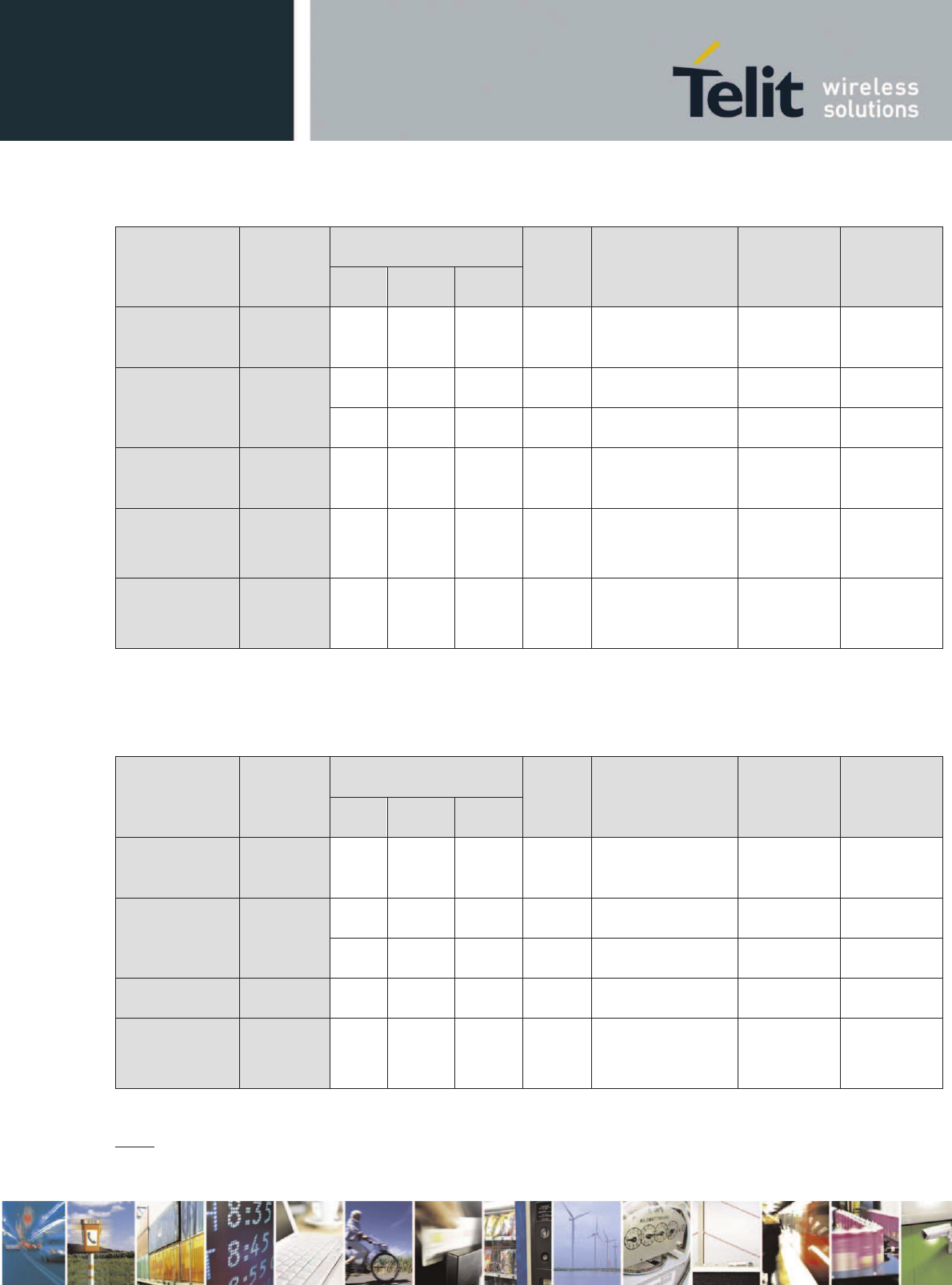
xE922-3GR Hardware User Guide
1VV0301272 Rev.0.8 2017-01-05
Reproduction forbidden without written authorization from Telit Communications S.p.A. - All Rights
Reserved. Page 43 of 112
5.2.1.2. VAUX_2P85V
parameter
symbol
value
unit
condition
Default
value
Default
state
Min
Typ
max
External
cappacitor
Cext
1000
1400
nF
Cappacitor
ESR
R_esr
100
ohm
100 Hz
0.05
ohm
1 MHz…30MHz
Output vo
l
tage
Vreg
1.8
2.85
V
Configurable
1.8/2.5/2.8/2.85V
2.85V
OFF
Output
Current
Ireg
max
225
mA
Current
Limitation
Ima
x
400
mA
50% nominal
LDO voltage
5.2.1.3. VAUX_3P0V
parameter
symbol
value
unit
condition
Default
value
Default
state
Min
Typ
max
External
cappacitor
Cext
1000
nF
Cappacitor
ESR
R_esr
100
ohm
100 Hz
0.05
ohm
1 MHz…30MHz
Output vo
l
tage
Vreg
3.0
V
ON
Current
Limitation
Imax
1
A
V_BAT>3.5V
Note:
VAUX_3P0V is also applied internally the module, feeding the flash memory part of the eMCP memory.
xE922-3GR Hardware User Guide
1VV0301272 Rev.0.8 2017-01-05
Reproduction forbidden without written authorization from Telit Communications S.p.A. - All Rights
Reserved. Page 44 of 112
The datasheet of the eMCP specifies a maximum current consumption on this powersupply line of about
150mA (read operation).
Care should be exercised to limit the total power consumption, to keep heat dissipation limited:
Power_dissipation = (V_BAT-3.0V) x (150mA_max+I_external)
5.2.1.4. VSIM1/2
parameter
symbol
value
unit
condition
Default
value
Default
state
Min
Typ
max
External
cappacitor
Cext
100
135
nF
Cappacitor
ESR
R_esr
100
ohm
100 Hz
0.05
ohm
1 MHz…30MHz
Output vo
l
tage
Vreg
1.2
2.91
V
2.91V
ON
Output
Current
Ireg
max
30
mA
Current
Limitation
Imax
80
mA
5.2.2. DC/DC stepdown
5.2.2.1. 1V8_OUT
parameter
symbol
value
unit
condition
Default
value
Default
state
Min
Typ
max
Output capacitor
C
out
11
22
+35%
u
F
internal module
tot.cap
+/-
32 uF
Capacitor ESR
R_esr
100
ohm
100 Hz
0.05
ohm
1 MHz…
1
0MHz
Output vo
ltage
Vreg
1.8
V
1.8V
ON
Output
Ireg
1.2
A
xE922-3GR Hardware User Guide
1VV0301272 Rev.0.8 2017-01-05
Reproduction forbidden without written authorization from Telit Communications S.p.A. - All Rights
Reserved. Page 45 of 112
Current
max
Pull
-downr r
esistor
Rpd
200
ohm
DC/DC is OFF
Switching
frequency
F_dcdc
-3%
3.2
+3%
MHz
Note:
1V8_OUT is also applied internally the module feeding several I/O peripherals, memory interface and analog
RF parts (depending on use case).
Care should be exercised to keep external current dissipation limited in order not to exceed the maximum
output current of the DC/DC regulator.
1V8_OUT external usage is primarily targeted for IO reference level or supplying levelshift devices.
5.3. Typical system power consumption
Test conditions:
· room temperature 22deg, still air, no heatsink
· V_BAT/V_BAT_PA= 3.8V
· 50 ohm antenna load impedance
· Display and camera supply current excluded (separately powered)
WLAN related use cases are executed with WiFi hotspot serving the DUT as only client, inside RF shield box.
These are typical power consumption measured at room temperature, with the module mounted on Telit’s
reference carrier board, no heatsink applied.
At higher ambient temperature condition one can expect higher current consumption due to increasing leakage
currents.
SW release: MR1 // sf3gr_telit_he922-flashfiles-eng.android_a60_ww33_camera_orientation.
Type
description
[mA]
off
Module powered off
0.15
idle
Idle Display On
200
WLAN Active Idle
(3G cell registered)
18
3G Active Idle
21
xE922-3GR Hardware User Guide
1VV0301272 Rev.0.8 2017-01-05
Reproduction forbidden without written authorization from Telit Communications S.p.A. - All Rights
Reserved. Page 46 of 112
standby
Flight Mode
2.6
WLAN Idle associated
(3G cell registered)
8.6
2G
Standby, DRX5
GSM850
4.8
GSM900
4.8
DCS1800
4.8
PCS1900
6.3
3G Standby, DRX7
B1
4
B2
4.7
B5
4.1
B8
4.1
Data traffic
GPRS 4TX(gamma10)/1RX PS
GSM850
212
GSM900
220
DCS1800
173
PCS1900
185
3G 24dBm RMC 12.2kbps
B1
572
B2
713
B5
480
B8
600
Audio Playback
MP3 Playback, Wired Headset, flight mode
103
Video Playback
Video Playback
720p 30fps H.264, HP level 4.0, 4
Mb/s,
Airplane Mode, Landscape Mode
345

xE922-3GR Hardware User Guide
1VV0301272 Rev.0.8 2017-01-05
Reproduction forbidden without written authorization from Telit Communications S.p.A. - All Rights
Reserved. Page 47 of 112
Video Streaming HTML5 WLAN
-H.264 -720p
776
Video Streaming HTML5
3G -H.264 -720p chrome52
959
Browsing
Browsing Chrome HTML5
-WLAN
44
8
Browsing Chrome HTML5
-3G
560
Imaging
User mode image capture, 3G idle
TBD
Video Recording, H
D 720p 30fps AVC baseline 3.1,
1.5Mbps, 3G idle
876
GNSS
Tracking mode (non
-assisted) :
GPX Logger app (typical
driving test)
, airplane mode
140
Acquisitioning mode
(non-assisted) 8 satellites / -
130dBm
TBD
Tracking mode (non
-assisted) 8 satellites / -130dBm
TBD
BT
Upload file sending
460
Download file
receiving
535
BT enabled , no device connected
3
1 BLE sensor device connected, no data
4.6
1 BLE sensor notifying @1second period
84
1 BLE sensor notifying @5second period
37
6 BLE sensors device connected, no data
10
6 BLE sensors notifying
@1second period
89
6 BLE sensors notifying @5second period
86
5.4. RTC backup
The internal PMU features real-time clock (RTC) based on 32 kHz oscillator, to keep track of date and time.
This feature is supplied by an internal LDO V_RTC, typical 2.3V +-5%.
V_RTC is ‘always on’ when V_BAT supply is present (>2.5V min).
V_RTC is internally decoupled with 100 nF. When V_BAT is removed from the module, in case RTC
tracking is needed an external supercap is required connected to module pin V_RTC.

xE922-3GR Hardware User Guide
1VV0301272 Rev.0.8 2017-01-05
Reproduction forbidden without written authorization from Telit Communications S.p.A. - All Rights
Reserved. Page 48 of 112
The following table gives an overview of V_RTC minimum voltage level requirements in order to keep RTC
running:
condition
minimum V_RTC [V]
min Typ max
room temp
erature
0.8
1.1
-40 to +125deg
0.9
1.2
So typically at room temperature a voltage difference of 2.3V – 0.8V = 1.5V is available for buffering the
RTC supply in case V_BAT is removed.
An external capacitor for RTC buffering can be added, typical 100uF, up to maximum 220uF directly to the
LGA pin V_RTC.
In case an extreme large (super) capacitor, typical 1 F, is applied, a series resistor of typical 470 Ohm should
be added.
Typical current drawn from V_RTC by the RTC clock: 2.6µA
An RTC alarm is one of the possible events to power ON the module.
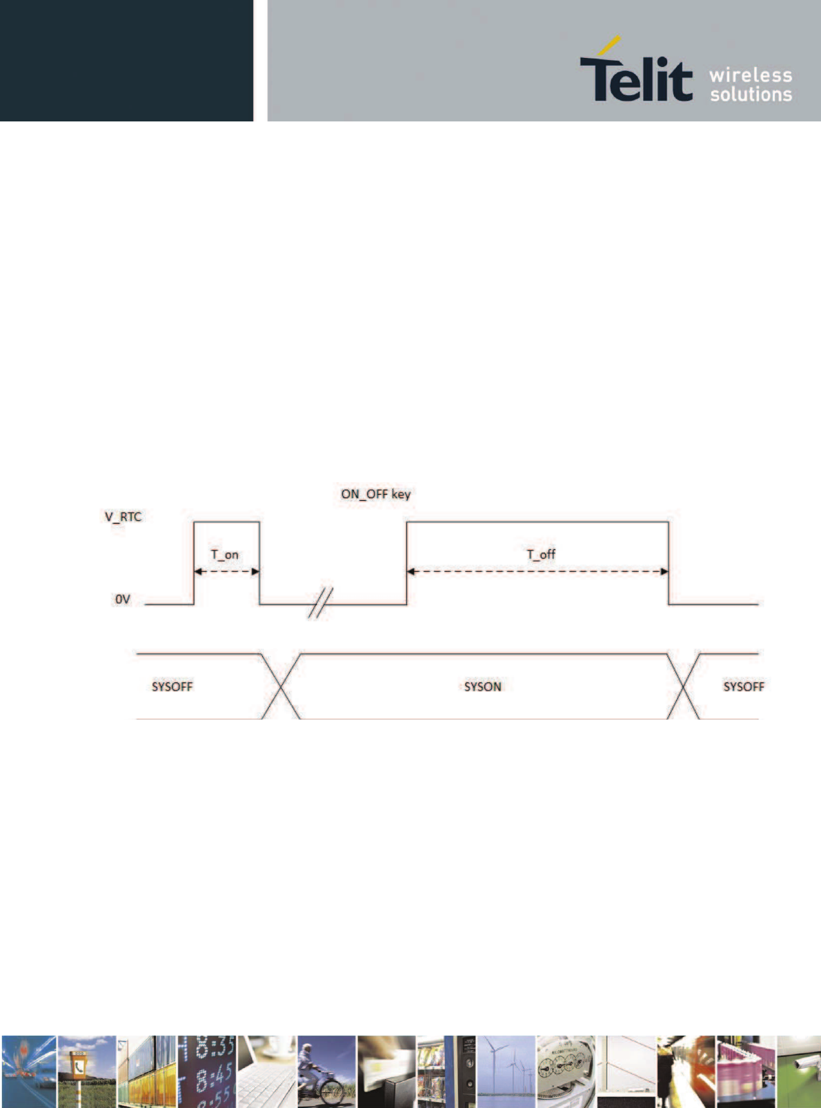
xE922-3GR Hardware User Guide
1VV0301272 Rev.0.8 2017-01-05
Reproduction forbidden without written authorization from Telit Communications S.p.A. - All Rights
Reserved. Page 49 of 112
6. Power ON/OFF and reset control
6.1. Power On
Once power applied to the V_BAT, the power on can be triggered by four possible events:
· ON_OFF key event (+ application of power to system with ‘first connect’ enabled)
· External charger detection (CHG_POK)
· RTC alarm
6.1.1. ON_OFF key action
If the ON_OFF key is forced by external circuitry to V_RTC, the sytem startup procedure begins.
· Active logic : HIGH
· T_on minimum : 100msec
· Debounce :15msec
When the system is supplied with V_BAT for the first time, it will automatically start up without waiting for
an event.
This so called ‘first connect’ power up condition can be disabled by adding a pulldown resistor on ON_OFF
signal of typical 10 kOhm.
Once the system is ON, if the ON_OFF key is forced to V_RTC for minium T_off > 10 seconds, the system
will switch OFF again.
After the initial startup procedure and when FW has booted, the ON_OFF key will be re-programmed to wake
up the system when asserted during sleep mode.

xE922-3GR Hardware User Guide
1VV0301272 Rev.0.8 2017-01-05
Reproduction forbidden without written authorization from Telit Communications S.p.A. - All Rights
Reserved. Page 50 of 112
6.1.2. Switching ON due to charging
If an external charger is detected the system startup procedure begins. An external charger can be detected by
LOW level detection on CHG_POK and / or CHG_INT input pins. Both pins have an internal pullup applied
to V_RTC. (See chapter 7.2 for charger IC connections)
6.1.3. Switching on due to RTC alarm
The real time clock can generate a wake-up signal called RTC alarm. Once the PMU detects this level high
the system startup procedure begins.
6.2. Power off
There are two ways to trigger a power off cycle of the system.
6.2.1. Soft power off
Based on application specific implementation and/or user interaction, the SW can trigger a power off cycle.
6.2.2. Emergency power off
In case the PMU detects a HW failure, the PMU will shut down by itself.
The following events will trigger an emergency power off:
· PMU watchdog time-out
· ON_OFF key pressed for more than 10 sec
· ADC_VBATMEAS < threshold ( default 2.3V)
Overtemperature (refer to thermal design guide)
6.3. Reset
For soft reset, the system SW can trigger two types of soft reset.
One type will reset the DBB and go through the PMU power off/on sequence,
The other type will only reset the CPU while keeping voltage regulators enabled.
For hard reset, the system can be reset by pulling LGA pin AU5 “MAIN_RESET_IN” active LOW.
xE922-3GR Hardware User Guide
1VV0301272 Rev.0.8 2017-01-05
Reproduction forbidden without written authorization from Telit Communications S.p.A. - All Rights
Reserved. Page 51 of 112
7. Battery management
The xE922-3GR chipset supports an (optional) complete battery management solution based on external
charger IC interfacing by the following dedicated charging control lines.
PAD
Signal
I/O
descriptions Type
AN14
CHG_RST_OUT
O
External Charger Reset
AB21
CHG_INT_IN
I
Charger IRQ
AN16
CHG_POK_IN
I
Charger Power OK indication
AV16
FG_IBATP
I
Battery Fuel Gauge Positive
AT16
FG_IBATN
I
Battery Fuel Gauge Negative
AM19
ADC_VBATMEAS
I
Battery measurement ADC
AC18
CHG_I2C_SCL
I/O
Charger I2C Clock
CMOS 1.8V
AE18
CHG_I2C_SDA
I/O
Charger I2C Data
CMOS 1.8V
AL18
ADC_IN0
AI
Analog to Digital converter (MEAS0 Batt ID)
Analog
AK19
ADC_IN1
AI
Analog to Digital converter (MEAS1 Batt Temp)
Analog
The battery management system foresees in the following main functions:
· Battery voltage/capacity monitoring (fuel gauge)
· Battery charger interface (I2C bus, predefined IO’s)
7.1. Coulomb counter
The coulomb counter is a current integration method to improve the battery state of charge, while combined
with VBATMEAS voltage monitoring. Below figure shows the required connections, where the biderectional
battery current is sensed across a shunt resistor (low side sensing, typ. 20 mOhm).
Always connect the sense resistor to the negative (ground) side of the battery. Positive side battery sensing is
not supported and will damage the chip.
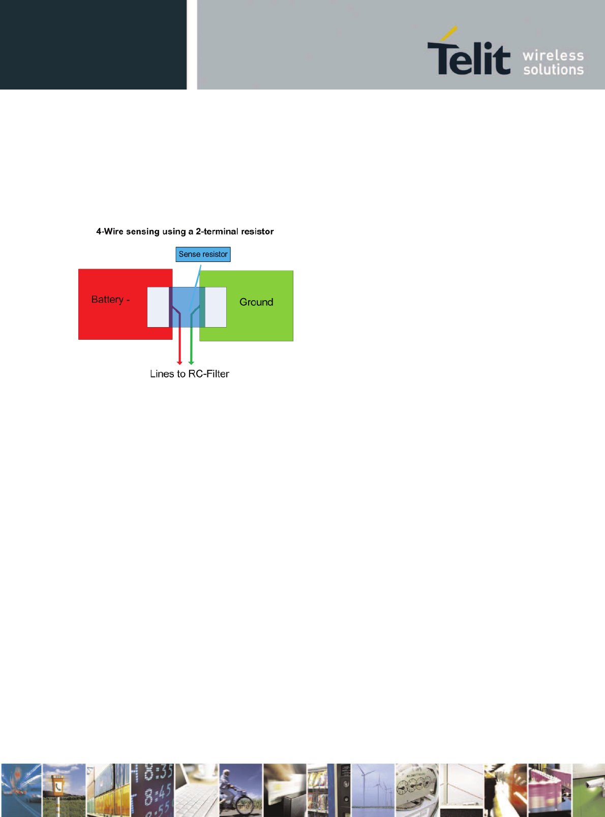
xE922-3GR Hardware User Guide
1VV0301272 Rev.0.8 2017-01-05
Reproduction forbidden without written authorization from Telit Communications S.p.A. - All Rights
Reserved. Page 52 of 112
Minimize parasitic resistance in the current path by using thick copper traces between sense resistor and PCB
ground and negative battery terminal respectively.
The fuel gauge FG_IBATP/N signal pair should be routed as differential and isolated from aggressors (like
clocks, DC/DC switching nodes) to minimize noise interference.
A low pass filter 4.7k/1uF is present inside the xE922-3GR module.
When using 2-teminal resistor, apply 4-wire terminal layout pattern scheme as suggested in following figure.
7.2. Battery charging
The system SW supports application of an external charger IC solution BQ24296 from Texas Instruments TI,
an I2C controlled, 3A single cell, USB Charger. For detailed performance, please consult the datasheet.
Please consult Intel’s IBL support website for application note and actual supported charger IC type numbers.
7.2.1. Block diagram
The below figure gives an overview how the BQ24296 solution should be interfaced with the onboard
PMU/ABB/DBB functions.
Note: currently PSEL control from ABB is not supported. Charging from USB or DC-adapter is set by tying
PSEL to HIGH or LOW respectively.
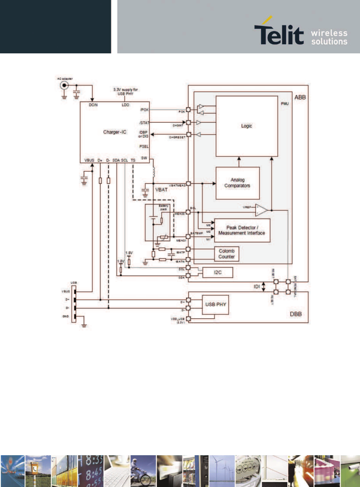
xE922-3GR Hardware User Guide
1VV0301272 Rev.0.8 2017-01-05
Reproduction forbidden without written authorization from Telit Communications S.p.A. - All Rights
Reserved. Page 53 of 112
The CHG_POK line (active LOW, internal pullup to always_on domain V_RTC) wakes the system once a
valid input supply source is present. It has the same effect as the ON_OFF key event to initiate a power-up
sequence.
The CHG_INT line (active LOW, internal pullup to always_on domain V_RTC) signals charger state change
or failure, and replaces, in case not used, the CHG_POK function.
The CHG_RESET will disable the external charger, in case of PMU reset or battery removal detect.
The CHG_I2C interface is used to control charging process parameters and charger status monitoring.
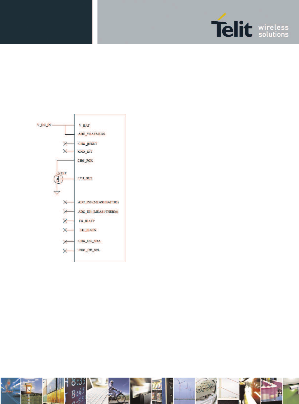
xE922-3GR Hardware User Guide
1VV0301272 Rev.0.8 2017-01-05
Reproduction forbidden without written authorization from Telit Communications S.p.A. - All Rights
Reserved. Page 54 of 112
7.2.2. Battery/charger-less operation
In case the xE922-3GR module is applied directly from a DC source supply, without battery and/or external
charger IC, the charger specific interface signals should be connected as indicated in the next picture.
Since VBATMEAS and POK signals are still used in the power on sequencing / boot process, it is important
to have the following minimum connections implemented.
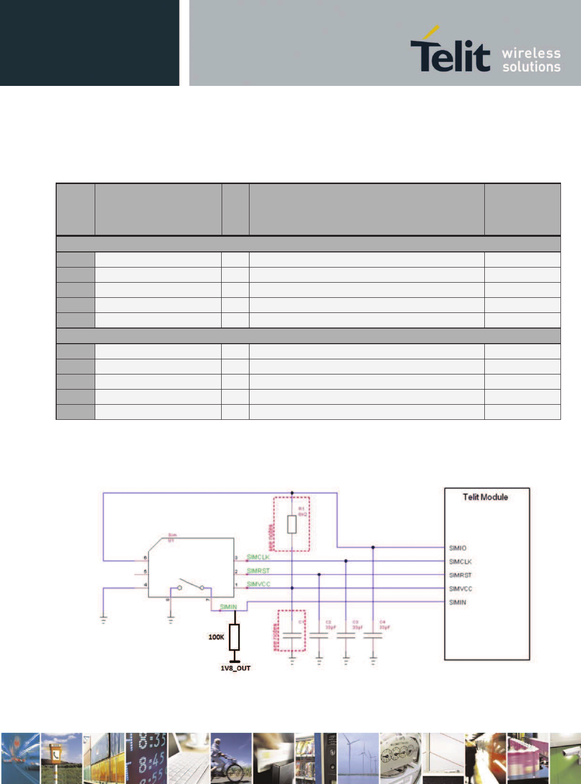
xE922-3GR Hardware User Guide
1VV0301272 Rev.0.8 2017-01-05
Reproduction forbidden without written authorization from Telit Communications S.p.A. - All Rights
Reserved. Page 55 of 112
8. USIM interface
xE922-3GR supports two external USIM interfaces (dual volt 1.8/3V) compatible with ISO
7816-3 IC Card standard.
PAD
Signal
I/O
descriptions Type
SIM card interface 1
AM5
VSIM1
-
External SIM signal 1 – Power supply for the SIM
1.8 / 2.85V
AR6
SIMCLK1
O
External SIM signal 1 – Clock
1.8 / 2.85V
AN10
USIM1_DETECT
I
External SIM signal 1 – Card detect (Active low)
CMOS 1.8V
AT6
SIMIO1
I/O
External SIM signal 1 – Data I/O
1.8 / 2.85V
AN6
SIMRST1
O
External SIM signal 1 – Reset
1.8 / 2.85V
SIM card interface 2
AK3
VSIM2
-
External SIM signal 2 – Power supply for the SIM
1.8 / 2.85V
AS7
SIMCLK2
O
External SIM signal 2 – Clock
1.8 / 2.85V
AR10
USIM2_DETECT
I
External SIM signal 2 – Card detect (Active low)
CMOS 1.8V
AU7
SIMIO2
I/O
External SIM signal 2 – Data I/O
1.8 / 2.85V
AP7
SIMRST2
O
External SIM signal 2 – Reset
1.8 / 2.85V
Next figure illustrates how a typical SIM socket should be connected.

xE922-3GR Hardware User Guide
1VV0301272 Rev.0.8 2017-01-05
Reproduction forbidden without written authorization from Telit Communications S.p.A. - All Rights
Reserved. Page 56 of 112
NOTE FOR R1:
The resistor value on SIMIO pulled up to SIMVCC should be defined accordingly in order to
be compliant with 3GPP specification for USIM electrical testing. Rise/fall time of SIMIO line
should not exceed 1 µs.
The xE922-3GR module contains an internal 4.7 kOhm pull-up resistor on SIMIO which should
be sufficient in most applications.
For C1 a value of 1uF is recommended with the XE922-3GR product.
USIMx_DETECT line has no internal pull up activated, an external pullup resistor of typical
100 kOhm is required on the application main board.
Refer to the following document for more SIM integration recommendations:
· SIM_Integration_Design_Guide_Application_Note_Rev10, 80000nt10001a
Note1:
Only SIM1 interface is active by default.
Please consult Intel Business Link Support (IBL) how to activate SIM2 interface
Note2:
USIM_DETECT mechanism is not enabled by default.
SIM detection is currently implemented via SW polling.
Please consult Intel Business Link Support (IBL) on HW SIM detection.
xE922-3GR Hardware User Guide
1VV0301272 Rev.0.8 2017-01-05
Reproduction forbidden without written authorization from Telit Communications S.p.A. - All Rights
Reserved. Page 57 of 112
9. USB port
The xE922-3GR module includes a Universal Serial Bus (USB) transceiver, which operates at
USB high-speed (480Mbits/sec). It can also operate with USB full-speed (12Mbits/sec) hosts.
It is compliant with the USB 2.0 ‘DRD’ dual role specification, 15 endpoints, and can be used
control and data transfers as well as for diagnostic monitoring and firmware update.
The interface does not support ‘OTG’ (HNP) to switch roles on the fly.
Once the module enumerates as a device or host, it stays in that mode. The USB cable needs to
be removed and reconnected to enumerate in the alternate mode.
The USB port on the Telit xE922-3GR is typically the main interface between the module and
OEM hardware.
The USB_D+ and USB_D- signals have a clock rate of 480MHz in HS mode. The signal traces
should be routed carefully. Trace lengths, number of vias and capacitive loading should be
minimized. The impedance value should be as close as possible to 90 Ohms differential.
The table below describes the USB interface signals:
For proper DRD operation USB_ID (W17) should be connected to GPIO1_EINT2 (AT18) to
detect device connection in low power modes.
NOTE:
- VBUS_DET input power is internally used to detect cable VBUS (USB device attach) and
start enumeration process. It is not used for supplying internal xE922-3GR USB HW block.
NOTE:
In the case of not using USB communication, it is still highly recommended to place an optional
USB connector in the application board.
Signal
xE922-3GR Pad.
Usage
VBUS_DET
AR8
Power sense for the internal USB transceiver.
Minimum high level detect level @ roomtemp: 2.9V
USB_D
-
U17
Minus (-) line of the differential, bi-directional USB
signal to/from the peripheral device
USB_D+
S17
Plus (+) line of the differential, bi-directional USB
signal to/from the peripheral device
USB_ID
W17
ID pin to distinguish between host and device side for
dual role
DRD USB protocol
GPIO1_EINT2
AT8
Used for SoC USB ID WU from Sleep
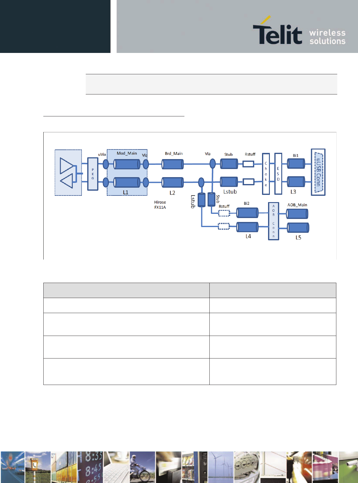
xE922-3GR Hardware User Guide
1VV0301272 Rev.0.8 2017-01-05
Reproduction forbidden without written authorization from Telit Communications S.p.A. - All Rights
Reserved. Page 58 of 112
At least Test point of the USB signals are required since the USB physical communication is
needed in the case of SW update.
Routing guide lines for the display USB2.0 interface:
The next figure shows a typical signal traject with different sub trajects.
Recommended routing guidelines for the whole USB signal traject :
parameter
guideline
Characteristic impedance (stripline / microstrip)
90 ohm differential 10%(SL) 15%(MS)
Trace spacing : between differential pairs or between
differential pair and other signals
(h = dielectric height)
4xh (SL) 6xh (MS)
Max. number of vias allowed
3 through
-
hole vias + 4 microvias (including
via under USB connector)
Length matching between P and N within a differential pair
Within same layer mismatch: +/
-
0.254 mm
Total length m
ismatch: +/-0.381 mm
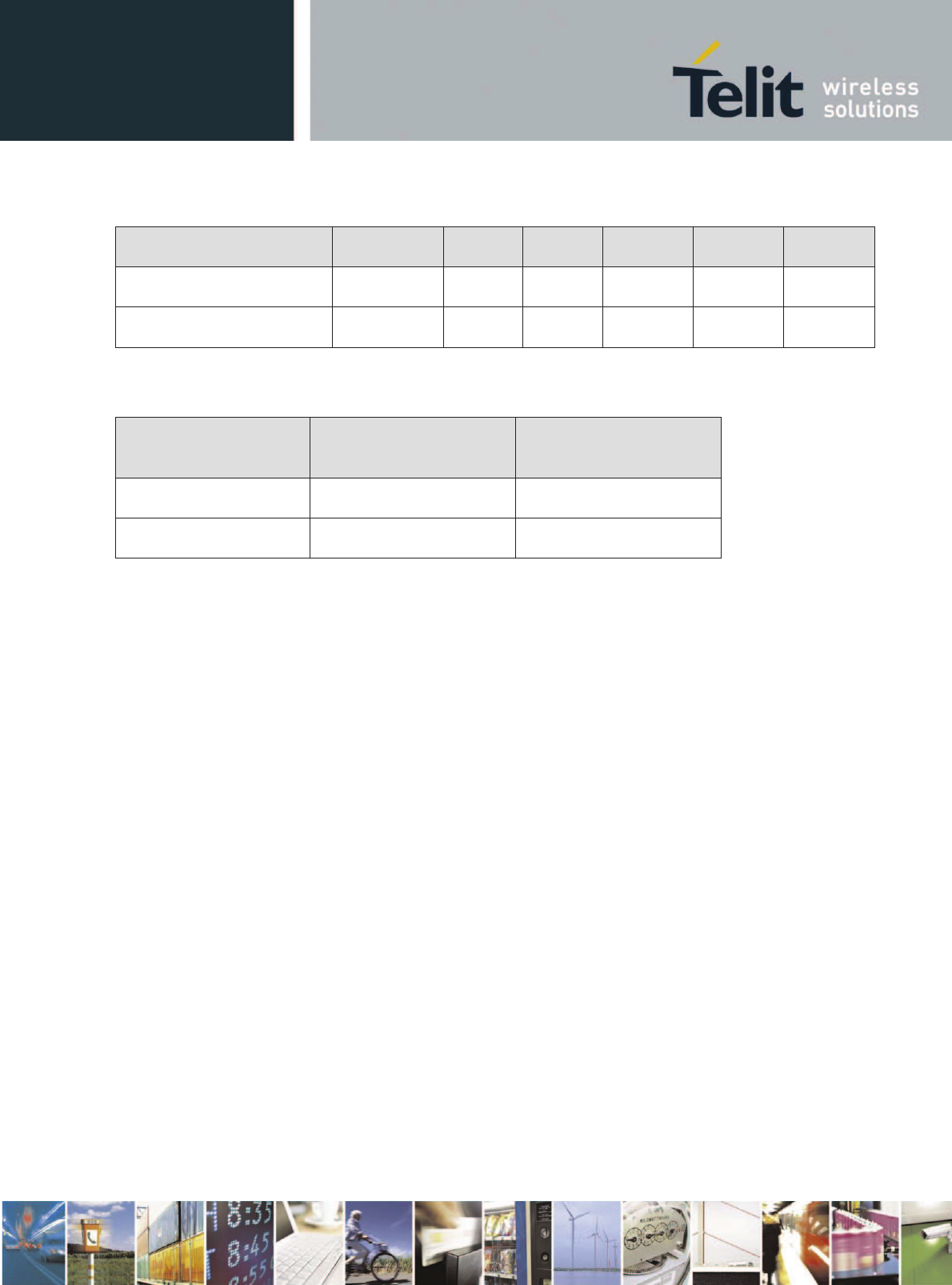
xE922-3GR Hardware User Guide
1VV0301272 Rev.0.8 2017-01-05
Reproduction forbidden without written authorization from Telit Communications S.p.A. - All Rights
Reserved. Page 59 of 112
Guidelines for sub trajects:
parameter
module
main
Bi1
Bi2
AOB
stub
Transmission line segment
L1 (MS/SL)
L2 (SL)
L3 (MS)
L4 (MS)
L5(SL)
Lstub
Max. length [mm]
25.4
101.6
12.7
25.4
101.6
5.1
Actual xE922-3GR module signal trace (L1) implementation:
signal name
module
trace length
[mm]
Number of microvias on
the module
USB_DP
5.06
3
USB_DN
5.29
3
xE922-3GR Hardware User Guide
1VV0301272 Rev.0.8 2017-01-05
Reproduction forbidden without written authorization from Telit Communications S.p.A. - All Rights
Reserved. Page 60 of 112
10. Display interface
The xE922-3GR supports a display according following 3 interface types:
· MIPI-DSI (4-lane, GPIO’s including tearing effect timing control)
· LVDS (4-lane)
On top of this display interface the module also features backlight control (CABC input, BL feedback input, BL
drive output) and I2C port to control a touch panel IC.
LCD_RESET and LCD_TE interface pins become available as general GPIO function in case no LCD feature
implemented in the system.
Please consult Intel’s IBL Support website for AVL (approved vendor list), as well for recommended
implementation and port assignment
10.1. MIPI-DSI
4-lane MIPI DSI compliant, utilizing MIPI DPHY as physical layer.
Max rate of bit clock of a DPHY lane is defined as 400MHz, or equivalent data rate 800Mbps.
PAD
Signal
I/O
descriptions Type
MIPI DSI Display Interface
S19
DSI_DP0
AO
LCD DSI Data_0 Positive
Analog
P19
DSI_DN0
AO
LCD DSI Data_0 Negative
Analog
R20
DSI_DP1
AO
LCD DSI Data_1 Positive
Analog
N20
DSI_DN1
AO
LCD DSI Data_1 Negative
Analog
L20
DSI_DP2
AO
LCD DSI Data_2 Positive
Analog
J20
DSI_DN2
AO
LCD DSI Data_2 Negative
Analog
K21
DSI_DP3
AO
LCD DSI Data_3 Positive
Analog
H21
DSI_DN3
AO
LCD DSI Data_3 Negative
Analog
M21
DSI_CLKP
AO
LCD DSI Clock Positive
Analog
P21
DSI_CLKN
AO
LCD DSI Clock Negative
Analog
AP11
LCD_RESET
I/O
LCD Reset / GPIO
CMOS 1.8V
AP9
LCD_TE
I/O
LCD Tearing effect input
CMOS 1.8V
Routing guide lines for the display MIPI-DSI interface:
The next figure shows a typical signal traject with different sub trajects.
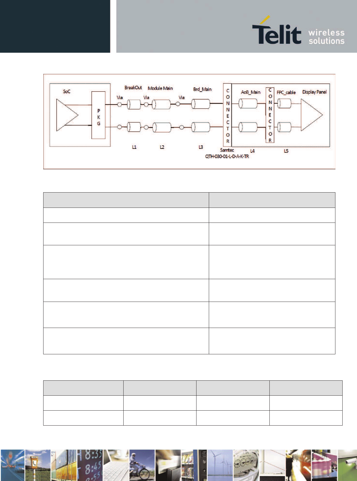
xE922-3GR Hardware User Guide
1VV0301272 Rev.0.8 2017-01-05
Reproduction forbidden without written authorization from Telit Communications S.p.A. - All Rights
Reserved. Page 61 of 112
Recommended routing guidelines for the whole MIPI-DSI signal traject:
parameter
guideline
Characteristic impedance (stripline
/ microstrip)
100 ohm differential 10%(SL) 15%(MS)
Trace spacing : between differ
e
ntial pairs or between
differential pair and other signals (h = dielectric height)
5xh (SL) 7xh (MS)
Total length
(module
(L1+L2) + carrier(L3)+add-on pcb(L4)
+ FPC
cable
(L5))
Min. 50.8 mm / Max. 152.4 mm
(MS/SL)
Max. n
umber of vias allowed
4 through
-
hole vias + 4 microvias + 2
connector pins
Length matching between P and N within a differential pair
Within same layer
mismatch: +/-
0.254 mm
Total length mismatch: +/
-0.381 mm
Length matching between DATA to CLK
Within same layer mismatch : +/
-
1.27 mm
Total length mismatch: +/
- 2.54 mm
Guidelines for off-module sub trajects:
parameter
Carrier board
Addon board
FPC
cable
Transmission line segment
L3
L4
L5
Length [mm]
50.8
- 83.8 (MS/SL)
12.7
- 25.4 (MS)
50.8
- 127
xE922-3GR Hardware User Guide
1VV0301272 Rev.0.8 2017-01-05
Reproduction forbidden without written authorization from Telit Communications S.p.A. - All Rights
Reserved. Page 62 of 112
Actual xE922-3GR module signal trace (L1+L2) implementation:
signal name
module
trace length
[mm]
Number of microvias on
the module
DSI_CLKN
9.88
2
DSI_CLKP
9.65
2
DSI_DN0
7.39
2
DSI_DP0
7.15
2
DSI_DN1
9.09
2
DSI_DP1
9.28
2
DSI_DN2
8.60
2
DSI_DP2
8.43
2
DSI_DN3
12.16
2
DSI_DP3
12.01
2
10.2. LVDS
4-lane ‘Low voltage differential signaling’ LVDS transmitter, implementing the LVDS PHY with electrical
parameters according TIA/EIA-644 technical standard.
LVDS Clock range: 20 – 170 MHz.
PAD
Signal
I/O
descriptions Type
LVDS Display Interface
W19
LVDS_TA1P
AO
LVDS Data A Positive
Analog
U19
LVDS_TA1N
AO
LVDS Data A Negative
Analog
X18
LVDS_TB1P
AO
LVDS Data B Positive
Analog
V18
LVDS_TB1N
AO
LVDS Data B Negative
Analog
V20
LVDS_TC1P
AO
LVDS Data C Positive
Analog
T20
LVDS_TC1N
AO
LVDS Data C Negative
Analog
Y21
LVDS_TD1P
AO
LVDS Data D Positive
Analog
W21
LVDS_TD1N
AO
LVDS Data D Negative
Analog
U21
LVDS_TCLK1P
AO
LVDS Clock Positive
Analog
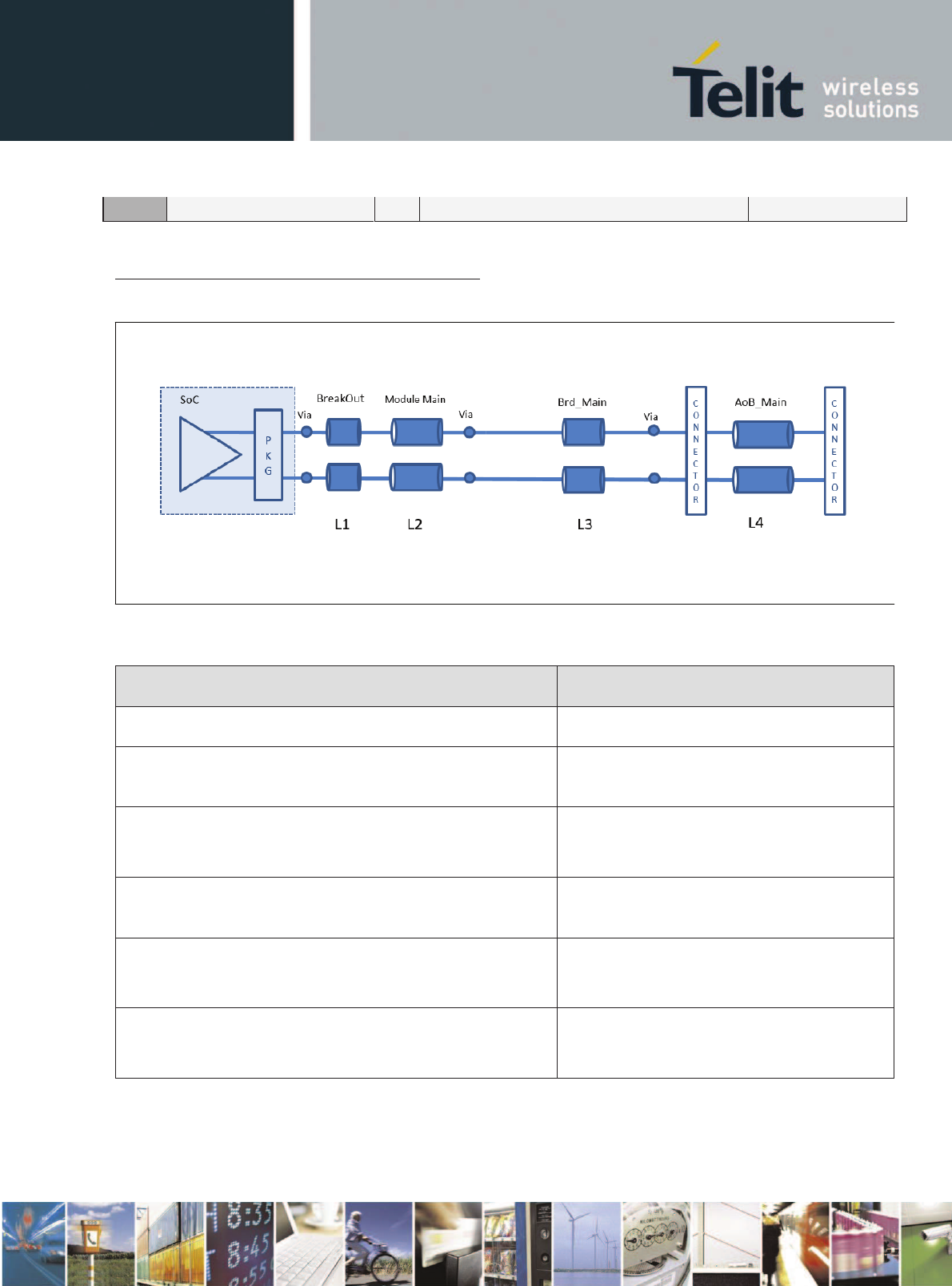
xE922-3GR Hardware User Guide
1VV0301272 Rev.0.8 2017-01-05
Reproduction forbidden without written authorization from Telit Communications S.p.A. - All Rights
Reserved. Page 63 of 112
S21
LVDS_TCLK1N
AO
LVDS Clock Negative
Analog
Routing guide lines for the display LVDS interface:
The next figure shows a typical signal traject with different sub trajects.
Recommended routing guidelines for the whole LVDS signal traject:
parameter
guideline
Characteristic impedance (stripline / microstrip)
100 ohm differential 10%(SL) 15%(MS)
Trace spacing : between differential pairs or between
differential pair and other signals (h = dielectric height)
5xh (SL) 7xh (MS)
Total length
(module (L1+L2) + carrier(L3)+add
-on pcb(L4))
Min. 50.8 mm / Max. 203.2 mm
(MS/SL)
Max. n
umber of vias allowed
4 through
-
hole vias + 4 microvias + 2
connector pins
Length matching between P and N within a differential pair
Within same layer mismatch: +/
-
0.254 mm
Total length mismatch: +/
-0.381 mm
Length matching between DATA to CLK
Within same layer mismatch : +/
-
1.27 mm
Total length mismatch: +/
- 2.54 mm
xE922-3GR Hardware User Guide
1VV0301272 Rev.0.8 2017-01-05
Reproduction forbidden without written authorization from Telit Communications S.p.A. - All Rights
Reserved. Page 64 of 112
Guidelines for off-module sub trajects:
parameter
Carrier board
Addon board
Transmission line segment
L3
L4
Length [mm]
82.5
(MS/SL)
Max. 203.2
– (L1+L2+L3)
Actual xE922-3GR module signal trace (L1+L2) implementation:
signal name
module
trace length
[mm]
Number of microvias on
the module
LVDS_TCLK1N
10.47
2
LVDS_TCLK1P
10.46
2
LVDS_TA1N
9.12
2
LVDS_TA1P
9.31
2
LVDS_TB1N
8.25
2
LVDS_TB1P
8.51
2
LVDS_TC1N
8.16
2
LVDS_TC1P
7.99
2
LVDS_TD1N
12.64
2
LVDS_TD1P
12.46
2
10.3. Backlight control
PAD
Signal
I/O
descriptions Type
LCD Backlight
AS15
CABC
AI
Content Adaptive Backlight Control
Analog
AS17
LEDFB_DP
AI
Backlight feedback Positive
Analog
AU17
LEDFB_DN
AI
Backlight feedback Negative
Analog
AP13
LEDDRV
AO
Backlight Drive
Analog
The LED current generator feature can generate supply current for display or keypad backlight LED’s
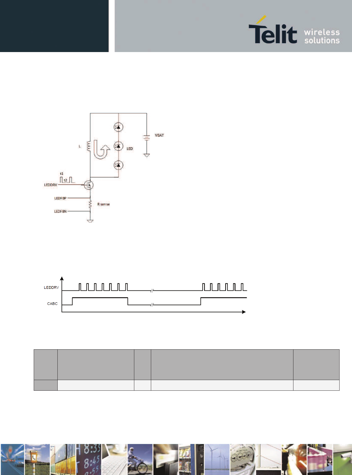
xE922-3GR Hardware User Guide
1VV0301272 Rev.0.8 2017-01-05
Reproduction forbidden without written authorization from Telit Communications S.p.A. - All Rights
Reserved. Page 65 of 112
A typical application of the backlight control is drawn in below figure .
LEDDRV controls the gate of an external NFET with PWM signal.
During first time period t1 the inductor L is charged via the n-channel FET closed , while during second period
t2 the inductor L is discharged via the parallel LED’s.
CABC = Content Adaptive Backlight Control input from external backlighting control IC.
In order to keep the ‘perceived’ brightness the same, the brightness of the LED backlight can be dimmed while
increasing the light shining through the LCD filter. When CABC operation is enabled, the LEDDRV PWM is
kept low/disabled when the CABC signal is low.
This way the backlight power consumption can be reduced.
Please consult the appropriate application note on Intel’s IBL support website.
10.4. LED_CURSINK
PAD
Signal
I/O
descriptions Type
AR14
LED_CURSINK
I
GP LED Driver (Sink)
Analog
The LED_CURSINK features a programmable (in steps of 2mA) current sink up to 40mA, typically used for
LED keypad backlighting.
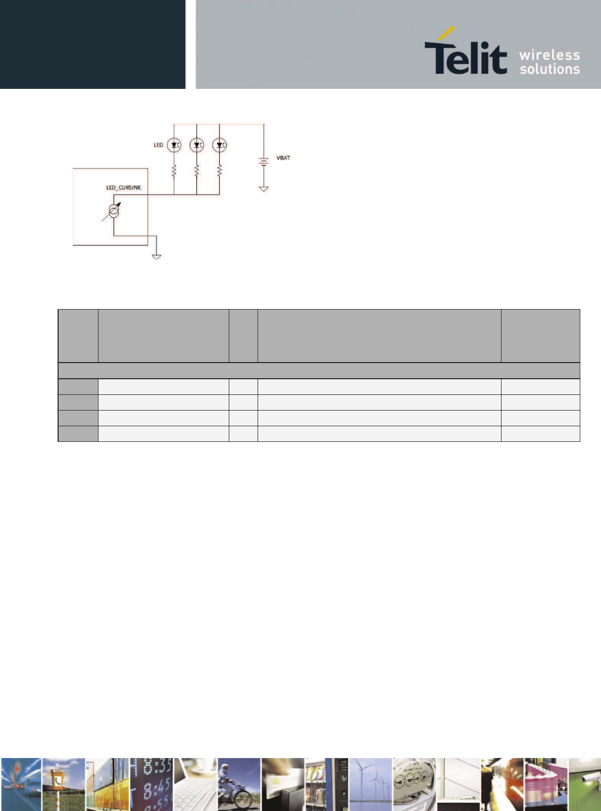
xE922-3GR Hardware User Guide
1VV0301272 Rev.0.8 2017-01-05
Reproduction forbidden without written authorization from Telit Communications S.p.A. - All Rights
Reserved. Page 66 of 112
10.5. Touch panel
PAD
Signal
I/O
descriptions Type
Touch Screen interface
AD17
TP_SDA
I/O
Touch panel I2C Data
CMOS 1.8V
AB17
TP_SCL
I/O
Touch panel I2C Clock
CMOS 1.8V
F7
TP_RESET
I/O
Touch panel Reset
CMOS 1.8V
F11
TP_IRQ
I/O
Touch panel Interrupt
CMOS 1.8V
A dedicated I2C bus and control lines are foreseen to interface with an external touch panel control IC.
Besides touch panel interface, this I2C bus can also be applied for display EDID retrieval at boot time.
In case touch panel is not used, the above signals can be used as GPIO’s, interrupts or general purpose I2C.
xE922-3GR Hardware User Guide
1VV0301272 Rev.0.8 2017-01-05
Reproduction forbidden without written authorization from Telit Communications S.p.A. - All Rights
Reserved. Page 67 of 112
11. Camera interface
The xE922-3GR module offers two CIF camera interfaces.
MIPI CSI-2 compliant, utilizing MIPI DPHY as physical layer.
Max rate of bit clock of a DPHY lane is defined as 500MHz, or equivalent datarate 1Gbps.
Atom x3 chipset ISP throughput limited to max 221Mpix/sec
Please consult Intel’s IBL Support website for AVL (approved vendor list), as well for recommended
implementation and port assignment
PAD
Signal
I/O
descriptions Type
Main Camera
D21
CSI1_DP0
AI
Main Camera CSI Data0 Input Positive
Analog
F21
CSI1_DN0
AI
Main Camera CSI Data0 Input Negative
Analog
M19
CSI1_DP1
AI
Main Camera CSI Data1 Input Positive
Analog
K19
CSI1_DN1
AI
Main Camera CSI Data1 Input Negative
Analog
F19
CSI1_DP2
AI
Main Camera CSI Data2 Input Positive
Analog
H19
CSI1_DN2
AI
Main Camera CSI Data2 Input Negative
Analog
E18
CSI1_DP3
AI
Main Camera CSI Data3 Input Positive
Analog
G18
CSI1_DN3
AI
Main Camera CSI Data3 Input Negative
Analog
C20
CSI1_CLKP
AI
Main Camera CSI Clock Positive
Analog
E20
CSI1_CLKN
AI
Main Camera CSI Clock Negative
Analog
P17
CAM_MCLK
O
Camera MCLK output
CMOS 1.8V
AM17
CAM_I2C_SDA
I/O
Camera I2C Data
CMOS 1.8V
AP17
CAM_I2C_SCL
I/O
Camera I2C Clock
CMOS 1.8V
A4
CAM1_PD
I/O
Main Camera Power Down / GPIO
CMOS 1.8V
G4
CAM1_RESET
I/O
Main Camera Reset / GPIO
CMOS 1.8V
B7
CAM1_FLASH
I/O
Main Camera Flash Triger
CMOS 1.8V
G6
CAM1_TORCH
I/O
Main Camera Torch Enable
CMOS 1.8V
Secondary Camera
A18
CSI2_DP
AI
Sub Camera CSI Data Input Positive
Analog
C18
CSI2_DN
AI
Sub Camera CSI Data Input Negative
Analog
B19
CSI2_CLKP
AI
Sub Camera CSI Clock Positive
Analog
D19
CSI2_CLKN
AI
Sub Camera CSI Clock Negative
Analog
H3
CAM2_PD
I/O
Sub Camera Power Down / GPIO
CMOS 1.8V
E4
CAM2_RESET
I/O
Sub Camera Reset / GPIO
CMOS 1.8V
Camera power supply
AA18
VAUX_1P8V
-
Camera/Auxiliary 1.8V power supply
POWER
AH17
VAUX_2P85V
-
Camera/Auxiliary power supply 1 (2.85V)
POWER
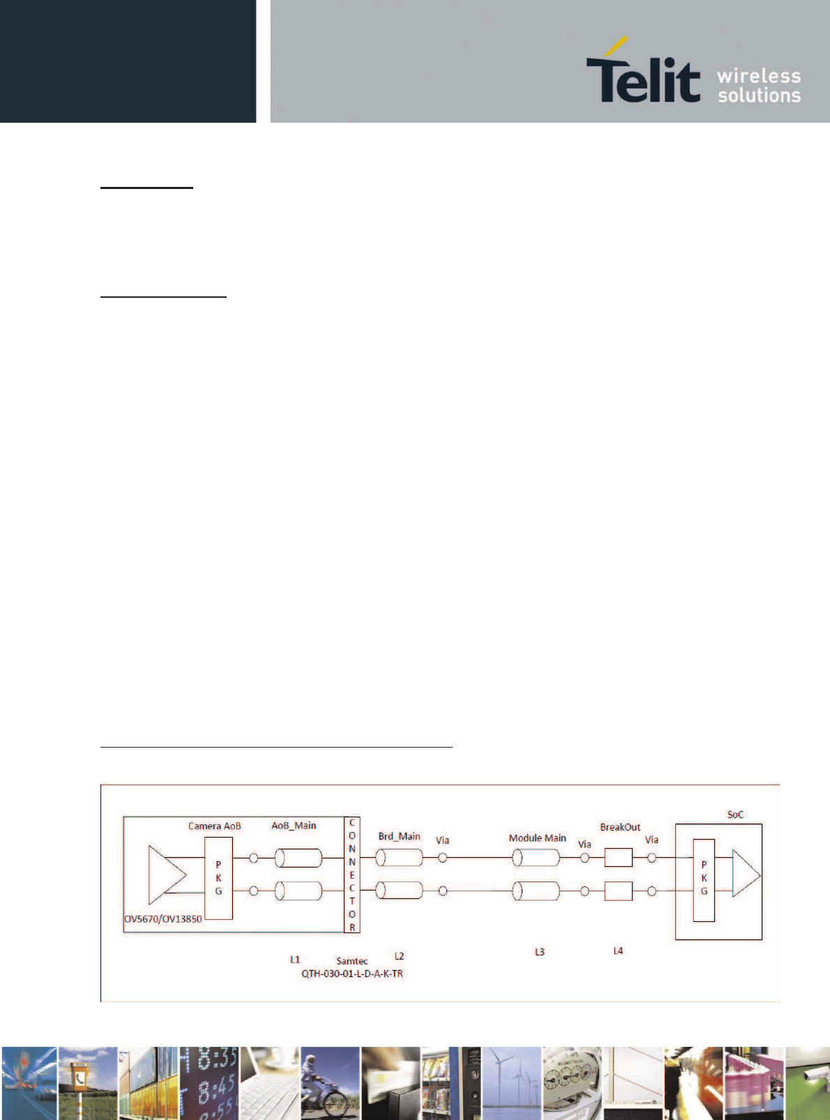
xE922-3GR Hardware User Guide
1VV0301272 Rev.0.8 2017-01-05
Reproduction forbidden without written authorization from Telit Communications S.p.A. - All Rights
Reserved. Page 68 of 112
Main camera:
· High resolution up to 13Mpixel /15 fps
· 4-lane MIPI CSI-2
· up to 550Mbps/lane data rate ( limited by ISP throughput)
Secondary camera:
· Low resolution up to 5Mpixel
· 1-lane MIPI CSI-2
· up to 1Gbps/lane data rate
The cameras cannot be used simultaneously, only 1 at the time.
A dedicated CAM_I2C bus interfaces is featured to control the CMOS camera devices (external pullup
resistors to VAUX_1P8V required), as well as CAM_RESET and CAM_PD control pins for each CIF
interface.
The reference clock CAM_MCLK frequency is max 26MHz.
CAM1_FLASH and _TORCH enable flash and torch resp. of main camera.
In case the Camera interface is not used, the above signals can be used as GPIO’s, interrupts or general
purpose I2C (in that case add external pullup resistors to 1V8_OUT)
Two voltage regulators can be used for camera device supply:
· VAUX_1P8V
· VAUX_2P85V
Both have a current rating of max 225mA.
Typically 1uF external decoupling capacitance to be added (additional to internal 1uF).
In case not applied for camera supply, both regulators can be used for other purpose.
Routing guide lines for the display MIPI-CSI-2 interface:
The next figure shows a typical signal traject with different sub trajects.
xE922-3GR Hardware User Guide
1VV0301272 Rev.0.8 2017-01-05
Reproduction forbidden without written authorization from Telit Communications S.p.A. - All Rights
Reserved. Page 69 of 112
Recommended routing guidelines for the whole MIPI-CSI-2 signal traject :
parameter
guideline
Characteristic
impedance (stripline / microstrip)
100 ohm differential 10%(SL) 15%(MS)
Trace spacing : between differential pairs or between
differential pair and other signals (h = dielectric height)
5xh (SL) 7xh (MS)
Total length
(add
-on pcb (L1)+ carrier (L2)+ (module (L3+L4))
Min. 45.7 mm / Max. 203.2 mm (MS/SL)
Max. n
umber of vias allowed
2 through
-
hole vias + 3 microvias + 2
connector pins
Length matching between P and N within a differential pair
Within same layer mismatch: +/
-
0.254 mm
Total length mismat
ch: +/-0.381 mm
Length matching between DATA to CLK
Within same layer mismatch : +/
-
1.27 mm
Total length mismatch: +/
- 2.54 mm
Guidelines for off-module sub trajects:
parameter
Addon board
Carrier board
Transmission line segment
L1
L2
Length [mm]
12.7
– 63.5 (MS)
12.7
– 88.9 (MS/SL)
Actual xE922-3GR module signal trace (L3+L4) implementation:
signal name
module
trace length
[mm]
Number of microvias
on the module
CSI1_CLKN
9.99
2
CSI1_CLKP
9.79
2
CSI1_DN0
10.97
2
CSI1_DP0
11.22
2
CSI1_DN1
7.26
2

xE922-3GR Hardware User Guide
1VV0301272 Rev.0.8 2017-01-05
Reproduction forbidden without written authorization from Telit Communications S.p.A. - All Rights
Reserved. Page 70 of 112
CSI1_DP1
7.48
2
CSI1_DN2
7.77
2
CSI1_DP2
7.52
2
CSI1_DN3
7.31
2
CSI1_DP3
7.26
2
signal name
module
trace length
[mm]
Number of microvias
on the module
CSI2_CLKN
10.04
2
CSI2_CLKP
10.26
2
CSI2_DN
10.46
2
CSI2_DP
10.7
2
xE922-3GR Hardware User Guide
1VV0301272 Rev.0.8 2017-01-05
Reproduction forbidden without written authorization from Telit Communications S.p.A. - All Rights
Reserved. Page 71 of 112
12. Peripheral interfaces
12.1. I2C
The xE922-3GR offers in total four I2C bus interfaces.
1V8 IO, standard/fast mode SCLK 100 kHz/400 kHz.
The below table gives an overview and indicates the assigned functions that are ‘reserved’ for each I2C bus
port.
PAD
Signal
I/O
descriptions Type
AM17
CAM_I2C_SDA
I/O
Camera I2C Data
CMOS 1.8V
AP17
CAM_I2C_SCL
I/O
Camera I2C Clock
CMOS 1.8V
AD17
TP_SDA
I/O
Touch panel I2C Data
CMOS 1.8V
AB17
TP_SCL
I/O
Touch panel I2C Clock
CMOS 1.8V
AC18
CHG_I2C_SCL
I/O
Charger I2C Clock
CMOS 1.8V
AE18
CHG_I2C_SDA
I/O
Charger I2C Data
CMOS 1.8V
AS1
AUX_I2C_SDA
I/O
I2C3 Data (AUX / Sensors)
CMOS 1.8V
AT2
AUX_I2C_SCL
I/O
I2C3 Clock (AUX / Sensors)
CMOS 1.8V
· CAM_I2C signal lines need external 2.2k pullup resistors to VAUX_1P8V.
· TP_/CHG_/AUX_ I2C signal lines have internal 2.2k pullup resistors to 1V8_OUT
Care should be taken to limit the total bus load capacitance to meet maximum rise time requirement of 300ns
(fast-mode) or 1 µs (standard-mode).
None of these I2C bus ports are connected internal the module to other peripherals.
In case not applied for the reserved functions, the camera and touch panel I2C busses can be applied for
general use case. In that case CAM_I2C signal lines should be pulled up to 1V8_OUT.
The charger I2C interface is dedicated and cannot be used for other purpose
xE922-3GR Hardware User Guide
1VV0301272 Rev.0.8 2017-01-05
Reproduction forbidden without written authorization from Telit Communications S.p.A. - All Rights
Reserved. Page 72 of 112
12.2. USIF
xE922-3GR offers two ‘Universal Serial Interface’ ports, configurable either as SPI or UART
· USIF1 :SPI (up to 48MHz) / UART
· USIF2 :SPI (up to 26MHz) / UART
PAD
Signal
I/O
descriptions Type
USIF 1 (UART/SPI)
W5
USIF1_RXD
I
UART1 / SPI1 Serial data input
CMOS 1.8V
Y5
USIF1_TXD
O
UART1 / SPI1 Serial data Output
CMOS 1.8V
S5
USIF1_SCLK
I/O
UART1 RTS / SPI1 SCLK
CMOS 1.8V
U5
USIF1_CS
O
UART1 CTS / SPI1 Chip Select
CMOS 1.8V
USIF 2 (UART/SPI)
AH3
USIF2_RXD
I
UART2 / SPI2 Serial data input
CMOS 1.8V
AE4
USIF2_TXD
O
UART2 / SPI2 Serial data Output
CMOS 1.8V
AD5
USIF2_SCLK
I/O
UART2 CTS / SPI2 SCLK
CMOS 1.8V
AJ2
USIF2_CS
O
UART2 RTS / SPI2 Chip Select
CMOS 1.8V
Remark:
USIF1 pinning is also multiplexed with an optional digital audio I2S interface bus (refer to audio chapter).
Routing guide lines for the USIF interface (SPI mode):
Recommended routing guidelines for the whole USIF signal traject:
parameter
guideline
Characteristic impedance (stripline / microstrip)
50 ohm single ended 10%(SL) 15%(MS)
Trace spacing : between differential pairs or between
differential pair and other signals (h = dielectric height)
2xh (SL) 3xh (MS)
Total length
(module (L1) + carrier(L2))
Min. 5.1 mm / Max. 330.2 mm (MS/SL)
Max. number of vias allowed
4 through
-hole vias + 4 microvias
Length matching between DATA to CLK
Total length mismatch: +/
- 12.7 mm
xE922-3GR Hardware User Guide
1VV0301272 Rev.0.8 2017-01-05
Reproduction forbidden without written authorization from Telit Communications S.p.A. - All Rights
Reserved. Page 73 of 112
Actual xE922-3GR module signal trace (L1) implementation USIF1:
signal name
module
trace length
[mm]
Number of microvias on
the module
USIF1_SCLK
24.8
3
USIF1_RXD
20.8
3
USIF1_TXD
20.2
3
USIF1_CS
22.2
3
Actual xE922-3GR module signal trace (L1) implementation USIF2:
signal name
module
trace length
[mm]
Number of microvias on
the module
USIF
2_SCLK
60.8
3
USIF
2_RXD
59.2
3
USIF
2_TXD
59.4
3
USIF
2_CS
58.7
3
xE922-3GR Hardware User Guide
1VV0301272 Rev.0.8 2017-01-05
Reproduction forbidden without written authorization from Telit Communications S.p.A. - All Rights
Reserved. Page 74 of 112
12.3. SDMMC/SDIO
SDIO: SD 3.0, 1x 4bit, speed up to DDR50 (clk 48MHz) / SDR50 (clk 96MHz), only 1.8V supported
SDMMC: SD 3.0, 1x 4bit, default mode 26MHz, including power supply VDD_SD (fixed to 2.9V) and card
detect
Note:
In case SDMMC 1.8V support is needed, an external 3.0V voltage regulator should be added (ENABLE pin
controlled by VDD_SD line), to supply card VDD pin of the card holder.
PAD
Signal
I/O
descriptions Type
SD/MMC Card Interface
AP15
VDD_SD
-
Power supply out for SDMMC card
2.9V
J2
SD_CARD_DET
I
MMC card detect(active low)
CMOS_1.8V
F1
SD_DAT0
I/O
MMC card data 0
CMOS_1.8/3V
H1
SD_DAT1
I/O
MMC card data 1
CMOS_1.8/3V
K1
SD_DAT2
I/O
MMC card data 2
CMOS_1.8/3V
M1
SD_DAT3
O
MMC card data3
CMOS_1.8/3V
E2
SD_CLK
O
MMC card clock
CMOS_1.8/3V
G2
SD_CMD
I/O
MMC card command
CMOS_1.8/3V
SDIO Interface
L4
SDIO_CLK
I/O
CLK
CMOS 1.8V
P3
SDIO_CMD
I/O
CMD
CMOS 1.8V
P1
SDIO_DAT0
I/O
SD0
CMOS 1.8V
N2
SDIO_DAT1
I/O
SD1
CMOS 1.8V
M3
SDIO_DAT2
I/O
SD2
CMOS 1.8V
N4
SDIO_DAT3
I/O
SD3
CMOS 1.8V
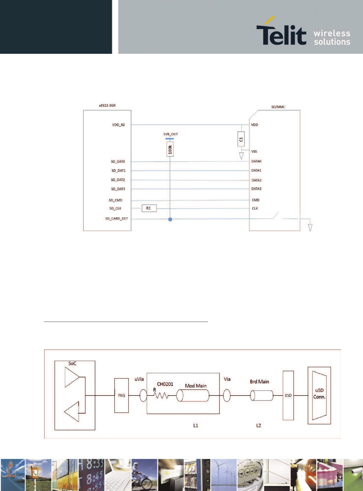
xE922-3GR Hardware User Guide
1VV0301272 Rev.0.8 2017-01-05
Reproduction forbidden without written authorization from Telit Communications S.p.A. - All Rights
Reserved. Page 75 of 112
A typical diagram for SDMMC card connection is shown in below figure.
Series resistor R1 place holder is recommended for tuning high speed CLK signal, typ.27 Ohm.
Internal regulator VDD_SD supports dual voltage level 2.9V (default)/1.8V, with current rating max 255 mA.
Maximum decoupling capacitance C1 is up to 5 uF (including the internal 1uF decoupling already present).
In case ESD protection to be applied, use high speed device < 2pF.
Routing guide lines for the display SDMMC/SDIO interface:
The next figure shows a typical signal traject with different sub trajects.
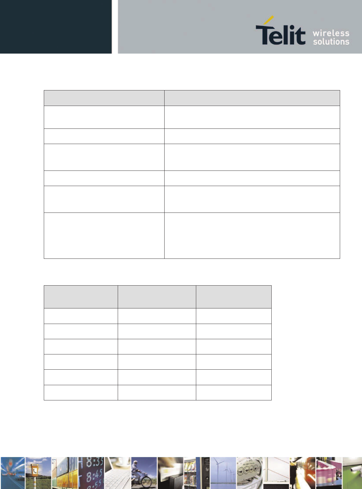
xE922-3GR Hardware User Guide
1VV0301272 Rev.0.8 2017-01-05
Reproduction forbidden without written authorization from Telit Communications S.p.A. - All Rights
Reserved. Page 76 of 112
Recommended routing guidelines for the whole SDMMC/SDIO signal traject:
parameter
guideline
Characteristic impedance (stripline /
microstrip)
50 ohm single ended 10%(SL) 15%(MS)
Trace spacing (h = dielectric height)
2
xh (SL) 3xh (MS)
Total length
(module (L1) +
carrier(L2))
Min.
12.7 mm / Max. 88.9 mm (MS/SL)
Max. n
umber of vias allowed
4 through
-hole vias + 3 microvias
Length matching between DATA/CMD to
CLK
Within same layer mismatch : +/
- 1.27 mm
Total length mismatch: +/
- 2.54 mm
Termination resistors
(Note: no series resistors implemented on
xE922
-3GR module side )
Rseries on CLK is 27 ohm +/
-
10%, and on DAT 39 ohm +/-
10%. The series resistor placeholder should be close to module
CLK, DATA and CMD lanes. Use of the resistor is to improve
signal quality
.Based on validation data, resistor can be
removed
or retained on the board
Actual xE922-3GR module signal trace (L1) implementation:
signal name
module
trace length
[mm]
Number of microvias on
the module
SDIO_CLK
18.81
3
SDIO_CMD
18.4
0
5
SDIO_DAT0
19.85
3
SDIO_DAT1
18.39
4
SDIO_DAT2
17.65
4
SDIO_DAT3
17.62
4
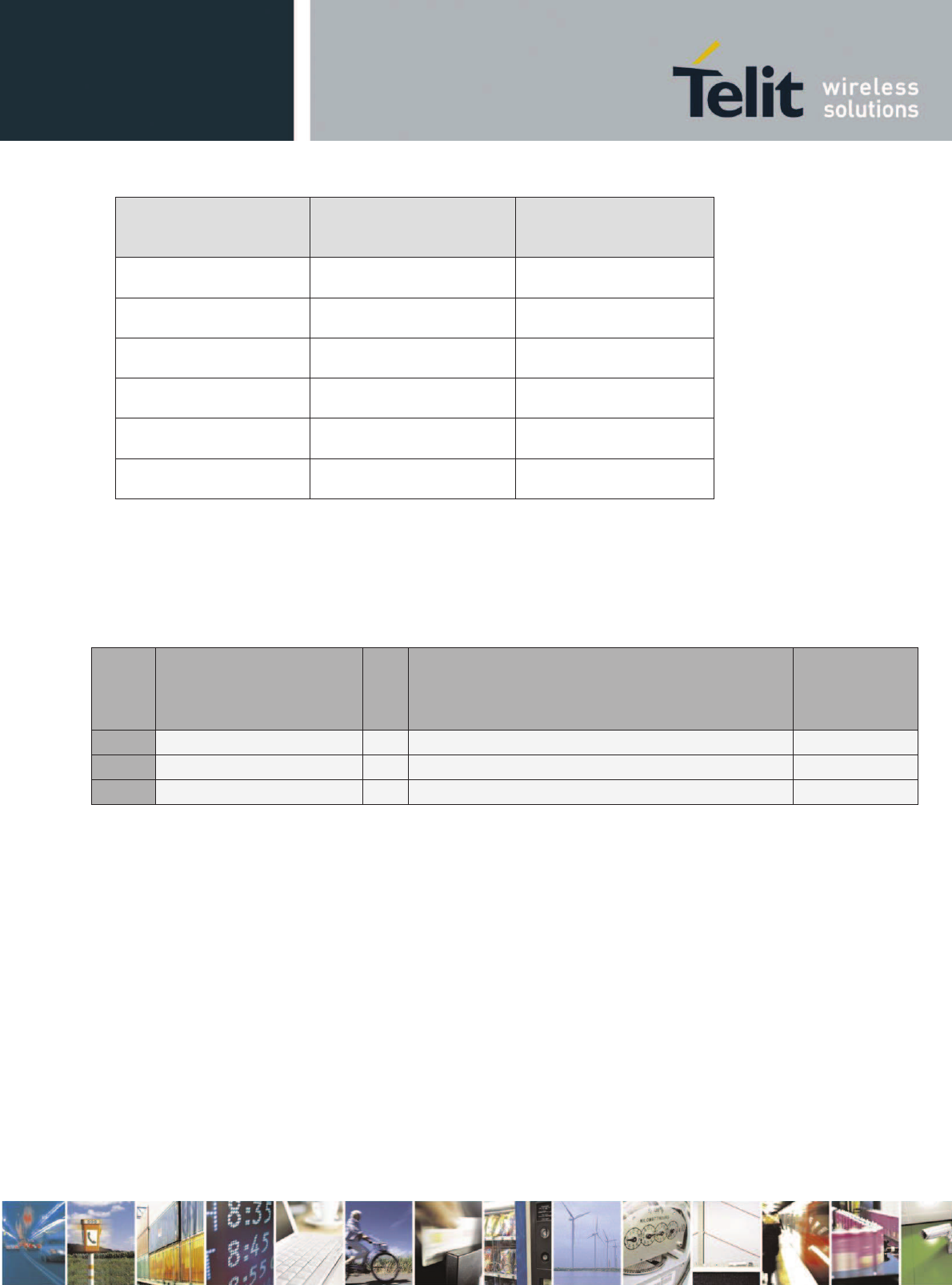
xE922-3GR Hardware User Guide
1VV0301272 Rev.0.8 2017-01-05
Reproduction forbidden without written authorization from Telit Communications S.p.A. - All Rights
Reserved. Page 77 of 112
signal name
module
trace length
[mm]
Number of microvias on
the module
SD_CLK
37.86
4
SD_CMD
37.26
4
SD_DAT0
37.79
4
SD_DAT1
36.54
4
SD_DAT2
35.72
4
SD_DAT3
36.49
4
12.4. ADC
xE922-3GR offers in total three ADC input lines:
PAD
Signal
I/O
descriptions Type
AM19
ADC_VBATMEAS
I
Battery measurement ADC
Analog
AL18
ADC_IN0
AI
Analog to Digital converter 1 (Batt ID)
Analog
AK19
ADC_IN1
AI
Analog to Digital converter 2 (Batt Temp)
Analog
When the system implements an external battery charger IC circuitry, the above pin description explains the
reserved usage in that case. When no charger IC is implemented, ADC_IN0 and _IN1 can be used for general
purpose ADC input.
ADC_VBATMEAS still needs to be applied at the main supply pin V_BAT of the module in order to properly
boot the system.
ADC_INx properties:
· resolution : 12 bit
· input voltage range : 0V … 1.2V (for ADC_IN0/1)
· input resistance: minimum 1 MOhm
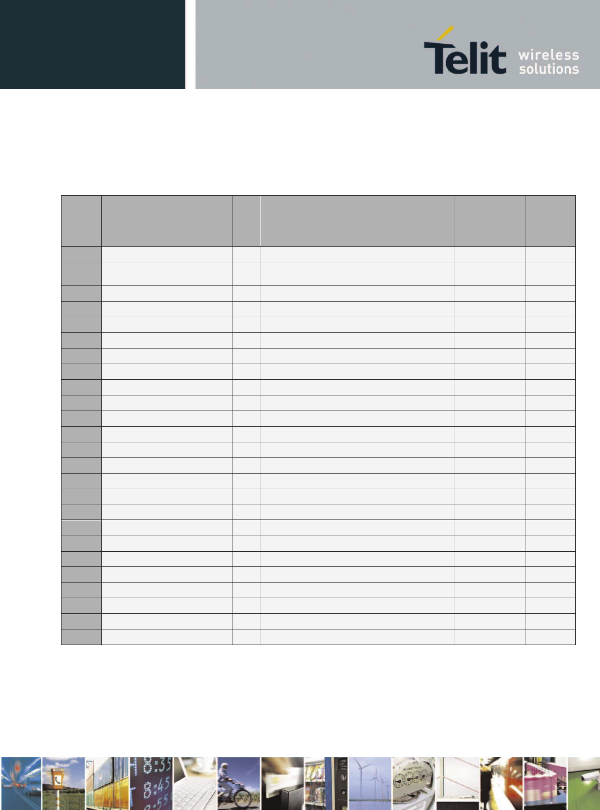
xE922-3GR Hardware User Guide
1VV0301272 Rev.0.8 2017-01-05
Reproduction forbidden without written authorization from Telit Communications S.p.A. - All Rights
Reserved. Page 78 of 112
13. General purpose I/O
The following table gives an overview of the xE922-3GR pins that are ‘suggested’ for general purpose I/O use
case:
PAD
Signal
I/O
descriptions Type
Reset
state
AV8
GPIO0_EINT5
I/O
GPIO / External IRQ
CMOS 1.8V
T/PD
AT8
GPIO1_EINT2
I/O
GPIO / External IRQ, Used for SoC USB ID
WU from Sleep
CMOS 1.8V
T/PD
AS11
GPIO5_EINT7
I/O
GPIO / USB_FAULT IRQ
CMOS 1.8V
T/PD
G10
GPIO44
I/O
GPIO
CMOS 1.8V
T/PD
E10
GPIO45
I/O
GPIO
CMOS 1.8V
T/PD
A10
GPIO46
I/O
GPIO
CMOS 1.8V
T/PD
H9
GPIO47
I/O
GPIO
CMOS 1.8V
T/PD
F9
GPIO48
I/O
GPIO
CMOS 1.8V
T/PD
B9
GPIO49
I/O
GPIO
CMOS 1.8V
T/PD
G8
GPIO50
I/O
GPIO
CMOS 1.8V
T/PD
E8
GPIO51
I/O
GPIO
CMOS 1.8V
T/PD
A8
GPIO52_EINT15
I/O
GPIO / External IRQ
CMOS 1.8V
T/PD
H17
GPIO53
I/O
GPIO / MIPI Trace Clock
CMOS 1.8V
T/PD
K5
GPIO54_EINT1
I/O
GPIO / External IRQ
CMOS 1.8V
T/PD
G14
GPIO55_EINT15
I/O
GPIO / External IRQ
CMOS 1.8V
T/PD
H7
GPIO56
I/O
GPIO
CMOS 1.8V
T/PD
B11
GPIO57_EINT9
I/O
GPIO / External IRQ
CMOS 1.8V
T/PD
D11
GPIO58_EINT2
I/O
GPIO / External IRQ
CMOS 1.8V
T/PD
E6
GPIO63_EINT8
I/O
GPIO / External IRQ
CMOS 1.8V
T/PD
A6
GPIO64_EINT13
I/O
GPIO / External IRQ
CMOS 1.8V
T/PD
H5
GPIO65
I/O
GPIO
CMOS 1.8V
T/PD
F5
GPIO66_EINT15
I/O
GPIO / External IRQ
CMOS 1.8V
T/PD
B5
GPIO67_EINT0
I/O
GPIO / External IRQ
CMOS 1.8V
T/PD
F3
GPIO72_EINT9
I/O
GPIO / External IRQ
CMOS 1.8V
T/PD
B3
GPIO73_EINT10
I/O
GPIO / External IRQ
CMOS 1.8V
T/PD
As indicated in the table some of these GPIO’s can be configured for external interrupt /wake up (edge, level
detect). The optional GPIO’s defined for camera or display control, in case not applied, can also be applied for
general use case.

xE922-3GR Hardware User Guide
1VV0301272 Rev.0.8 2017-01-05
Reproduction forbidden without written authorization from Telit Communications S.p.A. - All Rights
Reserved. Page 79 of 112
Each SoC pad’s characteristics are controlled by a peripheral called PCL (Port Control Logic).
In the next page table a ‘complete’ overview of all PCL muxing options for ‘all DBB pins externally
available’ on the xE922-3GR module LGA pinout is detailed out.
In order to clarify the correspondence between the module’s pin naming and chip set supplier documentation
naming convention, the DBB SoC BGA ball pin /signal names as well as xE922-3GR LGA pin number /
signal names are indicated in different columns.
Yellow color code highlights the xE922-3GR module’s intentional target use.
Note:
Please note GPIO2_EINT4 is applicable as “input only” because of internal level shift circuitry to
accommodate for 5V VBUS_USB level detect.
Please consult Intel Business Link Support (IBL) for detailed info (like SW user guide) how to program the
GPIO configuration/multiplex for your specific application.
Each pad has following characteristics indicated:
Pad pull class: This is the pull-up and pull-down strength of the pad that can be enabled/disabled using PCL
registers. There are three pull classes of pads on 1.8V IO domain, A, B, and D (C is not used). A is the
strongest (PU=155uA typ, PD=135uA Typ), B is medium (PU=80.8uA typ, PD=64uA typ) and D is the
weakest (PU=16.4uA typ, PD=16.2uA typ). Pull-up/pull-down can be enabled through PCL registers but their
strength is fixed as indicated in the GPIO spreadsheet, refer to it for each individual pad’s pull class.
Drive strength, also referred to as drive/output current for the pad. 2mA, 4mA, 8mA and 12mA are supported
and can be selected by PCL register.
Buffer Type: Schmitt Trigger ST or buffer BU. This setting is not selectable through PCL registers. Refer to
GPIO spreadsheet for each individual pad’s buffer type.
RESET state during RESET (PU or PD): All pads come up in a default state during and after reset until
PCL registers are initialized. It is important to note that connection of each GPIO to application circuit
requires determination whether application circuit is sensitive to the GPIO being HIGH or LOW at reset, e.g.,
it might not be desirable to have an RF transmitter enabled by default during power-on reset so the GPIO
allocated to its RESET and/or power-down input should be such that it holds the transmitter in “disabled”
state at the time of power-on until SW takes control. Refer to GPIO table for each individual pad’s default
state at reset.
Signal direction during RESET (input or output): Refer to GPIO table for each individual pad’s default
direction at reset.
Functions multiplexed on each pad: Each pad not associated with dedicated interfaces can have up to 7
alternate functions multiplexed on it in addition to GPIO function. Refer to GPIO table for each individual
pad’s alternate functions.
Interrupts: the chip set supports sixteen external interrupts (EINT[15:0]) signals that are multiplexed on
different pins but can only be used in one location. Not all interrupt signals are available as some are on pins
used for dedicated functions.
GPIOs and their different aspects described above can be configured through SW. Please refer to software
architecture document for more details.
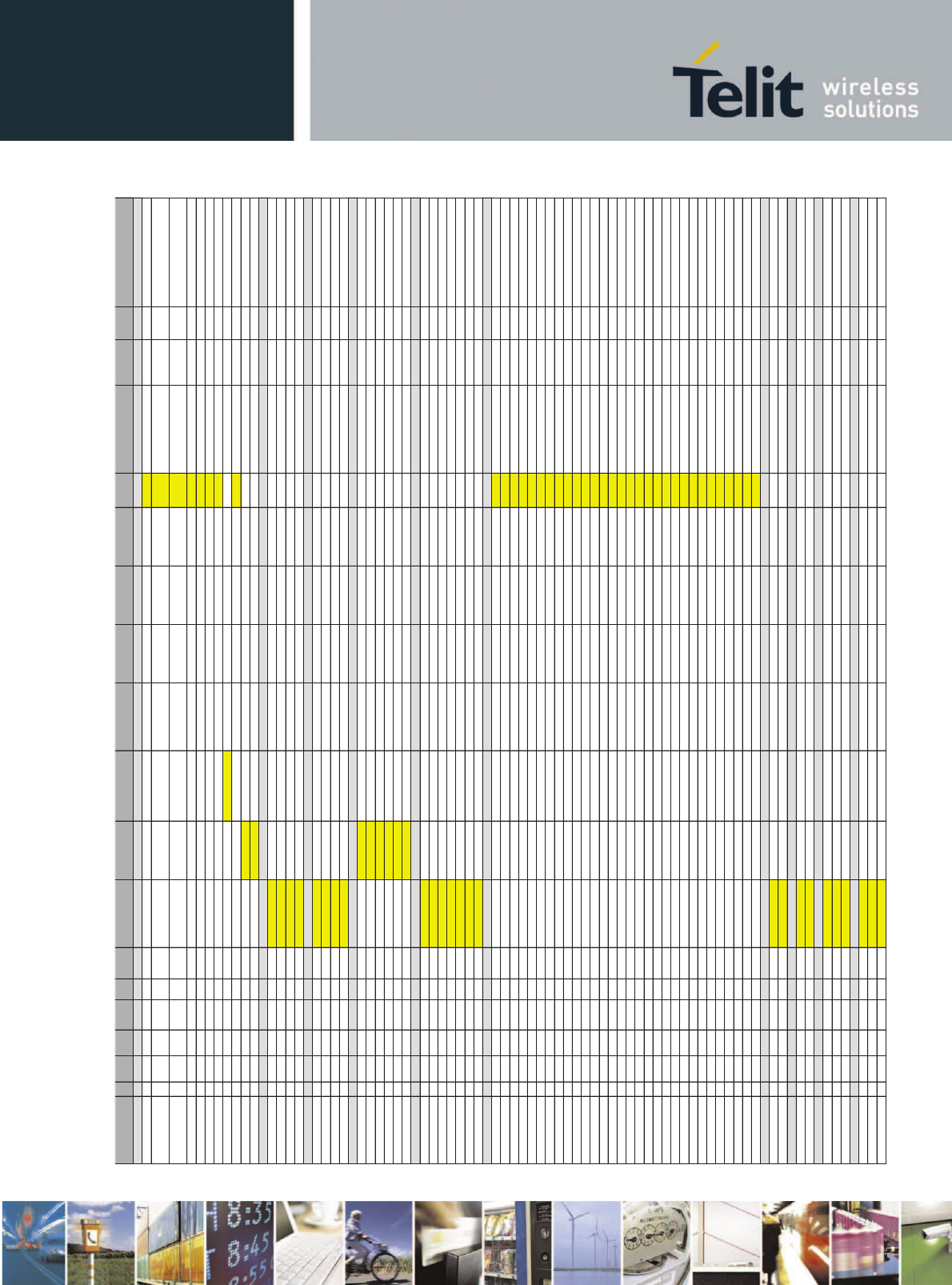
xE922-3GR Hardware User Guide
1VV0301272 Rev.0.8 2017-01-05
Reproduction forbidden without written authorization from Telit Communications S.p.A. - All Rights
Reserved. Page 80 of 112
SoC Pin Name
SoC
Ball
I/O
@ Reset
State
@ Reset
voltage
domain
buffer
type
DBB
pull class
F1 F2 F3 F4 F5 F6 F7 GPIO Index xE922_3GR Selected Function
xE9223GR
Signal Name
xE922_3GR
LGA PIN#
Description
#DBB KEYPAD I/F
KP_IN0
C20 I T/PD 1.8V ST A KP_IN0 MIPI_TRACE_DATA0 0 MIPI_TRACE_DATA8 TRACE_CADATA HW_MON4 EINT_5 GPIO_000 EINT_5 GPIO0_EINT5 AV8 GPIO / External IRQ
KP_IN1
D20 I T/PD 1.8V ST A KP_IN1 MIPI_TRACE_DATA1 PWM1 MIPI_TRACE_DATA9 TRACE_CAFLAG HW_MON5 EINT_2 GPIO_001 EINT_2 GPIO1_EINT2 AT8
External IRQ,
Used for SoC USB ID WU from Sleep
KP_IN2
C21 I T/PD 1.8V ST A KP_IN2 MIPI_TRACE_DATA2 0 MIPI_TRACE_DATA10 TRACE_CAREADY HW_MON6 EINT_4 GPIO_002 EINT_4 VBUS_DET AR8
External IRQ,
used for VBUS Detection
KP_OUT0 D21 I T/PD 1.8V ST A KP_OUT0 MIPI_TRACE_DATA3 CC2_IN MIPI_TRACE_DATA11 TRACE_ACDATA HW_MON7 EINT_6 GPIO_003 CC2_IN USIM2_DETECT AR10 USIM2_Detect
KP_OUT1 E17 I T/PD 1.8V ST A KP_OUT1 MIPI_TRACE_CLK CC1_IN 0 TRACE_ACFLAG HW_MON8 ETM7_PIPESTAT0 GPIO_004 CC1_IN USIM1_DETECT AN10 USIM1_Detect
KP_OUT2 C19 I T/PD 1.8V ST A KP_OUT2 MIPI_TRACE_DATA4 DSP_2G_IN0 MIPI_TRACE_DATA12 TRACE_ACREADY HW_MON9 EINT_7 GPIO_005 EINT_7 GPIO5_EINT7 AS11 GPIO / USB_FAULT IRQ
KP_OUT3 D19 I T/PD 1.8V ST A KP_OUT3 MIPI_TRACE_DATA5 DSP_2G_IN1 MIPI_TRACE_DATA13 GPO_3G_0 HW_MON10 ETM7_PIPESTAT1 GPIO_006 GPIO_006 LCD_RESET AP11 LCD Reset
KP_IN3 E20 I T/PD 1.8V ST A KP_IN3 MIPI_TRACE_DATA6 POS_FTA_FTR MIPI_TRACE_DATA14 GPO_3G_1 HW_MON11 ETM7_PIPESTAT2 GPIO_007 GPIO_007 GPIO7 AN8 GNSS_FTA
KP_IN5 C18 I T/PD 1.8V ST A KP_IN5 CC0_CC0IO DSP_2G_OUT0 CC1_CC1IO GPO_3G_3 HW_MON13 EINT_3 GPIO_009 EINT_3 LCD_TE AP9 LCD Tearing effect input
KP_IN6 B20 I T/PD 1.8V ST A KP_IN6 I2C3_SDA POS_FTA_FTR CC0_CC2IO DSP_AUDIO_OUT0 HW_MON14 0 GPIO_010 I2C3_SDA AUX_I2C_SDA AS1 I2C3 Data (AUX / Sensors)
KP_OUT4 D17 I T/PD 1.8V ST A KP_OUT4 I2C3_SCL EINT_4 CC0_CC5IO DSP_AUDIO_OUT1 HW_MON15 CLKOUT0 GPIO_011 I2C3_SCL AUX_I2C_SCL AT2 I2C3 Clock (AUX / Sensors)
#DBB USIF1
USIF1_RXD_MRST G3 I T/PD 1.8V ST A USIF1_RXD_MRST 0 EINT_0 I2S1_RX DSP_AUDIO_OUT2 HW_MON16 PWM0 GPIO_012 USIF1_RXD_MRST USIF1_RXD W5 UART1 / SPI1 Serial data input
USIF1_TXD_MTSR G2 I T/PD 1.8V ST A USIF1_TXD_MTSR 0 KP_OUT5 I2S1_TX EINT_1 0 0 GPIO_013 USIF1_TXD_MTSR USIF1_TXD Y5 UART1 / SPI1 Serial data Output
USIF1_CSO0 G5 I T/PD 1.8V ST A USIF1_CSO0 0 KP_OUT6 I2S1_WA0 EINT_3 USIF1_CTS_N CC1_IN GPIO_014 USIF1_CSO0 USIF1_SCLK S5 UART1 CTS / SPI1 SCLK
USIF1_SCLK G4 I T/PD 1.8V ST A USIF1_SCLK 0 KP_OUT7 I2S1_CLK0 CC2_IN USIF1_RTS_N EINT_9 GPIO_015 USIF1_SCLK USIF1_CS U5 UART1 RTS / SPI1 Chip Select
#DBB USIF2
USIF2_RXD_MRST E12 I T/PD 1.8V ST A USIF2_RXD_MRST 0 EINT_10 EINT_6 CC0_CC4IO 0 CIF_PRELIGHT_TRIG GPIO_016 USIF2_RXD_MRST USIF2_RXD AH3 UART2 / SPI2 Serial data input
USIF2_TXD_MTSR E10 I T/PD 1.8V ST A USIF2_TXD_MTSR 0 CC1_CC0IO EINT_11 USI_T_IN_TIME_EXT POS_FTA_FTR CIF_FL_TRIG_OUT GPIO_017 USIF2_TXD_MTSR USIF2_TXD AE4 UART2 / SPI2 Serial data Output
USIF2_RTS_N A12 I T/PD 1.8V ST A USIF2_RTS_N 0 EINT_12 USIF2_CSO0 KP_IN7 USIF2_CSI_N CIF_SHUTTER_TRIG GPIO_018 USIF2_RTS_N USIF2_SCLK AD5 UART2 CTS / SPI2 SCLK
USIF2_CTS_N A13 I T/PD 1.8V ST A USIF2_CTS_N 0 BREAK_IN USIF2_SCLK CC1_IN EINT_13 CIF_SHUTTER_OPEN GPIO_019 USIF2_CTS_N USIF2_CS AJ2 UART2 RTS / SPI2 Chip Select
#DBB NAND
NAND_ALE U6 O L 1.8V ST A NAND_ALE SDIO_CMD USIRFSEQGP0_3G KP_IN6 EINT_10 RTCK CC1_CC4IO GPIO_031 SDIO_CMD SDIO_CMD P3 WLAN SDIO Command
NAND_RDN V5 O H 1.8V ST A NAND_RDN SDIO_DAT0 USIRFSEQGP1_3G KP_OUT4 EINT_11 CC1_CC3IO USIF2_RTS_N GPIO_032 SDIO_DAT0 SDIO_DAT0 P1 WLAN SDIO Data 0
NAND_WRN Y5 O H 1.8V ST A NAND_WRN SDIO_DAT1 USIRFSEQGP2_3G KP_OUT5 PWM3 CC1_CC5IO USIF2_CTS_N GPIO_033 SDIO_DAT1 SDIO_DAT1 N2 WLAN SDIO Data 1
NAND_CS0 W4 O H 1.8V ST A NAND_CS0 SDIO_DAT2 USIRFSEQGP3_3G KP_OUT6 EINT_14 CC1_CC6IO CLKOUT0 GPIO_034 SDIO_DAT2 SDIO_DAT2 M3 WLAN SDIO Data 2
NAND_CS1 AA4 O H 1.8V ST A NAND_CS1 SDIO_DAT3 POS_FTA_FTR KP_OUT7 BREAK_OUT CC1_CC4IO USIF5_RXD_MRST GPIO_035 SDIO_DAT3 SDIO_DAT3 N4 WLAN SDIO Data 3
NAND_DQS Y4 I T/PD 1.8V ST A NAND_DQS SDIO_CLK EINT_7 CC1_IN BREAK_IN CC0_CC7IO USIF5_TXD_MTSR GPIO_036 SDIO_CLK SDIO_CLK L4 WLAN SDIO Clock
#DBB SDMMC
SDMMC_CMD T2 I T/PD 1.8V/2.9V BU B SDMMC_CMD USIF2_RXD_MRST EINT_6 KP_IN7 0 DUMMY_INOUT1 0 GPIO_037 SDMMC_CMD SD_CMD G2 SD Card Command
SDMMC_DAT0 T3 I T/PD 1.8V/2.9V BU B SDMMC_DAT0 MIPI_TRACE_DATA0 CC0_CC3IO DUMMY_INOUT8 EINT_12 DUMMY_INOUT2 0 GPIO_038 SDMMC_DAT0 SD_DAT0 F1 SD Card Data 0
SDMMC_DAT1 U2 I T/PD 1.8V/2.9V BU B SDMMC_DAT1 MIPI_TRACE_DATA1 EINT_7 CC0_CC6IO 0 DUMMY_INOUT3 0 GPIO_039 SDMMC_DAT1 SD_DAT1 H1 SD Card Data 1
SDMMC_DAT2 T4 I T/PD 1.8V/2.9V BU B SDMMC_DAT2 MIPI_TRACE_DATA2 BREAK_IN CC1_CC1IO 0 DUMMY_INOUT4 0 GPIO_040 SDMMC_DAT2 SD_DAT2 K1 SD Card Data 2
SDMMC_DAT3 T5 I T/PU 1.8V/2.9V BU B SDMMC_DAT3 MIPI_TRACE_DATA3 0 SDMMC_CARD_DETECT 0 DUMMY_INOUT5 0 GPIO_041 SDMMC_DAT3 SD_DAT3 M1 SD Card Data 3
SDMMC_CLK T1 O L 1.8V/2.9V BU B SDMMC_CLK MIPI_TRACE_CLK CC0_CC4IO 0 0 DUMMY_INOUT6 0 GPIO_042 SDMMC_CLK SD_CLK E2 SD Card Clock
SDMMC_CARD_DETECT E13 I T/PD 1.8V BU A SDMMC_CARD_DETECT SDMMC_RESET EINT_8 0 0 DUMMY_INOUT7 0 GPIO_043 SDMMC_CARD_DETECT SD_CARD_DET J2 SD Card Detect
#DBB DISPLAY
DIF_D0 M1 I T/PD 1.8V ST B DIF_D0 CIF_D0 CIF_SHUTTER_OPEN MIPI_TRACE_DATA0 ETM7_PIPESTAT1 0 0 GPIO_044 MIPI_TRACE_DATA0 GPIO44 G10 GPIO / MIPI Trace Data 0
DIF_D1 N3 I T/PD 1.8V ST B DIF_D1 CIF_D1 CIF_SHUTTER_TRIG MIPI_TRACE_DATA1 ETM7_PIPESTAT2 0 0 GPIO_045 MIPI_TRACE_DATA1 GPIO45 E10 GPIO / MIPI Trace Data 1
DIF_D2 N5 I T/PD 1.8V ST B DIF_D2 CIF_D2 CIF_FL_TRIG_OUT MIPI_TRACE_DATA2 ETM7_TRACESYNC 0 0 GPIO_046 MIPI_TRACE_DATA2 GPIO46 A10 GPIO / MIPI Trace Data 2
DIF_D3 K4 I T/PD 1.8V ST B DIF_D3 CIF_D3 CIF_PRELIGHT_TRIG MIPI_TRACE_DATA3 ETM7_TRACEPKT0 0 KP_OUT7 GPIO_047 MIPI_TRACE_DATA3 GPIO47 H9 GPIO / MIPI Trace Data 3
DIF_D4 K5 I T/PD 1.8V ST B DIF_D4 CIF_D4 CC1_CC5IO MIPI_TRACE_DATA4 ETM7_TRACEPKT1 KP_OUT6 0 GPIO_048 MIPI_TRACE_DATA4 GPIO48 F9 GPIO / MIPI Trace Data 4
DIF_D5 N4 I T/PD 1.8V ST B DIF_D5 CIF_D5 EINT_4 MIPI_TRACE_DATA5 ETM7_TRACEPKT2 KP_OUT4 0 GPIO_049 MIPI_TRACE_DATA5 GPIO49 B9 GPIO / MIPI Trace Data 5
DIF_D6 M4 I T/PD 1.8V ST B DIF_D6 CIF_D6 EINT_5 MIPI_TRACE_DATA6 ETM7_TRACEPKT3 KP_OUT5 USIF2_TXD_MTSR GPIO_050 MIPI_TRACE_DATA6 GPIO50 G8 GPIO / MIPI Trace Data 6
DIF_D7 K3 I T/PD 1.8V ST B DIF_D7 CIF_D7 CC1_CC6IO MIPI_TRACE_DATA7 ETM7_TRACEPKT4 KP_IN6 0 GPIO_051 MIPI_TRACE_DATA7 GPIO51 E8 GPIO / MIPI Trace Data 7
DIF_D8 M3 I T/PD 1.8V ST B DIF_D8 KP_IN7 CC0_CC4IO EINT_15 ETM7_TRACEPKT5 CC0_T0IN CC1_CC4IO GPIO_052 GPIO_052 GPIO52_EINT15 A8 GPIO / External IRQ
DIF_KP_IN7 M2 I T/PD 1.8V ST B DIF_KP_IN7 EINT_0 EINT_6 MIPI_TRACE_CLK ETM7_TRACECLK 0 0 GPIO_053 MIPI_TRACE_CLK GPIO53 H17 GPIO / MIPI Trace Clock
DIF_DCLK N1 I T/PD 1.8V ST B DIF_DCLK EINT_1 0 0 ETM7_TRACEPKT6 CC0_T1IN CC1_CC3IO GPIO_054 GPIO_054 GPIO54_EINT1 K5 GPIO / External IRQ
DIF_PWM2 F2 I T/PD 1.8V ST B DIF_PWM2 CIF_VSYNC EINT_15 0 ETM7_PIPESTAT0 0 CC1_CC2IO GPIO_055 GPIO_055 GPIO55_EINT15 G14 GPIO / External IRQ
DIF_D9 M5 I T/PD 1.8V ST B DIF_D9 CIF_HSYNC CC1_CC0IO 0 ETM7_TRACEPKT7 CC1_T0IN BREAK_OUT GPIO_056 GPIO_056 GPIO56 H7 GPIO 56
DIF_HSYNC K1 I T/PD 1.8V ST B DIF_HSYNC 0 0 CC2_IN CC1_CC7IO EINT_9 0 GPIO_057 GPIO_057 GPIO57_EINT9 B11 GPIO / External IRQ
DIF_VSYNC G1 I T/PD 1.8V ST B DIF_VSYNC CIF_PCLK 0 USIF2_RXD_MRST 0 EINT_2 0 GPIO_058 GPIO_058 GPIO58_EINT2 D11 GPIO / External IRQ
DIF_DATA_EN J3 I T/PD 1.8V ST B DIF_DATA_EN 0 0 RTCK 0 CC1_T1IN EINT_14 GPIO_059 EINT_14 TP_IRQ F11 Touch interrupt
DIF_D10 K2 I T/PD 1.8V ST B DIF_D10 USIF1_TXD_MTSR USIF2_RXD_MRST EINT_6 T_OUT5 USIF5_RXD_MRST BREAK_IN GPIO_060 GPIO_060 TP_RESET F7 Touch Reset
DIF_D11 J4 I T/PD 1.8V ST B DIF_D11 USIF1_RXD_MRST MIPI_TRACE_DATA8 CC1_CC2IO T_OUT4 CIF_SHUTTER_OPEN EINT_13 GPIO_061 GPIO_061 CAM1_FLASH B7 Main Camera Flash Enable
DIF_D12 J1 I T/PD 1.8V ST B DIF_D12 DM_DAT2 MIPI_TRACE_DATA9 EINT_14 T_OUT2 CIF_SHUTTER_TRIG 0 GPIO_062 GPIO_062 CAM1_TORCH G6 Main Camera Torch Enable
DIF_D13 J5 I T/PD 1.8V ST B DIF_D13 DM_CLK MIPI_TRACE_DATA10 CLKOUT0 EINT_8 USIF5_TXD_MTSR 0 GPIO_063 GPIO_063 GPIO63_EINT8 E6 GPIO / External IRQ
DIF_D14 J2 I T/PD 1.8V ST B DIF_D14 DM_DAT1 MIPI_TRACE_DATA11 EINT_13 CIF_FL_TRIG_IN 0 BREAK_OUT GPIO_064 GPIO_064 GPIO64_EINT13 A6 GPIO / External IRQ
DIF_D15 H2 I T/PD 1.8V ST B DIF_D15 USIF1_SCLK MIPI_TRACE_DATA12 GPI_3G_1 BREAK_IN USIF1_RTS_N 0 GPIO_065 GPIO_065 GPIO65 H5 GPIO
DIF_D16 R1 I T/PD 1.8V ST B DIF_D16 USIF1_CSO0 EINT_15 GPI_3G_0 CC1_CC3IO USIF1_CTS_N 0 GPIO_066 GPIO_066 GPIO66_EINT15 F5 GPIO / External IRQ
DIF_D17 R2 I T/PD 1.8V ST B DIF_D17 0 MIPI_TRACE_DATA13 EINT_0 0 0 SDIO_RESET GPIO_067 GPIO_067 GPIO67_EINT0 B5 GPIO / External IRQ
DIF_D18 L2 I T/PD 1.8V ST B DIF_D18 0 MIPI_TRACE_DATA14 EINT_5 0 0 SDIO_CLK GPIO_068 GPIO_068 CAM1_RESET G4 Main Camera Reset
DIF_D19 N2 I T/PD 1.8V ST B DIF_D19 0 MIPI_TRACE_DATA15 EINT_1 0 0 SDIO_CMD GPIO_069 GPIO_069 CAM2_RESET E4 Sub Camera Reset
DIF_D20 R4 I T/PD 1.8V ST B DIF_D20 0 0 EINT_7 0 0 SDIO_DAT0 GPIO_070 GPIO_070 CAM1_PD A4 Main Camera Power Down
DIF_D21 R3 I T/PD 1.8V ST B DIF_D21 HW_MON13 0 EINT_8 0 0 SDIO_DAT1 GPIO_071 GPIO_071 CAM2_PD H3 Sub Camera Power Down
DIF_D22 R5 I T/PD 1.8V ST B DIF_D22 HW_MON14 0 EINT_9 0 0 SDIO_DAT2 GPIO_072 GPIO_072 GPIO72_EINT9 F3 GPIO / External IRQ
DIF_D23 P2 I T/PD 1.8V ST B DIF_D23 HW_MON15 0 EINT_10 0 0 SDIO_DAT3 GPIO_073 GPIO_073 GPIO73_EINT10 B3 GPIO / External IRQ
#DBB I2C1 _A (Camera)
I2C1_SCL B14 I T/PU 1.8V ST A I2C1_SCL USIF1_CSO1 GSICTRL0 0 0 0 0 GPIO_084 I2C1_SCL CAM_I2C_SCL AP17 Camera I2C Clock
I2C1_SDA A15 I T/PU 1.8V ST A I2C1_SDA USIF2_CSO1 GSICTRL1 0 0 0 0 GPIO_085 I2C1_SDA CAM_I2C_SDA AM17 Camera I2C Data
#DBB I2C4 _B (Touch)
I2C4_SDA F3 I T 1.8V ST A I2C4_SDA 0 0 0 0 0 0 GPIO_088 I2C4_SDA TP_SDA AD17 Touch I2C Data
I2C4_SCL F4 I T 1.8V ST A I2C4_SCL 0 0 0 0 0 0 GPIO_089 I2C4_SCL TP_SCL AB17 Touch I2C Clock
#DBB USIM1
CC1_IO B18 O L 1.8V/2.9V ST A CC1_IO 0 0 0 0 0 0 GPIO_090 CC1_IO SIMIO1 AT6 SIM1_IO
CC1_RST B17 O L 1.8V/2.9V ST A CC1_RST 0 0 0 0 0 0 GPIO_091 CC1_RST SIMRST1 AN6 SIM1_Reset
CC1_CLK A18 O L 1.8V/2.9V ST A CC1_CLK 0 0 0 0 0 0 GPIO_092 CC1_CLK SIMCLK1 AR6 SIM1_Clock
#DBB USIM2
CC2_IO D16 O L 1.8V/2.9V ST A CC2_IO 0 0 0 0 0 0 GPIO_093 CC2_IO SIMIO2 AU7 SIM2_IO
CC2_RST A19 O L 1.8V/2.9V ST A CC2_RST 0 0 0 0 0 0 GPIO_094 CC2_RST SIMRST2 AP7 SIM2_Reset
CC2_CLK B19 O L 1.8V/2.9V ST A CC2_CLK 0 0 0 0 0 0 GPIO_095 CC2_CLK SIMCLK2 AS7 SIM2_Clock
xE922-3GR Hardware User Guide
1VV0301272 Rev.0.8 2017-01-05
Reproduction forbidden without written authorization from Telit Communications S.p.A. - All Rights
Reserved. Page 81 of 112
14. Debug / flash interfaces
For debugging and/or flashing FW to the xE922-3GR module, several interfaces are available.
Please refer to EVB documentation for example of debug connector implementations.
14.1. USB2.0 HS
This interface can be used as image flash download and debug interface (ADB debug interface)
14.2. USIF2
UART configuration, can be used for SW logging UART.
An UART-USB convertor could be attached to connect to PC USB port directly).
By default USIF2 is configured for this logging UART interface, but alternatively USIF1 as well could be
used.
14.3. JTAG
PAD
Signal
I/O
descriptions Type
AT4
JTAG_TDO
O
JTAG
CMOS 1.8V
AN4
JTAG_TDI
I
JTAG
CMOS 1.8V
AR4
JTAG_TMS
I
JTAG
CMOS 1.8V
AV4
JTAG_TCK
O
JTAG
CMOS 1.8V
AW5
JTAG_TRST
O
JTAG
CMOS 1.8V
AW3
JTAG_RTCK
I
JTAG
CMOS 1.8V
14.4. Test pads
For test/debug purpose, the following ‘RFU’ pins are recommended to have test pads attached:
· AB19: SoC RESET_IN (internally driven by PMU AGOLD620)
· AD19: SoC RESET_OUT
In case the application main board, because of place restrictions, cannot foresee in a JTAG connector
placeholder, it is recommended to attach at least test pads on:
AT4, AN4, AR4, AV4, AW5, AW3
xE922-3GR Hardware User Guide
1VV0301272 Rev.0.8 2017-01-05
Reproduction forbidden without written authorization from Telit Communications S.p.A. - All Rights
Reserved. Page 82 of 112
15. Audio
Note:
The audio interface description below explains all possible audio path routing available by the module’s LGA
pin map.
Currently the FW does not allow changing the preferred audio path on the fly, it is hard coded.
The default audio configuration is:
· Audio in : analog microphone MICP/N1
· Audio out : analog headphone HP_OUT_R/L
Please consult Intel IBL support for other audio path configuration support.
15.1. Analog
Analog Audio
AK21
EP_P
AO
Differential Earpiece Positive
Analog
AM21
EP_N
AO
Differential Earpiece Negative
Analog
AG20
MICP1
AI
Earpiece microphone 1 signal input; phase+
Analog
AE20
MICN1
AI
Earpiece microphone 1 signal input; phase-
Analog
AF19
MICP2
AI
Headset microphone 2 signal input; phase+
Analog
AH19
MICN2
AI
Headset microphone 2 signal input; phase-
Analog
AJ18
VMIC_BIAS
AO
Analog Microphone bias
power
AJ20
HP_OUT_R
AO
Headset Right Signal Out
Analog
AL20
HP_OUT_L
AO
Headset Left Signal Out
Analog
AH21
SPKR_LP
AO
Speaker Signal Out Positive
Analog
AF21
SPKR_LN
AO
Speaker Signal Out Negative
Analog
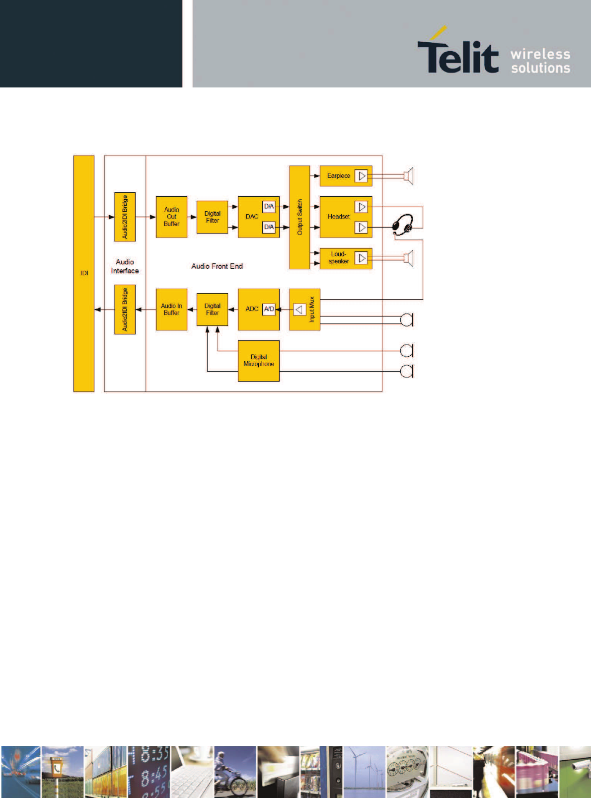
xE922-3GR Hardware User Guide
1VV0301272 Rev.0.8 2017-01-05
Reproduction forbidden without written authorization from Telit Communications S.p.A. - All Rights
Reserved. Page 83 of 112
The following figure shows a top level view of the analog Audio frontend (AFE) of xE92-3GR ABB/PMU.
The IDI connects the ABB to the Audio DSP/DBB.
Note:
All measurements done like described in AES-17 standard method for digital audio engineering. The values
included in the below tables are extracted from to the chipset datasheet.
15.1.1. Analog IN
The audio-in path consists of an input selector, low noise amplifier LNA and following pre-filter with gain
control, second order S-D ADC and finally followed by digital decimator filter. It supports both standard
GSM (BW 4 kHz) and wideband (BW 8 kHz) speech bands as well as full BW for audio recording (16 kHz
and 24 kHz). Overall gain range of the input path goes from -6 dB to +39dB.
As indicated on below block diagram, two mono microphones inputs are available of which one can be
selected at the time, either single ended or differential mode.
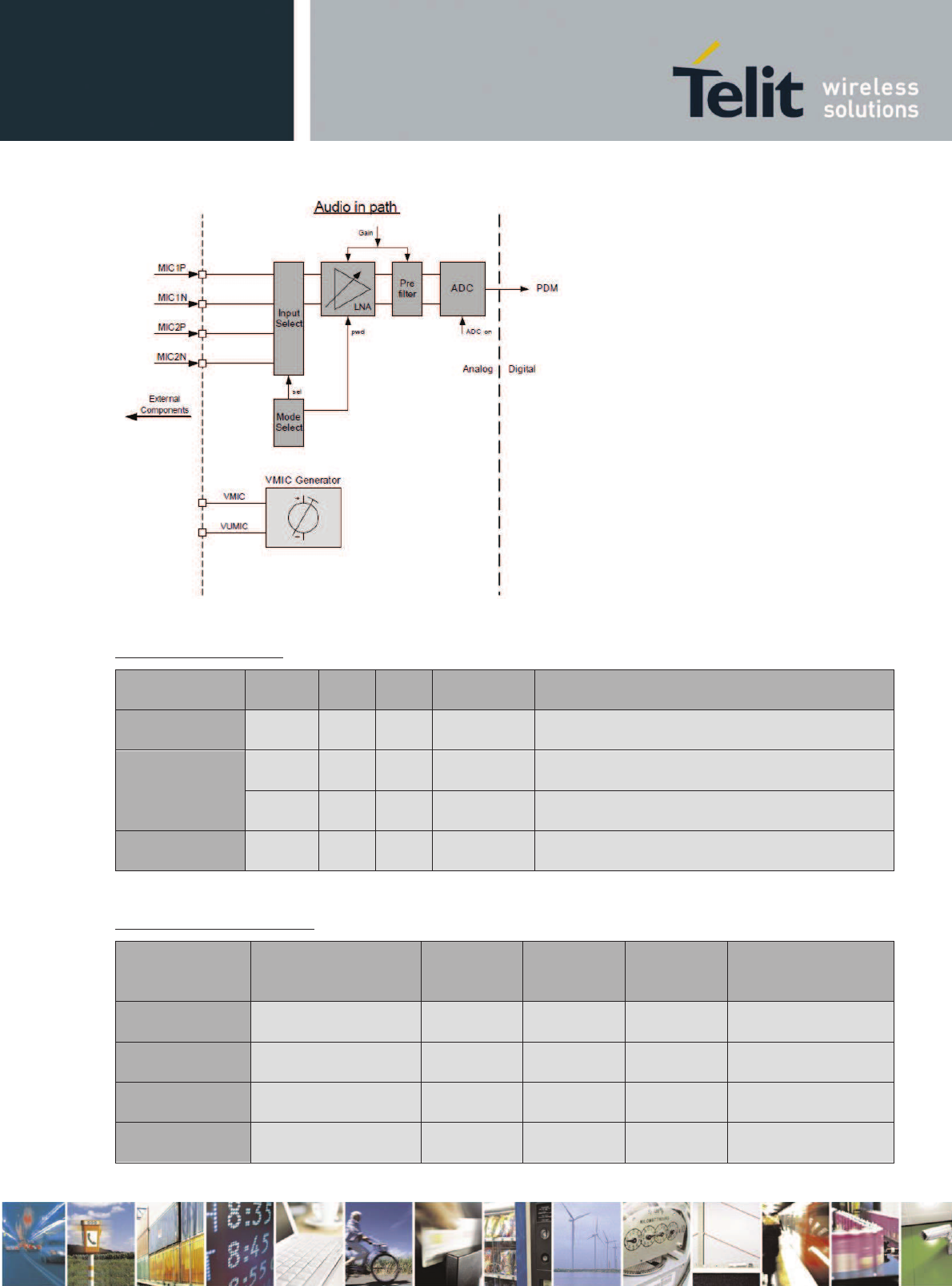
xE922-3GR Hardware User Guide
1VV0301272 Rev.0.8 2017-01-05
Reproduction forbidden without written authorization from Telit Communications S.p.A. - All Rights
Reserved. Page 84 of 112
Parameters audio ADC:
Parameter
Min
Typ
Max
Unit
condition
Bit width
16
bit
BW
20
Hz
Lower limit
4
20
kHz
Upper limit
sample rate
2
4
MHz
Parameters decimation filter
Sample rate fs
mode
Passband
corner
Passband
ripple
Stopband
Stopband attenuation
8 kHz
Narrowband speech
>3.4 kHz
< 1dB
4.0
-
35 kHz
80 dB
16 kHz
Wideband speech
>6.8 kHz
< 1dB
8.0
-
35 kHz
80 dB
32 kHz
music
>14 kHz
< 1dB
16
-
35 kHz
80 dB
48 kHz
CD quality
>20 kHz
< 1dB
24
-
35 kHz
80 dB
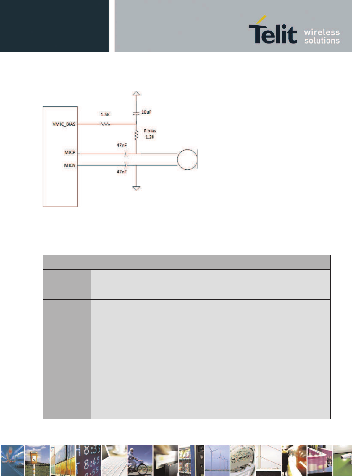
xE922-3GR Hardware User Guide
1VV0301272 Rev.0.8 2017-01-05
Reproduction forbidden without written authorization from Telit Communications S.p.A. - All Rights
Reserved. Page 85 of 112
The following figure shows typical single ended connection concept for electret microphones (AC coupling
value for low cut off frequency @ 300Hz):
The MICP/MICN should be routed close together in order to minimize interference noise.
Differential mode can be interesting when feeding the MIC input from a differential pre-amplifier.
Parameters analog microphone:
Parameter
Min
Typ
Max
Unit
condition
BW
20
Hz
Lower limit
4
20
kHz
Upper limit
DR
72
dB FS
CCIR
Gain 0dB, BW 300
-
8000Hz, input 0.8Vpp diff
THD+N
-55
dB
Ref signal
-10 dB FS
Freq response
-1.2
0.5
dB
Ref signal
-20 dB FS
Input
differential
1.6
Vpp
Gain 0dB, 0 dB FS
R_in
25
kOhm
Differential
C_in
5
10
pF
PSSR
45
66
dB
Gain 0 dB
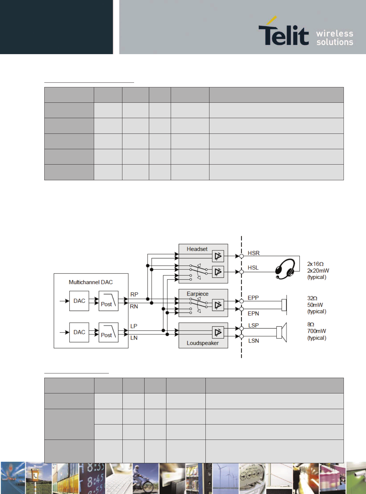
xE922-3GR Hardware User Guide
1VV0301272 Rev.0.8 2017-01-05
Reproduction forbidden without written authorization from Telit Communications S.p.A. - All Rights
Reserved. Page 86 of 112
Parameters VMIC_BIAS supply:
Parameter
Min
Typ
Max
Unit
condition
VMIC_BIAS
1.9..2.2
V
I_out
4.0
mA
Noise
4
uVrms
300
-3900Hz
R_load
1
kOhm
PSSR
75
dB
15.1.2. Analog OUT
The analog audio-out consists of two DAC’s followed by post filter, and finally the output stage. The DAC is
preceeded by digital interpolation filter of which oversampling ratio depends on respective sampling rate.The
following block diagram explains how the output DAC signal sources can be switched to the respective output
driver options.
Parameters audio DAC:
Parameter
Min
Typ
Max
Unit
condition
Bit width
16
bit
BW
20
Hz
Lower limit
4
20
kHz
Upper limit
Output
differential
1.2
Vpp
0 dB FS, gain 0dB
xE922-3GR Hardware User Guide
1VV0301272 Rev.0.8 2017-01-05
Reproduction forbidden without written authorization from Telit Communications S.p.A. - All Rights
Reserved. Page 87 of 112
Parameters interpolation filter
Sample rate fs
mode
Passband
corner
Passband
ripple
Stopband
Stopban
d
atten
uation
8 kHz
Narrowband speech
>3.4 kHz
< 0.5dB
4.6
-
50 kHz
96 dB
16 kHz
Wideband speech
>6.8 kHz
< 0.5dB
9.2
-
50 kHz
96 dB
32 kHz
music
>14 kHz
< 0.5dB
17.6
-
50 kHz
60 dB
48 kHz
CD quality
>20 kHz
< 0.5dB
26.4
-
50 kHz
60 dB
15.1.2.1. Earpiece
The earpiece driver works in differential mode.
Parameters earpiece:
Parameter
Min
Typ
Max
Unit
condition
BW
20
Hz
Lower limit
4
20
kHz
Upper limit
Freq response
-0.5
0.5
dB
20 dB FS ref ampl @997Hz
DR
75
80
dB FS
CCIR
RL=16 ohm, gain +6dB
THD+N
-50
-60
dB
RL=16 ohm, gain +6dB, ref signal
-
10 dB FS
Pout
50
mW
RL=32 ohm
R_load
14
ohm
gain
-12
12
dB
15.1.2.2. Headset
The headset driver contains two single ended outputs (L&R). They are working in bipolar more, i.e. capless
and ground-centred, to avoid large coupling capacitors for a DC-free operation. To support bipolar mode, the
system contains a charge-pump to generate a negative voltage supply.
A click and pop suppression during power on/off sequences is implemented (default enabled)
xE922-3GR Hardware User Guide
1VV0301272 Rev.0.8 2017-01-05
Reproduction forbidden without written authorization from Telit Communications S.p.A. - All Rights
Reserved. Page 88 of 112
Parameters headset:
Parameter
Min
Typ
Max
Unit
condition
BW
20
Hz
Lower limit
4
20
kHz
Upper limit
Freq response
-0.5
0.5
dB
20 dB FS ref ampl @997Hz
DR
85
90
dB FS
CCIR
RL=16 ohm, gain +6dB
THD+N
-50
-60
dB
RL=16 ohm, gain +6dB, ref signal
-
10 dB FS
Vout
2.4
Vpp
RL= 32 ohm
, ground-centered
2.0
Vpp
RL= 16 ohm
, ground-centered
R_load
14
ohm
Gain
-9.1
6
dB
15.1.2.3. Loudspeaker
ClassD amplifier driving a typical load of 8 ohm.
Output stage directly connected to V_BAT, as such max output power depending on V_BAT level, common
mode level = V_BAT/2.
Switching frequency is about 1.2MHz by default, but can be fine-tuned.
For this frequency and the higher harmonics an external filtering has to be applied which could be inherently
done with the connected loudspeaker as well.
Fine tuning allows interference reduction. That means the higher harmonics of the switching frequency can be
moved into areas where the interference with other system components is minimized, and on the other side the
optimum efficiency for the amplifier can be adjusted. If for example interference between the class-D
amplifier switching frequency and the RF-TX carrier is observed, the higher harmonics can be moved to be
exactly on the RF-TX carrier frequency. That would hide the class-D amplifier harmonics. For a RF-RX slot
the higher harmonics can be moved to a different frequency, so that the RF-RX channel is in the middle
between two of the higher harmonic spurs of the class-D amplifier.
xE922-3GR Hardware User Guide
1VV0301272 Rev.0.8 2017-01-05
Reproduction forbidden without written authorization from Telit Communications S.p.A. - All Rights
Reserved. Page 89 of 112
Parameters loudspeaker:
Parameter
Min
Typ
Max
Unit
condition
BW
20
Hz
Lower limit
4
20
kHz
Upper limit
Freq response
-0.5
0.5
dB
20 dB FS ref ampl @997Hz
DR
73
80
dB FS
CCIR
RL=8 ohm, gain 0dB
THD+N
-45
-56
dB
RL=8 ohm, gain 0dB, ref signal
-10 dB FS
Pout
fundamental
wa
ve
700
mW
V_BAT=3.8V,RL= 8 ohm, 10% THD
1200
mW
V_BAT=5.0V,RL= 8 ohm, 10% THD
R_load
8
ohm
Efficiency
80
%
V_BAT=3.8V, load 8 ohm, 125pF, 100uH,
Pout=100mW
PSSR
80
90
dB
Gain
0
24
dB
F_switch
classD
0.6
1.2
2.4
MHz
xE922-3GR Hardware User Guide
1VV0301272 Rev.0.8 2017-01-05
Reproduction forbidden without written authorization from Telit Communications S.p.A. - All Rights
Reserved. Page 90 of 112
15.2. Digital
15.2.1. I2S
As mentioned in the USIF part, USIF1 interface pins , on top of SPI or UART, can be configured as audio I2S
port as well .The below table shows the multiplex pinout in case configured for I2S interface:
USIF1-I2S pin mapping
W5
USIF1_RXD
I
I2S1_RX
CMOS 1.8V
Y5
USIF1_TXD
O
I2S1_TX
CMOS 1.8V
S5
USIF1_SCLK
I/O
I2S1_CLK0
CMOS 1.8V
U5
USIF1_CS
O
I2S1_WA0
CMOS 1.8V
15.2.2. Digital microphone
Digital microphone
AV12
DIG_MIC_CLK
DI
Digital microphone Clock Output
CMOS 1.8V
AN12
DIG_MIC_D1
DI
Digital microphone 1 signal input;
CMOS 1.8V
AT12
DIG_MIC_D2
DI
Digital microphone 2 Clock input;
CMOS 1.8V
AG18
MIC_VDD
AO
MEMC/DIG Microphone Power Supply
power
A stereo MEMS microphone can be connected.
By default DIG_MIC_D1 is sampled at the falling edge of the CLK (configurable).
CLK frequency is minimum 1.96 MHz
Parameters MIC_VDD supply:
Parameter
Min
Typ
Max
Unit
condition
VMIC_BIAS
1.9..2.2
V
I_out
4.0
mA
Noise
4
µ
Vrms
300
-3900Hz
R_load
1
kOhm
PSSR
75
dB

xE922-3GR Hardware User Guide
1VV0301272 Rev.0.8 2017-01-05
Reproduction forbidden without written authorization from Telit Communications S.p.A. - All Rights
Reserved. Page 91 of 112
16. Antenna(s)
The antenna connection and board layout design are the most important parts in the full product
design and they strongly reflect on the product’s overall performance. Read carefully and
follow the requirements and the guidelines for a good and proper design.
16.1. GSM/WCDMA Antenna Requirements
The antenna for a Telit xE922-3GR device must fulfill the following requirements:
When using the Telit xE922-3GR, since there’s no antenna connector on the module, the
antenna must be connected to the xE922-3GR antenna pad by means of a transmission line
implemented on the PCB.
In the case that the antenna is not directly connected to the antenna pad of the xE922-3GR, then
a PCB line is required in order to connect with it or with its connector.
This transmission line shall fulfill the following requirements:
Antenna Line on PCB Requirements
Characteristic Impedance
50Ohm
Max Attenuation
0.3dB
Coupling with other signals shall be avoided
Cold End (Ground Plane) of antenna shall be equipotential to the xE922-3GR ground pads
Furthermore if the device is developed for the US and/or Canada market, it must comply with
the FCC and/or IC approval requirements:
This device is to be used only for mobile and fixed application. The antenna(s) used for this
transmitter must be installed to provide a separation distance of at least 20 cm from all persons
and must not be co-located or operating in conjunction with any other antenna or transmitter.
End-Users must be provided with transmitter operation conditions for satisfying RF exposure
compliance. OEM integrators must ensure that the end user has no manual instructions to
GSM / WCDMA Antenna Requirements
Frequency range
Depending on the frequency bands provided by the network operator, and of
those, w
hich subset of band set the
OEM may support while using the Telit
module, the customer must use the most suitable antenna for covering those
bands.
The bands supported by Telit
xE922-3GR
module family are given in Section
2.3
Gain
Maximum Gain in 1900 MHz band = 2.5 dBi
Maximum Gain in 850 MHz band = -1.54 dBi
Impedance
50 Ohm
Input power
> 33dBm(2 W) peak power in GSM
> 24dBm Average power in WCDMA
VSWR absolute max
<= 10:1
VSWR recommended
<= 2:1

xE922-3GR Hardware User Guide
1VV0301272 Rev.0.8 2017-01-05
Reproduction forbidden without written authorization from Telit Communications S.p.A. - All Rights
Reserved. Page 92 of 112
remove or install the xE922-3GR module. Antennas used for this OEM module must not exceed
3dBi gain for mobile and fixed operating configurations.
16.1.1. GSM/WCDMA Antenna – PCB line Guidelines
· Make sure that the transmission line’s characteristic impedance is 50ohm.
· Keep the line on the PCB as short as possible since the antenna line loss should be less than
around 0.3dB.
· Line geometry should have uniform characteristics, constant cross section, avoid meanders
and abrupt curves.
· Any suitable geometry/structure can be used for implementing the printed transmission line
affecting the antenna.
· If a Ground plane is required in the line geometry, that plane must be continuous and
sufficiently extended so the geometry can be as similar as possible to the related canonical
model.
· Keep, if possible, at least one layer of the PCB used only for the Ground plane; if possible,
use this layer as reference Ground plane for the transmission line.
· It is wise to surround (on both sides) the PCB transmission line with Ground. Avoid having
other signal traces facing directly the antenna line trace.
· Avoid crossing any un-shielded transmission line footprint with other traces on different
layers.
· The Ground surrounding the antenna line on the PCB must be strictly connected to the
main Ground plane by means of via-holes (once per 2mm at least) placed close to the
ground edges facing the line trace.
· Place EM-noisy devices as far as possible from xE922-3GR antenna line.
· Keep the antenna line far away from the xE922-3GR power supply lines.
· If EM-noisy devices are present on the PCB hosting the xE922-3GR, such as fast switching
ICs, take care to shield them with a metal frame cover.
· If EM-noisy devices are not present around the line, using geometries such as Micro strip
or Grounded Coplanar Waveguide is preferred since they typically ensure less attenuation
compared to a Strip line having the same length.
16.1.2. GSM/WCDMA Antenna – Installation Guidelines
· Install the antenna in a location with access to the network radio signal.
· If the chosen antenna is a style which requires a ground plane, ensure that it is
properly attached, both electrically and mechanically, to a ground plane with
dimensions and mechanical structure as recommended by the antenna manufacturer
· The antenna must be installed such that it provides a separation distance of at least 20
cm from all persons and must not be co-located or operating in conjunction with any
other antenna or transmitter;
· The antenna must not be installed inside metal cases;
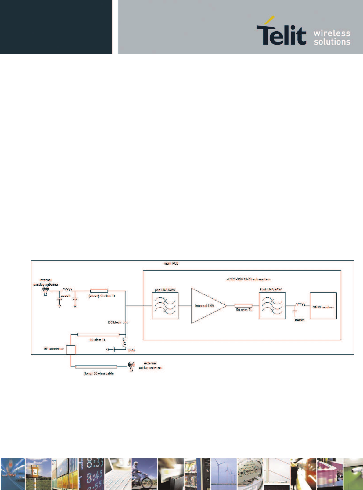
xE922-3GR Hardware User Guide
1VV0301272 Rev.0.8 2017-01-05
Reproduction forbidden without written authorization from Telit Communications S.p.A. - All Rights
Reserved. Page 93 of 112
16.2. WiFi/BT Antenna Requirements
Antenna recommended specification:
· Frequency: 2.4-2.5GHz
· Gain (peak): 2.3 dBi
· VSWR : max 1.8
· Return loss : max -10 dB
· Radiation : omni directional
· Polarization : linear vertical
· Power handling : 1W
· Impedance 50 ohm
16.3. GNSS Antenna Requirements
The GNSS subsystem of xE922-3GR module is visualized on below block diagram.
The module features ‘internal’ pre-LNA_SAW / LNA / post-LNA_SAW RF chain in front of
the GNSS receiver.
Two possible GNSS antenna scenarios are possible on the application main board:
· Internal ‘passive’ antenna
· External ‘active’ antenna
Both scenarios are drawn in the figure, only one should be applied.

xE922-3GR Hardware User Guide
1VV0301272 Rev.0.8 2017-01-05
Reproduction forbidden without written authorization from Telit Communications S.p.A. - All Rights
Reserved. Page 94 of 112
In case of an internal antenna configuration, it is important to keep the 50 ohm transmission
line (TL) short to limit possible signal degradation between antenna and internal LNA amplifier.
In case of an active external antenna, a bias circuit to feed the antenna integrated LNA is
required. An inductor filter is used as RF block. Also a DC-block capacitor is required in order
to keep unwanted DC voltage away from the internal RF FE devices.
Care should be taken to minimize stubs on the 50ohm PCB structure because of placement of
these additional bias components.
16.3.1. Combined GNSS Antenna
The use of combined RF/GNSS antenna is NOT recommended. This solution could generate
extremely poor GNSS reception. In addition, the combination of antennas requires an additional
diplexer, which adds significant power losses in the RF path.
16.3.2. Linear and Patch GNSS Antenna
Using linear type of antenna introduces at least 3dB of loss compared to a circularly polarized
(CP) antenna. Having a spherical gain response instead of a hemispherical gain response could
aggravate the multipath behavior & create poor position accuracy.
16.3.3. Front End Design Considerations
When using the Telit xE922-3GR, since there is no antenna connector on the module, the
antenna must be connected to the xE922-3GR through the PCB to the antenna pad.
In the case that the antenna is not directly connected at the antenna pad of the xE922-3GR, then
a PCB line is required.
This line of transmission shall fulfill the following requirements:
Antenna Line on PCB Requirements
Characteristic Impedance
50Ohm
Max Attenuation
0.3dB
Coupling with
other signals shall be avoided
Cold End (Ground Plane) of antenna shall
be equipotential to the xE922-3GR
ground pads
Furthermore if the device is developed for the US and/or Canada market, it must comply with
the FCC and/or IC requirements.
This device is to be used only for mobile and fixed application.

xE922-3GR Hardware User Guide
1VV0301272 Rev.0.8 2017-01-05
Reproduction forbidden without written authorization from Telit Communications S.p.A. - All Rights
Reserved. Page 95 of 112
16.3.4. GNSS Antenna - PCB Line Guidelines
· Ensure that the antenna line impedance is 50ohm.
· Keep the line on the PCB as short as possible to reduce the loss.
· The antenna line must have uniform characteristics, constant cross section, avoiding
meanders and abrupt curves.
· Keep one layer of the PCB used only for the Ground plane; if possible.
· Surround (on the sides, over and under) the antenna line on the PCB with Ground. Avoid
having other signal traces in proximity of the transmission line where coupling may occur.
· The Ground around the antenna line on the PCB must be strictly connected to the main
Ground plane by placing vias at least once per 2mm.
· Place EM-noisy devices as far as possible from xE922-3GR antenna line.
· Keep the antenna line far away from the xE922-3GR power supply lines.
· If EM-noisy devices are around the PCB hosting the xE922-3GR, such as fast switching
ICs, ensure shielding the antenna line by burying it inside the layers of PCB and
surrounding it with Ground planes; or shield it with a metal frame cover.
· If you do not have EM-noisy devices around the PCB of xE922-3GR, use a Micro strip line
on the surface copper layer for the antenna line. The line attenuation will be lower than a
buried one.
16.3.5. GNSS Antenna – Installation Guidelines
· The xE922-3GR, due to its sensitivity characteristics, is capable of performing a fix inside
buildings. (In any case the sensitivity could be affected by the building characteristics i.e.
shielding)
· If the chosen antenna is a style which requires a ground plane, ensure that it is properly
attached, both electrically and mechanically, to a ground plane with dimensions and
mechanical structure as recommended by the antenna manufacturer
· The antenna must not be co-located or operating in conjunction with any other antenna or
transmitter.
· The antenna shall not be installed inside metal cases.
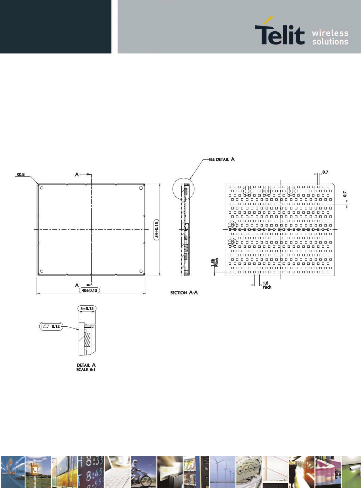
xE922-3GR Hardware User Guide
1VV0301272 Rev.0.8 2017-01-05
Reproduction forbidden without written authorization from Telit Communications S.p.A. - All Rights
Reserved. Page 96 of 112
17. Mounting the module on your board
17.1. General
The xE922-3GR module is designed to be compliant with a standard lead-free SMT process
17.2. Finishing & Dimensions
Board finsih : ENIG (Electroless Nickel Immersion Gold)
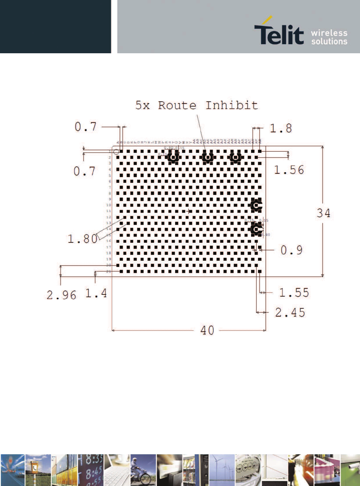
xE922-3GR Hardware User Guide
1VV0301272 Rev.0.8 2017-01-05
Reproduction forbidden without written authorization from Telit Communications S.p.A. - All Rights
Reserved. Page 97 of 112
17.3. Recommended foot print for the application main board
441 pads
transparant top view
Dimensions are in [mm].In order to easily rework the xE922-3GR it is suggested to consider
that the application has a 1.5 mm placement inhibit area around the module.
It is also suggested, as a common rule for an SMT component, to avoid having a mechanical
part of the application in direct contact with the module.
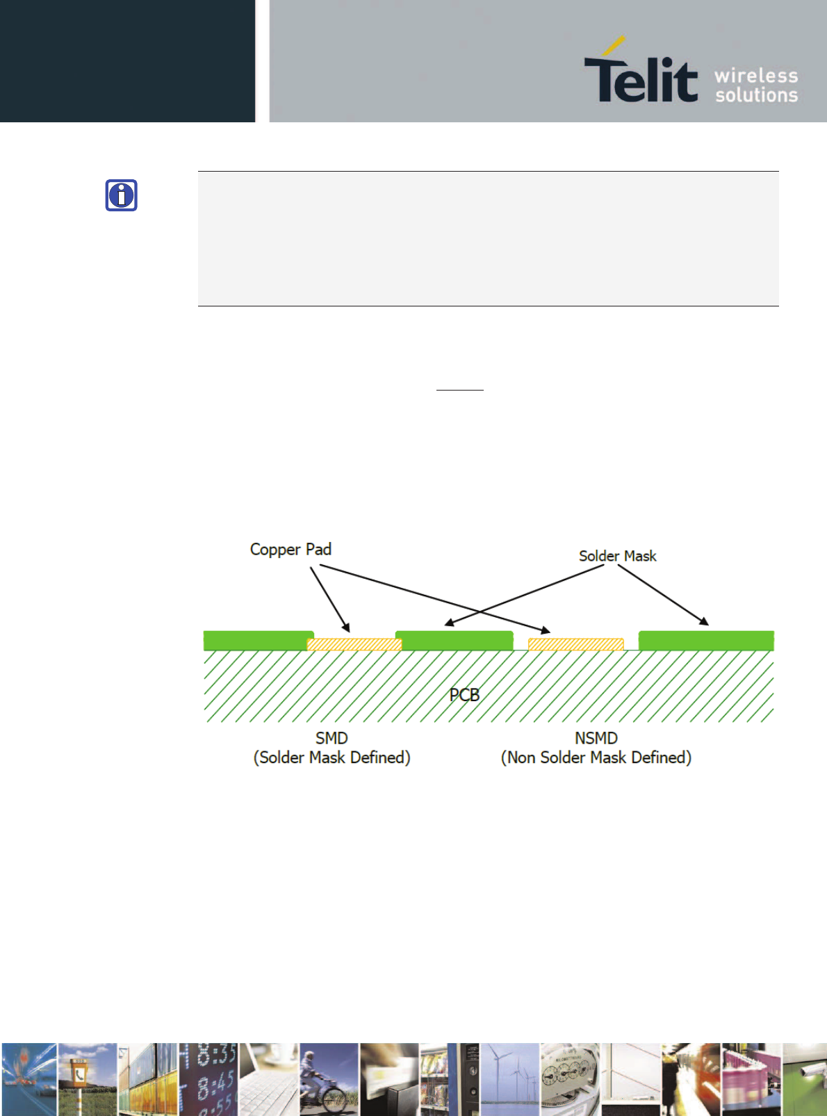
xE922-3GR Hardware User Guide
1VV0301272 Rev.0.8 2017-01-05
Reproduction forbidden without written authorization from Telit Communications S.p.A. - All Rights
Reserved. Page 98 of 112
NOTE:
In the customer application, the region under ROUTE INHIBIT (see figure above) must be
clear from signal. The five horseshoe shapes, indicated in the footprint picture above, are solder
resist mask openings in the surrounding GND copper fill. They provide proper GND connection
for built-in RF probes on Telit’s production test jig socket. It is not intended to replicate these
horseshoe shapes as well on the customer’s module carrier board implementation, the GND
pads surrounding the antenna pads provide solid RF GND.
17.4. Stencil
Stencil’s apertures layout can be the same as the recommended footprint (1:1). A suggested
thickness of stencil foil is greater than 150 µm.
17.5. PCB Pad Design
Non solder mask defined (NSMD) type is recommended for the solder pads on the PCB.
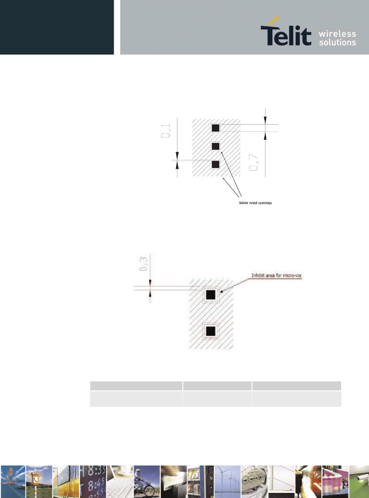
xE922-3GR Hardware User Guide
1VV0301272 Rev.0.8 2017-01-05
Reproduction forbidden without written authorization from Telit Communications S.p.A. - All Rights
Reserved. Page 99 of 112
17.6. Recommendations for PCB Pad Dimensions (mm)
It is not recommended to place via or micro-via, which are not covered by solder resist in an
area of 0.3 mm around the pads unless it carries the same signal of the pad itself (see following
figure).
Holes in pad are allowed only for blind holes and not for through holes.
Recommendations for PCB Pad Surfaces:
Finish
Layer thickness (um)
Properties
Electro
-
less Ni / Immersion Au
3 –
7 / 0.05 – 0.15
good solder ability protection,
high shear force values
The PCB must be able to resist the higher temperatures which occur during the lead-free
process. This issue should be discussed with the PCB-supplier. Generally, the wettability of tin-
lead solder paste on the described surface plating is better compared to lead-free solder paste.
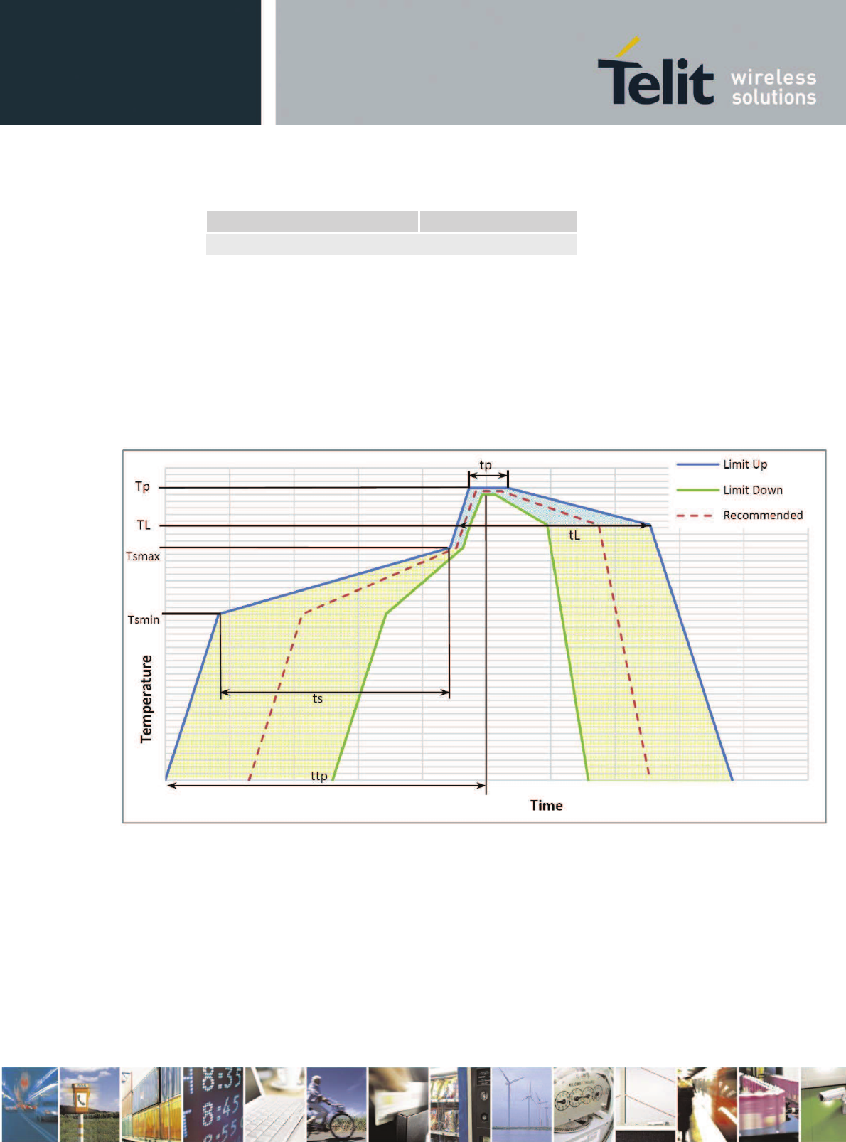
xE922-3GR Hardware User Guide
1VV0301272 Rev.0.8 2017-01-05
Reproduction forbidden without written authorization from Telit Communications S.p.A. - All Rights
Reserved. Page 100 of 112
17.7. Solder Paste
Solder Paste
Lead free
Sn/Ag/Cu
We recommend using only “no clean” solder paste in order to avoid the cleaning of the modules
after assembly.
17.7.1. Solder Reflow
Recommended solder reflow profile is shown below:
xE922-3GR Hardware User Guide
1VV0301272 Rev.0.8 2017-01-05
Reproduction forbidden without written authorization from Telit Communications S.p.A. - All Rights
Reserved. Page 101 of 112
Profile Feature
Pb-Free Assembly
Average ramp-up rate (TL to TP)
3°C/second max
Preheat
–
Temperature Min (Tsmin)
–
Temperature Max (Tsmax)
– Time (min to max) (ts)
150°C
200°C
60-180 seconds
Tsmax to TL
– Ramp-up Rate
3°C/second max
Time maintained above:
–
Temperature (TL)
– Time (tL)
217°C
60-150 seconds
Peak Temperature (Tp)
245 +0/-5°C
Time within 5°C of actual Peak
Temperature (tp)
10-30 seconds
Ramp-down Rate
6°C/second max.
Time 25°C to Peak Temperature
8 minutes max.
NOTE:
All temperatures refer to topside of the package, measured on the package body surface.
WARNING:
The xE922-3GR module withstands one reflow process only.
xE922-3GR Hardware User Guide
1VV0301272 Rev.0.8 2017-01-05
Reproduction forbidden without written authorization from Telit Communications S.p.A. - All Rights
Reserved. Page 102 of 112
18. Packing system
The Telit xE922-3GR module is packaged on trays.
The tray is JEDEC compliant, injection molded antistatic Modified Polyphenylene ether (MPPO). It has good
thermal characteristics and can withstand a the standard baking temperature up to 125°C, thereby avoiding
handling the modules if baking is required. The trays are rigid, thus providing more mechanical protection
against transport stress. Additionally they are re-usable and so environmentally sustainable.
There are 2 (two) antistatic rubber bands that enclose each envelope.
The carton box is rigid, thus offering mechanical protection. The carton box has one flap across the whole top
surface. It is sealed with tape along the edges of the box.
Tray
in each
tray
inside each
envelope
inside each
carton box
Modules/tray
Description
modules/
tray
trays/
envelope
modules/
envelope
envelopes/
carton box
modules/
box
xE922-3GR
packaging
JEDEC Tray
24
5+ 1 empty
120
4 480
Qty
Minimum Order
Quantity (MOQ)
120
Standard Packing
Quantity (SPQ)
480
Each tray contains 24 pieces as shown in the following picture:
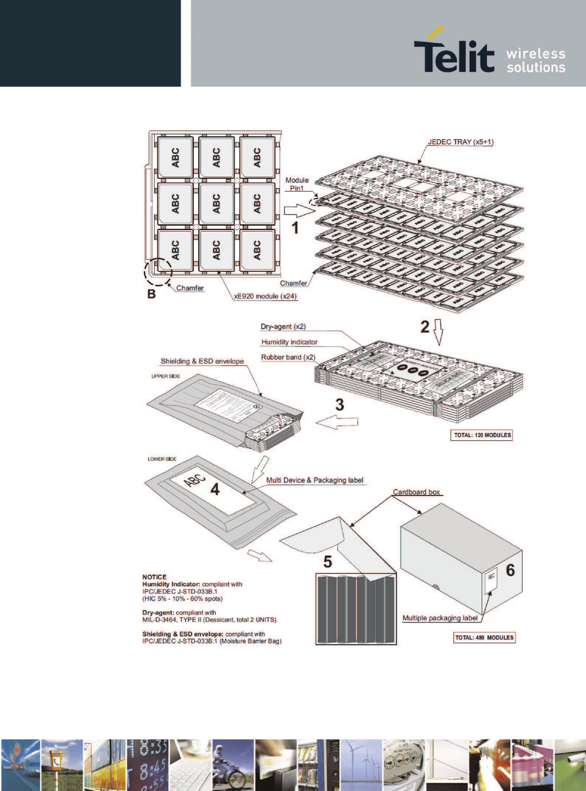
xE922-3GR Hardware User Guide
1VV0301272 Rev.0.8 2017-01-05
Reproduction forbidden without written authorization from Telit Communications S.p.A. - All Rights
Reserved. Page 103 of 112
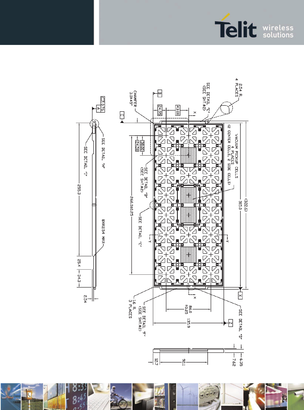
xE922-3GR Hardware User Guide
1VV0301272 Rev.0.8 2017-01-05
Reproduction forbidden without written authorization from Telit Communications S.p.A. - All Rights
Reserved. Page 104 of 112
18.1. Tray Drawing

xE922-3GR Hardware User Guide
1VV0301272 Rev.0.8 2017-01-05
Reproduction forbidden without written authorization from Telit Communications S.p.A. - All Rights
Reserved. Page 105 of 112
18.2. Moisture Sensitivity
The xE922-3GR is a Moisture Sensitive Device level 3, in accordance with standard
IPC/JEDEC J-STD-020. Observe all of the requirements for using this kind of components.

xE922-3GR Hardware User Guide
1VV0301272 Rev.0.8 2017-01-05
Reproduction forbidden without written authorization from Telit Communications S.p.A. - All Rights
Reserved. Page 106 of 112
19. Safety Recommendations
READ CAREFULLY
Be sure that the use of this product is allowed in your country and in the environment required.
The use of this product may be dangerous and must be avoided in the following areas:
· Where it can interfere with other electronic devices in environments such as
hospitals, airports, aircrafts, etc.
· Where there is risk of explosion such as gasoline stations, oil refineries, etc.
It is the responsibility of the user to enforce the country regulations and the specific
environment regulations.
Do not disassemble the product; any mark of tampering will compromise the warranty validity.
We recommend following the instructions of the hardware user guides for correct wiring of the
product. The product must be supplied with a stabilized voltage source and the wiring conform
to the security and fire prevention regulations.
The product must be handled with care, avoiding any contact with the pins because electrostatic
discharges may damage the product itself. The same caution must be taken for the SIM,
checking carefully the instructions for its use. Do not insert or remove the SIM when the product
is in power saving mode.
The system integrator is responsible for the functioning of the final product; therefore, care
must be taken of the external components of the module, as well as of any project or installation
issue, because of the risk of disturbing the GSM network or external devices or having any
impact on safety. Should there be any doubt, please refer to the technical documentation and
the regulations in force.
Every module must be equipped with a proper antenna with the specified characteristics. The
antenna must be installed with care in order to avoid any interference with other electronic
devices and must be installed with the guarantee of a minimum 20 cm distance from a human
body. In case this requirement cannot be satisfied, the system integrator must assess the final
product against the SAR regulation.
The European Community provides some Directives for electronic equipment introduced on
the market. All the relevant information is available on the European Community website:
http://europa.eu.int/comm/enterprise/rtte/dir99-5.htm
The text of the Directive 99/05 regarding telecommunication equipment is available, while the
applicable Directives (Low Voltage and EMC) are available at:
http://europa.eu.int/comm/enterprise/rtte/dir99-5.htm
The equipment is intended to be installed in restricted area locations.
The equipment must be supplied by an external limited power source in compliance with the
clause 2.5 of the standard IEC 60950-1.
Ambient working temperature for the temperature test of the standard EN 60950-1: +50 ºC

xE922-3GR Hardware User Guide
1VV0301272 Rev.0.8 2017-01-05
Reproduction forbidden without written authorization from Telit Communications S.p.A. - All Rights
Reserved. Page 107 of 112
20. Conformity assessment issues
20.1. FCC/IC Regulatory notices
20.1.1. Modification statement
Telit Communications S.p.A has not approved any changes or modifications to this device by the user.
Any changes or modifications could void the user’s authority to operate the equipment.
Telit Communications S.p.A n’approuve aucune modification apportée à l’appareil par l’utilisateur,
quelle qu’en soit la nature. Tout changement ou modification peuvent annuler le droit d’utilisation de
l’appareil par l’utilisateur.
20.1.2. Interference statement
This device complies with Part 15 of the FCC Rules and Industry Canada licence-exempt RSS
standard(s). Operation is subject to the following two conditions: (1) this device may not cause
interference, and (2) this device must accept any interference, including interference that may cause
undesired operation of the device.
Le présent appareil est conforme aux CNR d'Industrie Canada applicables aux appareils radio exempts
de licence. L'exploitation est autorisée aux deux conditions suivantes : (1) l'appareil ne doit pas
produire de brouillage, et (2) l'utilisateur de l'appareil doit accepter tout brouillage radioélectrique
subi, même si le brouillage est susceptible d'en compromettre le fonctionnement.
20.1.3. RF exposure
This equipment complies with FCC and IC radiation exposure limits set forth for an uncontrolled
environment. The antenna should be installed and operated with minimum distance of 20 cm between
the radiator and your body. Antenna gain must be below:
Frequency range
Type of
antenna
Antenna gain
850 MHz band
N/A
4.37 dBi
1900 MHz band
N/A
2.11 dBi
2.4 G
Hz band
Half-wave
dipole antenna
2.3 dBi
This transmitter must not be co-located or operating in conjunction with any other antenna or transmitter.

xE922-3GR Hardware User Guide
1VV0301272 Rev.0.8 2017-01-05
Reproduction forbidden without written authorization from Telit Communications S.p.A. - All Rights
Reserved. Page 108 of 112
Cet appareil est conforme aux limites d'exposition aux rayonnements de la IC pour un environnement
non contrôlé. L'antenne doit être installé de façon à garder une distance minimale de 20 centimètres
entre la source de rayonnements et votre corps. Gain de l'antenne doit être ci-dessous:
Bande de fréquence
Type d’
antenne
Gain de l'antenne
850 MHz band
N/A
4.37 dBi
1900 MHz band
N/A
2.11 dBi
2.4 GHz band
Antenne dipole
demi-onde
2.3 dBi
L'émetteur ne doit pas être colocalisé ni fonctionner conjointement avec à autre antenne ou autre
émetteur.
20.1.4. FCC Class B digital device notice
This equipment has been tested and found to comply with the limits for a Class B digital device,
pursuant to part 15 of the FCC Rules. These limits are designed to provide reasonable protection against
harmful interference in a residential installation. This equipment generates, uses and can radiate radio
frequency energy and, if not installed and used in accordance with the instructions, may cause harmful
interference to radio communications. However, there is no guarantee that interference will not occur
in a particular installation. If this equipment does cause harmful interference to radio or television
reception, which can be determined by turning the equipment off and on, the user is encouraged to try
to correct the interference by one or more of the following measures:
- Reorient or relocate the receiving antenna.
- Increase the separation between the equipment and receiver.
- Connect the equipment into an outlet on a circuit different from that to which the receiver is
connected.
- Consult the dealer or an experienced radio/TV technician for help.
20.1.5. Labelling Requirements for the Host device
The host device shall be properly labelled to identify the modules within the host device. The
certification label of the module shall be clearly visible at all times when installed in the host device,
otherwise the host device must be labelled to display the FCC ID and IC of the module, preceded by
the words "Contains transmitter module", or the word "Contains", or similar wording expressing the
same meaning, as follows:
Contains FCC ID: RI7HE9223GR
Contains IC: 5131A-HE9223GR
L'appareil hôte doit être étiqueté comme il faut pour permettre l'identification des modules qui s'y
trouvent. L'étiquette de certification du module donné doit être posée sur l'appareil hôte à un endroit
bien en vue en tout temps. En l'absence d'étiquette, l'appareil hôte doit porter une étiquette donnant le

xE922-3GR Hardware User Guide
1VV0301272 Rev.0.8 2017-01-05
Reproduction forbidden without written authorization from Telit Communications S.p.A. - All Rights
Reserved. Page 109 of 112
FCC ID et l’IC du module, précédé des mots « Contient un module d'émission », du mot « Contient »
ou d'une formulation similaire exprimant le même sens, comme suit:
Contains FCC ID: RI7HE9223GR
Contains IC: 5131A-HE9223GR
CAN ICES-3 (B) / NMB-3 (B)
This Class B digital apparatus complies with Canadian ICES-003.
Cet appareil numérique de classe B est conforme à la norme canadienne ICES-003.
20.2. 1999/5/EC Directive
This device has been evaluated against the essential requirements of the 1999/5/EC Directive.
Bulgarian
С настоящето “Telit Communications S.P.A.” декларира, че “xE922-3GR module” отговаря на съществените
изисквания и другите приложими изисквания на Директива 1999/5/ЕС.
Croatian
Ovime “Telit Communications S.P.A.”, izjavljuje da je ovaj “xE922-3GR module” je u skladu s osnovnim zahtjevima i
drugim relevantnim odredbama Direktive 1999/5/EC.
Czech
“Telit Communications S.P.A.” tímto prohlašuje, že tento “xE922-3GR module” je ve shodě se základními požadavky
a dalšími příslušnými ustanoveními směrnice 1999/5/ES.
Danish
Undertegnede “Telit Communications S.P.A.” erklærer herved, at følgende udstyr “xE922-3GR module” overholder de
væsentlige krav og øvrige relevante krav i direktiv 1999/5/EF.
Dutch
Hierbij verklaart “Telit Communications S.P.A.” dat het toestel “xE922-3GR module” in overeenstemming is met de
essentiële eisen en de andere relevante bepalingen van richtlijn 1999/5/EG.
English
Hereby, “Telit Communications S.P.A.”, declares that this “xE922-3GR module” is in compliance with the essential
requirements and other relevant provisions of Directive 1999/5/EC.
Estonian
Käesolevaga kinnitab “Telit Communications S.P.A.” seadme “xE922-3GR module” vastavust direktiivi 1999/5/EÜ
põhinõuetele ja nimetatud direktiivist tulenevatele teistele asjakohastele sätetele.
German
Hiermit erklärt “Telit Communications S.P.A.”, dass sich das Gerät “xE922-3GR module” in Übereinstimmung mit den
grundlegenden Anforderungen und den übrigen einschlägigen Bestimmungen der Richtlinie 1999/5/EG befindet.
Greek
ΜΕ ΤΗΝ ΠΑΡΟΥΣΑ “Telit Communications S.P.A.” ΔΗΛΩΝΕΙ ΟΤΙ “xE922-3GR module” ΣΥΜΜΟΡΦΩΝΕΤΑΙ
ΠΡΟΣ ΤΙΣ ΟΥΣΙΩΔΕΙΣ ΑΠΑΙΤΗΣΕΙΣ ΚΑΙ ΤΙΣ ΛΟΙΠΕΣ ΣΧΕΤΙΚΕΣ ΔΙΑΤΑΞΕΙΣ ΤΗΣ ΟΔΗΓΙΑΣ 1999/5/ΕΚ.
Hungarian
Alulírott, “Telit Communications S.P.A.” nyilatkozom, hogy a “xE922-3GR module” megfelel a vonatkozó alapvetõ
követelményeknek és az 1999/5/EC irányelv egyéb elõírásainak.
Finnish
“Telit Communications S.P.A.” vakuuttaa täten että “xE922-3GR module” tyyppinen laite on direktiivin 1999/5/EY
oleellisten vaatimusten ja sitä koskevien direktiivin muiden ehtojen mukainen.
French
Par la présente “Telit Communications S.P.A.” déclare que l'appareil “xE922-3GR module” est conforme aux
exigences essentielles et aux autres dispositions pertinentes de la directive 1999/5/CE.
Icelandic
Hér með lýsir “Telit Communications S.P.A.” yfir því að “xE922-3GR module” er í samræmi við grunnkröfur og aðrar
kröfur, sem gerðar eru í tilskipun 1999/5/EC
Italian
Con la presente “Telit Communications S.P.A.” dichiara che questo “xE922-3GR module” è conforme ai requisiti
essenziali ed alle altre disposizioni pertinenti stabilite dalla direttiva 1999/5/CE.
Latvian
Ar šo “Telit Communications S.P.A.” deklarē, ka “xE922-3GR module” atbilst Direktīvas 1999/5/EK būtiskajām
prasībām un citiem ar to saistītajiem noteikumiem.
Lithuanian
Šiuo “Telit Communications S.P.A.” deklaruoja, kad šis “xE922-3GR module” atitinka esminius reikalavimus ir kitas
1999/5/EB Direktyvos nuostatas.

xE922-3GR Hardware User Guide
1VV0301272 Rev.0.8 2017-01-05
Reproduction forbidden without written authorization from Telit Communications S.p.A. - All Rights
Reserved. Page 110 of 112
Maltese
Hawnhekk, “Telit Communications S.P.A.”, jiddikjara li dan “xE922-3GR module” jikkonforma mal-ħtiġijiet essenzjali
u ma provvedimenti oħrajn relevanti li hemm fid-Dirrettiva 1999/5/EC.
Norwegian
“Telit Communications S.P.A.” erklærer herved at utstyret “xE922-3GR module” er i samsvar med de grunnleggende
krav og øvrige relevante krav i direktiv 1999/5/EF.
Polish
Niniejszym “Telit Communications S.P.A.” oświadcza, że “xE922-3GR module” jest zgodny z zasadniczymi
wymogami oraz pozostałymi stosownymi postanowieniami Dyrektywy 1999/5/EC
Portuguese
“Telit Communications S.P.A.” declara que este “xE922-3GR module” está conforme com os requisitos essenciais e
outras disposições da Directiva 1999/5/CE.
Slovak
“Telit Communications S.P.A.” týmto vyhlasuje, že “OM12030/X00” (*) spĺňa základné požiadavky a všetky príslušné
ustanovenia Smernice 1999/5/ES.
Slovenian
“Telit Communications S.P.A.” izjavlja, da je ta “xE922-3GR module” v skladu z bistvenimi zahtevami in ostalimi
relevantnimi določili direktive 1999/5/ES.
Spanish
Por medio de la presente “Telit Communications S.P.A.” declara que “xE922-3GR module” cumple con los requisitos
esenciales y cualesquiera otras disposiciones aplicables o exigibles de la Directiva 1999/5/CE.
Swedish
Härmed intygar “Telit Communications S.P.A.” att denna “xE922-3GR module” står I överensstämmelse med de
väsentliga egenskapskrav och övriga relevanta bestämmelser som framgår av direktiv 1999/5/EG.
In order to satisfy the essential requirements of R&TTE Directive (1999/5/EC), the product is
compliant with the following standards:
Electrical Safety (Art. 3(1)(a)):
EN 60950-1:2006 + A11:2009 + A1:2010 +
A12:2011 + AC:2011 + A2:2013
EMF Exposure (Art. 3(1)(a)):
EN 62311:2008
EMC (Art. 3(1)(b)):
EN 301 489-1 V1.9.2
EN 301 489
-3 V1.6.1
EN 301 489
-7 V1.3.1
EN 301 489
-17 V2.2.1
EN 301 489
-24 V1.5.1
Radio Spectrum Use (Art. 3(2)):
EN 301 511 V12.1.1
EN 301 908
-1 V7.1.1
EN 301 908
-02 V6.2.1
ETSI EN 300 440
-1 V1.6.1
ETSI EN 300 440
-2 V1.4.1
ETSI EN 300 328 V1.9.1
The conformity assessment procedure referred to in Article 10 and detailed in Annex IV of Directive
1999/5/EC has been followed with the involvement of the following Notified Body:
AT4 wireless, S.A.
Parque Tecnologico de Andalucía
C/ Severo Ochoa 2
29590 Campanillas – Málaga
SPAIN
Notified Body No: 1909
Thus, the following marking is included in the product:
xE922-3GR Hardware User Guide
1VV0301272 Rev.0.8 2017-01-05
Reproduction forbidden without written authorization from Telit Communications S.p.A. - All Rights
Reserved. Page 111 of 112
There is no restriction for the commercialization of this device in all the countries of the European
Union.
Final product integrating this module must be assessed against essential requirements of the
1999/5/EC (R&TTE) Directive. It should be noted that assessment does not necessarily lead to
testing. Telit Communications S.p.A. recommends carrying out the following assessments:
RF spectrum use (R&TTE art 3.2)
It will depend on the antenna used on the final product
EMC (R&TTE art 3.1b)
Testing
Health & Safety (R&TTE art 3.1a)
Testing
xE922-3GR Hardware User Guide
1VV0301272 Rev.0.8 2017-01-05
Reproduction forbidden without written authorization from Telit Communications S.p.A. - All Rights
Reserved. Page 112 of 112
21. Document History
Revision
Date
Changes
0.1
2016-05-18
Draft
0.2
2016-06-03
0.3
2016-06-10
0.4
2016-07-19
0.5
2016-08-17
0.6
2016-09-29
Added typical power consumption table
0.7
2016-10-26
Update pwr consumption
0.8
2017-01-
05
Update 60950 safety remarks
Add Conformity Assessment Issues chapter
Update on LGA pin AN8