Telit Communications S p A XE61 Wireless module 2.4GHz ZE61/LE61/XE61-2.4 User Manual Revised manual
Telit Communications S.p.A. Wireless module 2.4GHz ZE61/LE61/XE61-2.4 Revised manual
UserManual.wiki
>
Telit Communications S p A
>
XE61 User Manual
Revised manual
Navigation menu
Upload a User Manual
Namespaces
Wiki Guide
HTML
PDF
Info
Views
User Manual
Discussion / Help
Navigation

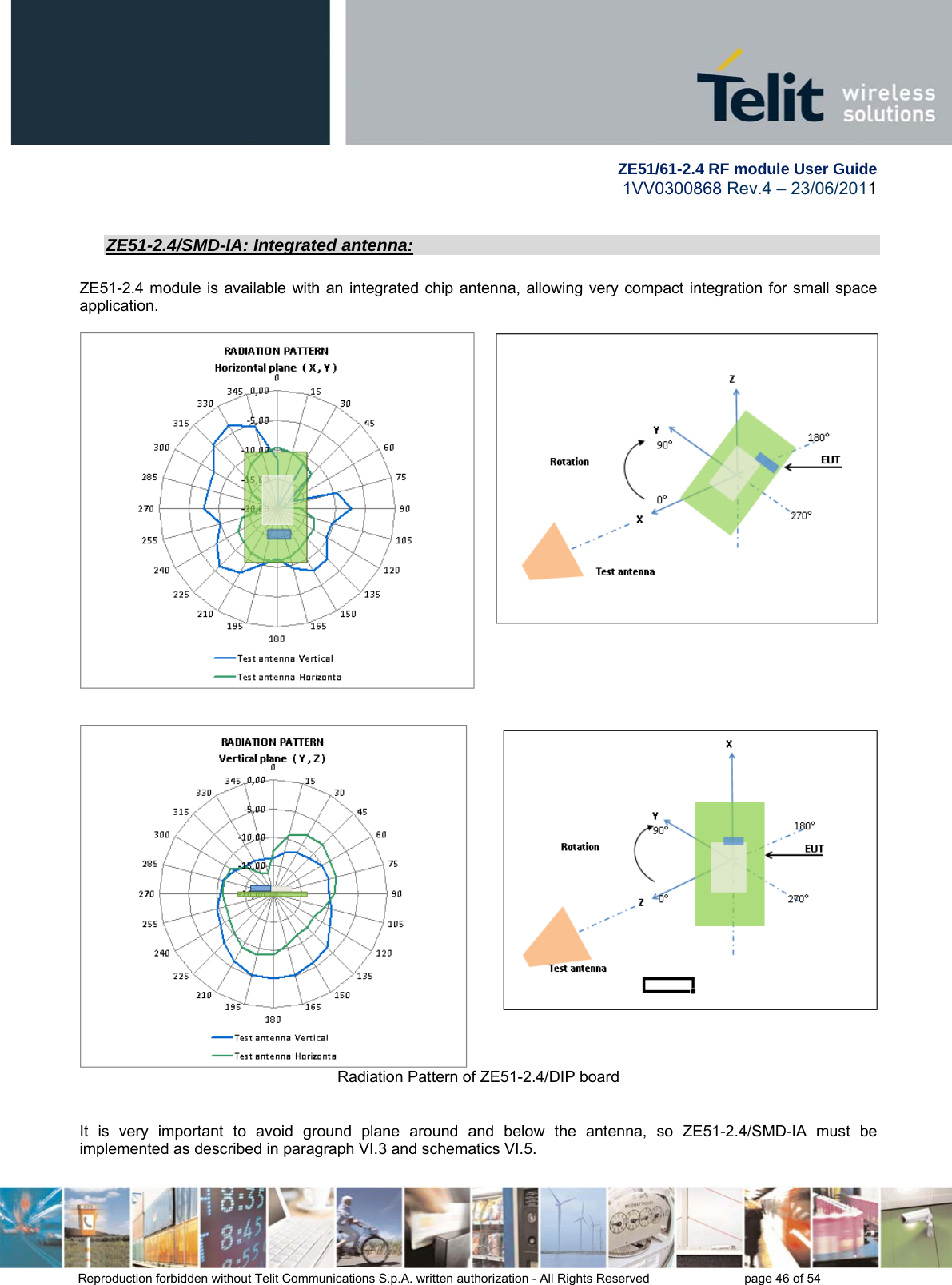
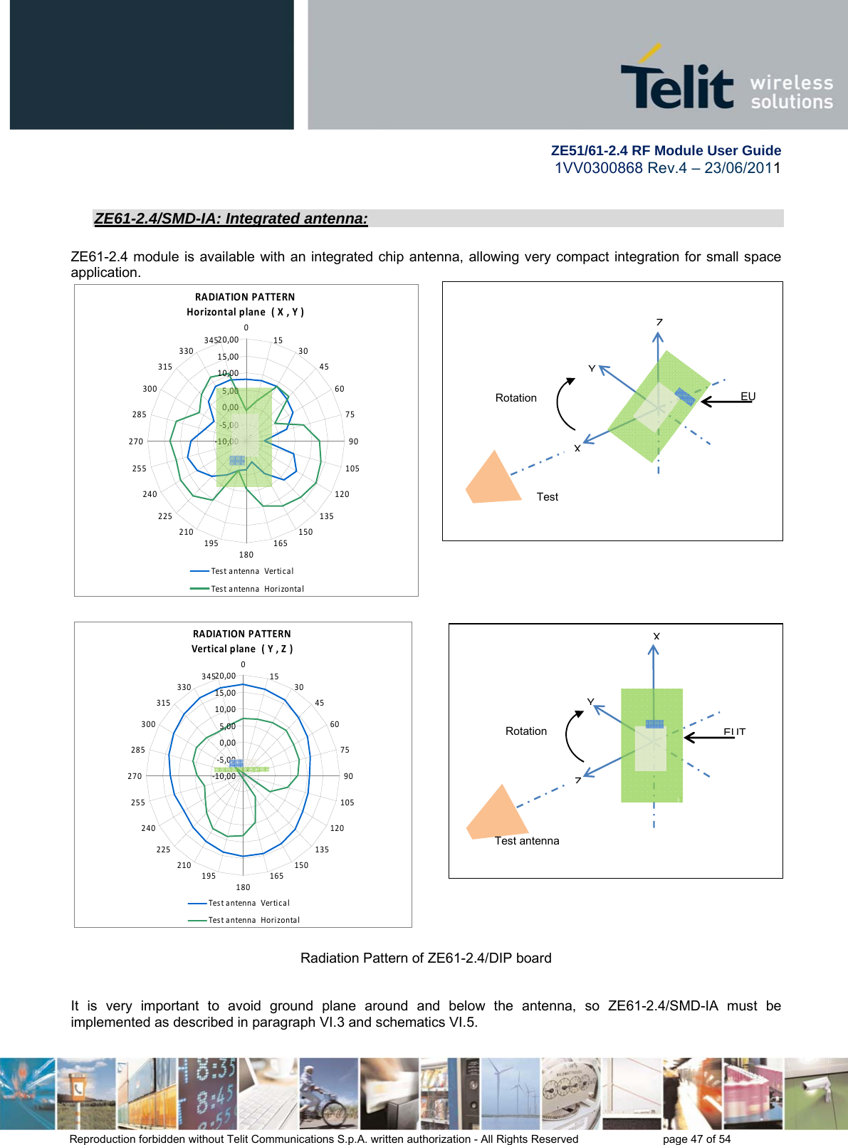
![ZE51/61-2.4 RF Module User Guide 1VV0300868 Rev.4 – 23/06/2011 Reproduction forbidden without Telit Communications S.p.A. written authorization - All Rights Reserved page 7 of 54 I.3. Reference documents [1] IEEE Std. 802.15.4-2006 Wireless MAC and PHY Specifications for Low Rate - WPANs[2] ERC Rec 70-03 ERC Recommendation for SRD, October 2010[3] EN 300 328-1 V1.7.1 (Europe) ETSI Standards for SRD , October 2006[4] EN 300 440-1 V1.6.1 (Europe) ETSI Standards for SRD , August 2010[5] 2002/95/EC Directive of the European Parliament and of the Council, 27 January 2003[6] CFR47 Part 15 (US) FCC Standards for SRD[7] ARIB STD-T66 (Japan) ARIB Standards for SRD[8] Z-One Pro Protocol Stack User Guide 1vv0300902[9] 2006/771/EC Harmonization of the radio spectrum for use by short-range devices[10] 2009/381/EC Amending Decision 2006/771/EC on harmonization of the radio spectrum for use by short-range devices[11] SR Manager Tool User Guide 1vv0300899 [12] ZigBee PRO Democase Getting Started 1vv0300901[13] ZigBee PRO Democase User Guide 1vv0300900I.4. Document change log RReevviissiioonn DDaattee CChhaannggeess ISSUE # 0 11/05/10 First Release ISSUE # 1 28/07/10 Added ZE61-2.4 ISSUE # 2 04/02/11 Updated regulation requirements and schematics in VI.5 ISSUE # 3 14/03/11 Added link for ZE51 USB dongle drivers, info regarding CC debugger. Added in Annex paragraph regarding Conformity Assessment Issues FCC/IC and Declaration of conformity ISSUE # 4 23/05/11 Added text regarding Conformity Assessment Issues FCC/IC and FCC/IC Certification Update of Reference documents, DC characteristics, Functional characteristics, Absolute maximum ratings, DIP module mechanical dimensions and pin-out labels, Correspondence table and Antenna matching Added ZE61-2.4/DIP board radiation pattern](https://usermanual.wiki/Telit-Communications-S-p-A/XE61/User-Guide-1490301-Page-7.png)
![ZE51/61-2.4 RF Module User Guide 1VV0300868 Rev.4 – 23/06/2011 Reproduction forbidden without Telit Communications S.p.A. written authorization - All Rights Reserved page 9 of 54 CHAPTER II. REQUIREMENTS II.1. Regulations requirements The ZE51/61-2.4 module is a [1],[2],[6],[7] compliant multi channel radio modem in the 2.4GHz band (unlicensed frequency band). Europe Regulation: The “ERC recommendation 70-03” [2] describes the limits band in the 2.4GHz license free band, in terms of bandwidth, maximum power, duty cycle, channel spacing and type of application. It gives the following limitations: Class Frequency band Maximum radiated power Channel spacing Duty cycle Notes Annex 1h (Non-Specific Short range Devices) 2400 – 2483.5 MHz 10 mW e.i.r.p. No channel spacing specified No restriction Annex 3a (Wideband Data Transmission systems) 2400 – 2483.5 MHz 100 mW e.i.r.p. and 100 mW/100 kHz e.i.r.p. density applies when frequency hopping modulation is used, 10 mW/MHz e.i.r.p. density applies when other types of modulation are used.(*)(**) No channel spacing specified. No restriction For wide band modulations other than FHSS, the maximum e.i.r.p. density is limited to 10 mW/MHz (*) Compliant to the EU Commission Decision [9], [10]. Techniques to access spectrum and mitigate interference that provide at least equivalent performance to the techniques described in harmonized standards adopted under Directive 1999/5/EC must be used. (**) For IEEE802.15.4 DSSS modulation used by ZigBee, the modulated signal is spread over 2MHz. So, the maximum radiated power is 20mW. The output power must therefore be reduced to approximately +13 dBm in order to get CE approval. The final output power level will depend on the antenna used.](https://usermanual.wiki/Telit-Communications-S-p-A/XE61/User-Guide-1490301-Page-9.png)
![ZE51/61-2.4 RF Module User Guide 1VV0300868 Rev.4 – 23/06/2011 Reproduction forbidden without Telit Communications S.p.A. written authorization - All Rights Reserved page 11 of 54 resources accounting systems or security systems. 2.3. Maximum mean e.i.r.p. density is 10 mW/MHz. Maximum 100 mW e.i.r.p. Indoor applications For the complete document please refer to [2] and EU Commission Decision [9], [10]. The 2.4 Ghz band is a harmonized band in most of Europe. So the product must be declared in compliance with the harmonized ETSI standards EN 300 440 (Class 1h) or EN 300 228 (Class 3a). Finally, the module complies with the new European Directive 2002/95/EC concerning the Restrictive Usage of Hazardous Substances (RoHS). USA Regulation: In the United States the FCC is responsible for the regulation of all RF devices. Our module intended for unlicensed operation is regulated by CFR 47, Part 15 [6]. The 2.4 GHz band used for unlicensed radio equipment is regulated by section 15.247. Japan regulation In Japan the unlicensed use of short range devices in the 2.4 GHz ISM band is regulated by the ARIB standard STD-T66 [7].](https://usermanual.wiki/Telit-Communications-S-p-A/XE61/User-Guide-1490301-Page-11.png)
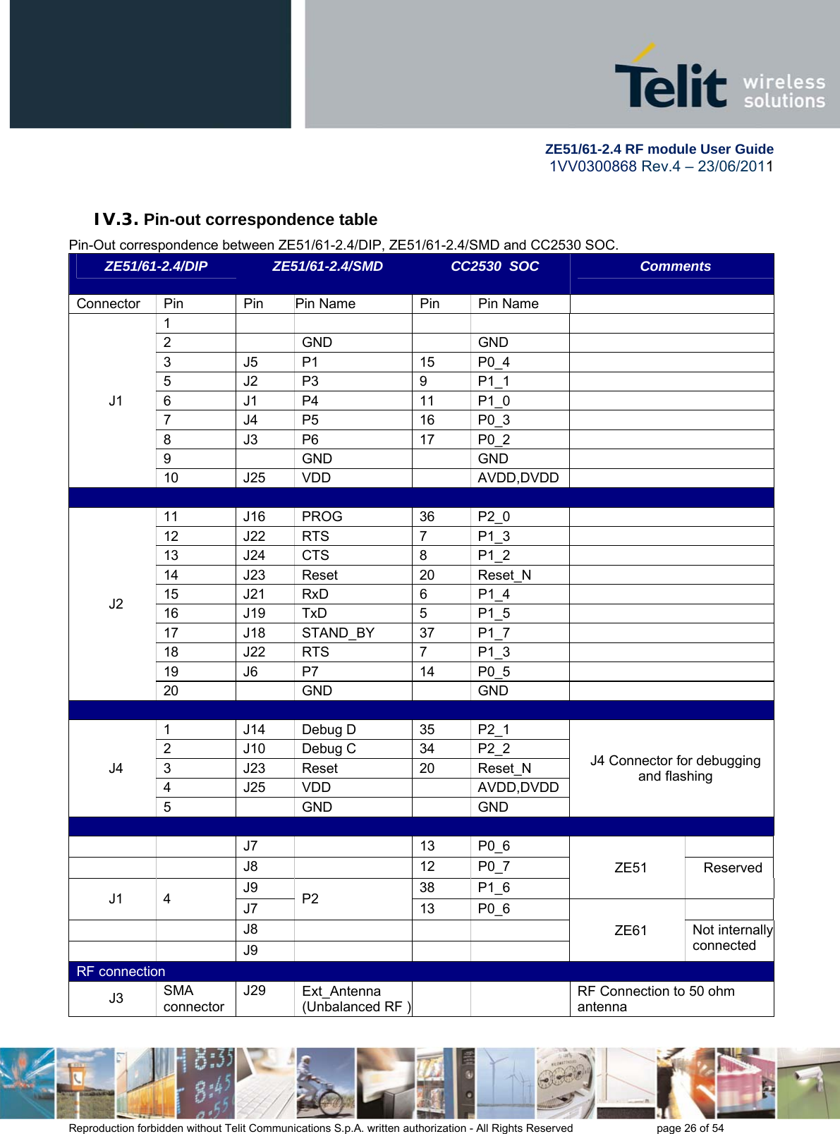
![ZE51/61-2.4 RF module User Guide 1VV0300868 Rev.4 – 23/06/2011 Reproduction forbidden without Telit Communications S.p.A. written authorization - All Rights Reserved page 12 of 54 II.2. Functional Requirements The ZE51/61-2.4 module is a complete solution from serial interface to RF interface. The ZE51/61-2.4 module has a digital part and a RF part. The digital part has the following functionalities: - Communication interface - I/O management - Micro controller with embedded software The RF part has the following functionalities: - 2.4 GHz IEEE 802.15.4 compliant RF transceiver - Half Duplex bi-directional link - RF front-end component with low noise Rx amplification and Tx power amplification (ZE61-2.4 module only) II.3. Software The ZE51/61-2.4 module is provided pre-flashed with Telit in-house ZigBee® PRO stack. Please refer to ZigBee PRO Protocol Stack User Guide [8] for detail information. In case the customer needs to develop his own software, different tools are available: 8051 compiler from IAR : http://www.iar.se/website1/1.0.1.0/244/1/ CC debugger: http://focus.ti.com/docs/toolsw/folders/print/cc-debugger.html The technical support for these tools will be done by the providing company. All necessary drivers for ZE51-2.4 Usb dongle can be found under the following link: http://www.ftdichip.com/Drivers/VCP.htm A complete correspondence table of the connections between the CC2530 and the pin out of the module, as well as the connections to the included STM M24C64 EEPROM can be found in chapter IV.3. In case, the customer wants to test the RF performances of the module, Telit can provide its own proprietary test software that is available in the download zone together with description of all the functionalities.](https://usermanual.wiki/Telit-Communications-S-p-A/XE61/User-Guide-1490301-Page-12.png)
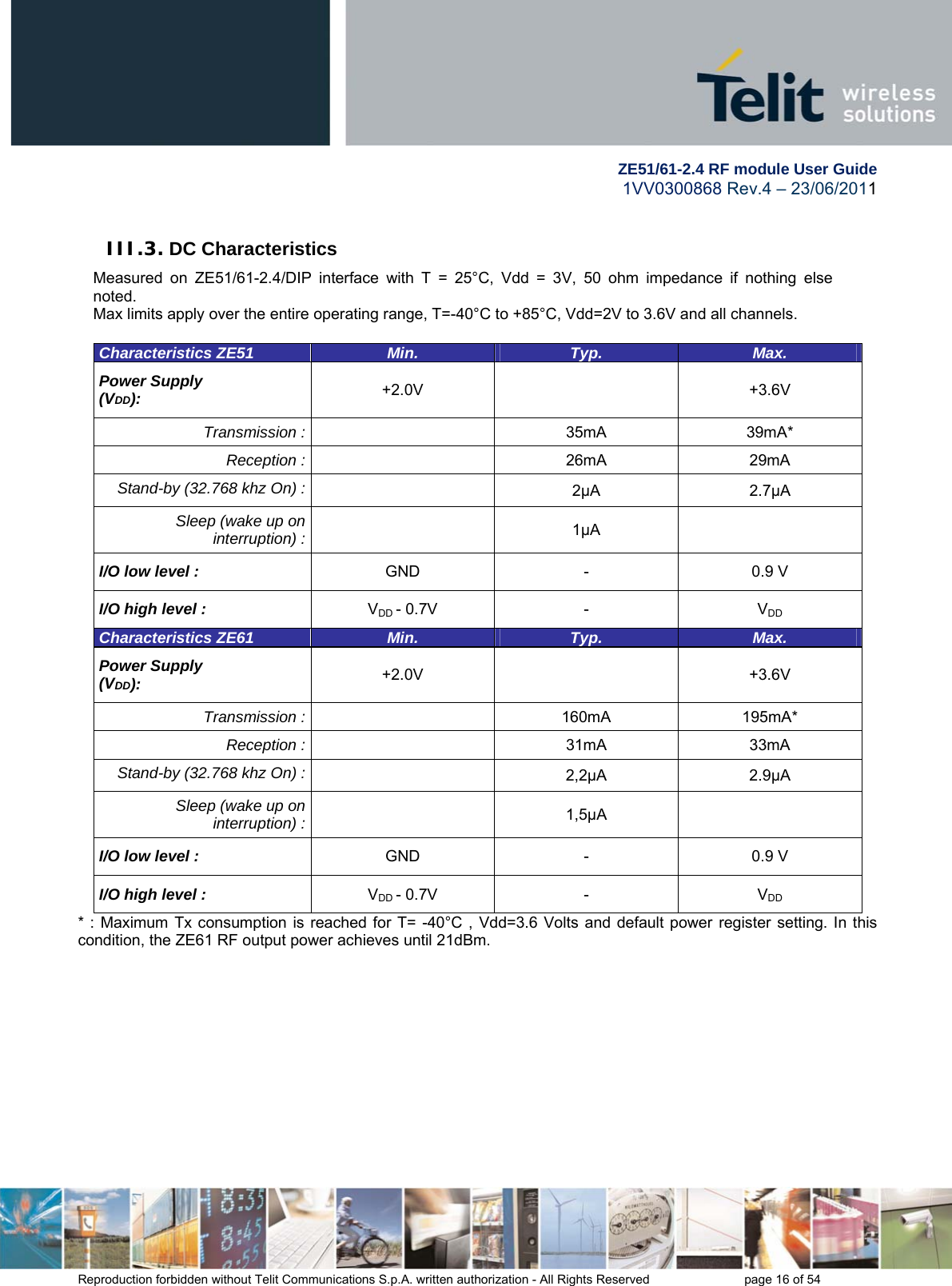
![ZE51/61-2.4 RF Module User Guide 1VV0300868 Rev.4 – 23/06/2011 Reproduction forbidden without Telit Communications S.p.A. written authorization - All Rights Reserved page 17 of 54 III.4. Functional characteristics Measured on ZE51/61-2.4/DIP interface with T = 25°C, Vdd = 3V, 50 ohm impedance if nothing else noted. Global Frequency band 2400 - 2483.5 MHz Channel spacing 5 MHz Channel number 16 : Channel 11 (2405MHz) Channel 26 (2480MHz) Technology DSSS Modulation O-QPSK with half sine pulse shaping Radio bit rate 250 kbps Transmit chip rate 2 Mchip/s Transmission ZE51 Min. Typ. Max. Output Power +4dBm ± 1 dB on the whole band (selectable by software ) Harmonics 2nd harmonic 3rd harmonic -45 dBm -59 dBm Spurious emission 30 - 1000 MHz 1 - 12.75 GHz 1.8 - 1.9 GHz 5.15 - 5.3 GHz -36 dBm -30 dBm -47 dBm -47 dBm (Complies with [3], [4], [6],[7]) Error Vector Magnitude (EVM) 5% 15% Transmission ZE61 Min. Typ. Max.Output Power* +19dBm ± 1 dB on the whole band (selectable by software ) Harmonics 2nd harmonic 3rd harmonic -42 dBm -44 dBm Spurious emission 30 - 1000 MHz 1 - 12.75 GHz 1.8 - 1.9 GHz 5.15 - 5.3 GHz -36 dBm -30 dBm -47 dBm -47 dBm](https://usermanual.wiki/Telit-Communications-S-p-A/XE61/User-Guide-1490301-Page-17.png)
![ZE51/61-2.4 RF module User Guide 1VV0300868 Rev.4 – 23/06/2011 Reproduction forbidden without Telit Communications S.p.A. written authorization - All Rights Reserved page 18 of 54 (Complies with [3], [4], [6], [7]) Error Vector Magnitude (EVM) 5% 15% * : It’s the responsibility of Telit customers to check that RF output power of the final product is compliant with the local regulation. See the table in chapter VIII.5 which shows the typical output power for different power settings. Reception ZE51 Min. Typ. Max. Sensitivity for PER=1% - -96 dBm -97 dBm Saturation for PER=1% - 10 dBm - Adjacent channel rejection +/- 5 MHz channel spacing - 49 dB - Wanted signal @ -82 dBm, adjacent modulated channel @ +/- 5 MHz, for PER = 1 %. Alternate channel rejection +/- 10 MHz channel spacing - 54 dB - Wanted signal @ -82 dBm, adjacent modulated channel @ +/- 10 MHz, for PER = 1 %. Blocking/Desensitisation @ ±5MHz @ ±10MHz @±20MHz @±50MHz - - - - - 40 dBm - 35 dBm - 38 dBm - 37 dBm - - - - Wanted signal 3 dB above the sensitivity level, CW jammer, for PER = 1%. (Measured according to EN 300 440 class 2) Spurious emission in 30 MHz - 12.75 GHz - - -47 dBm (Complies with [3], [4], [6],[7])](https://usermanual.wiki/Telit-Communications-S-p-A/XE61/User-Guide-1490301-Page-18.png)
![ZE51/61-2.4 RF Module User Guide 1VV0300868 Rev.4 – 23/06/2011 Reproduction forbidden without Telit Communications S.p.A. written authorization - All Rights Reserved page 19 of 54 Reception ZE61 Min. Typ. Max. Sensitivity for PER=1% - -99 dBm -100dBm Saturation for PER=1% - 0 dBm - Adjacent channel rejection +/- 5 MHz channel spacing - 49 dB - Wanted signal @ -82 dBm, adjacent modulated channel @ +/- 5 MHz, for PER = 1 %. Alternate channel rejection +/- 10 MHz channel spacing - 54 dB - Wanted signal @ -82 dBm, adjacent modulated channel @ +/- 10 MHz, for PER = 1 %. Blocking/Desensitisation @ ±5MHz @ ±10MHz @±20MHz @±50MHz - - - - - 35 dBm - 35 dBm - 33 dBm - 35 dBm - - - - Wanted signal 3 dB above the sensitivity level, CW jammer, for PER = 1%. (Measured according to EN 300 440 class 2) Spurious emission in 30 MHz - 12.75 GHz - - -47 dBm (Complies with [3], [4], [6],[7])](https://usermanual.wiki/Telit-Communications-S-p-A/XE61/User-Guide-1490301-Page-19.png)