Telit Communications S p A XE61 Wireless module 2.4GHz ZE61/LE61/XE61-2.4 User Manual Revised manual
Telit Communications S.p.A. Wireless module 2.4GHz ZE61/LE61/XE61-2.4 Revised manual
Revised manual

ZE51/61-2.4 RF Module User Guide
1VV0300868 Rev.4 – 23/06/2011

ZE51/61-2.4 RF module User Guide
1VV0300868 Rev.4 – 23/06/2011
Reproduction forbidden without Telit Communications S.p.A. written authorization - All Rights Reserved page 2 of 54
This document is related to the following product :

ZE51/61-2.4 RF Module User Guide
1VV0300868 Rev.4 – 23/06/2011
Reproduction forbidden without Telit Communications S.p.A. written authorization - All Rights Reserved page 3 of 54
DISCLAIMER
The information contained in this document is the proprietary information of Telit Communications S.p.A.
and its affiliates (“TELIT”). The contents are confidential and any disclosure to persons other than the
officers, employees, agents or subcontractors of the owner or licensee of this document, without the prior
written consent of Telit, is strictly prohibited.
Telit makes every effort to ensure the quality of the information it makes available. Notwithstanding the
foregoing, Telit does not make any warranty as to the information contained herein, and does not accept
any liability for any injury, loss or damage of any kind incurred by use of or reliance upon the information.
Telit disclaims any and all responsibility for the application of the devices characterized in this document,
and notes that the application of the device must comply with the safety standards of the applicable
country, and where applicable, with the relevant wiring rules.
Telit reserves the right to make modifications, additions and deletions to this document due to
typographical errors, inaccurate information, or improvements to programs and/or equipment at any time
and without notice. Such changes will, nevertheless be incorporated into new editions of this document.
Copyright: Transmittal, reproduction, dissemination and/or editing of this document as well as utilization
of its contents and communication thereof to others without express authorization are prohibited.
Offenders will be held liable for payment of damages. All rights are reserved.
© Copyright Telit RF Technologies 2011.

ZE51/61-2.4 RF module User Guide
1VV0300868 Rev.4 – 23/06/2011
Reproduction forbidden without Telit Communications S.p.A. written authorization - All Rights Reserved page 4 of 54
CONTENTS
CHAPTER I. INTRODUCTION ................................................................................................................... 6
I.1. AIM OF THE DOCUMENT .................................................................................................................................................................................... 6
I.2. CONTACT INFORMATION, SUPPORT .................................................................................................................................................................. 6
I.3. REFERENCE DOCUMENTS ................................................................................................................................................................................. 7
I.4. DOCUMENT CHANGE LOG ................................................................................................................................................................................. 7
I.5. GLOSSARY ...................................................................................................................................................................................................... 8
CHAPTER II. REQUIREMENTS ................................................................................................................ 9
II.1. REGULATIONS REQUIREMENTS ........................................................................................................................................................................ 9
II.2. FUNCTIONAL REQUIREMENTS........................................................................................................................................................................ 12
II.3. SOFTWARE .................................................................................................................................................................................................. 12
II.4. TEMPERATURE REQUIREMENTS .................................................................................................................................................................... 13
CHAPTER III. GENERAL CHARACTERISTICS ...................................................................................... 14
III.1. MECHANICAL CHARACTERISTICS ................................................................................................................................................................. 14
III.2. MECHANICAL DIMENSIONS ........................................................................................................................................................................... 15
III.3. DC CHARACTERISTICS ................................................................................................................................................................................ 16
III.4. FUNCTIONAL CHARACTERISTICS .................................................................................................................................................................. 17
III.5. DIGITAL CHARACTERISTICS ......................................................................................................................................................................... 20
III.6. ABSOLUTE MAXIMUM RATINGS .................................................................................................................................................................... 21
III.7. ORDERING INFORMATION ............................................................................................................................................................................ 22
CHAPTER IV. TECHNICAL DESCRIPTION ............................................................................................ 23
IV.1. PIN-OUT OF THE SMD MODULE .................................................................................................................................................................... 23
IV.2. DIP MODULE MECHANICAL DIMENSIONS AND PIN-OUT ................................................................................................................................... 25
IV.3. PIN-OUT CORRESPONDENCE TABLE .............................................................................................................................................................. 26
IV.4. DESCRIPTION OF THE SIGNALS ..................................................................................................................................................................... 27
CHAPTER V. PROCESS INFORMATION ............................................................................................... 28
V.1. DELIVERY ..................................................................................................................................................................................................... 28
V.2. STORAGE ..................................................................................................................................................................................................... 29
V.3. SOLDERING PAD PATTERN ............................................................................................................................................................................. 29
V.4. SOLDER PASTE COMPOSITION (ROHS PROCESS) ........................................................................................................................................... 31
V.5. PLACEMENT .................................................................................................................................................................................................. 31
V.6. SOLDERING PROFILE (ROHS PROCESS) ......................................................................................................................................................... 32
CHAPTER VI. BOARD MOUNTING RECOMMENDATION ..................................................................... 34
VI.1. ELECTRICAL ENVIRONMENT .......................................................................................................................................................................... 34

ZE51/61-2.4 RF Module User Guide
1VV0300868 Rev.4 – 23/06/2011
Reproduction forbidden without Telit Communications S.p.A. written authorization - All Rights Reserved page 5 of 54
VI.2. POWER SUPPLY DECOUPLING ON ZE51/61-2.4 MODULE ............................................................................................................................... 35
VI.3. RF LAYOUT CONSIDERATIONS ...................................................................................................................................................................... 36
VI.4. ANTENNA CONNECTION ON PRINTED CIRCUIT BOARDS ................................................................................................................................. 37
VI.5. ZE51/61-2.4 INTERFACING : ........................................................................................................................................................................ 38
CHAPTER VII. ANTENNA CONSIDERATIONS....................................................................................... 41
VII.1. ANTENNA RECOMMENDATIONS ................................................................................................................................................................... 41
VII.2. ANTENNA MATCHING .................................................................................................................................................................................. 42
VII.3. ANTENNA TYPES ........................................................................................................................................................................................ 43
VII.4. EXTERNAL ANTENNA .................................................................................................................................................................................. 43
VII.5. EMBEDDABLE ANTENNAS ............................................................................................................................................................................ 45
CHAPTER VIII. ANNEXES ....................................................................................................................... 48
VIII.1. DECLARATION OF CONFORMITY ................................................................................................................................................................ 48
VIII.2. CONFORMITY ASSESSMENT ISSUES FCC/IC.............................................................................................................................................. 52
VIII.3. EXAMPLES OF PROPAGATION ATTENUATION ............................................................................................................................................... 53
VIII.4. OUTPUT POWER PROGRAMMING................................................................................................................................................................ 54

ZE51/61-2.4 RF module User Guide
1VV0300868 Rev.4 – 23/06/2011
Reproduction forbidden without Telit Communications S.p.A. written authorization - All Rights Reserved page 6 of 54
CHAPTER I. INTRODUCTION
I.1. Aim of the Document
The aim of this document is to present the features and the application of the ZE51/61-2.4 radio module. After the
introduction, the characteristics of the ZE51/61-2.4 radio module will be described within the following distinct
chapters:
- Requirements
- General Characteristics
- Technical description
- Process information
- Board Mounting Recommendations
- Antenna Considerations
I.2. Contact Information, Support
For general contact, technical support, to report documentation errors and to order manuals, contact Telit Technical
Support Center (TTSC) at:
TS-SRD@telit.com
TS-NORTHAMERICA@telit.com
TS-LATINAMERICA@telit.com
TS-APAC@telit.com
Alternatively, use:
http://www.telit.com/en/products/technical-support-center/contact.php
For detailed information about where you can buy the Telit modules or for recommendations on accessories and
components visit:
http://www.telit.com
To register for product news and announcements or for product questions contact Telit Technical Support Center
(TTSC).
Our aim is to make this guide as helpful as possible. Keep us informed of your comments and suggestions for
improvements. Telit appreciates feedback from the users of our information.
ZE51/61-2.4 RF Module User Guide
1VV0300868 Rev.4 – 23/06/2011
Reproduction forbidden without Telit Communications S.p.A. written authorization - All Rights Reserved page 7 of 54
I.3. Reference documents
[1] IEEE Std. 802.15.4-2006 Wireless MAC and PHY Specifications for Low Rate - WPANs
[2] ERC Rec 70-03 ERC Recommendation for SRD, October 2010
[3] EN 300 328-1 V1.7.1 (Europe) ETSI Standards for SRD , October 2006
[4] EN 300 440-1 V1.6.1 (Europe) ETSI Standards for SRD , August 2010
[5] 2002/95/EC Directive of the European Parliament and of the Council, 27 January
2003
[6] CFR47 Part 15 (US) FCC Standards for SRD
[7] ARIB STD-T66 (Japan) ARIB Standards for SRD
[8] Z-One Pro Protocol Stack User
Guide
1vv0300902
[9] 2006/771/EC Harmonization of the radio spectrum for use by short-range devices
[10] 2009/381/EC Amending Decision 2006/771/EC on harmonization of the radio
spectrum for use by short-range devices
[11] SR Manager Tool User Guide 1vv0300899
[12] ZigBee PRO Democase Getting
Started 1vv0300901
[13] ZigBee PRO Democase Use
r
Guide 1vv0300900
I.4. Document change log
R
Re
ev
vi
is
si
io
on
n
D
Da
at
te
e
C
Ch
ha
an
n
g
ge
es
s
ISSUE # 0 11/05/10 First Release
ISSUE # 1 28/07/10 Added ZE61-2.4
ISSUE # 2 04/02/11 Updated regulation requirements and schematics in VI.5
ISSUE # 3 14/03/11 Added link for ZE51 USB dongle drivers, info regarding CC debugger.
Added in Annex paragraph regarding Conformity Assessment Issues
FCC/IC and Declaration of conformity
ISSUE # 4 23/05/11 Added text regarding Conformity Assessment Issues FCC/IC and
FCC/IC Certification
Update of Reference documents, DC characteristics, Functional
characteristics, Absolute maximum ratings, DIP module mechanical
dimensions and pin-out labels, Correspondence table and Antenna
matching
A
dded ZE61-2.4/DIP board radiation pattern

ZE51/61-2.4 RF module User Guide
1VV0300868 Rev.4 – 23/06/2011
Reproduction forbidden without Telit Communications S.p.A. written authorization - All Rights Reserved page 8 of 54
I.5. Glossary
ARIB Association of Radio Industries and Businesses
BER Bit Error Rate
Bits/s Bits per second
(
1000 bits/s = 1Kbps = 1Kbaud
)
CEPT European Conference of Postal and Telecommunications Administrations
CFR Code of Federal Regulations
Chips Chip or chip sequence refers to a spreading-code used to transform the original
data to DSSS
CW Continuous Wave
dBm Power level in decibel milliwatt
(
10 lo
g
(
P/1mW
))
DSSS Direct Sequence Spread Spectrum
EIRP Effective Isotropic Radiated Power
EMC Electro Ma
g
netic Compatibilit
y
EPROM Electrical Programmable Read Only Memory
ERC European Radiocommunications Committee
ETR ETSI Technical Report
ETSI European Telecommunication Standard Institute
FCC Federal Communications Commission
IEEE Institute of Electrical and Electronics Engineers
ISM Industrial, Scientific and Medical
KB 1024 bytes (1 byte = 8 bits)
K
bps kilobits/s
LBT Listen Before Talk
LNA Low Noise Amplifier
MAC Medium Access Control
MHz Mega Hertz (1 MHz = 1000 kHz)
Mchip/s Mega chips per second (A measure of the speed with which chips are generated
in DSSS)
PCB Printed Circuit Board
PROM Programmable Read Only Memory
PER Packet Error Rate
PHY Physical Layer
NRZ Non return to Zero
RF Radio Frequency
RoHS Restriction of Hazardous Substances
RSSI Receive Strength Signal Indicator
Rx Reception
SRAM Static Random Access Memory
SRD Short Range Device
SMD Surface Mounted Device
Tx Transmission
V
ia Metal Hole on a printed circuit board
WPANs Wireless Personal Area Networks
ZE51/61-2.4 RF Module User Guide
1VV0300868 Rev.4 – 23/06/2011
Reproduction forbidden without Telit Communications S.p.A. written authorization - All Rights Reserved page 9 of 54
CHAPTER II. REQUIREMENTS
II.1. Regulations requirements
The ZE51/61-2.4 module is a [1],[2],[6],[7] compliant multi channel radio modem in the 2.4GHz band (unlicensed
frequency band).
Europe Regulation:
The “ERC recommendation 70-03” [2] describes the limits band in the 2.4GHz license free band, in terms of bandwidth,
maximum power, duty cycle, channel spacing and type of application. It gives the following limitations:
Class Frequency
band Maximum radiated power Channel
spacing Duty cycle Notes
Annex 1h
(Non-Specific
Short range
Devices)
2400 – 2483.5
MHz 10 mW e.i.r.p.
No channel
spacing
specified
No
restriction
Annex 3a
(Wideband Data
Transmission
systems)
2400 – 2483.5
MHz
100 mW e.i.r.p. and 100
mW/100 kHz e.i.r.p. density
applies when frequency
hopping modulation is used,
10 mW/MHz e.i.r.p. density
applies when other types of
modulation are used.(*)(**)
No channel
spacing
specified.
No
restriction
For wide band
modulations other than
FHSS, the maximum
e.i.r.p. density is limited
to 10 mW/MHz
(*) Compliant to the EU Commission Decision [9], [10]. Techniques to access spectrum and mitigate interference
that provide at least equivalent performance to the techniques described in harmonized standards adopted under
Directive 1999/5/EC must be used.
(**) For IEEE802.15.4 DSSS modulation used by ZigBee, the modulated signal is spread over 2MHz. So, the
maximum radiated power is 20mW. The output power must therefore be reduced to approximately +13 dBm in
order to get CE approval. The final output power level will depend on the antenna used.

ZE51/61-2.4 RF module User Guide
1VV0300868 Rev.4 – 23/06/2011
Reproduction forbidden without Telit Communications S.p.A. written authorization - All Rights Reserved page 10 of 54
Restrictions for non specific SR devices Annex 1h 2400-2483.5MHz:
Country Restriction Reason/Remark
Norway Implemented
This subsection does not apply for the
geographical area within a radius of 20 km
from the centre of N
y
-Ålesund
Russian
Federation Bluetooth
Ukraine Limited implementation e.i.r.p. ≤100 mW
Restrictions for Wideband Data Transmission systems Annex 3a 2400-2483.5MHz:
Country Restriction Reason/Remark
France
Outdoor use limited to 10
mW e.i.r.p. within the
band 2454-2483.5 MHz
Military Radiolocation use. Reforming of
the 2.4 GHz band has been ongoing in
recent years to allow current relaxed
regulation. Full implementation planned
2012
Italy
For private use, a general authorisation is
required if WAS/RLAN’s are used outside
own premises. For public use, a general
authorization is required
Ukraine Limited Implemented
e.i.r.p. ≤100 mW with built-in antenna with
amplification factor up to 6 dBi
Norway Implemented
This subsection does not apply for the
geographical area within a radius of 20 km
from the centre of Ny-Ålesund
Russian
Federation
1. SRD with FHSS modulation
1.1. Maximum 2.5 mW e.i.r.p.
1.2. Maximum 100 mW e.i.r.p. Permitted for
use SRD for outdoor applications without
restriction on installation height only for
purposes of gathering telemetry information for
automated monitoring and resources
accounting systems.
Permitted to use SRD for other purposes for
outdoor applications only when the installation
height is not exceeding 10 m above the ground
surface.
1.3.Maximum 100 mW e.i.r.p. Indoor
applications
2. SRD with DSSS and other than FHSS
wideband modulation
2.1. Maximum mean e.i.r.p. density is 2
mW/MHz. Maximum 100 mW e.i.r.p.
2.2. Maximum mean e.i.r.p. density is 20
mW/MHz. Maximum 100 mW e.i.r.p. Permitted
to use SRD for outdoor applications
only for purposes of gathering telemetry
information for automated monitoring and

ZE51/61-2.4 RF Module User Guide
1VV0300868 Rev.4 – 23/06/2011
Reproduction forbidden without Telit Communications S.p.A. written authorization - All Rights Reserved page 11 of 54
resources accounting systems or
security systems.
2.3. Maximum mean e.i.r.p. density is 10
mW/MHz. Maximum
100 mW e.i.r.p. Indoor applications
For the complete document please refer to [2] and EU Commission Decision [9], [10].
The 2.4 Ghz band is a harmonized band in most of Europe. So the product must be declared in compliance with
the harmonized ETSI standards EN 300 440 (Class 1h) or EN 300 228 (Class 3a).
Finally, the module complies with the new European Directive 2002/95/EC concerning the Restrictive Usage of
Hazardous Substances (RoHS).
USA Regulation:
In the United States the FCC is responsible for the regulation of all RF devices. Our module intended for
unlicensed operation is regulated by CFR 47, Part 15 [6].
The 2.4 GHz band used for unlicensed radio equipment is regulated by section 15.247.
Japan regulation
In Japan the unlicensed use of short range devices in the 2.4 GHz ISM band is regulated by the ARIB standard
STD-T66 [7].

ZE51/61-2.4 RF module User Guide
1VV0300868 Rev.4 – 23/06/2011
Reproduction forbidden without Telit Communications S.p.A. written authorization - All Rights Reserved page 12 of 54
II.2. Functional Requirements
The ZE51/61-2.4 module is a complete solution from serial interface to RF interface. The ZE51/61-2.4 module has
a digital part and a RF part.
The digital part has the following functionalities:
- Communication interface
- I/O management
- Micro controller with embedded software
The RF part has the following functionalities:
- 2.4 GHz IEEE 802.15.4 compliant RF transceiver
- Half Duplex bi-directional link
- RF front-end component with low noise Rx amplification and Tx power amplification (ZE61-2.4 module
only)
II.3. Software
The ZE51/61-2.4 module is provided pre-flashed with Telit in-house ZigBee® PRO stack. Please refer to ZigBee
PRO Protocol Stack User Guide [8] for detail information.
In case the customer needs to develop his own software, different tools are available:
8051 compiler from IAR : http://www.iar.se/website1/1.0.1.0/244/1/
CC debugger: http://focus.ti.com/docs/toolsw/folders/print/cc-debugger.html
The technical support for these tools will be done by the providing company.
All necessary drivers for ZE51-2.4 Usb dongle can be found under the following link:
http://www.ftdichip.com/Drivers/VCP.htm
A complete correspondence table of the connections between the CC2530 and the pin out of the module, as well
as the connections to the included STM M24C64 EEPROM can be found in chapter IV.3.
In case, the customer wants to test the RF performances of the module, Telit can provide its own
proprietary test software that is available in the download zone together with description of all the
functionalities.
ZE51/61-2.4 RF Module User Guide
1VV0300868 Rev.4 – 23/06/2011
Reproduction forbidden without Telit Communications S.p.A. written authorization - All Rights Reserved page 13 of 54
II.4. Temperature Requirements
Minimum Typical Maximum Unit
Operating
Temperature - 40 25 + 85 °C
Relative humidity @ 25°C 20 75 %
Storage
Temperature - 40 25 + 85 °C

ZE51/61-2.4 RF module User Guide
1VV0300868 Rev.4 – 23/06/2011
Reproduction forbidden without Telit Communications S.p.A. written authorization - All Rights Reserved page 14 of 54
CHAPTER III. GENERAL CHARACTERISTICS
III.1. Mechanical Characteristics
Size : Rectangular 26 x 15 mm
Height : 3 mm
Weight : 1,7 g
PCB thickness: 0.8 mm
Cover : Dimensions : 21 x 14 x 2.2mm
Thickness : 200µm
Components : All SMD components, on one side of the PCB.
Connectors : The terminals allowing conveying I/O signals are half-moons located around.
Mounting : SMD
Half moons on the 4 external sides
Number of pins : 30
ZE51/61-2.4 RF Module User Guide
1VV0300868 Rev.4 – 23/06/2011
Reproduction forbidden without Telit Communications S.p.A. written authorization - All Rights Reserved page 15 of 54
III.2. Mechanical dimensions
ZE51/61-2.4 RF module User Guide
1VV0300868 Rev.4 – 23/06/2011
Reproduction forbidden without Telit Communications S.p.A. written authorization - All Rights Reserved page 16 of 54
III.3. DC Characteristics
Measured on ZE51/61-2.4/DIP interface with T = 25°C, Vdd = 3V, 50 ohm impedance if nothing else
noted.
Max limits apply over the entire operating range, T=-40°C to +85°C, Vdd=2V to 3.6V and all channels.
Characteristics ZE51 Min. Typ. Max.
Power Supply
(VDD): +2.0V +3.6V
Transmission : 35mA 39mA*
Reception : 26mA 29mA
Stand-by (32.768 khz On) : 2µA 2.7µA
Sleep (wake up on
interruption) : 1µA
I/O low level : GND - 0.9 V
I/O high level : VDD - 0.7V - VDD
Characteristics ZE61 Min. Typ. Max.
Power Supply
(VDD): +2.0V +3.6V
Transmission : 160mA 195mA*
Reception : 31mA 33mA
Stand-by (32.768 khz On) : 2,2µA 2.9µA
Sleep (wake up on
interruption) : 1,5µA
I/O low level : GND - 0.9 V
I/O high level : VDD - 0.7V - VDD
* : Maximum Tx consumption is reached for T= -40°C , Vdd=3.6 Volts and default power register setting. In this
condition, the ZE61 RF output power achieves until 21dBm.
ZE51/61-2.4 RF Module User Guide
1VV0300868 Rev.4 – 23/06/2011
Reproduction forbidden without Telit Communications S.p.A. written authorization - All Rights Reserved page 17 of 54
III.4. Functional characteristics
Measured on ZE51/61-2.4/DIP interface with T = 25°C, Vdd = 3V, 50 ohm impedance if nothing else noted.
Global
Frequency band 2400 - 2483.5 MHz
Channel spacing 5 MHz
Channel number 16 : Channel 11 (2405MHz) Channel 26 (2480MHz)
Technology DSSS
Modulation O-QPSK with half sine pulse shaping
Radio bit rate 250 kbps
Transmit chip rate 2 Mchip/s
Transmission ZE51 Min. Typ. Max.
Output Power +4dBm ± 1 dB on the whole band
(selectable by software )
Harmonics
2nd harmonic
3
rd harmonic
-45 dBm
-59 dBm
Spurious emission
30 - 1000 MHz
1 - 12.75 GHz
1.8 - 1.9 GHz
5.15 - 5.3 GHz
-36 dBm
-30 dBm
-47 dBm
-47 dBm
(Complies with [3], [4],
[6],[7])
Error Vector Magnitude
(EVM) 5% 15%
Transmission ZE61 Min. T
y
p. Max.
Output Power* +19dBm ± 1 dB on the whole band
(selectable by software )
Harmonics
2nd harmonic
3
rd harmonic
-42 dBm
-44 dBm
Spurious emission
30 - 1000 MHz
1 - 12.75 GHz
1.8 - 1.9 GHz
5.15 - 5.3 GHz
-36 dBm
-30 dBm
-47 dBm
-47 dBm
ZE51/61-2.4 RF module User Guide
1VV0300868 Rev.4 – 23/06/2011
Reproduction forbidden without Telit Communications S.p.A. written authorization - All Rights Reserved page 18 of 54
(Complies with [3], [4],
[6], [7])
Error Vector Magnitude
(EVM) 5% 15%
* : It’s the responsibility of Telit customers to check that RF output power of the final product is compliant with the
local regulation. See the table in chapter VIII.5 which shows the typical output power for different power settings.
Reception ZE51 Min. Typ. Max.
Sensitivity for PER=1% - -96 dBm -97 dBm
Saturation for PER=1% - 10 dBm -
Adjacent channel
rejection +/- 5 MHz
channel spacing
- 49 dB -
Wanted signal @ -82 dBm, adjacent modulated channel @ +/- 5 MHz,
for PER = 1 %.
Alternate channel
rejection +/- 10 MHz
channel spacing
- 54 dB -
Wanted signal @ -82 dBm, adjacent modulated channel @ +/- 10 MHz,
for PER = 1 %.
Blocking/Desensitisation
@ ±5MHz
@ ±10MHz
@±20MHz
@±50MHz
-
-
-
-
- 40 dBm
- 35 dBm
- 38 dBm
- 37 dBm
-
-
-
-
Wanted signal 3 dB above the sensitivity level, CW jammer,
for PER = 1%.
(Measured according to EN 300 440 class 2)
Spurious emission
in 30 MHz - 12.75 GHz - - -47 dBm
(Complies with [3], [4],
[6],[7])
ZE51/61-2.4 RF Module User Guide
1VV0300868 Rev.4 – 23/06/2011
Reproduction forbidden without Telit Communications S.p.A. written authorization - All Rights Reserved page 19 of 54
Reception ZE61 Min. Typ. Max.
Sensitivity for PER=1% - -99 dBm -100dBm
Saturation for PER=1% - 0 dBm -
Adjacent channel
rejection +/- 5 MHz
channel spacing
- 49 dB -
Wanted signal @ -82 dBm, adjacent modulated channel @ +/- 5 MHz,
for PER = 1 %.
Alternate channel
rejection +/- 10 MHz
channel spacing
- 54 dB -
Wanted signal @ -82 dBm, adjacent modulated channel @ +/- 10 MHz,
for PER = 1 %.
Blocking/Desensitisation
@ ±5MHz
@ ±10MHz
@±20MHz
@±50MHz
-
-
-
-
- 35 dBm
- 35 dBm
- 33 dBm
- 35 dBm
-
-
-
-
Wanted signal 3 dB above the sensitivity level, CW jammer,
for PER = 1%.
(Measured according to EN 300 440 class 2)
Spurious emission
in 30 MHz - 12.75 GHz - - -47 dBm
(Complies with [3], [4],
[6],[7])

ZE51/61-2.4 RF module User Guide
1VV0300868 Rev.4 – 23/06/2011
Reproduction forbidden without Telit Communications S.p.A. written authorization - All Rights Reserved page 20 of 54
III.5. Digital Characteristics
Microcontroller 8051 core
Microcontroller
Memory 256KB Flash, 8KB SRAM,
Peripheral memory 8 KB EEPROM
Serial link* Managed by application.
Full Duplex, from 1200 to 115200 bps
7 or 8 bits, with or without parity, 1 or 2 stop bits
Protocol Type : RS-232, TTL level
Flow control* Managed by application.
None, Software (Xon/Xoff) or Hardware (RTS/CTS)
Other Ultra low power voltage detector and µC supervisory circuit
Specific signals Serial : Tx, Rx, RTS, CTS
Inputs : Reset, Stand-By, Prog
I/O : 7 I/O (among those 5 analog inputs with 7 to 12 bits resolution)
Flashing Through serial
Through the air : DOTA (Download Over The Air) functionality
Embedded
functionality
Point-to-point stack for test purpose available in download zone
ZigBee Pro stack from Telit
*: In ZigBee Democase : 115.200 bps,8 bits, without parity, 1 stop bit, No flow control
ZE51/61-2.4 RF Module User Guide
1VV0300868 Rev.4 – 23/06/2011
Reproduction forbidden without Telit Communications S.p.A. written authorization - All Rights Reserved page 21 of 54
III.6. Absolute Maximum Ratings
ZE51
Voltage applied to VDD -0.3V to +3.9V
Voltage applied to any digital pin -0.3V to VDD+0.3V, max 3.9 V
Input RF level 10 dBm
ZE61
Voltage applied to VDD -0.3V to +3.6V
Voltage applied to any digital pin -0.3V to VDD+0.3V, max 3.6 V
Input RF level 0 dBm
CAUTION
It must be noted that due to some components, ZE51/ZE61 module is
an ESD sensitive device. Therefore, ESD handling precautions should
be carefully observed.
ZE51/61-2.4 RF module User Guide
1VV0300868 Rev.4 – 23/06/2011
Reproduction forbidden without Telit Communications S.p.A. written authorization - All Rights Reserved page 22 of 54
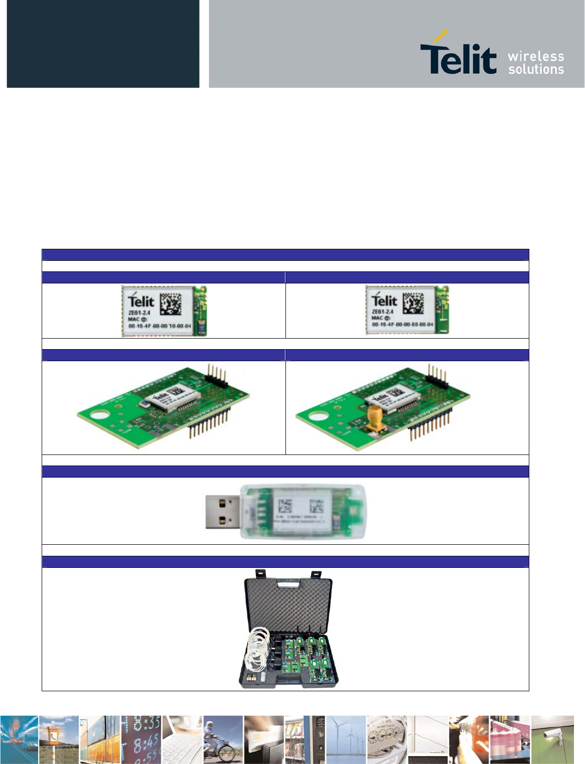
III.7. Ordering information
The following equipments can be ordered:
- The SMD version
- The DIP interface version
- The USB dongle
- The Demo Case
The versions below are considered standard and should be readily available. For other versions, please contact
Telit. Please make sure to give the complete part number when ordering.
Equipment and Part Number
SMD Version
ZE51
/
61-2.4/SMD-IA (With Integrated Antenna) ZE51
/
61-2.4/SMD-WA (Without Integrated Antenna)
DIP Version
ZE51
/
61-2.4/DIP-I
A
(With Integrated Antenna) ZE51
/
61-2.4/DIP-WA (Without Integrated Antenna)
USB Dongle
M ZE51
/
USB
Demo Case
D ZE51
/
61 DEMO
ZE51/61-2.4 RF Module User Guide
1VV0300868 Rev.4 – 23/06/2011
Reproduction forbidden without Telit Communications S.p.A. written authorization - All Rights Reserved page 23 of 54
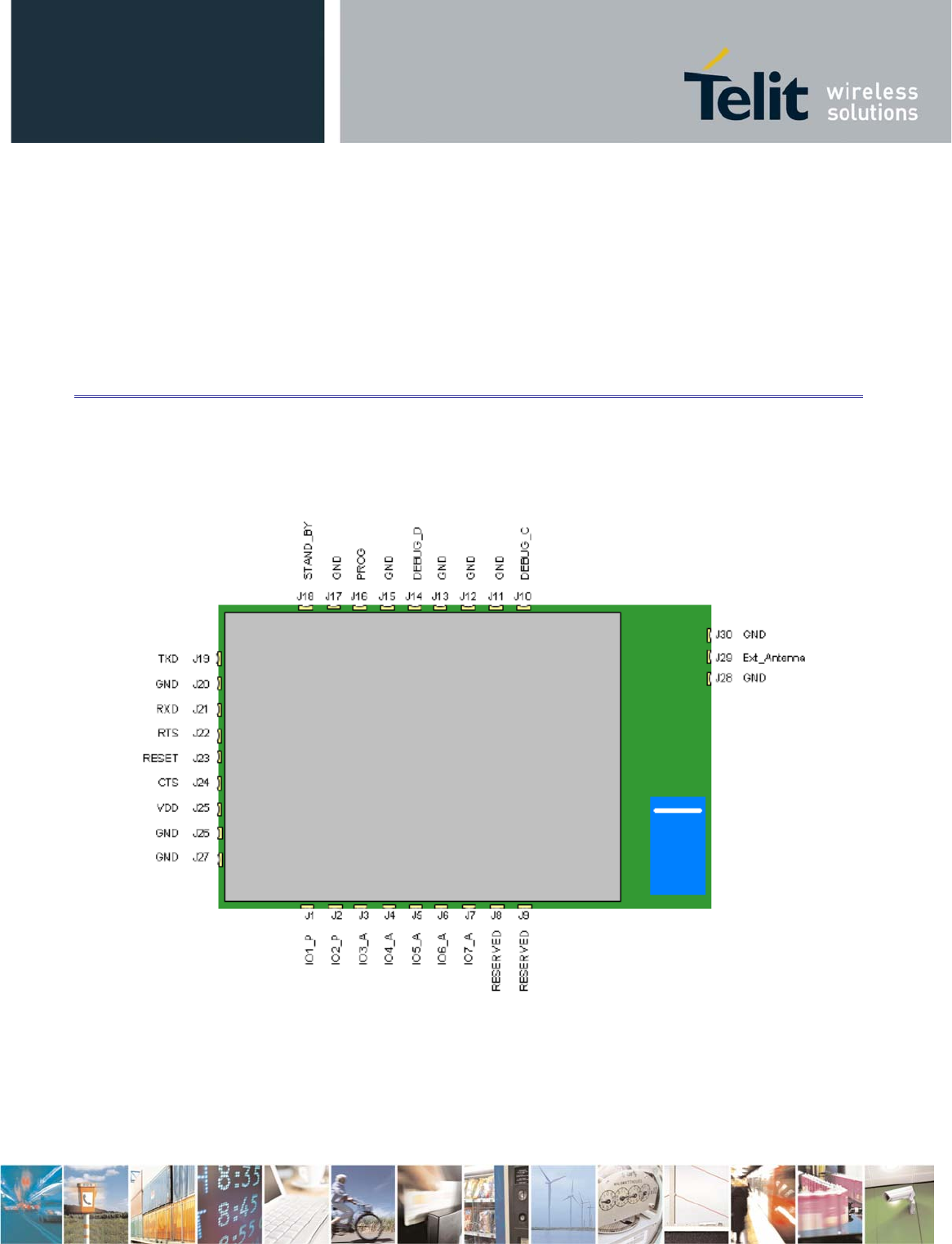
CHAPTER IV. TECHNICAL DESCRIPTION
IV.1. Pin-out of the SMD Module
ZE51/61-2.4 RF module User Guide
1VV0300868 Rev.4 – 23/06/2011
Reproduction forbidden without Telit Communications S.p.A. written authorization - All Rights Reserved page 24 of 54
Pin Pin name Pin type Signal level Function
J30 GND Gnd RF Ground connection for external antenna
J29 Ext_Antenna RF RF I/O connection to external antenna
J28 GND Gnd RF Ground connection for external antenna
J27 GND Gnd Ground
J26 GND Gnd Ground
J25 VDD Power Digital and Radio part power supply pin
J24 CTS I TTL Clear To Send
J23 RESET I TTL µC reset ( Active low with internal pull-up )
J22 RTS O TTL Request To Send
J21 RXD I TTL RxD UART – Serial Data Reception
J20 GND Gnd Ground
J19 TXD O TTL TxD UART – Serial Data Transmission
J18 STAND_BY I TTL Standby ( Active high with internal pull-down )
J17 GND Gnd Ground
J16 PROG I TTL Signal for serial µC flashing ( Active high with internal
pull-down )
J15 GND Gnd Ground
J14 DEBUG_D I/O TTL Debug data.
J13 GND Gnd Ground
J12 GND Gnd Ground
J11 GND Gnd Ground
J10 DEBUG_C I/O TTL Debug clock
J9 RESERVED - - -
J8 RESERVED - - -
J7 IO7_A I/O analog ADC - Analog Input N°7 (Digital I/O capability)
J6 IO6_A I/O analog ADC - Analog Input N°6 (Digital I/O capability)
J5 IO5_A I/O analog ADC - Analog Input N°5 (Digital I/O capability)
J4 IO4_A I/O analog ADC - Analog Input N°4 (Digital I/O capability)
J3 IO3_A I/O analog ADC - Analog Input N°3 (Digital I/O capability)
J2 IO2_P I/O TTL Digital I/O N°2 with 20mA sink/source capability
J1 IO1_P I/O TTL Digital I/O N°1 with 20mA sink/source capability
NOTE: reserved pins must not be connected
ZE51/61-2.4 RF Module User Guide
1VV0300868 Rev.4 – 23/06/2011
Reproduction forbidden without Telit Communications S.p.A. written authorization - All Rights Reserved page 25 of 54
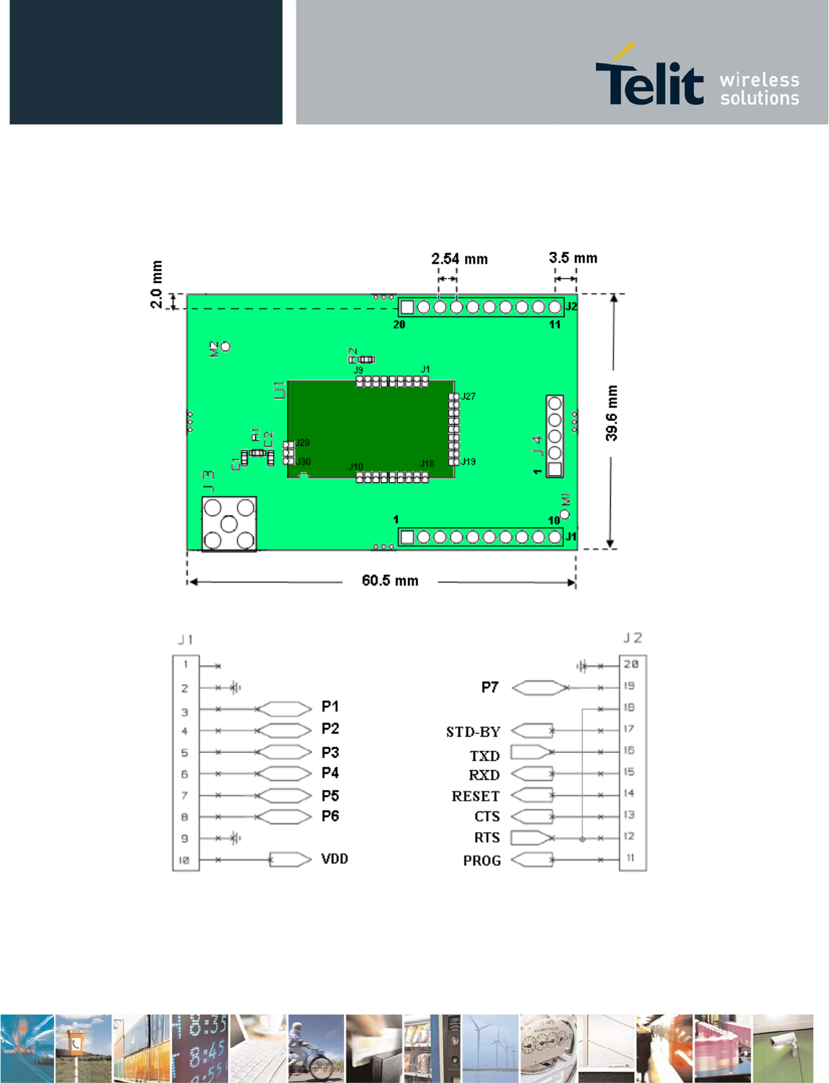
IV.2. DIP Module mechanical dimensions and pin-out
ZE51/61-2.4 RF module User Guide
1VV0300868 Rev.4 – 23/06/2011
Reproduction forbidden without Telit Communications S.p.A. written authorization - All Rights Reserved page 26 of 54
IV.3. Pin-out correspondence table
Pin-Out correspondence between ZE51/61-2.4/DIP, ZE51/61-2.4/SMD and CC2530 SOC.
ZE51/61-2.4/DIP ZE51/61-2.4/SMD
CC2530 SOC
Comments
Connector Pin Pin Pin Name Pin Pin Name
J1
1
2 GND GND
3 J5 P1 15 P0_4
5 J2 P3 9 P1_1
6 J1 P4 11 P1_0
7 J4 P5 16 P0_3
8 J3 P6 17 P0_2
9 GND GND
10 J25 VDD AVDD,DVDD
J2
11 J16 PROG 36 P2_0
12 J22 RTS 7 P1_3
13 J24 CTS 8 P1_2
14 J23 Reset 20 Reset_N
15 J21 RxD 6 P1_4
16 J19 TxD 5 P1_5
17 J18 STAND_BY 37 P1_7
18 J22 RTS 7 P1_3
19 J6 P7 14 P0_5
20 GND GND
J4
1 J14 Debug D 35 P2_1
J4 Connector for debugging
and flashing
2 J10 Debug C 34 P2_2
3 J23 Reset 20 Reset_N
4 J25 VDD AVDD,DVDD
5 GND GND
J7 13 P0_6
ZE51
J8 12 P0_7 Reserved
J1 4 J9 P2 38 P1_6
J7 13 P0_6
ZE61
J8 Not internally
connected
J9
RF connection
J3 SMA
connector
J29 Ext_Antenna
(Unbalanced RF )
RF Connection to 50 ohm
antenna
ZE51/61-2.4 RF Module User Guide
1VV0300868 Rev.4 – 23/06/2011
Reproduction forbidden without Telit Communications S.p.A. written authorization - All Rights Reserved page 27 of 54
IV.4. Description of the Signals
Signals
Description
Reset External hardware reset of the radio module.
Active on low state.
TXD, RXD Serial link signals, format NRZ/TTL:
TXD is for outgoing data. RXD is for incoming data.
The ‘1’ is represented by a high state.
CTS Incoming signal. Indicates whether the module can send serial
data to user (Active, on low state) or not (inactive, on high state).
RTS Outgoing signal. Indicates whether the user can transmit serial
data (active, on low state) or not (inactive, on high state).
IO I/O, configurable as input or as output.
(Available upon request only)
STAND_BY Indicates to the module to switch to pre-selected low-power mode.
(Available upon request)
ZE51/61-2.4 RF module User Guide
1VV0300868 Rev.4 – 23/06/2011
Reproduction forbidden without Telit Communications S.p.A. written authorization - All Rights Reserved page 28 of 54
CHAPTER V. PROCESS INFORMATION
V.1. Delivery
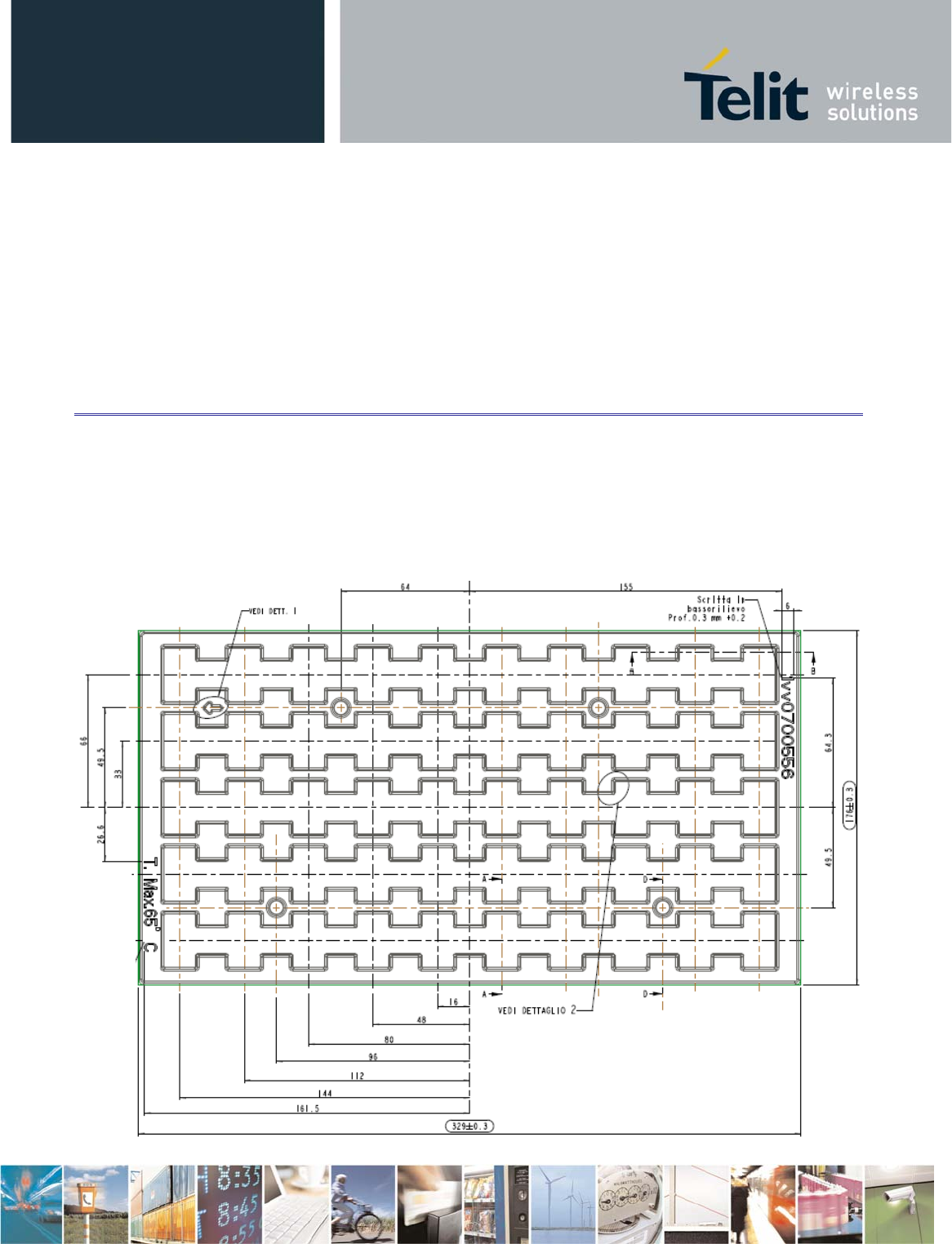
ZE51/61-2.4/SMD modules are delivered in plastic tray packaging, each tray including 50 units. The dimensions of
the tray are the following: 329 mm x 176 mm x 5.6 mm. Each unit is placed in a 26.6 mm x 16 mm location. An
empty tray weights 45 g and a loaded tray weights around 130 g.
ZE51/61-2.4 RF Module User Guide
1VV0300868 Rev.4 – 23/06/2011
Reproduction forbidden without Telit Communications S.p.A. written authorization - All Rights Reserved page 29 of 54
V.2. Storage
The optimal storage environment for ZE51/61-2.4/SMD modules should be dust free, dry and the temperature
should be included between -40°C and +85°C.
In case of a reflow soldering process, tiny radio modules must be submitted to a drying bake at +60°C during 24
hours. The drying bake must be used prior to the reflow soldering process in order to prevent a popcorn effect.
After being submitted to the drying bake, tiny modules must be soldered on host boards within 168 hours.
Also, it must be noted that due to some components, ZE51/61-2.4/SMD modules are ESD sensitive device.
Therefore, ESD handling precautions should be carefully observed.
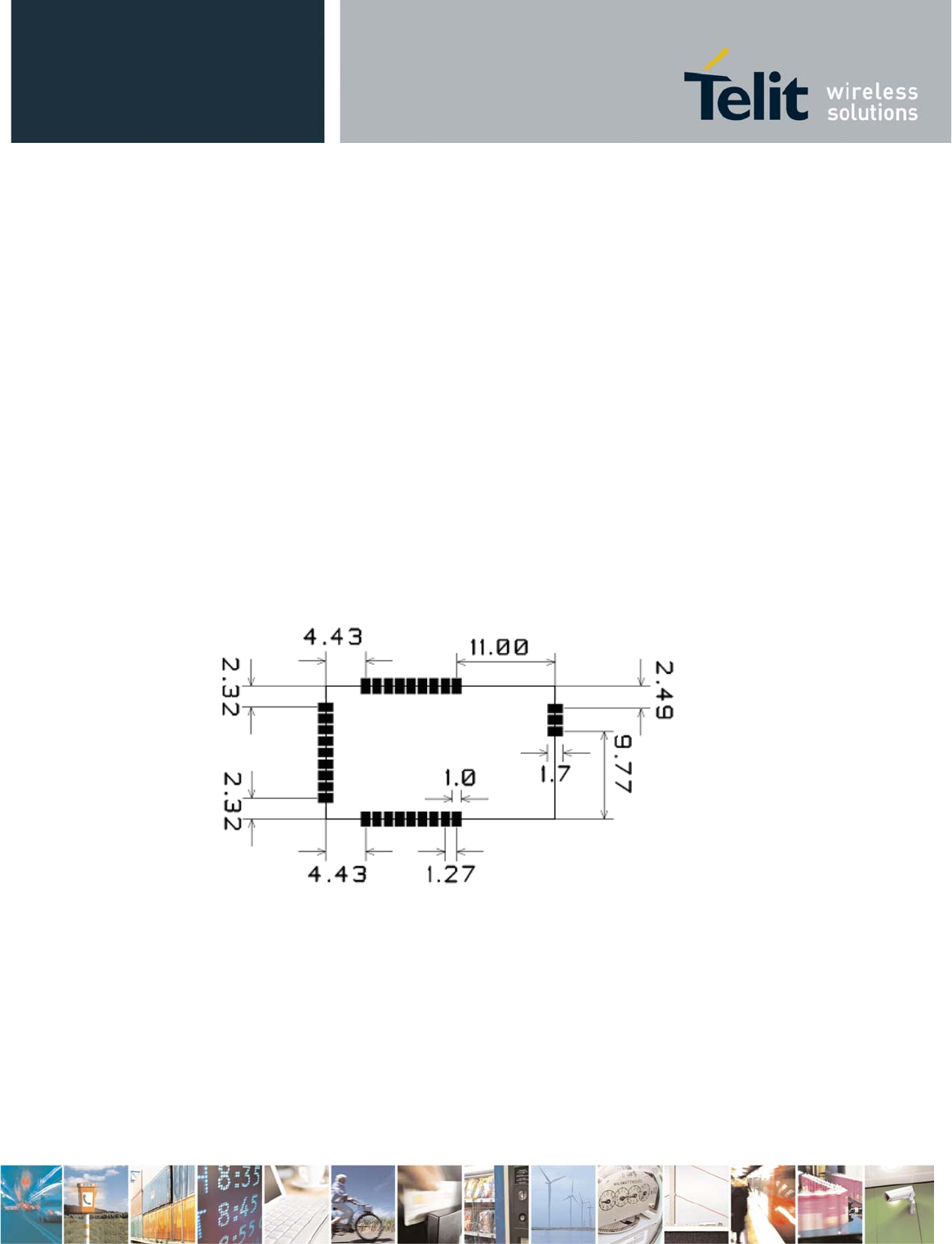
V.3. Soldering pad pattern
The surface finished on the printed circuit board pads should be made of Nickel/Gold surface.
The recommended soldering pad layout on the host board for the ZE51/61-2.4/SMD-WA, is shown in the diagram
below:
All dimensions in mm
ZE51/61-2.4 RF module User Guide
1VV0300868 Rev.4 – 23/06/2011
Reproduction forbidden without Telit Communications S.p.A. written authorization - All Rights Reserved page 30 of 54
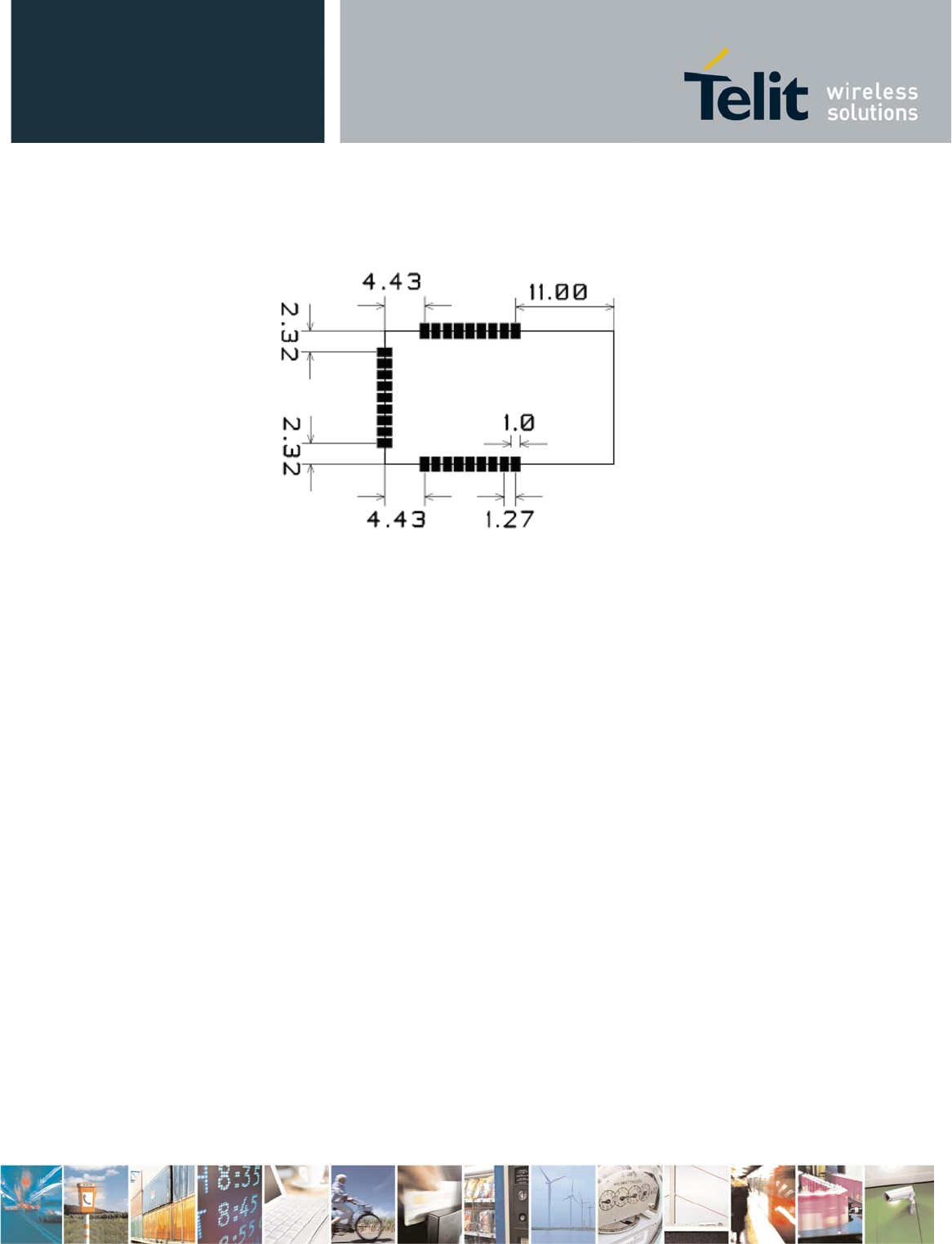
The recommended soldering pad layout on the host board for the ZE51/61-2.4/SMD-IA, is shown in the diagram
below:
All dimensions in mm
Neither via-holes nor wires are allowed on the PCB upper layer in area occupied by the module.
ZE51/61-2.4 RF Module User Guide
1VV0300868 Rev.4 – 23/06/2011
Reproduction forbidden without Telit Communications S.p.A. written authorization - All Rights Reserved page 31 of 54
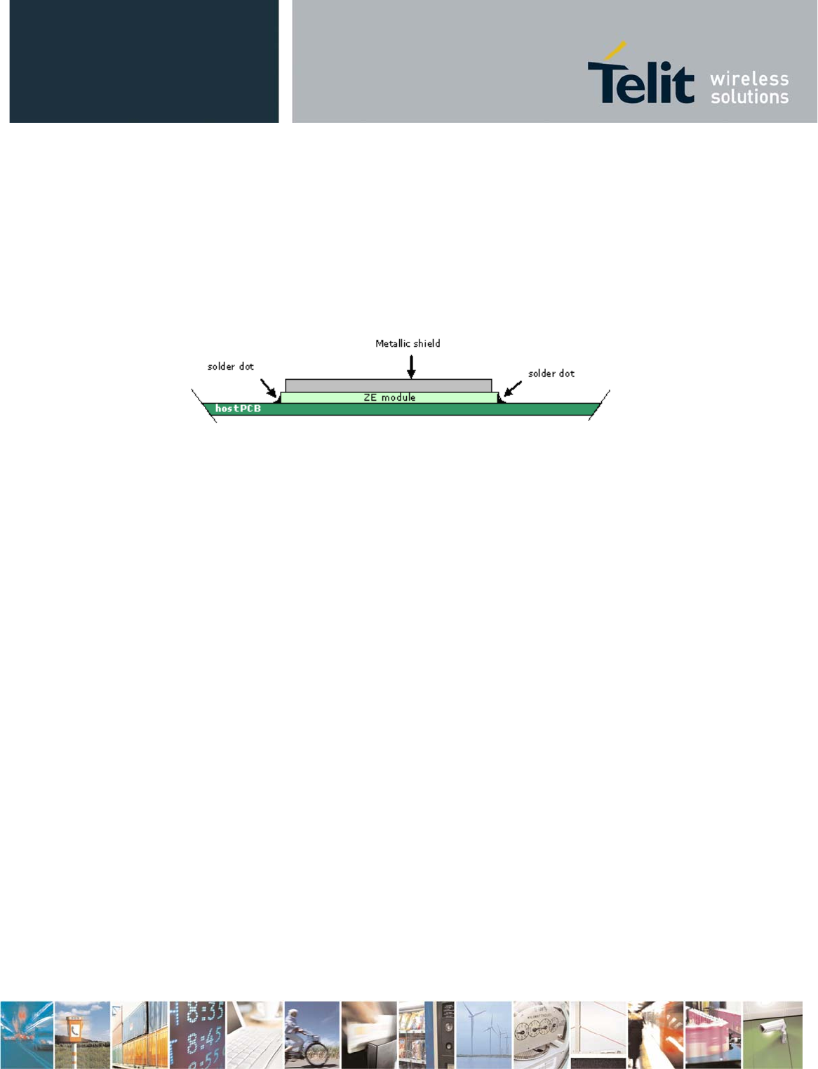
V.4. Solder paste composition (RoHS process)
ZE51/61-2.4/SMD module is designed for surface mounting using half-moon solder joints (see diagram below). For
proper module assembly, solder paste must be printed on the target surface of the host board. The solder paste
should be eutectic and made of 95.5% of SN, 4% of Ag and 0.5% of Cu. The recommended solder paste height is
180 μm .
The following diagram shows mounting characteristics for tiny integration on host PCB:
V.5. Placement
The ZE51/61-2.4/SMD module can be automatically placed on host boards by pick-and-place machines like any
integrated circuit.
ZE51/61-2.4 RF module User Guide
1VV0300868 Rev.4 – 23/06/2011
Reproduction forbidden without Telit Communications S.p.A. written authorization - All Rights Reserved page 32 of 54
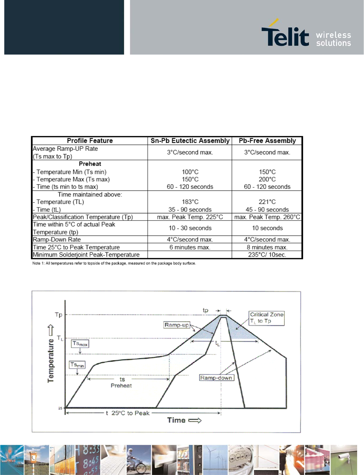
V.6. Soldering profile (RoHS process)
It must be noted that ZE51/61-2.4/SMD module should not be allowed to be hanging upside down during the reflow
operation. This means that the module has to be assembled on the side of the printed circuit board that is soldered
last.
The recommendation for lead-free solder reflow in IPC/JEDEC J-STD-020D Standard should be followed.
ZE51/61-2.4 RF Module User Guide
1VV0300868 Rev.4 – 23/06/2011
Reproduction forbidden without Telit Communications S.p.A. written authorization - All Rights Reserved page 33 of 54
The barcode label located on the module shield is able to withstand the reflow temperature.
CAUTION
It must also be noted that if the host board is submitted to a wave
soldering after the reflow operation, a solder mask must be used in
order to protect the tiny radio module’s metal shield from being in
contact with the solder wave.

ZE51/61-2.4 RF module User Guide
1VV0300868 Rev.4 – 23/06/2011
Reproduction forbidden without Telit Communications S.p.A. written authorization - All Rights Reserved page 34 of 54
CHAPTER VI. BOARD MOUNTING RECOMMENDATION
VI.1. Electrical environment
The best performances of the ZE51/61-2.4 module are obtained in a “clean noise” environment. Some basic
recommendations must be followed:
Noisy electronic components (serial RS232, DC-DC Converter, Display, Ram, bus ,...) must be placed as
far as possible from the ZE51/61-2.4 module.
Switching components circuits (especially RS-232/TTL interface circuit power supply) must be decoupled
with a 100 µF tantalum capacitor. And the decoupling capacitor must be as close as possible to the noisy
chip.
ZE51/61-2.4 RF Module User Guide
1VV0300868 Rev.4 – 23/06/2011
Reproduction forbidden without Telit Communications S.p.A. written authorization - All Rights Reserved page 35 of 54
VI.2. Power supply decoupling on ZE51/61-2.4 module
The power supply of ZE51/61-2.4 module must be nearby decoupled. A LC filter must be placed as close as
possible to the radio module power supply pin, VDD .
Symbols Reference Value Manufacturer
L1 LQH31MN1R0K03 1µH Murata
C1 GRM31CF51A226ZE01 22µF Murata
C2 Ceramic SMD 25V 100nF Multiple
Vdd
C1 C2
Power Supply
L1
ZE51/61-2.4 RF module User Guide
1VV0300868 Rev.4 – 23/06/2011
Reproduction forbidden without Telit Communications S.p.A. written authorization - All Rights Reserved page 36 of 54
VI.3. RF layout considerations
Basic recommendations must be followed to achieve a good RF layout :
It is recommended to fill all unused PCB area around the module with ground plane, except in case of
integrated antenna (no ground plane must be placed in front of the antenna and on the bottom side).
The radio module ground pin must be connected to solid ground plane.
If the ground plane is on the bottom side, a via (Metal hole) must be used in front of each ground pad.
Especially J28 and J30 (RF Gnd) pins should be grounded via several holes to be located right next to
the pins thus minimizing inductance and preventing mismatch and losses.
Example of GND layout Top View (with and without integrated antenna)
ZE51/61-2.4 RF Module User Guide
1VV0300868 Rev.4 – 23/06/2011
Reproduction forbidden without Telit Communications S.p.A. written authorization - All Rights Reserved page 37 of 54
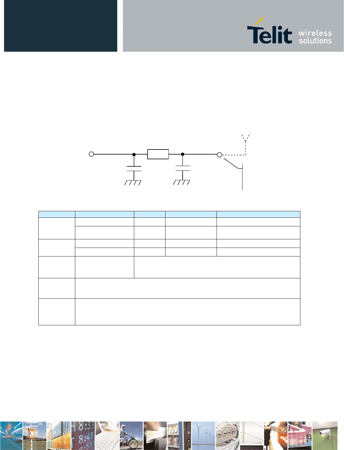
VI.4. Antenna connection on Printed Circuit Boards
Special care must be taken when connecting an antenna or a connector to the module. The RF output impedance
is 50 ohms, so the strip between the pad and the antenna or connector must be 50 ohms following the tables
below. Ground lines should be connected to the ground plane with as many vias as possible, but not too close to
the signal line.
PCB material PCB thickness H (mm) Coplanar line W (mm) Coplanar line G (mm)
FR4 0.8 1 0.3
1.6 1 0.2
Table 1 : Values for double face PCB with ground plane around and under coplanar wave guide (recommended)
PCB material PCB thickness H (mm) Coplanar line W (mm) Coplanar line G (mm)
FR4 0.8 1 0.22
1.6 1 0.23
Table 2 : Values for simple face PCB with ground plane around coplanar wave guide
(not recommended)
ZE51/61-2.4 RF module User Guide
1VV0300868 Rev.4 – 23/06/2011
Reproduction forbidden without Telit Communications S.p.A. written authorization - All Rights Reserved page 38 of 54
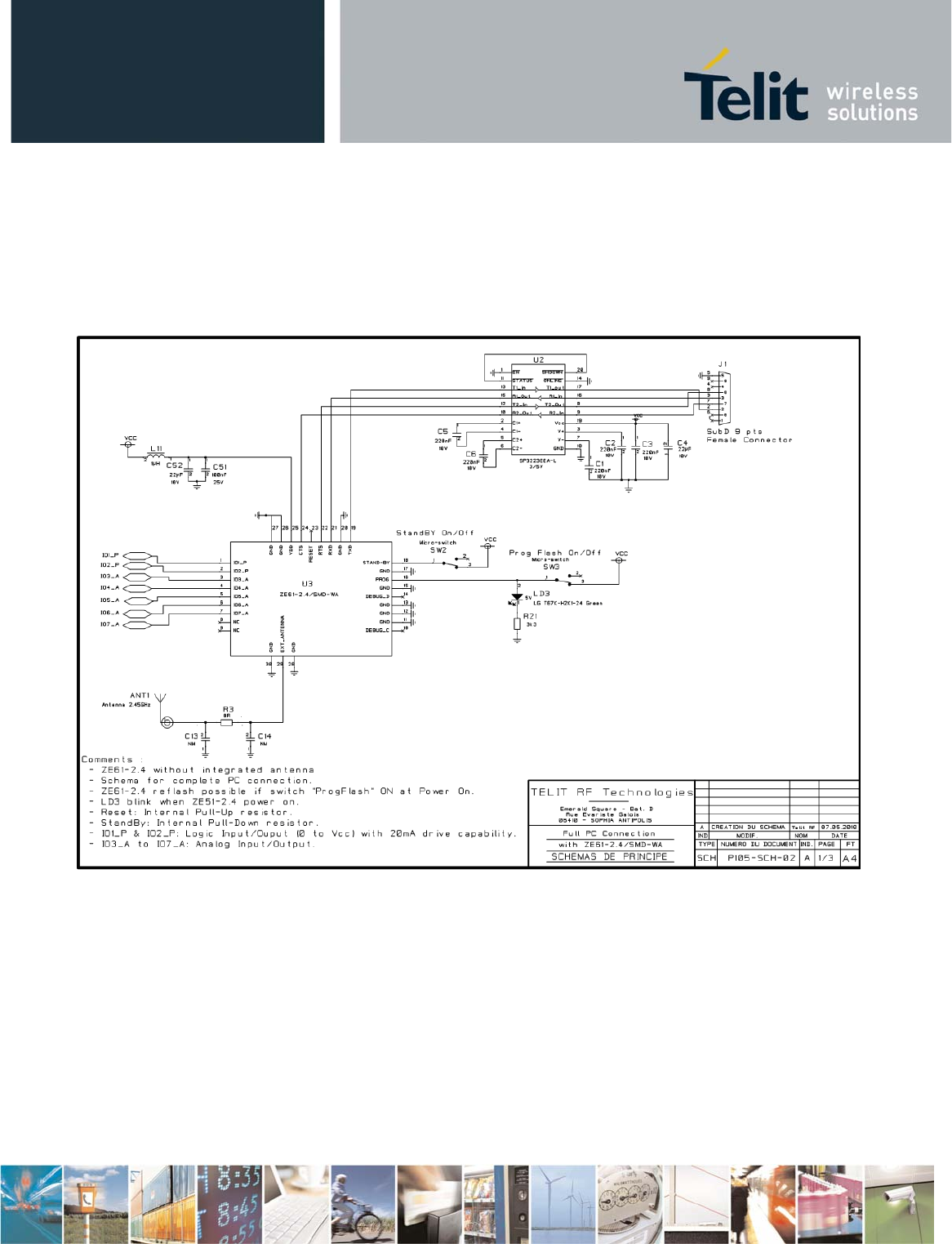
VI.5. ZE51/61-2.4 interfacing :
Example of a full RS-232 connection between a PC or an Automat (PLC) and ZE51/61-2.4/SMD-WA
ZE51/61-2.4 RF Module User Guide
1VV0300868 Rev.4 – 23/06/2011
Reproduction forbidden without Telit Communications S.p.A. written authorization - All Rights Reserved page 39 of 54
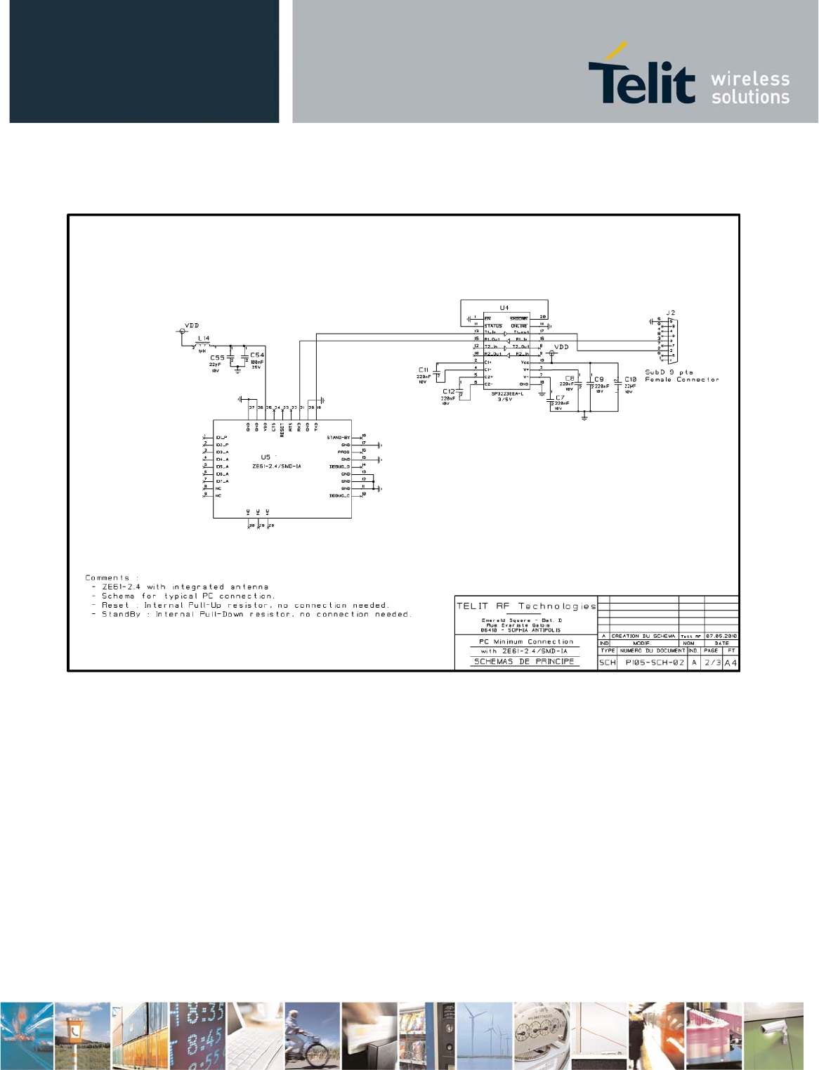
Example of a minimum PC connection with ZE51/61-2.4/SMD-IA .
ZE51/61-2.4 RF module User Guide
1VV0300868 Rev.4 – 23/06/2011
Reproduction forbidden without Telit Communications S.p.A. written authorization - All Rights Reserved page 40 of 54
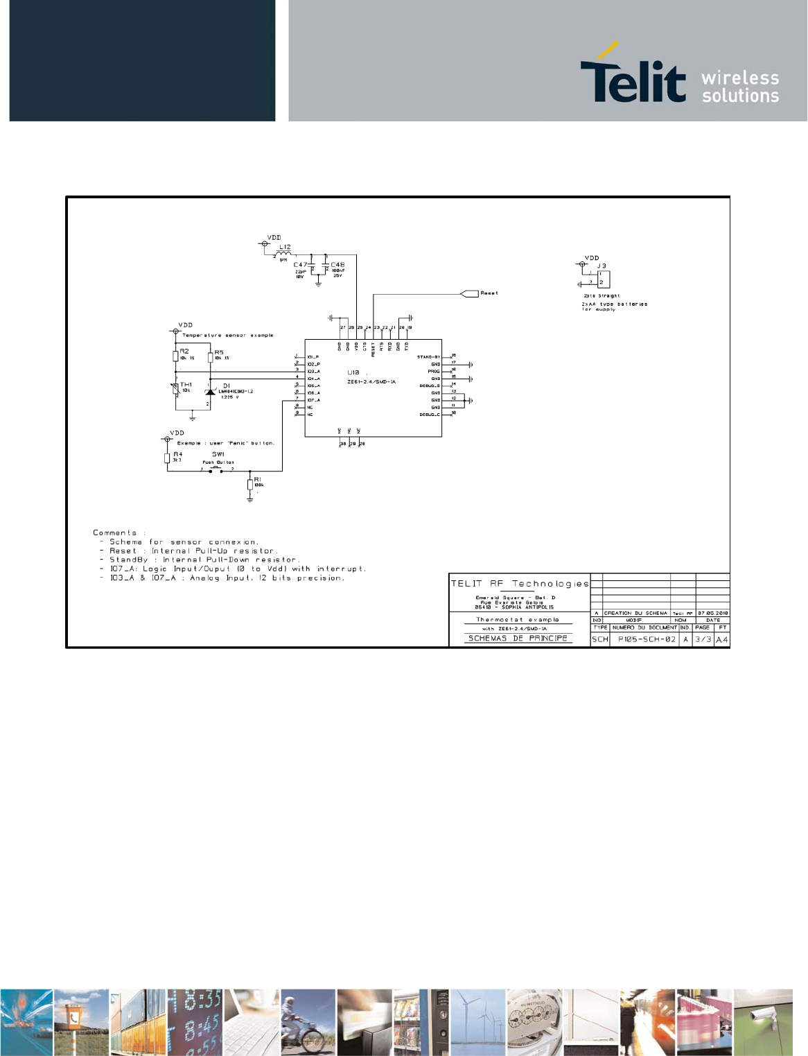
Example for sensor connection with ZE51/61-2.4/SMD-IA.

ZE51/61-2.4 RF Module User Guide
1VV0300868 Rev.4 – 23/06/2011
Reproduction forbidden without Telit Communications S.p.A. written authorization - All Rights Reserved page 41 of 54
CHAPTER VII. ANTENNA CONSIDERATIONS
VII.1. Antenna recommendations
ZE51/61-2.4 performances when used in a product are strongly dependent on the antenna type and its location.
Particular cautions are required on the following points:
Use a good and efficient antenna designed for the 2.4 GHz band.
Antenna must be fixed in such a location that electronic noise cannot affect the performances. (Outside
location is ideal if available).
Antenna directivity must be low (Omni directional antenna is usually the best choice).
Recommended antenna specifications:
Frequency Band : 2440MHz +/- 100MHz
Radiation Pattern : Omni directional
Nominal Impedance: 50
VSWR: 1.5:1 max.
Gain: 0dBi
Polarization: Vertical
ZE51/61-2.4 RF module User Guide
1VV0300868 Rev.4 – 23/06/2011
Reproduction forbidden without Telit Communications S.p.A. written authorization - All Rights Reserved page 42 of 54
VII.2. Antenna matching
Impedance matching can be required to deliver the maximum possible power from the module to the antenna and
vice versa. This is typically accomplished by inserting a matching network into a circuit between the source and the
load.
This matching network must be established as close as possible to the ZE51/61 module.
Hereafter an example of matching network used on the DIP interface board :
Symbols Reference Package Value Comments
Z1 *
Resistor 0603 0 ohm ZE51-2.4/DIP-WA
Monolithic Ceramic
capacitor COG 0603 1.5 pF ZE61-2.4/DIP-WA
Z2, Z3 * - - Not mounted ZE51-2.4/DIP-WA
- - Not mounted ZE61-2.4/DIP-WA
Track 1,
Track 2 Coplanar Waveguide
Track 1 length (as short as possible)
Track 2 length (as short as possible)
Plated holes
Ground vias :
drill of 0,35 mm
pad of 0,75 mm
Antenna
connection
Coaxial cable Pad:
Hot point: 2*2mm
Ground pad:2*4mm
Or a specific SMA connector can be used.
*: These values should be measured and optimized with a Network Analyzer. If no impedance matching is
necessary, replace Z1 by a 0 ohm resistor, and let Z2 and Z3 not mounted.
See the layouts §VI.3 to have an idea of the antenna matching implantation.
Antenna
Connection
Z3
Z2
J29 RF
Input/Output Z1
Track 1 Track 2
ZE51/61-2.4 RF Module User Guide
1VV0300868 Rev.4 – 23/06/2011
Reproduction forbidden without Telit Communications S.p.A. written authorization - All Rights Reserved page 43 of 54
VII.3. Antenna types
The following are the antenna examples that may be suitable for ZE51/61-2.4/SMD-WA applications. We
distinguish two types of antenna:
External antenna (antenna is mounted outside of the device)
Embeddable antenna (antenna is integrated inside the device)
VII.4. External antenna
External antenna is recommended when the range performance is primordial. For example, for base stations and
access points, where a better antenna gain may be required.
¼ Wave Monopole antenna:
The ¼ Wave antenna is 3 cm long @ 2.4 Ghz. Shorter compensated antennas could be used as long as they are
adapted to 2.4 GHz frequency.
Best range may be achieved if the ¼ Wave antenna is placed perpendicular in the middle of a solid ground plane
measuring at least 5 cm radius. In this case, the antenna should be connected to the module via some 50 ohm
characteristic impedance coaxial cable.
WARNING
The metallic plane must be ideally under the antenna (balanced radiation). Never
short-circuit the hot and cold pins!
The installation directives are the following:
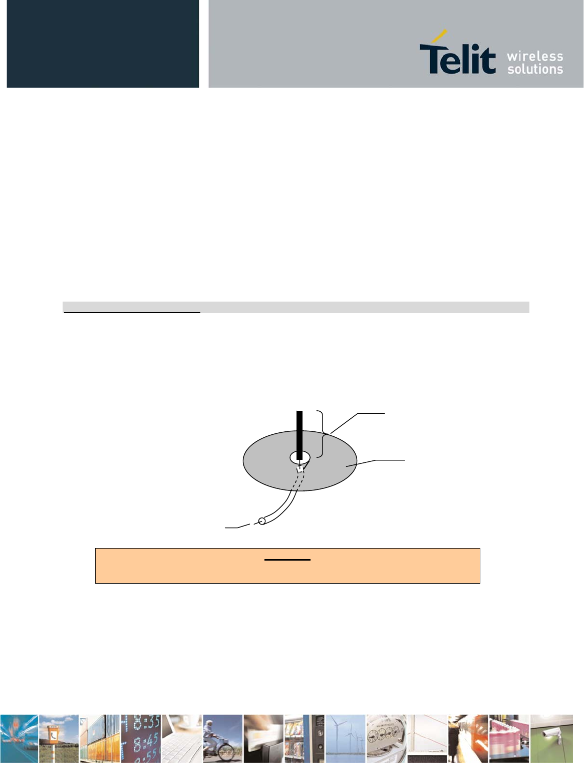
Solder the coaxial cable on the hot and ground pad antenna (of the ZE51/61-2.4 module.)
Fix the antenna on a metallic plane or on a metallic box with the metallic screw provided with the antenna.
If the ZE51/61-2.4 module is integrated in a plastic box, use a metal tape (copper) glued on the plastic
side under the antenna.
Coaxial hot and ground soldered
on the ZE51 RF output
Ground plane
connected to coaxial
ground
¼ Wave Antenna,
connected to hot point.
ZE51/61-2.4 RF module User Guide
1VV0300868 Rev.4 – 23/06/2011
Reproduction forbidden without Telit Communications S.p.A. written authorization - All Rights Reserved page 44 of 54
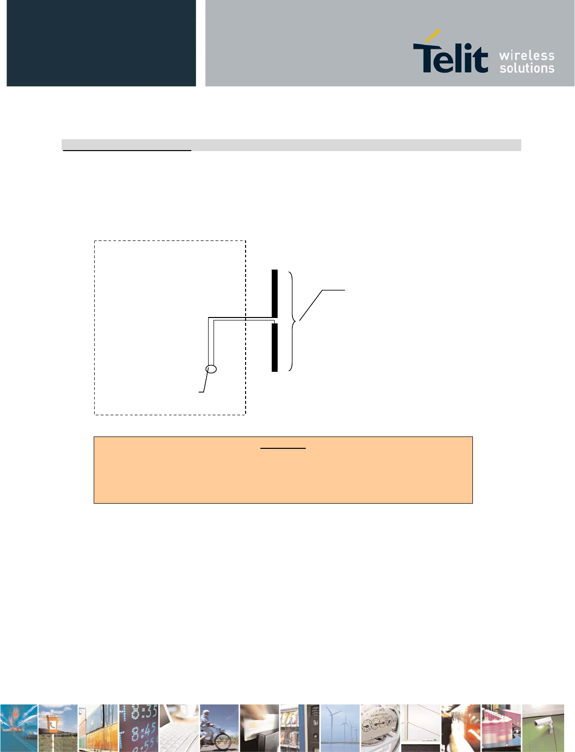
Half Wave Dipole antenna:
The ½ Wave Dipole antenna is around 6 cm long. In a ½ Wave Dipole antenna the metallic plane is replaced by a
second ¼ Wave antenna balancing the radiation.
Half wave monopole antenna typically offers a ground-independent design with favorable gain, excellent radiation
pattern. It has a high impedance and requires an impedance-matching circuit (See paragraph IX.3)
WARNING
It is recommended to place the ½ wave dipole antenna away from all metallic
object, which will detuned it.
Particularity it is not recommended to place this type of antenna directly on a
metallic box, but the antenna can be deported away through a 50 ohm coaxial
cable.
1/2 wave antenna
Core linked to hot point
Coaxial hot and ground
plug on the tiny RF
output
Box
ZE51/61-2.4 RF Module User Guide
1VV0300868 Rev.4 – 23/06/2011
Reproduction forbidden without Telit Communications S.p.A. written authorization - All Rights Reserved page 45 of 54
VII.5. Embeddable antennas
In this section you will find antennas designed to be directly attached to ZE51/61-2.4/SMD-WA module, inside the
product casing. These antennas are only used in application where security, cosmetics, size or environmental
issues make an external antenna impractical. This type of antenna is used when the integration factor becomes
primordial (for mobile and handheld devices) to the range performances.
The basic recommendations are:
The radio module must not be placed in a metallic casing or close to metallic devices.
The internal antenna must be far from noisy electronic.
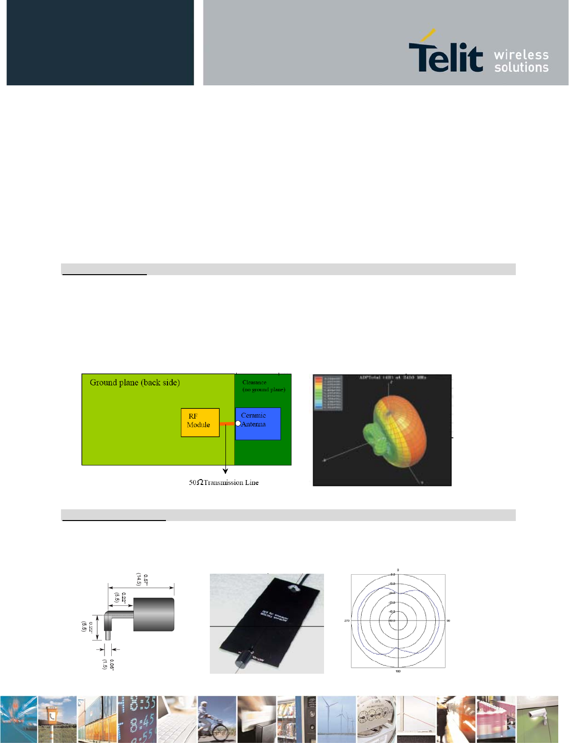
Ceramic antenna:
Ceramic antenna is a SMD component to be mounted directly on the PCB. It is designed so that it resonates and
be 50 ohms at the desired frequency. But we recommended to place an impedance-matching circuit (See
paragraph VII.2).
The place under and around the ceramic antenna must be free of any track or ground plane. (refer to the antenna
constructor requirements). It usually has a hemispherical radiation pattern has described below.
Miniaturized antenna:
This type of antenna features a through-hole feedline to directly attach it to the PCB. This antenna acts like a ¼
wave antenna so that a minimum ground plane is required.
ZE51/61-2.4 RF module User Guide
1VV0300868 Rev.4 – 23/06/2011
Reproduction forbidden without Telit Communications S.p.A. written authorization - All Rights Reserved page 46 of 54
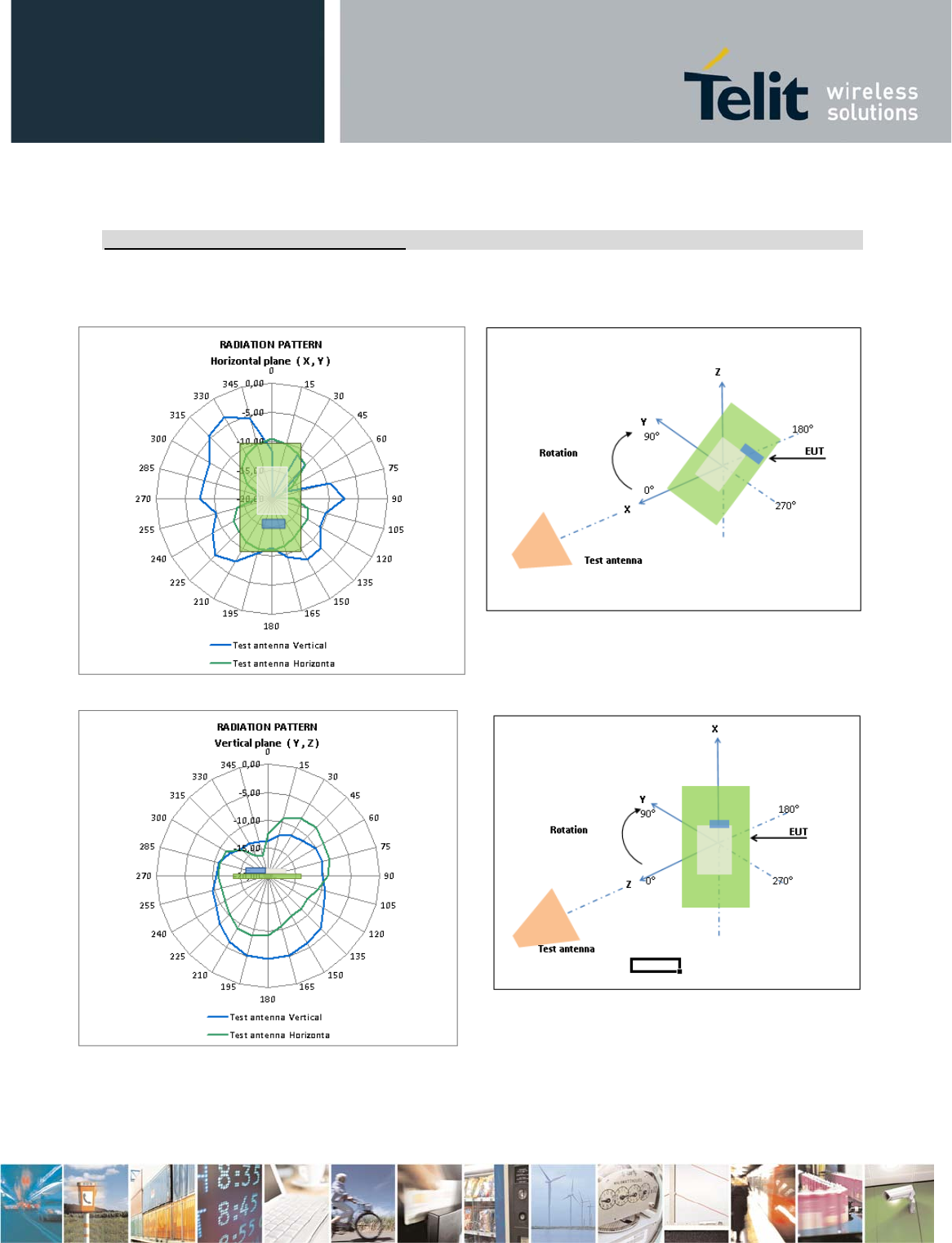
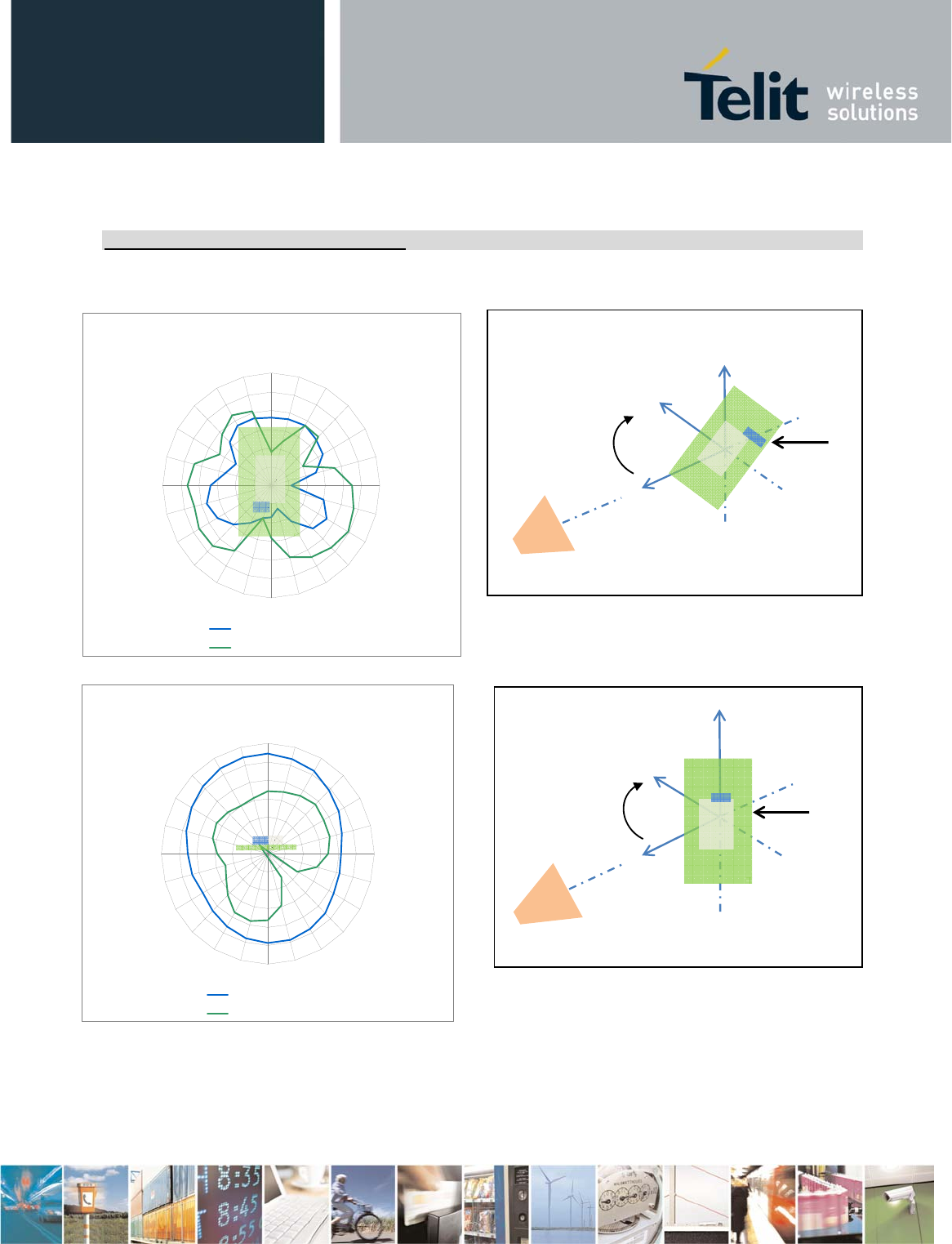
ZE51-2.4/SMD-IA: Integrated antenna:
ZE51-2.4 module is available with an integrated chip antenna, allowing very compact integration for small space
application.
Radiation Pattern of ZE51-2.4/DIP board
It is very important to avoid ground plane around and below the antenna, so ZE51-2.4/SMD-IA must be
implemented as described in paragraph VI.3 and schematics VI.5.
ZE51/61-2.4 RF Module User Guide
1VV0300868 Rev.4 – 23/06/2011
Reproduction forbidden without Telit Communications S.p.A. written authorization - All Rights Reserved page 47 of 54
ZE61-2.4/SMD-IA: Integrated antenna:
ZE61-2.4 module is available with an integrated chip antenna, allowing very compact integration for small space
application.
Radiation Pattern of ZE61-2.4/DIP board
It is very important to avoid ground plane around and below the antenna, so ZE61-2.4/SMD-IA must be
implemented as described in paragraph VI.3 and schematics VI.5.
X
Y
Z
Test
EU
Rotation
RADIATIONPATTERN
Horizontalplane(X,Y)
‐10,00
‐5,00
0,00
5,00
10,00
15,00
20,00
0
15
30
45
60
75
90
105
120
135
150
165
180
195
210
225
240
255
270
285
300
315
330
345
TestantennaVerti cal
TestantennaHorizontal
EUT
X
Y
Z
Test antenna
Rotation
RADIATIONPATTERN
Verticalplane(Y,Z)
‐10,00
‐5,00
0,00
5,00
10,00
15,00
20,00
0
15
30
45
60
75
90
105
120
135
150
165
180
195
210
225
240
255
270
285
300
315
330
345
TestantennaVertical
TestantennaHorizontal
ZE51/61-2.4 RF module User Guide
1VV0300868 Rev.4 – 23/06/2011
Reproduction forbidden without Telit Communications S.p.A. written authorization - All Rights Reserved page 48 of 54
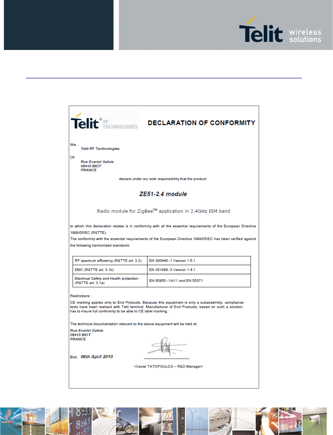
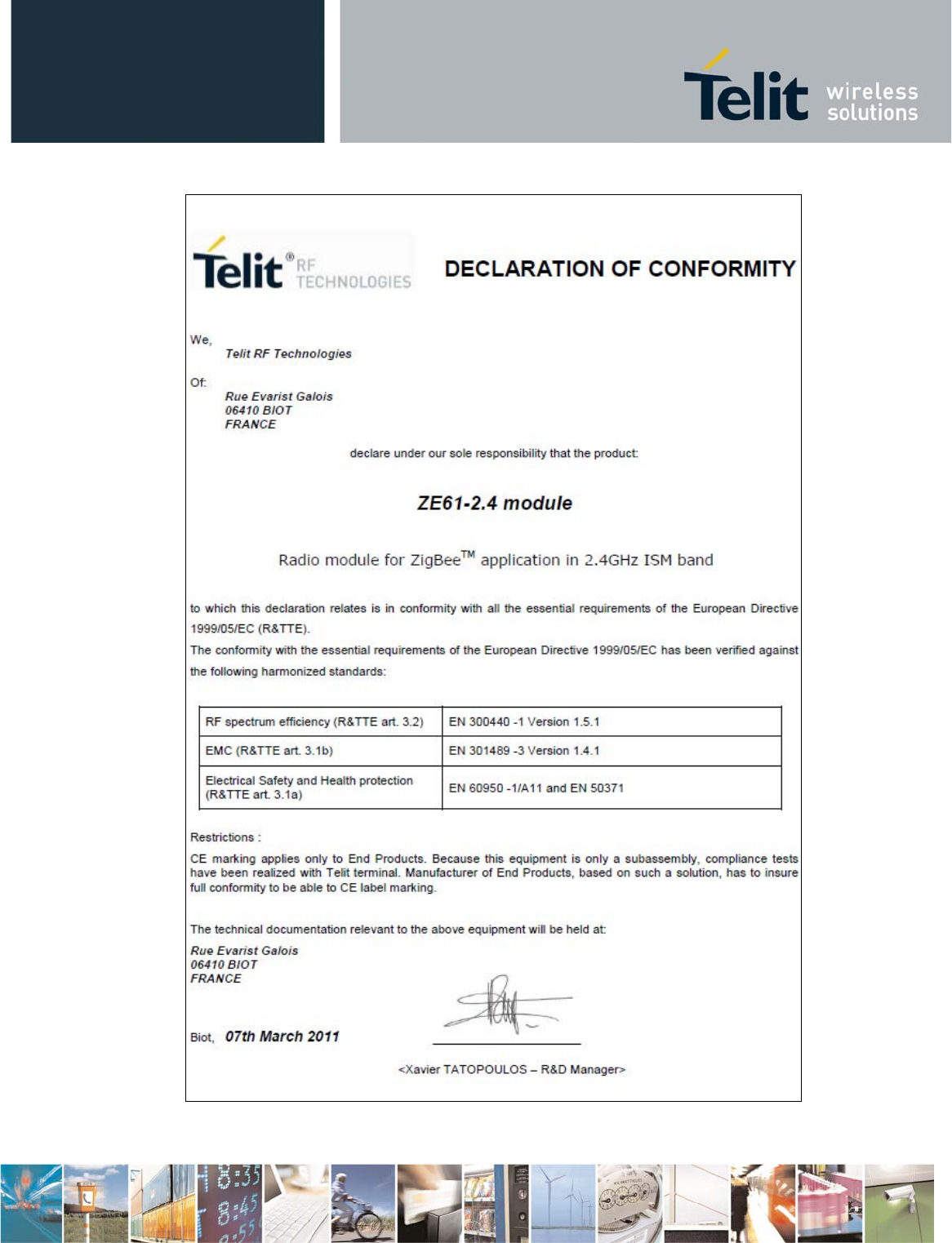
CHAPTER VIII. ANNEXES
VIII.1. Declaration of Conformity
ZE51/61-2.4 RF Module User Guide
1VV0300868 Rev.4 – 23/06/2011
Reproduction forbidden without Telit Communications S.p.A. written authorization - All Rights Reserved page 49 of 54
ZE51/61-2.4 RF module User Guide
1VV0300868 Rev.4 – 23/06/2011
Reproduction forbidden without Telit Communications S.p.A. written authorization - All Rights Reserved page 50 of 54
ZE51/61-2.4 RF Module User Guide
1VV0300868 Rev.4 – 23/06/2011
Reproduction forbidden without Telit Communications S.p.A. written authorization - All Rights Reserved page 51 of 54

ZE51/61-2.4 RF module User Guide
1VV0300868 Rev.4 – 23/06/2011
Reproduction forbidden without Telit Communications S.p.A. written authorization - All Rights Reserved page 52 of 54
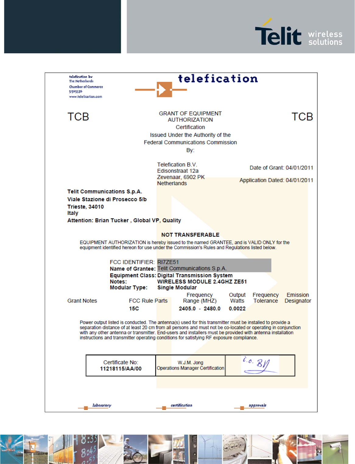
VIII.2. Conformity Assessment Issues FCC/IC
Modules ZE51/61 are FCC/IC approved as modules to be installed in other devices. If the final product after
integration is intended for portable use, a new application and FCC/IC is required.
FCC Notice
The FCC notifies users that any changes or modifications made to this device that are not expressly approved by
Telit Communications S.P.A. may void the user’s authority to operate the equipment.
This equipment has been tested and found to comply with the limits for a Class B digital device, pursuant to part 15
of the FCC Rules. These limits are designed to provide reasonable protection against harmful interference in a
residential installation. This equipment generates, uses and can radiate radio frequency energy and, if not installed
and used in accordance with the instructions, may cause harmful interference to radio communications. However,
there is no guarantee that interference will not occur in a particular installation. If this equipment does cause
harmful interference to radio or television reception, which can be determined by turning the equipment off and on,
the user is encouraged to try to correct the interference by one or more of the following measures:
- Reorient or relocate the receiving antenna.
- Increase the separation between the equipment and receiver.
- Connect the equipment into an outlet on a circuit different from that to which the receiver is connected.
- Consult the dealer or an experienced radio/TV technician for help.
Wireless notice:
This product emits radio frequency energy, but the radiated output power of this device is far below the FCC radio
frequency exposure limits. This equipment complies with FCC RF radiation exposure limits forth for an uncontrolled
environment. Nevertheless, the device should be used in such a manner that the potential for human contact with
the antenna during normal operation is minimized.
IC Notice
This Class B digital apparatus complies with Canadian ICES-003, RSS-Gen and RSS-210.
Cet appareil numérique de la classe B est conforme à la norme NMB-003, CNR-Gen et CNR-210 du
Canada
These radio transmitters ID: 5131A-ZE51 and 5131A-XE61 has been approved by Industry Canada to operate with
the antenna types listed below with the maximum permissible gain and required antenna impedance for each
antenna type indicated. Antenna types not included in this list, having a gain greater than the maximum gain
indicated for that type, are strictly prohibited for use with this device.
Les présent émetteures radio ID: 5131A-ZE51 e 5131A-XE61 a été approuvé par Industrie Canada pour
fonctionner avec les types d'antenne énumérés ci-dessous et ayant un gain admissible maximal et l'impédance
requise pour chaque type d'antenne. Les types d'antenne non inclus dans cette liste, ou dont le gain est supérieur
au gain maximal indiqué, sont strictement interdits pour l'exploitation de l'émetteur.
Fractus Micro Reach Xtend
TM
Chip antenna
Taoglas Dipole Stub
Antenna gain 2 dBi 5 dBi
Antenna impedance 50 50
ZE51/61-2.4 RF Module User Guide
1VV0300868 Rev.4 – 23/06/2011
Reproduction forbidden without Telit Communications S.p.A. written authorization - All Rights Reserved page 53 of 54
Wireless notice
This device complies with Industry Canada licence-exempt RSS standard(s). Operation is subject to the following
two conditions: (1) this device may not cause interference, and (2) this device must accept any interference,
including interference that may cause undesired operation of the device.
Le présent appareil est conforme aux CNR d'Industrie Canada applicables aux appareils radio exempts de licence.
L'exploitation est autorisée aux deux conditions suivantes : (1) l'appareil ne doit pas produire de brouillage, et (2)
l'utilisateur de l'appareil doit accepter tout brouillage radioélectrique subi, même si le brouillage est susceptible d'en
compromettre le fonctionnement.
Label recommendations
If neither FCC ID nor IC ID is visible when the module is installed inside another device, then the outside of the
device into which the module is installed will display a label referring to the enclosed module by labelling the host
device in this manner: “Contains FCC ID: RI7ZE51 and IC ID: 5131A -ZE51” or “Contains FCC ID: RI7XE61 and
IC ID: 5131A –XE61”
Safety recommendations
The device must maintain a distance of at least 20 cm from the user’s body when transmitting. In case this
requirement cannot be satisfied, the system integrator has to assess the final product against the SAR
regulation.
VIII.3. Examples of propagation attenuation
Factor 433 MHz 868 MHz 2.4 GHz
Attenuation Attenuation Attenuation
Open office 0 dB 0 dB 0 dB
Window < 1 dB 1 – 2 dB 3 dB
Thin wall (plaster) 3 dB 3 – 4 dB 5 – 8 dB
Medium wall (wood) 4 – 6 dB 5 – 8 dB 10 – 12 dB
Thick wall (concrete) 5 – 8 dB 9 – 11 dB 15 – 20 dB
Armoured wall (reinforced concrete) 10 – 12 dB 12 – 15 dB 20 – 25 dB
Floor or ceiling 5 – 8 dB 9 – 11 dB 15 – 20 dB
Armoured floor or ceiling 10 – 12 dB 12 – 15 dB 20 – 25 dB
Rain and/or Fog 20 – 25 dB 25 – 30 dB *
* = Attenuations increase along with the frequency. In some cases, it
is therefore difficult to determine loss and attenuation value.
Note = The table above is only indicative. The real values will depend on
the installation environment itself.
ZE51/61-2.4 RF module User Guide
1VV0300868 Rev.4 – 23/06/2011
Reproduction forbidden without Telit Communications S.p.A. written authorization - All Rights Reserved page 54 of 54
VIII.4. Output power programming
The results are measured on the ZE61-2.4/DIP interface with T = 25°C, Vdd = 3 V, 2440 Mhz, 50 ohm
impedance if nothing else noted.
TxPower register
ATS202 Power (dBm) Current (dBm) Comments
0 20 175 Not recommended
1 19.5 160 Default value
2 19 145
3 18.5 135
4 17.5 124
5 16.5 113
6 15 102
7 14 96
8 12.5 89
9 11 84
10 9 80