Telit Communications S p A XE866A1NA LTE Module User Manual
Telit Communications S.p.A. LTE Module
UserManual.wiki
>
Telit Communications S p A
>
XE866A1NA User Manual
User manual
Navigation menu
Upload a User Manual
Namespaces
Wiki Guide
HTML
PDF
Info
Views
User Manual
Discussion / Help
Navigation
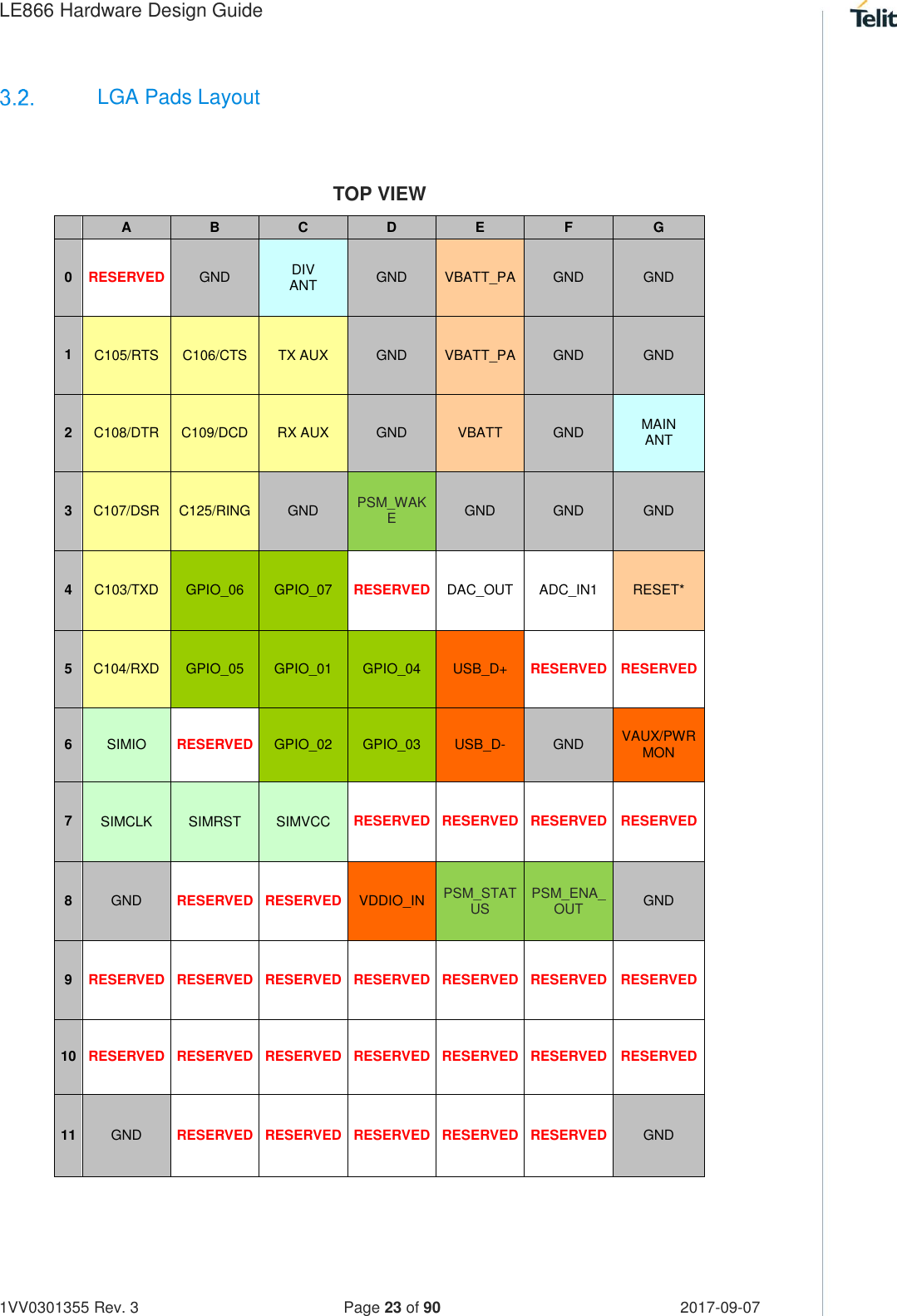
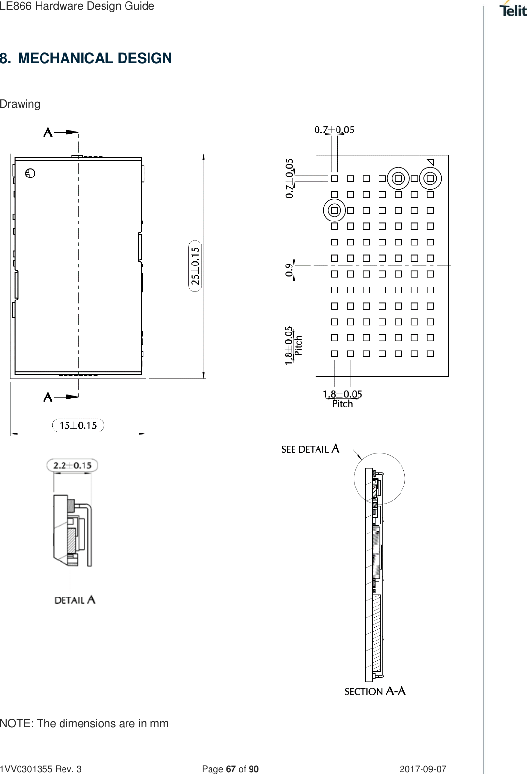
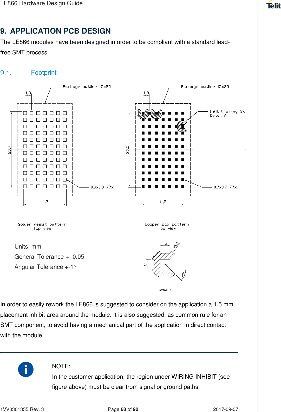
![[01.2017] Mod.0818 2017-01 Rev.0 LE866 Hardware Design Guide 1VV0301355 Rev. 3 – 2017-09-07](https://usermanual.wiki/Telit-Communications-S-p-A/XE866A1NA/User-Guide-3548968-Page-1.png)
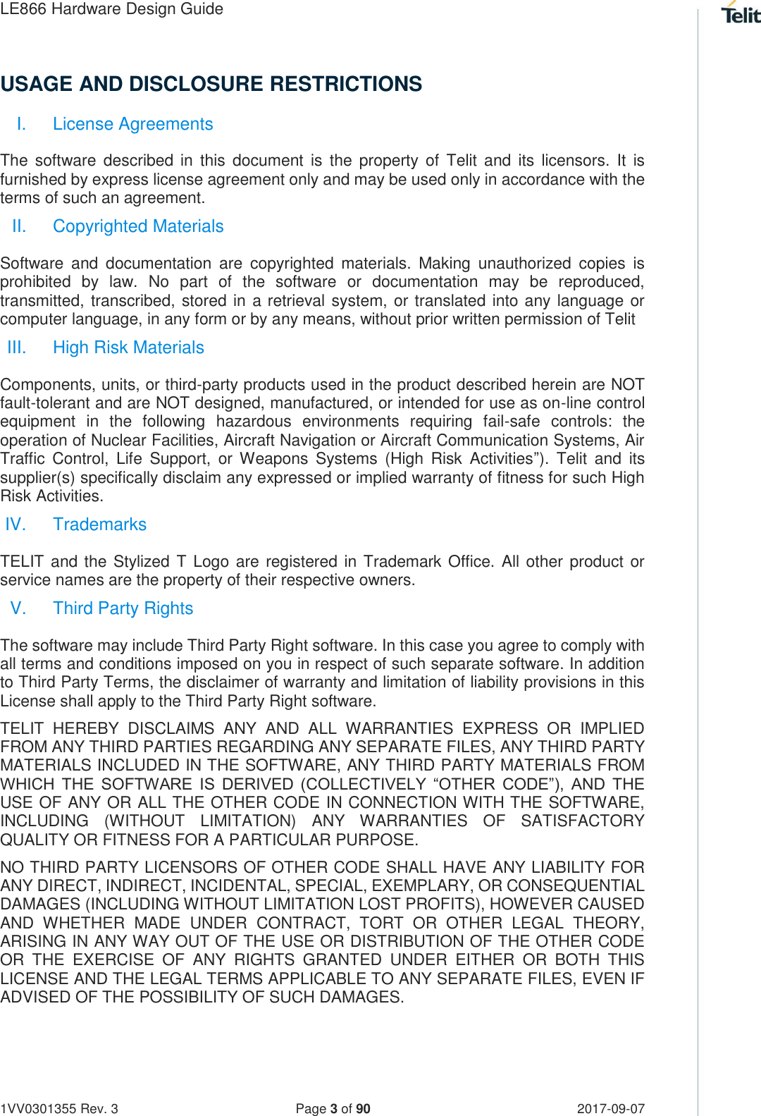
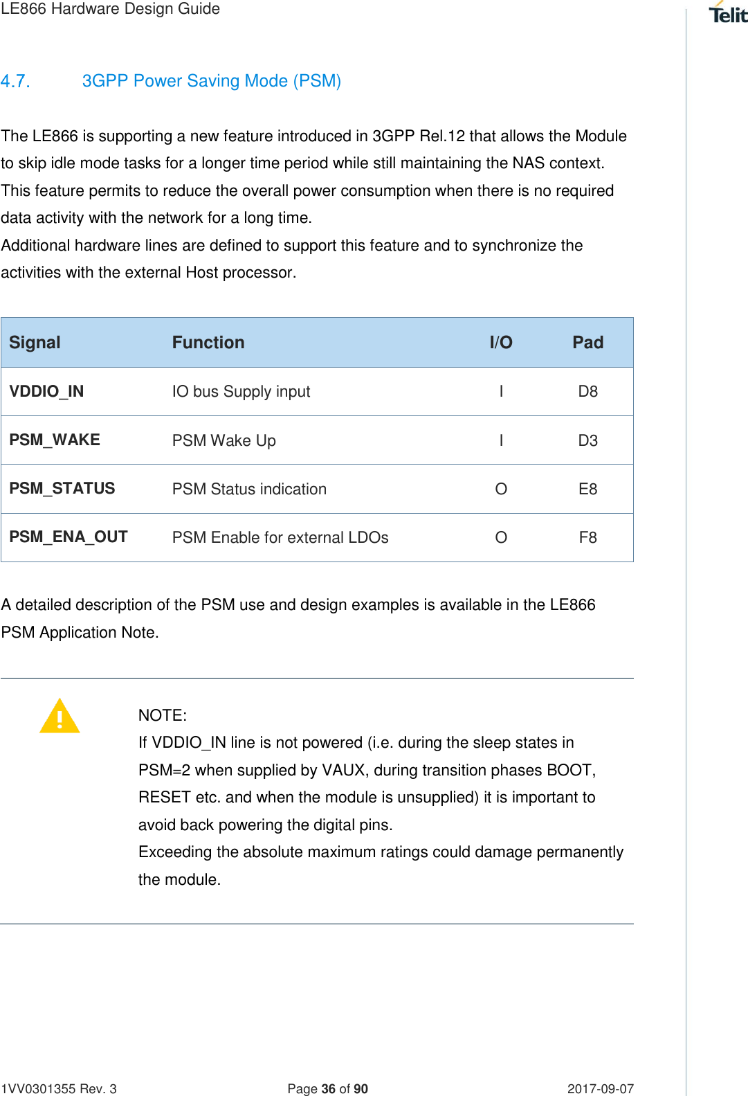
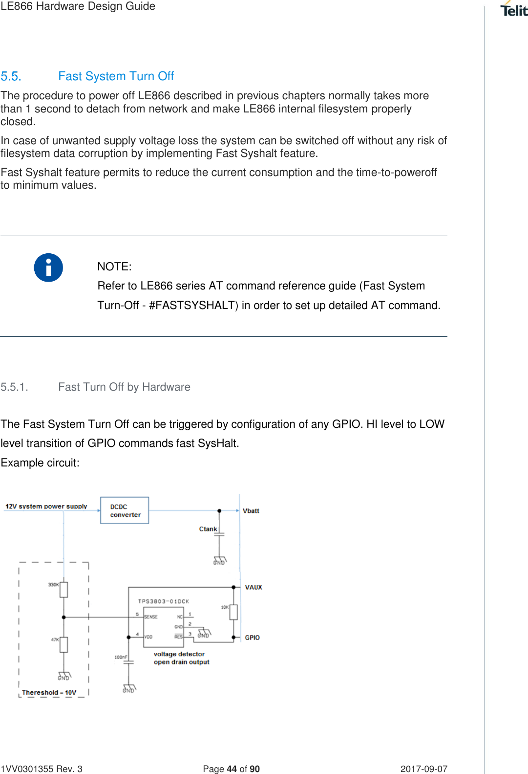
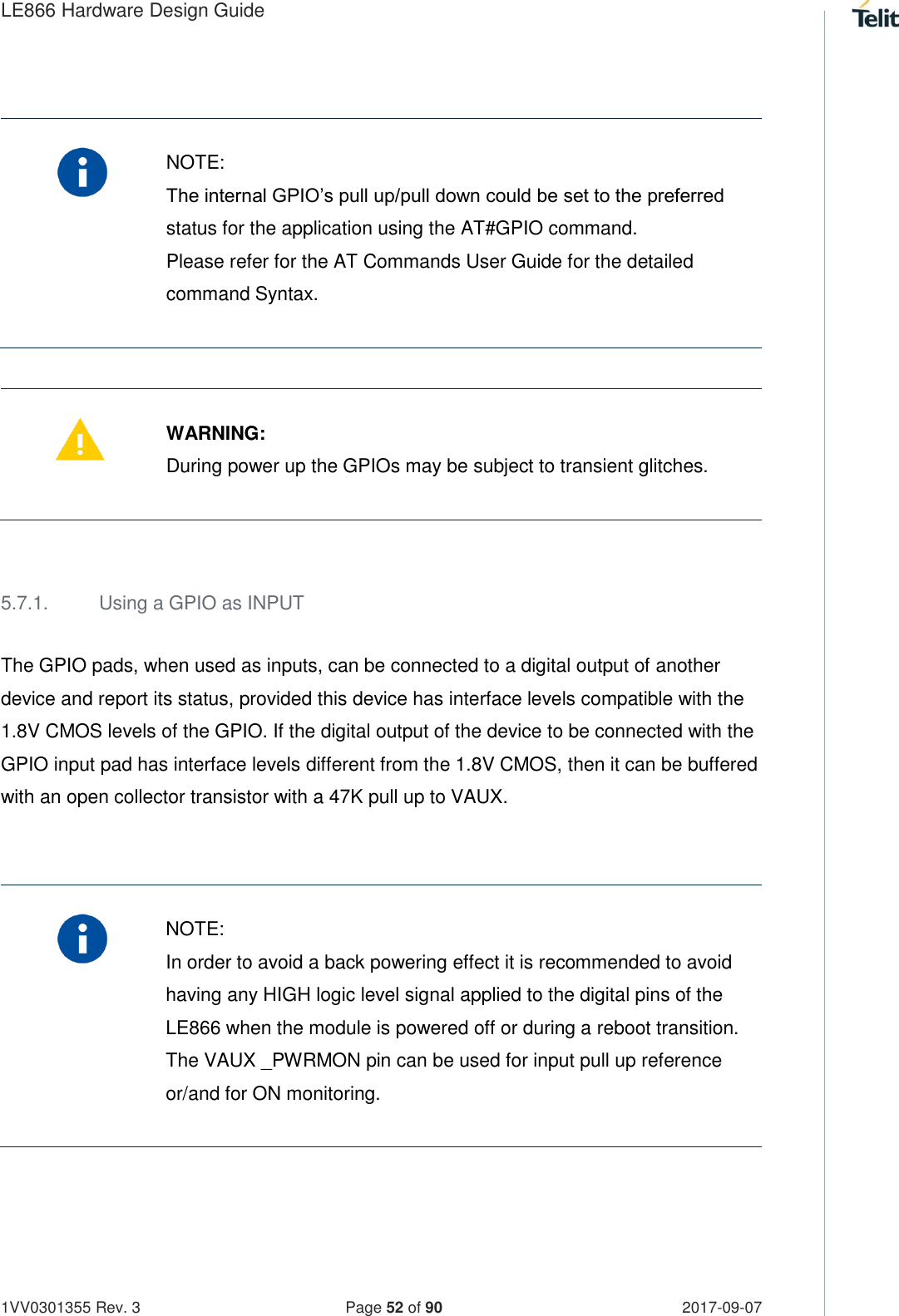
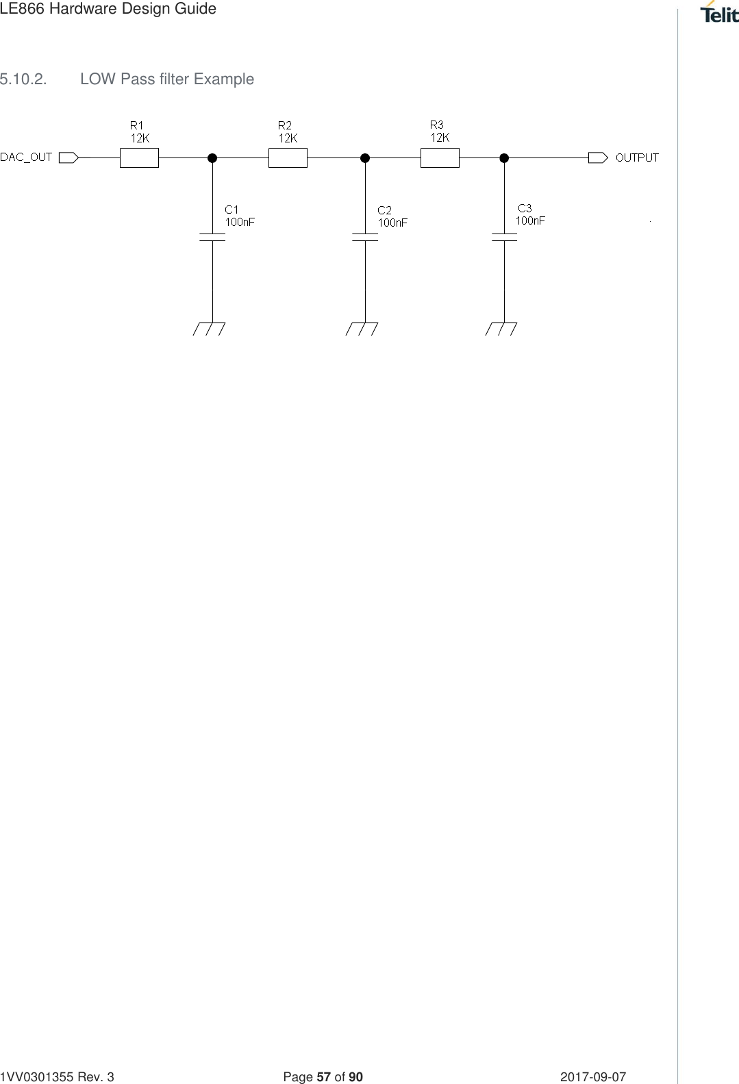
![LE866 Hardware Design Guide 1VV0301355 Rev. 3 Page 56 of 90 2017-09-07 DAC Converter The LE866 provides a Digital to Analog Converter. The signal (named DAC_OUT) is available on pin E4 of the LE866. The on board DAC is a 10 bit converter, able to generate an analogue value based on a specific input in the range from 0 up to 1023. However, an external low-pass filter is necessary. The following table is showing the ADC characteristics: Item Min Max Unit Voltage range (filtered) 0 1.8 Volt Range 0 1023 Steps The precision is 10 bits so, if we consider that the maximum voltage is 2V, the integrated voltage could be calculated with the following formula: Integrated output voltage = (2 *value) / 1023 DAC_OUT line must be integrated (for example with a low band pass filter) in order to obtain an analog voltage. 5.10.1. Enabling DAC An AT command is available to use the DAC function. The command is: AT#DAC= [<enable> [, <value>]] <value> - scale factor of the integrated output voltage (0..1023 – 10 bit precision) it must be present if <enable>=1 Refer to SW User Guide or AT Commands Reference Guide for the full description of this function. NOTE: The DAC frequency is selected internally. D/A converter must not be used during POWERSAVING.](https://usermanual.wiki/Telit-Communications-S-p-A/XE866A1NA/User-Guide-3548968-Page-56.png)
![[01.2017] Mod.0818 2017-01 Rev.0](https://usermanual.wiki/Telit-Communications-S-p-A/XE866A1NA/User-Guide-3548968-Page-90.png)