Telit Communications S p A XE866A1NA LTE Module User Manual
Telit Communications S.p.A. LTE Module
User manual

[01.2017]
Mod.0818 2017-01 Rev.0
LE866
Hardware Design Guide
1VV0301355 Rev. 3 – 2017-09-07

LE866 Hardware Design Guide
1VV0301355 Rev. 3 Page 2 of 90 2017-09-07
SPECIFICATIONS ARE SUBJECT TO CHANGE WITHOUT NOTICE
NOTICE
While reasonable efforts have been made to assure the accuracy of this document, Telit
assumes no liability resulting from any inaccuracies or omissions in this document, or from
use of the information obtained herein. The information in this document has been carefully
checked and is believed to be reliable. However, no responsibility is assumed for
inaccuracies or omissions. Telit reserves the right to make changes to any products
described herein and reserves the right to revise this document and to make changes from
time to time in content hereof with no obligation to notify any person of revisions or changes.
Telit does not assume any liability arising out of the application or use of any product,
software, or circuit described herein; neither does it convey license under its patent rights
or the rights of others.
It is possible that this publication may contain references to, or information about Telit
products (machines and programs), programming, or services that are not announced in
your country. Such references or information must not be construed to mean that Telit
intends to announce such Telit products, programming, or services in your country.
COPYRIGHTS
This instruction manual and the Telit products described in this instruction manual may be,
include or describe copyrighted Telit material, such as computer programs stored in
semiconductor memories or other media. Laws in the Italy and other countries preserve for
Telit and its licensors certain exclusive rights for copyrighted material, including the
exclusive right to copy, reproduce in any form, distribute and make derivative works of the
copyrighted material. Accordingly, any copyrighted material of Telit and its licensors
contained herein or in the Telit products described in this instruction manual may not be
copied, reproduced, distributed, merged or modified in any manner without the express
written permission of Telit. Furthermore, the purchase of Telit products shall not be deemed
to grant either directly or by implication, estoppel, or otherwise, any license under the
copyrights, patents or patent applications of Telit, as arises by operation of law in the sale
of a product.
COMPUTER SOFTWARE COPYRIGHTS
The Telit and 3rd Party supplied Software (SW) products described in this instruction manual
may include copyrighted Telit and other 3rd Party supplied computer programs stored in
semiconductor memories or other media. Laws in the Italy and other countries preserve for
Telit and other 3rd Party supplied SW certain exclusive rights for copyrighted computer
programs, including the exclusive right to copy or reproduce in any form the copyrighted
computer program. Accordingly, any copyrighted Telit or other 3rd Party supplied SW
computer programs contained in the Telit products described in this instruction manual may
not be copied (reverse engineered) or reproduced in any manner without the express written
permission of Telit or the 3rd Party SW supplier. Furthermore, the purchase of Telit products
shall not be deemed to grant either directly or by implication, estoppel, or otherwise, any
license under the copyrights, patents or patent applications of Telit or other 3rd Party
supplied SW, except for the normal non-exclusive, royalty free license to use that arises by
operation of law in the sale of a product.

LE866 Hardware Design Guide
1VV0301355 Rev. 3 Page 3 of 90 2017-09-07
USAGE AND DISCLOSURE RESTRICTIONS
I. License Agreements
The software described in this document is the property of Telit and its licensors. It is
furnished by express license agreement only and may be used only in accordance with the
terms of such an agreement.
II. Copyrighted Materials
Software and documentation are copyrighted materials. Making unauthorized copies is
prohibited by law. No part of the software or documentation may be reproduced,
transmitted, transcribed, stored in a retrieval system, or translated into any language or
computer language, in any form or by any means, without prior written permission of Telit
III. High Risk Materials
Components, units, or third-party products used in the product described herein are NOT
fault-tolerant and are NOT designed, manufactured, or intended for use as on-line control
equipment in the following hazardous environments requiring fail-safe controls: the
operation of Nuclear Facilities, Aircraft Navigation or Aircraft Communication Systems, Air
Traffic Control, Life Support, or Weapons Systems (High Risk Activities”). Telit and its
supplier(s) specifically disclaim any expressed or implied warranty of fitness for such High
Risk Activities.
IV. Trademarks
TELIT and the Stylized T Logo are registered in Trademark Office. All other product or
service names are the property of their respective owners.
V. Third Party Rights
The software may include Third Party Right software. In this case you agree to comply with
all terms and conditions imposed on you in respect of such separate software. In addition
to Third Party Terms, the disclaimer of warranty and limitation of liability provisions in this
License shall apply to the Third Party Right software.
TELIT HEREBY DISCLAIMS ANY AND ALL WARRANTIES EXPRESS OR IMPLIED
FROM ANY THIRD PARTIES REGARDING ANY SEPARATE FILES, ANY THIRD PARTY
MATERIALS INCLUDED IN THE SOFTWARE, ANY THIRD PARTY MATERIALS FROM
WHICH THE SOFTWARE IS DERIVED (COLLECTIVELY “OTHER CODE”), AND THE
USE OF ANY OR ALL THE OTHER CODE IN CONNECTION WITH THE SOFTWARE,
INCLUDING (WITHOUT LIMITATION) ANY WARRANTIES OF SATISFACTORY
QUALITY OR FITNESS FOR A PARTICULAR PURPOSE.
NO THIRD PARTY LICENSORS OF OTHER CODE SHALL HAVE ANY LIABILITY FOR
ANY DIRECT, INDIRECT, INCIDENTAL, SPECIAL, EXEMPLARY, OR CONSEQUENTIAL
DAMAGES (INCLUDING WITHOUT LIMITATION LOST PROFITS), HOWEVER CAUSED
AND WHETHER MADE UNDER CONTRACT, TORT OR OTHER LEGAL THEORY,
ARISING IN ANY WAY OUT OF THE USE OR DISTRIBUTION OF THE OTHER CODE
OR THE EXERCISE OF ANY RIGHTS GRANTED UNDER EITHER OR BOTH THIS
LICENSE AND THE LEGAL TERMS APPLICABLE TO ANY SEPARATE FILES, EVEN IF
ADVISED OF THE POSSIBILITY OF SUCH DAMAGES.

LE866 Hardware Design Guide
1VV0301355 Rev. 3 Page 4 of 90 2017-09-07
APPLICABILITY TABLE
PRODUCTS
LE866-SV1
LE866A1-NA
LE866A1-KK
LE866A1-JS
LE866A1-KS
LE866 Hardware Design Guide
1VV0301355 Rev. 3 Page 5 of 90 2017-09-07
Contents
NOTICE 2
COPYRIGHTS ................................................................................................ 2
COMPUTER SOFTWARE COPYRIGHTS ...................................................... 2
USAGE AND DISCLOSURE RESTRICTIONS ............................................... 3
I. License Agreements ..................................................................... 3
II. Copyrighted Materials ................................................................... 3
III. High Risk Materials ....................................................................... 3
IV. Trademarks .................................................................................. 3
V. Third Party Rights ......................................................................... 3
APPLICABILITY TABLE ................................................................................ 4
CONTENTS .................................................................................................... 5
1. INTRODUCTION .......................................................................... 9
Scope ........................................................................................... 9
Audience....................................................................................... 9
Contact Information, Support ........................................................ 9
Text Conventions ........................................................................ 10
Related Documents .................................................................... 11
2. GENERAL PRODUCT DESCRIPTION ...................................... 12
Overview..................................................................................... 12
Product Variants and Frequency Bands ...................................... 12
Target market ............................................................................. 13
Main features .............................................................................. 13
TX Output Power ........................................................................ 14
RX Sensitivity ............................................................................. 14
Mechanical specifications ........................................................... 15
2.7.1. Dimensions ................................................................................. 15
2.7.2. Weight ........................................................................................ 15
Temperature range ..................................................................... 15
3. PINS ALLOCATION ................................................................... 16
Pin-out ........................................................................................ 16
LGA Pads Layout ........................................................................ 23
LE866 Hardware Design Guide
1VV0301355 Rev. 3 Page 6 of 90 2017-09-07
4. POWER SUPPLY ....................................................................... 24
Power Supply Requirements ....................................................... 24
Power Consumption ................................................................... 25
General Design Rules ................................................................. 26
4.3.1. Electrical Design Guidelines ....................................................... 26
4.3.1.1. +5V Source Power Supply Design Guidelines ............................ 26
4.3.2. +12V Source Power Supply Design Guidelines .......................... 28
4.3.2.1. Battery Source Power Supply Design Guidelines ........................ 29
4.3.3. Thermal Design Guidelines ......................................................... 30
4.3.4. Power Supply PCB layout Guidelines ......................................... 31
RTC Bypass out .......................................................................... 33
VAUX Power Output ................................................................... 34
VDDIO_IN Power Input ............................................................... 35
3GPP Power Saving Mode (PSM) .............................................. 36
5. DIGITAL SECTION .................................................................... 37
Logic Levels ................................................................................ 37
Power On.................................................................................... 38
Power Off.................................................................................... 40
Unconditional Restart.................................................................. 41
Fast System Turn Off .................................................................. 44
5.5.1. Fast Turn Off by Hardware ......................................................... 44
5.5.2. Fast Shut Down by Software....................................................... 45
Communication ports .................................................................. 46
5.6.1. USB 2.0 HS ................................................................................ 46
5.6.2. Serial Ports ................................................................................. 47
5.6.2.1. MODEM SERIAL PORT 1 (USIF0) ............................................. 47
5.6.2.2. MODEM SERIAL PORT 2 (USIF1) ............................................. 49
5.6.2.3. RS232 LEVEL TRANSLATION ................................................... 49
General purpose I/O ................................................................... 51
5.7.1. Using a GPIO as INPUT ............................................................. 52
5.7.2. Using a GPIO as OUTPUT ......................................................... 53
5.7.3. Indication of network service availability ..................................... 53
5.7.4. SIMIN Detection .......................................................................... 54
External SIM Holder .................................................................... 55
ADC Converter ........................................................................... 55
DAC Converter ........................................................................... 56
5.10.1. Enabling DAC ............................................................................. 56
LE866 Hardware Design Guide
1VV0301355 Rev. 3 Page 7 of 90 2017-09-07
5.10.2. LOW Pass filter Example ............................................................ 57
6. RF SECTION .............................................................................. 58
Antenna requirements................................................................. 58
6.1.1. Main Antenna ............................................................................. 58
6.1.2. PCB Design guidelines ............................................................... 59
6.1.3. PCB Guidelines in case of FCC Certification .............................. 60
6.1.3.1. Transmission line design ............................................................ 60
6.1.3.2. Transmission Line Measurements .............................................. 61
6.1.3.3. Antenna Installation Guidelines ................................................... 63
Second Antenna requirements .................................................... 64
6.2.1. Single Antenna Operation ........................................................... 65
7. AUDIO SECTION ....................................................................... 66
Electrical Characteristics ............................................................. 66
Codec examples ......................................................................... 66
8. MECHANICAL DESIGN ............................................................. 67
9. APPLICATION PCB DESIGN .................................................... 68
Footprint ..................................................................................... 68
PCB pad design .......................................................................... 69
PCB pad dimensions .................................................................. 69
Stencil ......................................................................................... 70
Solder paste ............................................................................... 71
Solder Reflow ............................................................................. 71
10. PACKAGING .............................................................................. 73
Tray ............................................................................................ 73
Moisture sensitivity ..................................................................... 75
11. CONFORMITY ASSESSMENT ISSUES .................................... 76
Approvals.................................................................................... 76
Declaration of Conformity ........................................................... 76
FCC certificates .......................................................................... 76
IC/ISED certificates ..................................................................... 76
FCC/ISED Regulatory notices LE866-SV1 .................................. 76
FCC/ISED Regulatory notices LE866A1-NA ............................... 80
12. SAFETY RECOMMENDATIONS................................................ 83
READ CAREFULLY .................................................................... 83
13. REFERENCE TABLE OF RF BANDS CHARACTERISTICS ..... 84

LE866 Hardware Design Guide
1VV0301355 Rev. 3 Page 8 of 90 2017-09-07
14. ACRONYMS ............................................................................... 87
15. DOCUMENT HISTORY .............................................................. 89
LE866 Hardware Design Guide
1VV0301355 Rev. 3 Page 9 of 90 2017-09-07
1. INTRODUCTION
Scope
This document introduces the Telit LE866 modules and presents possible and
recommended hardware solutions for developing a product based on this module. All the
features and solutions detailed in this document are applicable to all LE866 variants, where
LE866 refers to the variants listed in the applicability table.
Obviously, this document cannot embrace every hardware solution or every product that
can be designed. Where the suggested hardware configurations need not be considered
mandatory, the information given should be used as a guide and a starting point for properly
developing your product with the Telit module.
Audience
This document is intended for Telit customers, especially system integrators, about to
implement their applications using the Telit module.
Contact Information, Support
For general contact, technical support services, technical questions and report
documentation errors contact Telit Technical Support at:
TS-EMEA@telit.com
TS-AMERICAS@telit.com
TS-APAC@telit.com
TS-SRD@telit.com
Alternatively, use:
http://www.telit.com/support
For detailed information about where you can buy the Telit modules or for recommendations
on accessories and components visit:
http://www.telit.com
Our aim is to make this guide as helpful as possible. Keep us informed of your comments
and suggestions for improvements.
Telit appreciates feedback from the users of our information.
LE866 Hardware Design Guide
1VV0301355 Rev. 3 Page 10 of 90 2017-09-07
Text Conventions
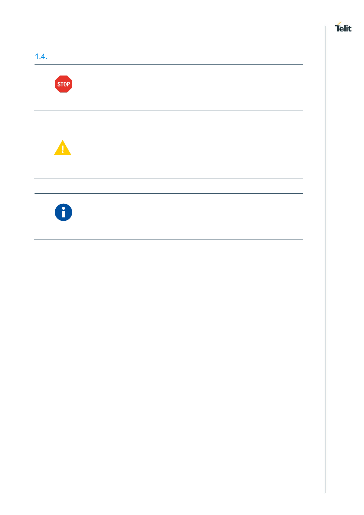
Danger – This information MUST be followed or catastrophic
equipment failure or bodily injury may occur.
Caution or Warning – Alerts the user to important points about
integrating the module, if these points are not followed, the module and
end user equipment may fail or malfunction.
Tip or Information – Provides advice and suggestions that may be
useful when integrating the module.
All dates are in ISO 8601 format, i.e. YYYY-MM-DD.

LE866 Hardware Design Guide
1VV0301355 Rev. 3 Page 11 of 90 2017-09-07
Related Documents
SIM Holder Design Guides, 80000NT10001A
LE866 AT Commands Reference Guide, 80471ST10691A
Telit EVK2 User Guide, 1vv0300704
xE866 Interfaces User Guide, 1vv0301260
LE866 Hardware Design Guide
1VV0301355 Rev. 3 Page 12 of 90 2017-09-07
2. GENERAL PRODUCT DESCRIPTION
Overview
LE866 is Telit’s new LTE series for IoT applications.
In its most basic use case, LE866 can be applied as a wireless communication front-end
for telematics products, offering mobile communication features to an external host CPU
through its interfaces.
Product Variants and Frequency Bands
All LE866 variants are single mode LTE.
Different bands combinations are available:
Product
2G Band (MHz)
3G Band (MHz)
4G Band (MHz)
Region
LE866-SV1
B4 (AWS1700)
B13 (700)
North America
Verizon
LE866A1-NA
B2 (1900)
B4 (AWS1700)
B12 (700)
North America
AT&T
LE866A1-KK
B3 (1800)
B8 (900)
Korea
KT
LE866A1-KS
B3 (1800)
B5 (850)
Korea
SKT
LE866A1-JS
B1 (2100)
B8 (900)
Japan
Softbank
Refer to Chapter 13 for details information about frequencies and bands.

LE866 Hardware Design Guide
1VV0301355 Rev. 3 Page 13 of 90 2017-09-07
Target market
LE866 can be used for telematics applications where tamper-resistance, confidentiality,
integrity, and authenticity of end-user information are required, for example:
Emergency call
Telematics services
Road pricing
Pay-as-you-drive insurance
Stolen vehicles tracking
Internet connectivity
Main features
Function
Features
Modem
Multi-RAT cellular modem for voice and data communication
o LTE FDD Cat1 (10/5Mbps DL/UL).
o Carrier aggregation is not supported
SMS support (text and PDU)
Alarm management
Real Time Clock
SIM phonebook
Internal IP stack
GNSS
Not supported
Digital audio
subsystem
PCM/I2S digital audio interface
Up to 16 kHz sample rate, 16 bit words
Interfaces
USB2.0 – USB port is typically used for:
o Flashing of firmware and module configuration
o Production testing
o AT command access
o Diagnostic monitoring and debugging
Peripheral Ports – UART
7 GPIOs
Antenna ports
LE866 Hardware Design Guide
1VV0301355 Rev. 3 Page 14 of 90 2017-09-07
TX Output Power
Band
Power class
LTE All Bands
Class 3 (0.2W)
RX Sensitivity
Below the 3GPP measurement conditions used to define the RX sensitity:
Technology
3GPP Compliance
4G LTE
Throughput >95% 10MHz Dual Receiver
Product
Band
Sensitivity (dBm)
LE866-SV1
LTE FDD B4
LTE FDD B13
-102.0
LE866A1-NA
LTE FDD B2
LTE FDD B4
LTE FDD B12
-102.0
LE866A1-KK
LTE FDD B3
LTE FDD B8
-102.0
LE866A1-JS
LTE FDD B1
LTE FDD B8
-102.0

LE866 Hardware Design Guide
1VV0301355 Rev. 3 Page 15 of 90 2017-09-07
Mechanical specifications
2.7.1. Dimensions
The overall dimensions of LE866 family are:
Length: 25 mm
Width: 15 mm
Thickness: 2.2 mm
2.7.2. Weight
The nominal weight of the module is 1.80 grams.
Temperature range
Note
Operating Temperature
Range
–20°C ÷ +55°C
The module is fully
functional(*) in all the
temperature range, and it
fully meets the 3GPP
specifications.
–40°C ÷ +85°C
The module is fully
functional (*) in all the
temperature range.
Storage and non-
operating Temperature
Range
–40°C ÷ +85°C
(*) Functional: the module is able to make and receive voice calls, data calls, SMS and
make data traffic.
LE866 Hardware Design Guide
1VV0301355 Rev. 3 Page 16 of 90 2017-09-07
3. PINS ALLOCATION
Pin-out
Pin
Signal
I/O
Function
Type
Comment
USB HS 2.0 COMMUNICATION PORT
E5
USB_D+
I/O
USB differential Data (+)
-
E6
USB_D-
I/O
USB differential Data (-)
-
Asynchronous Serial Port (USIF0) – Prog. / Data + HW Flow Control
A4
C103/TXD
I
Serial data input (TXD) from DTE
CMOS 1.8V
A5
C104/RXD
O
Serial data output to DTE
CMOS 1.8V
A2
C108/DTR
I
Input for (DTR) from DTE
CMOS 1.8V
A1
C105/RTS
I
Input for Request to send signal (RTS) from
DTE
CMOS 1.8V
B1
C106/CTS
O
Output for Clear to send signal (CTS) to
DTE
CMOS 1.8V
B2
C109/DCD
O
Output for (DCD) to DTE
CMOS 1.8V
A3
C107/DSR
O
Output for (DSR) to DTE
CMOS 1.8V
B3
C125/RING
O
Output for Ring (RI) to DTE
CMOS 1.8V
Asynchronous Auxiliary Serial Port (USIF1)
C1
TX_AUX
O
Auxiliary UART (TX Data to DTE)
CMOS 1.8V
C2
RX_AUX
I
Auxiliary UART (RX Data from DTE)
CMOS 1.8V
SIM card interface
C7
SIMVCC
-
External SIM signal – Power supply for the
SIM
1.8V Only
B7
SIMRST
O
External SIM signal – Reset
CMOS 1.8
A7
SIMCLK
O
External SIM signal – Clock
CMOS 1.8
LE866 Hardware Design Guide
1VV0301355 Rev. 3 Page 17 of 90 2017-09-07
A6
SIMIO
I/O
External SIM signal – Data I/O
CMOS 1.8
X
SIMIN
I
Presence SIM input
CMOS 1.8
See next chapters
DIGITAL IO
C5
GPIO_01
DVI_WA0
SIM_IN
I/O
INT
Main Function: GPIO01 Configurable GPIO
Alternate function 1: Digital Audio Interface
(WA0)
Alternate Function 2: SIM_IN
CMOS 1.8V
C6
GPIO_02
DVI_RX
SIM_IN
I/O
INT
Main Function: GPIO02 Configurable GPIO
Alternate Function 1: Digital Audio Interface
(RX)
Alternate Function 2: SIM_IN
CMOS 1.8V
D6
GPIO_03
DVI_TX
SIM_IN
I/O
INT
General Purpose IO
Alternate Function 1: Digital Audio Interface
(TX)
Alternate Function 2: SIM_IN
CMOS 1.8V
D5
GPIO_04
DVI_CLK
SIM_IN
I/O
INT
Main Function: GPIO04 Configurable GPIO
Alternate Function1: Digital Audio Interface
(CLK)
Alternate Function 2: SIM_IN
CMOS 1.8V
B5
GPIO_05
SIM_IN
I/O
INT
Main Function: GPIO05 Configurable GPIO
Alternate Function 1: SIM_IN
CMOS 1.8V
B4
GPIO_06
ALARM
SIM_IN
I/O
INT
Main Function: GPIO06 Configurable GPIO
Alternate Function 1: ALARM
Alternate Function 2: SIM_IN
CMOS 1.8V
C4
GPIO_07
STAT_LED
SIM_IN
I/O
INT
Main Function: GPIO07 Configurable GPIO
Alternate Function 1: STATLED
Alternate Function 2: SIM_IN
CMOS 1.8V
D8
VDDIO_IN
I
IO bus Supply input
Power
ADC and DAC
F4
ADC_IN1
AI
Analog/Digital converter input
A/D
Accepted values 0
to 1.0V DC
E4
DAC_OUT
AO
Digital/Analog converter output
D/A
RF Section
G2
MAIN_ANT
I/O
LTE Main Antenna (50 ohm)
RF
C0
DIV_ANT
I
LTE RX Diversity Antenna (50 ohm)
RF
LE866 Hardware Design Guide
1VV0301355 Rev. 3 Page 18 of 90 2017-09-07
Miscellaneous Functions
G4
RESET*
I
Reset Input
VBATT
Pull up to VBATT
(10Kohm)
G6
VAUX/PWRMON
O
1.8V stabilized output
Power ON monitor
Power
3GPP Rel12 PSM (Power Saving Mode)
D3
PSM_WAKE
I
3GPP Rel12 PSM Wake Up
Analog
E8
PSM_STATUS
O
3GPP Rel12 PSM Status
CMOS 1.8V
F8
PSM_ENA_OUT
O
3GPP Rel12 PSM Enable for external LDOs
CMOS 1.8V
Power Supply
E2
VBATT
-
Main power supply (Baseband)
Power
E0
VBATT_PA
-
Main power supply (Radio PA)
Power
E1
VBATT_PA
-
Main power supply (Radio PA)
Power
B0
GND
-
Ground
Power
D0
GND
-
Ground
Power
F0
GND
-
Ground
Power
G0
GND
-
Ground
Power
D1
GND
-
Ground
Power
F1
GND
-
Ground
Power
G1
GND
-
Ground
Power
D2
GND
-
Ground
Power
F2
GND
-
Ground
Power
C3
GND
-
Ground
Power
E3
GND
-
Ground
Power
LE866 Hardware Design Guide
1VV0301355 Rev. 3 Page 19 of 90 2017-09-07
F3
GND
-
Ground
Power
G3
GND
-
Ground
Power
F6
GND
-
Ground
Power
A8
GND
-
Ground
Power
G8
GND
-
Ground
Power
A11
GND
-
Ground
Power
G11
GND
-
Ground
Power
RESERVED
A0
RESERVED
-
RESERVED
G5
RESERVED
-
RESERVED
B6
RESERVED
-
RESERVED
D7
RESERVED
-
RESERVED
E7
RESERVED
-
RESERVED
F7
RESERVED
-
RESERVED
G7
RESERVED
-
RESERVED
B8
RESERVED
-
RESERVED
C8
RESERVED
-
RESERVED
A9
RESERVED
-
RESERVED
B9
RESERVED
-
RESERVED
C9
RESERVED
-
RESERVED
D9
RESERVED
-
RESERVED
E9
RESERVED
-
RESERVED
F9
RESERVED
-
RESERVED
LE866 Hardware Design Guide
1VV0301355 Rev. 3 Page 20 of 90 2017-09-07
WARNING
Reserved pins must not be connected.
G9
RESERVED
-
RESERVED
A10
RESERVED
-
RESERVED
B10
RESERVED
-
RESERVED
C10
RESERVED
-
RESERVED
D10
RESERVED
-
RESERVED
E10
RESERVED
-
RESERVED
F10
RESERVED
-
RESERVED
G10
RESERVED
-
RESERVED
B11
RESERVED
-
RESERVED
C11
RESERVED
-
RESERVED
D4
RESERVED
-
RESERVED
F5
RESERVED
-
RESERVED
F11
RESERVED
-
RESERVED
E11
RESERVED
-
RESERVED
D11
RESERVED
-
RESERVED

LE866 Hardware Design Guide
1VV0301355 Rev. 3 Page 21 of 90 2017-09-07
If not used, almost all pins should be left disconnected. The only exceptions are the
following pins:
Pad
Signal
Note
E2
VBATT
E0
VBATT_PA
E1
VBATT_PA
B0, D0, F0, G0, D1, F1, G1,
D2, F2, C3, E3, F3, G3, F6,
A8, G8, A11, G11
GND
G2
Main Antenna
C0
Diversity Antenna
A4
C103/TXD
If not used should be connected to a Test Point
A5
C104/RXD
If not used should be connected to a Test Point
A1
C105/RTS
If not used should be connected to a Test Point
B1
C106/CTS
If not used should be connected to a Test Point
G6
VAUX / PWRMON
G4
RESET*
C1
TXD_AUX
If not used should be connected to a Test Point
C2
RXD_AUX
If not used should be connected to a Test Point
E5
USB D+
If not used should be connected to a Test Point or an USB
connector
E6
USB D-
If not used should be connected to a Test Point or an USB
connector
C7
SIMVCC
B7
SIMRST

LE866 Hardware Design Guide
1VV0301355 Rev. 3 Page 22 of 90 2017-09-07
RTS pin should be connected to the GND (on the module side) if flow control is not used.
The above pins are also necessary to debug the application when the module is
assembled on it so we recommend connecting them also to dedicated test point.
A7
SIMCLK
A6
SIMIO
D8
VDDIO_IN
To be always supplied (or using VAUX/PWRMON or with an
external LDO)
LE866 Hardware Design Guide
1VV0301355 Rev. 3 Page 23 of 90 2017-09-07
LGA Pads Layout
TOP VIEW
A
B
C
D
E
F
G
0
RESERVED
GND
DIV
ANT
GND
VBATT_PA
GND
GND
1
C105/RTS
C106/CTS
TX AUX
GND
VBATT_PA
GND
GND
2
C108/DTR
C109/DCD
RX AUX
GND
VBATT
GND
MAIN
ANT
3
C107/DSR
C125/RING
GND
PSM_WAK
E
GND
GND
GND
4
C103/TXD
GPIO_06
GPIO_07
RESERVED
DAC_OUT
ADC_IN1
RESET*
5
C104/RXD
GPIO_05
GPIO_01
GPIO_04
USB_D+
RESERVED
RESERVED
6
SIMIO
RESERVED
GPIO_02
GPIO_03
USB_D-
GND
VAUX/PWR
MON
7
SIMCLK
SIMRST
SIMVCC
RESERVED
RESERVED
RESERVED
RESERVED
8
GND
RESERVED
RESERVED
VDDIO_IN
PSM_STAT
US
PSM_ENA_
OUT
GND
9
RESERVED
RESERVED
RESERVED
RESERVED
RESERVED
RESERVED
RESERVED
10
RESERVED
RESERVED
RESERVED
RESERVED
RESERVED
RESERVED
RESERVED
11
GND
RESERVED
RESERVED
RESERVED
RESERVED
RESERVED
GND
LE866 Hardware Design Guide
1VV0301355 Rev. 3 Page 24 of 90 2017-09-07
4. POWER SUPPLY
The power supply circuitry and board layout are a very important part in the full product
design and they strongly reflect on the product overall performances, hence read carefully
the requirements and the guidelines that will follow for a proper design.
Power Supply Requirements
The external power supply must be connected to VBATT & VBATT_PA signals and must
fulfil the following requirements:
Power Supply
Value
Nominal Supply Voltage
3.8V
Normal Operating Voltage Range
3.40 V÷ 4.20 V
Extended Operating Voltage Range
3.10 V÷ 4.50 V
NOTE:
The Operating Voltage Range MUST never be exceeded; care must
be taken when designing the application’s power supply section to
avoid having an excessive voltage drop.
If the voltage drop is exceeding the limits it could cause a Power Off
of the module.
Overshoot voltage (regarding MAX Extended Operating Voltage) and
drop in voltage (regarding MIN Extended Operating Voltage) MUST
never be exceeded;
The “Extended Operating Voltage Range” can be used only with
completely assumption and application of the HW User guide
suggestions.
LE866 Hardware Design Guide
1VV0301355 Rev. 3 Page 25 of 90 2017-09-07
Power Consumption
Mode
Average (mA)
Mode Description
AT+CFUN=1
23.4
Connected mode
USB Not connected
AT+CFUN=4
21.0
Radio Disabled
USB Not connected
AT+CFUN=5
3.0
Power Saving Enabled
USB not connected
I-DRX (3GPP Rel.8) – paging
2.56s
LTE Data Call (Min Power)
395
LTE data call (channel BW 5MHz,
RB=1, TX=0dBm)
LTE Data Call (Max Power)
580
LTE data call (channel BW 5MHz,
RB=1, TX=22dBm)
NOTE:
The electrical design for the Power supply should be made ensuring
it will be capable of a peak current output of at least 1 A.

LE866 Hardware Design Guide
1VV0301355 Rev. 3 Page 26 of 90 2017-09-07
General Design Rules
The principal guidelines for the Power Supply Design embrace three different design
steps:
the electrical design
the thermal design
the PCB layout.
4.3.1. Electrical Design Guidelines
The electrical design of the power supply depends strongly from the power source where
this power is drained. We will distinguish them into three categories:
+5V input (typically PC internal regulator output)
+12V input (typically automotive)
Battery
4.3.1.1. +5V Source Power Supply Design Guidelines
The desired output for the power supply is 3.8V, hence there’s not a big difference
between the input source and the desired output and a linear regulator can be used.
A switching power supply will not be suited because of the low drop out
requirements.
When using a linear regulator, a proper heat sink shall be provided in order to
dissipate the power generated.
A Bypass low ESR capacitor of adequate capacity must be provided in order to cut
the current absorption peaks close to the Module, a 100μF capacitor is usually
suited.
Make sure the low ESR capacitor on the power supply output rated at least 10V.
An example of linear regulator with 5V input is:
LE866 Hardware Design Guide
1VV0301355 Rev. 3 Page 27 of 90 2017-09-07
LE866 Hardware Design Guide
1VV0301355 Rev. 3 Page 28 of 90 2017-09-07
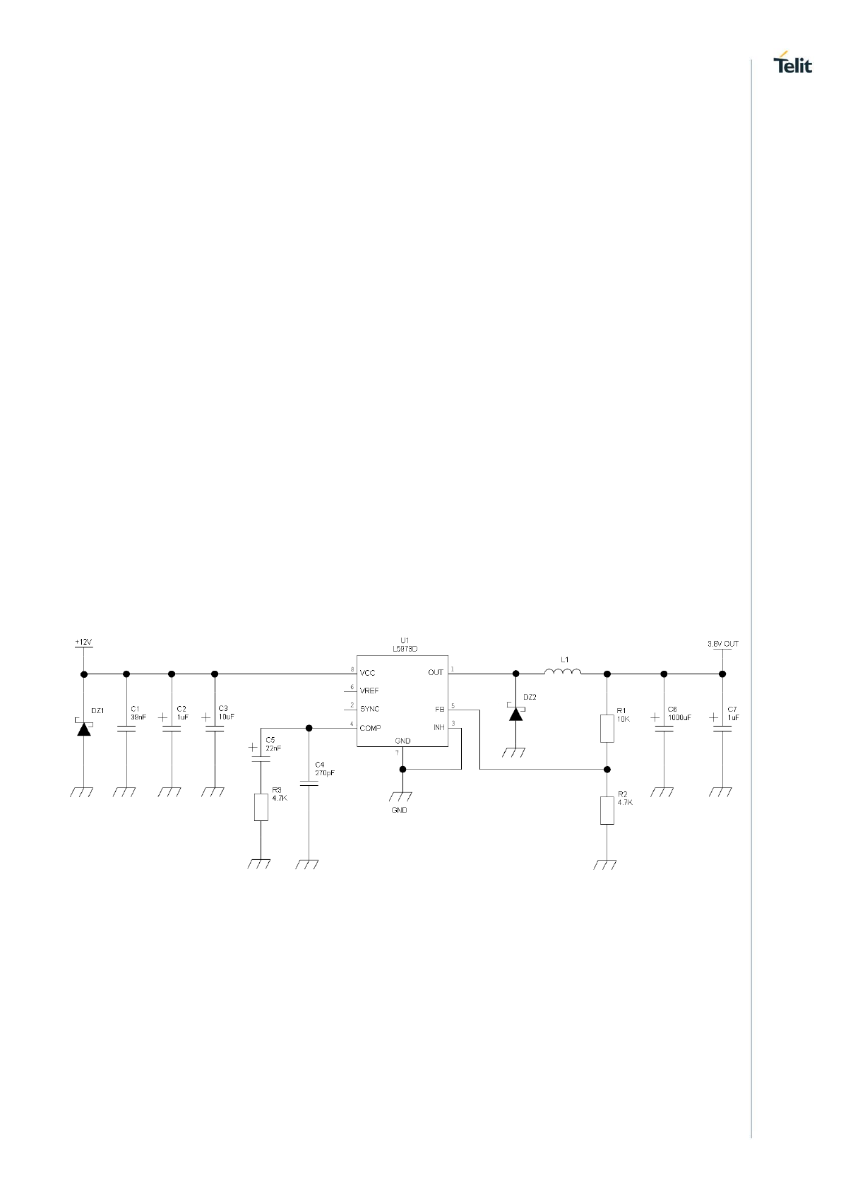
4.3.2. +12V Source Power Supply Design Guidelines
The desired output for the power supply is 3.8V, hence due to the big difference
between the input source and the desired output, a linear regulator is not suited and
shall not be used. A switching power supply will be preferable because of its better
efficiency.
When using a switching regulator, a 500kHz or more switching frequency regulator
is preferable because of its smaller inductor size and its faster transient response.
This allows the regulator to respond quickly to the current peaks absorption.
In any case the frequency and Switching design selection is related to the
application to be developed due to the fact the switching frequency could also
generate EMC interferences.
For car PB battery the input voltage can rise up to 15,8V and this should be kept in
mind when choosing components: all components in the power supply must
withstand this voltage.
A Bypass low ESR capacitor of adequate capacity must be provided in order to cut
the current absorption peaks, a 100μF capacitor is usually suited.
Make sure the low ESR capacitor on the power supply output is rated at least 10V.
For Car applications a spike protection diode should be inserted close to the power
input, in order to clean the supply from spikes.
An example of switching regulator with 12V input is in the below schematic:
LE866 Hardware Design Guide
1VV0301355 Rev. 3 Page 29 of 90 2017-09-07
4.3.2.1. Battery Source Power Supply Design Guidelines
The desired nominal output for the power supply is 3.8V and the maximum voltage allowed
is 4.2V, hence a single 3.7V Li-Ion cell battery type is suited for supplying the power to the
Telit LE866 module.
A Bypass low ESR capacitor of adequate capacity must be provided in order to cut
the current absorption peaks, a 100μF tantalum capacitor is usually suited.
Make sure the low ESR capacitor (usually a tantalum one) is rated at least 10V.
A protection diode should be inserted close to the power input, in order to save the
LE866 from power polarity inversion. Otherwise the battery connector should be
done in a way to avoid polarity inversions when connecting the battery.
The battery capacity must be at least 500mAh in order to withstand the current
peaks of 2A; the suggested capacity is from 500mAh to 1000mAh.
WARNING:
The three cells Ni/Cd or Ni/MH 3,6 V Nom. Battery types or 4V PB
types MUST NOT BE USED DIRECTLY since their maximum voltage
can rise over the absolute maximum voltage for the LE866 and
damage it.
NOTE:
DON’T USE any Ni-Cd, Ni-MH, and Pb battery types directly
connected with LE866. Their use can lead to overvoltage on the
LE866 and damage it. USE ONLY Li-Ion battery types.

LE866 Hardware Design Guide
1VV0301355 Rev. 3 Page 30 of 90 2017-09-07
4.3.3. Thermal Design Guidelines
The thermal design for the power supply heat sink should be done with the following
specifications:
Average current consumption during LTE transmission @PWR level max : 600
mA
Average current during idle: 23 mA
Considering the very low current during idle, especially if Power Saving function is enabled,
it is possible to consider from the thermal point of view that the device absorbs current
significantly only during calls.
If we assume that the device stays into transmission for short periods of time (let’s say few
minutes) and then remains for a quite long time in idle (let’s say one hour), then the power
supply has always the time to cool down between the calls and the heat sink could be
smaller than the calculated one for 700mA maximum RMS current, or even could be the
simple chip package (no heat sink).
Moreover in the average network conditions the device is requested to transmit at a lower
power level than the maximum and hence the current consumption will be less than the
700mA, being usually around 150mA.
For these reasons the thermal design is rarely a concern and the simple ground plane where
the power supply chip is placed can be enough to ensure a good thermal condition and
avoid overheating.
The generated heat will be mostly conducted to the ground plane under the LE866; you
must ensure that your application can dissipate it.
NOTE:
The average consumption during transmissions depends on the
power level at which the device is requested to transmit by the
network. The average current consumption hence varies significantly.

LE866 Hardware Design Guide
1VV0301355 Rev. 3 Page 31 of 90 2017-09-07
4.3.4. Power Supply PCB layout Guidelines
As seen on the electrical design guidelines the power supply shall have a low ESR capacitor
on the output to cut the current peaks on the input to protect the supply from spikes The
placement of this component is crucial for the correct working of the circuitry. A misplaced
component can be useless or can even decrease the power supply performances.
The Bypass low ESR capacitor must be placed close to the Telit LE866 power input
pads or in the case the power supply is a switching type it can be placed close to
the inductor to cut the ripple provided the PCB trace from the capacitor to the LE866
is wide enough to ensure a dropless connection even during an 1A current peak.
The protection diode must be placed close to the input connector where the power
source is drained.
The PCB traces from the input connector to the power regulator IC must be wide
enough to ensure no voltage drops occur when an 1A current peak is absorbed.
The PCB traces to the LE866 and the Bypass capacitor must be wide enough to
ensure no significant voltage drops occur. This is for the same reason as previous
point. Try to keep this trace as short as possible.
To reduce the EMI due to switching, it is important to keep very small the mesh
involved; thus the input capacitor, the output diode (if not embodied in the IC) and
the regulator have to form a very small loop.This is done in order to reduce the
radiated field (noise) at the switching frequency (100-500 kHz usually).
A dedicated ground for the Switching regulator separated by the common ground
plane is suggested.
The placement of the power supply on the board should be done in such a way to
guarantee that the high current return paths in the ground plane are not overlapped
to any noise sensitive circuitry as the microphone amplifier/buffer or earphone
amplifier.
The power supply input cables should be kept separate from noise sensitive lines
such as microphone/earphone cables.
The insertion of EMI filter on VBATT pins is suggested in those designs where
antenna is placed close to battery or supply lines.
A ferrite bead like Murata BLM18EG101TN1 or Taiyo Yuden P/N
FBMH1608HM101 can be used for this purpose.

LE866 Hardware Design Guide
1VV0301355 Rev. 3 Page 32 of 90 2017-09-07
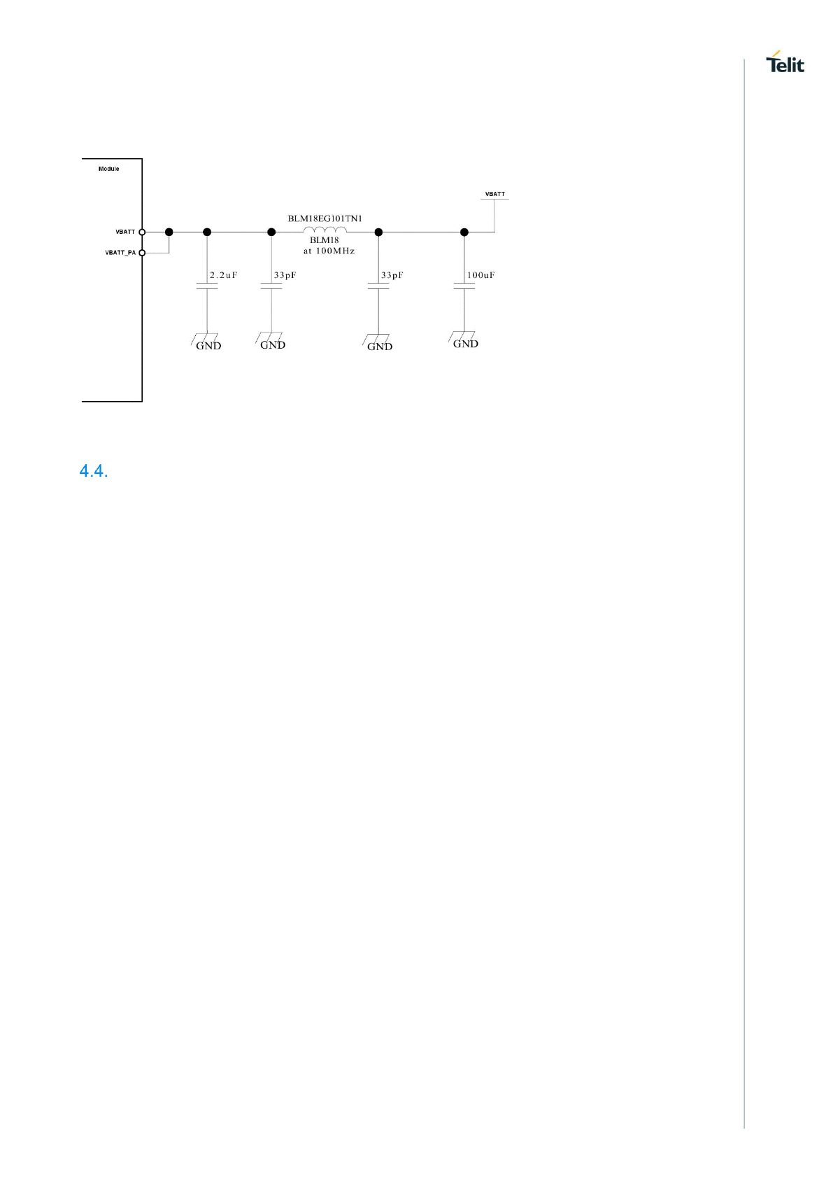
LE866 Hardware Design Guide
1VV0301355 Rev. 3 Page 33 of 90 2017-09-07
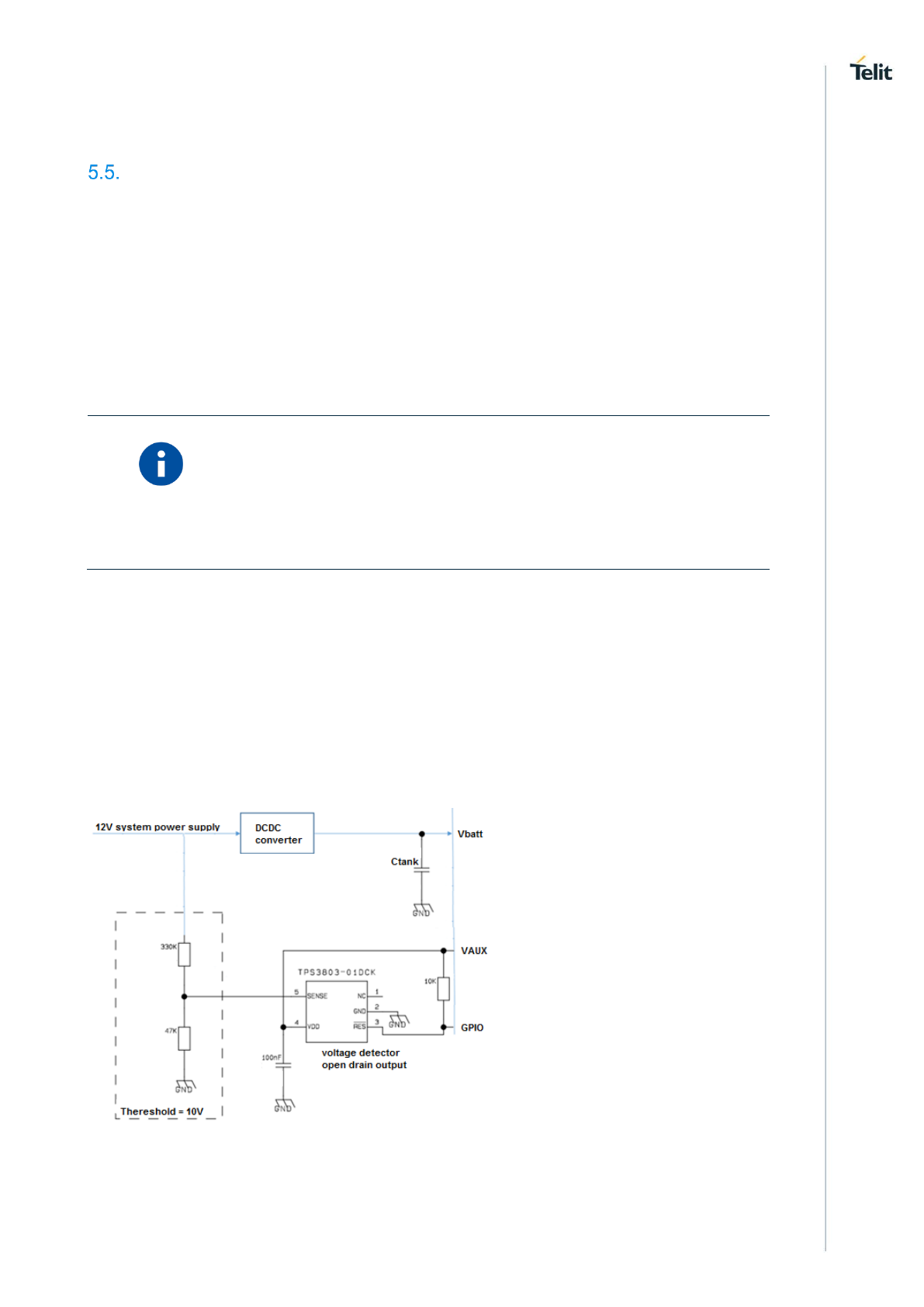
The below figure shows the recommended circuit:
RTC Bypass out
The LE866 module is provided by an internal RTC section but its reference supply is
VBATT.
So, in order to maintain active the RTC programming, VBATT should not be removed
LE866 Hardware Design Guide
1VV0301355 Rev. 3 Page 34 of 90 2017-09-07
VAUX Power Output
A regulated power supply output is provided in order to supply small devices from the
module. The signal is present on Pad G6 and it is in common with the PWRMON (module
powered ON indication) function.
This output is always active when the module is powered ON.
The operating range characteristics of the supply are:
Item
Min
Typical
Max
Output voltage
1.7V
1.80V
1.9V
Output current
-
-
60mA
Output bypass capacitor
1.7V
1uF
NOTE:
The Output Current MUST never be exceeded; care must be taken
when designing the application section to avoid having an excessive
current consumption.
If the Current is exceeding the limits it could cause a Power Off of the
module.
NOTE:
VAUX is switched OFF when the module enters in PSM mode
(AT#PSM=2)
Warning:
The current consumption from VAUX_PWRMON increases the
modem temperature.
LE866 Hardware Design Guide
1VV0301355 Rev. 3 Page 35 of 90 2017-09-07
VDDIO_IN Power Input
VDDIO_IN is an input line used to supply the Digital section of LE866.
The operating range characteristics of the external supply have to be:
Item
Min
Typical
Max
Voltage
1.7V
1.80V
1.9V
NOTE:
If VDDIO_IN line is not powered (i.e. during the sleep states in
PSM=2 when supplied by VAUX, during transition phases BOOT,
RESET etc. and when the module is unsupplied) it is important to
avoid back powering the digital pins.
Exceeding the absolute maximum ratings could damage permanently
the module.
NOTE:
VDDIO_IN can be directly supplied from VAUX_PWRMON line
(adding an R0 in series for debug purposes).
LE866 Hardware Design Guide
1VV0301355 Rev. 3 Page 36 of 90 2017-09-07
3GPP Power Saving Mode (PSM)
The LE866 is supporting a new feature introduced in 3GPP Rel.12 that allows the Module
to skip idle mode tasks for a longer time period while still maintaining the NAS context.
This feature permits to reduce the overall power consumption when there is no required
data activity with the network for a long time.
Additional hardware lines are defined to support this feature and to synchronize the
activities with the external Host processor.
Signal
Function
I/O
Pad
VDDIO_IN
IO bus Supply input
I
D8
PSM_WAKE
PSM Wake Up
I
D3
PSM_STATUS
PSM Status indication
O
E8
PSM_ENA_OUT
PSM Enable for external LDOs
O
F8
A detailed description of the PSM use and design examples is available in the LE866
PSM Application Note.
NOTE:
If VDDIO_IN line is not powered (i.e. during the sleep states in
PSM=2 when supplied by VAUX, during transition phases BOOT,
RESET etc. and when the module is unsupplied) it is important to
avoid back powering the digital pins.
Exceeding the absolute maximum ratings could damage permanently
the module.
LE866 Hardware Design Guide
1VV0301355 Rev. 3 Page 37 of 90 2017-09-07
5. DIGITAL SECTION
Logic Levels
ABSOLUTE MAXIMUM RATINGS:
Parameter
Min
Max
Input level on any digital pin (CMOS 1.8) with respect
to ground
-0.3V
VDDIO_IN
+0.3V
Input level on any digital pin (CMOS 1.8) with respect
to ground
OPERATING RANGE – INTERFACE LEVELS (1.8V CMOS):
Parameter
Min
Max
Input high level
1.55V
1.9V
Input low level
0V
0.35V
Output high level
1.35V
1.8V
Output low level
0V
0.8V
CURRENT CHARACTERISTICS:
Parameter
AVG
Input Current
10uA
LE866 Hardware Design Guide
1VV0301355 Rev. 3 Page 38 of 90 2017-09-07
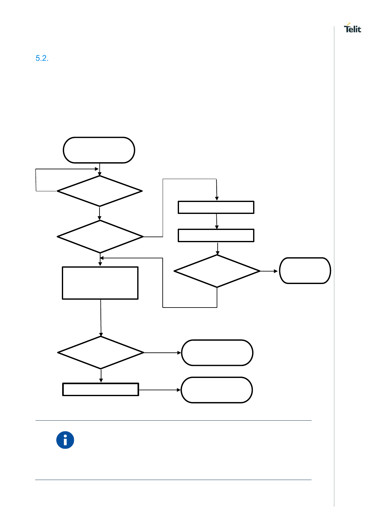
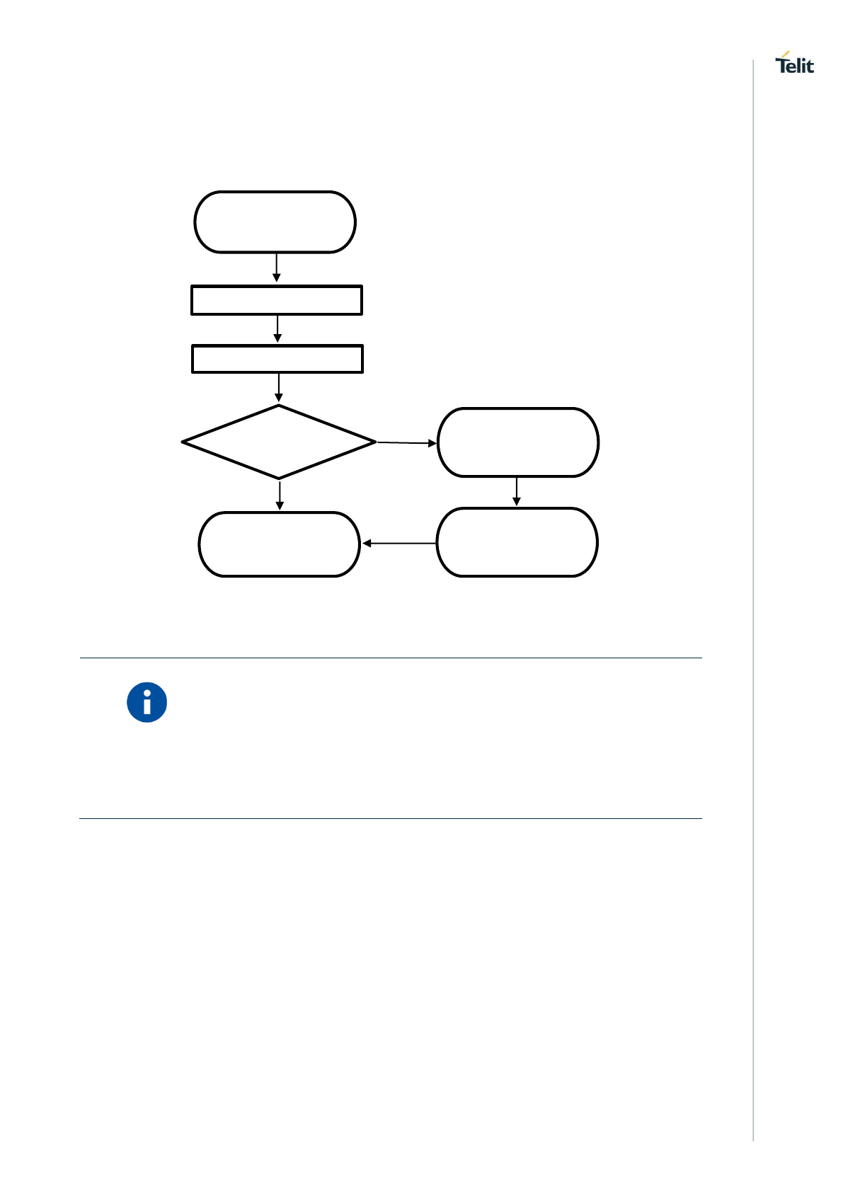
Power On
The LE866 will automatically power on itself when VBATT & VBATT_PA are applied to the
module.
VAUX / PWRMON pin will be then set at the high logic level.
The following flow chart shows the proper turn on procedure:
NOTE:
The power supply must be applied either at the same time on pins
VBATT and VBATT_PA.
PWRMON=ON ?
“Modem ON Proc”
START
PWRMON=ON ?
Delay = 25 s
AT Init Sequence
Enter AT<CR>
N
Delay 1s – 5s for Low Voltage
Operating
Y
Y
N
Y
Delay = 25 sec
N
Start AT CMD
AT Answer in
1sec?
Modem Reset Proc
N
Y
PWR Supply ON
LE866 Hardware Design Guide
1VV0301355 Rev. 3 Page 39 of 90 2017-09-07
A flow chart showing the AT commands managing procedure is displayed below:
NOTE:
In order to avoid a back powering effect it is recommended to avoid
having any HIGH logic level signal applied to the digital pins of the
LE866 when the module is not supplied or during a reboot transition.
“Start AT CMD”
START
Delay = 300 msec
Enter AT <CR>
Disconnect PWR Supply
AT answer in
1 sec ?
GO TO
“Modem ON Proc.”
“Start AT CMD”
END
Y
N
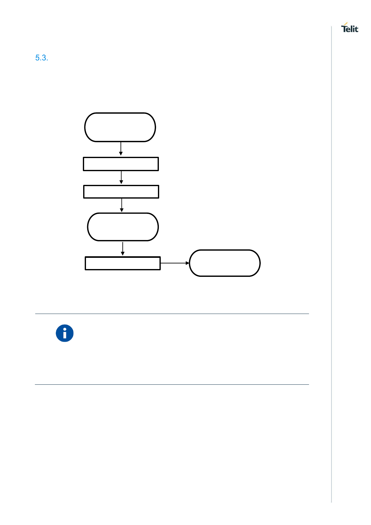
LE866 Hardware Design Guide
1VV0301355 Rev. 3 Page 40 of 90 2017-09-07
Power Off
The following flowchart shows the proper Turn-off procedure:
In order to avoid a back powering effect it is recommended to avoid
having any HIGH logic level signal applied to the digital pins of the
LE866 when the module is powered off or during an ON/OFF
transition.
“Modem OFF Proc”
AT#SYSHALT
10s Timeout
Disconnect PWR Supply
“Modem ON Proc.”
Delay 1.5s

LE866 Hardware Design Guide
1VV0301355 Rev. 3 Page 41 of 90 2017-09-07
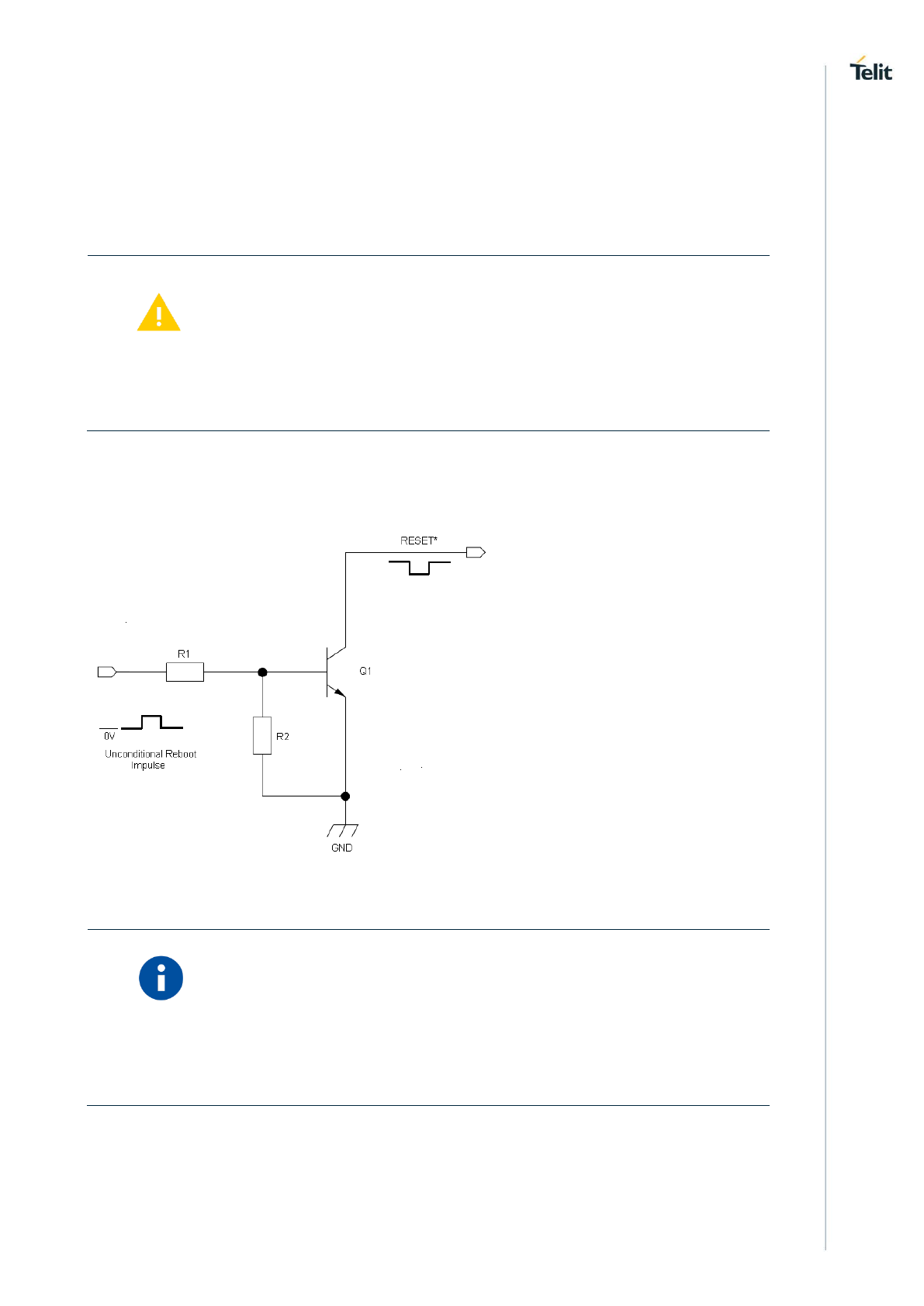
Unconditional Restart
To unconditionally restart the LE866, the pad RESET* must be tied low for at least 200
milliseconds and then released.
The maximum current that can be drained from the RESET* pad is 0,15 mA.
The hardware unconditional Restart must not be used during normal operation of the
device since it does not detach the device from the network. It shall be kept as an
emergency exit procedure to be done in the rare case that the device gets stuck waiting
for some network or SIM responses.
Do not use any pull up resistor on the RESET* line nor any totem pole digital output.
Using pull up resistor may bring to latch up problems on the LE866 power regulator and
improper functioning of the module.
The line RESET* must be connected only in open collector configuration; the transistor
must be connected as close as possible to the RESET* pin.
The unconditional hardware restart must always be implemented on the boards and the
software must use it as an emergency exit procedure.
PIN DESCRIPTION
Signal
Function
I/O
Pad
RESET*
Unconditional Reset of the Module
I
G4
LE866 Hardware Design Guide
1VV0301355 Rev. 3 Page 42 of 90 2017-09-07
OPERATING LEVELS
The RESET* line is connected to VBATT with a Pull Up so the electrical levels are on this
pin are aligned to the main supply level.
WARNING:
The hardware unconditional Reset must not be used during normal
operation of the device since it does not detach the device from the
network. It shall be kept as an emergency exit procedure.
A typical circuit is the following:
NOTE:
In order to avoid a back powering effect it is recommended to avoid
having any HIGH logic level signal applied to the digital pins of the
LE866 when the module is powered off or during a reboot transition.
LE866 Hardware Design Guide
1VV0301355 Rev. 3 Page 43 of 90 2017-09-07
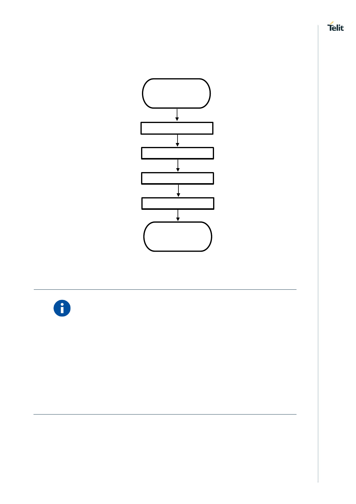
In the following flow chart is detailed the proper restart procedure:
NOTE:
Do not use any pull up resistor on the RESET* line nor any totem
pole digital output. Using pull up resistor may bring to latch up
problems on the LE866 power regulator and improper functioning of
the module.
To proper power on again the module please refer to the related
paragraph (“Power ON”)
The unconditional hardware reboot must always be implemented on
the boards and should be used only as an emergency exit procedure.
Modem RESET
Proc.
RESET* = LOW
Delay = 200ms
Start At CMD
RESET* = HIGH
Delay = 38s
LE866 Hardware Design Guide
1VV0301355 Rev. 3 Page 44 of 90 2017-09-07
Fast System Turn Off
The procedure to power off LE866 described in previous chapters normally takes more
than 1 second to detach from network and make LE866 internal filesystem properly
closed.
In case of unwanted supply voltage loss the system can be switched off without any risk of
filesystem data corruption by implementing Fast Syshalt feature.
Fast Syshalt feature permits to reduce the current consumption and the time-to-poweroff
to minimum values.
NOTE:
Refer to LE866 series AT command reference guide (Fast System
Turn-Off - #FASTSYSHALT) in order to set up detailed AT command.
5.5.1. Fast Turn Off by Hardware
The Fast System Turn Off can be triggered by configuration of any GPIO. HI level to LOW
level transition of GPIO commands fast SysHalt.
Example circuit:
LE866 Hardware Design Guide
1VV0301355 Rev. 3 Page 45 of 90 2017-09-07
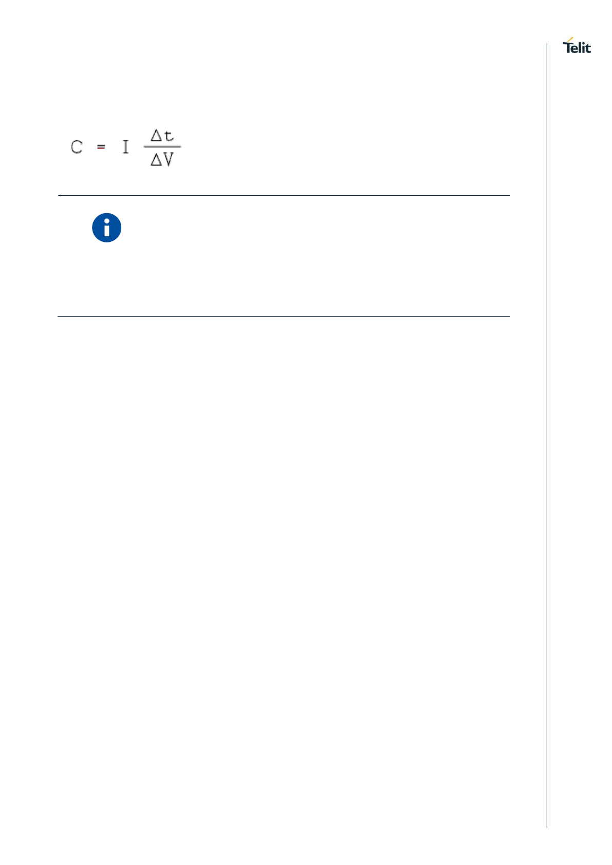
The capacitor is rated with the following formula:
NOTE:
In case of power on with slow ramp-up of Vbatt supply voltage,
RESET* line has to be used according to Power On diagram
described in previous chapters.
5.5.2. Fast Shut Down by Software
The Fast Power Down can be triggered by AT command.
LE866 Hardware Design Guide
1VV0301355 Rev. 3 Page 46 of 90 2017-09-07
Communication ports
5.6.1. USB 2.0 HS
The LE866 includes one integrated universal serial bus (USB 2.0 HS) transceiver.
The following table is listing the available signals:
PAD
Signal
I/O
Function
Type
E5
USB_D+
I/O
USB differential Data (+)
3.3V/100mV
E6
USB_D-
I/O
USB differential Data (-)
3.3V/100mV
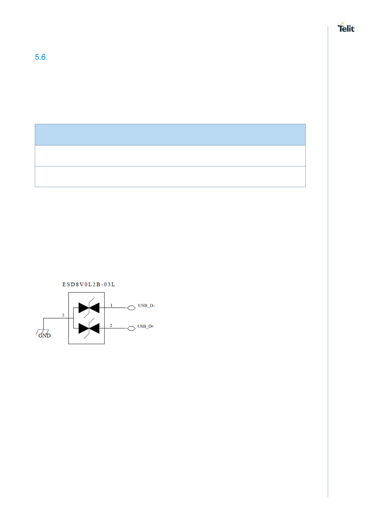
The USB_DPLUS and USB_DMINUS signals have a clock rate of 480 MHz.
The signal traces should be routed carefully. Trace lengths, number of vias and capacitive
loading should be minimized. The characteristic impedance value should be as close as
possible to 90 Ohms differential.
In case there is a need to add an ESD protection, the suggested connection is the
following:

LE866 Hardware Design Guide
1VV0301355 Rev. 3 Page 47 of 90 2017-09-07
5.6.2. Serial Ports
The LE866 module is provided with by 2 Asynchronous serial ports:
MODEM SERIAL PORT 1 (Main)
MODEM SERIAL PORT 2 (Auxiliary)
Several configurations can be designed for the serial port on the OEM hardware, but the
most common are:
RS232 PC com port
microcontroller UART @ 1.8V (Universal Asynchronous Receive Transmit)
microcontroller UART @ 5V or other voltages different from 1.8V
Depending from the type of serial port on the OEM hardware a level translator circuit may
be needed to make the system work.
On the LE866 the ports are CMOS 1.8.
5.6.2.1. MODEM SERIAL PORT 1 (USIF0)
The serial port 1 on the LE866 is a +1.8V UART with all the 7 RS232 signals.
It differs from the PC-RS232 in the signal polarity (RS232 is reversed) and levels.
The following table is listing the available signals:
RS232 pin
Signal
PAD
Name
Usage
1
C109/DCD
B2
Data Carrier Detect
Output from the LE866 that indicates
the carrier presence
2
C104/RXD
A5
Transmit line *see Note
Output transmit line of LE866 UART
3
C103/TXD
A4
Receive line *see Note
Input receive of the LE866 UART
4
C108/DTR
A2
Data Terminal Ready
Input to the LE866 that controls the
DTE READY condition
5
GND
D1, F1, G1,
D2, F2, C3,
E3, F3, G3,
F6, A8, G8,
A11, G11
Ground
Ground
6
C107/DSR
A2
Data Set Ready
Output from the LE866 that indicates
the module is ready
7
C106/CTS
A1
Clear to Send
Output from the LE866 that controls
the Hardware flow control
LE866 Hardware Design Guide
1VV0301355 Rev. 3 Page 48 of 90 2017-09-07
8
C105/RTS
B1
Request to Send
Input to the LE866 that controls the
Hardware flow control
9
C125/RING
B3
Ring Indicator
Output from the LE866 that indicates
the incoming call condition
NOTE:
According to V.24, some signal names are referred to the application
side, therefore on the LE866 side these signal are on the opposite
direction:
TXD on the application side will be connected to the receive line
(here named C103/TXD)
RXD on the application side will be connected to the transmit line
(here named C104/RXD)
For a minimum implementation, only the TXD, RXD lines can be
connected, the other lines can be left open provided a software flow
control is implemented.
In order to avoid a back powering effect it is recommended to avoid
having any HIGH logic level signal applied to the digital pins of the
LE866 when the module is powered off or during a reboot transition.
LE866 Hardware Design Guide
1VV0301355 Rev. 3 Page 49 of 90 2017-09-07
5.6.2.2. MODEM SERIAL PORT 2 (USIF1)
The secondary serial port on the LE866 is a CMOS1.8V with only the RX and TX signals.
The signals of the LE866 serial port are:
PAD
Signal
I/O
Function
Type
C1
TX_AUX
O
Auxiliary UART (TX Data to DTE)
CMOS 1.8V
C2
RX_AUX
I
Auxiliary UART (RX Data from DTE)
CMOS 1.8V
NOTE:
In order to avoid a back powering effect it is recommended to avoid
having any HIGH logic level signal applied to the digital pins of the
LE866 when the module is not supplied or during a reboot transition.
5.6.2.3. RS232 LEVEL TRANSLATION
In order to interface the LE866 with a PC com port or a RS232 (EIA/TIA-232) application a
level translator is required. This level translator must:
invert the electrical signal in both directions;
Change the level from 0/1.8V to +15/-15V.
Actually, the RS232 UART 16450, 16550, 16650 & 16750 chipsets accept signals with lower
levels on the RS232 side (EIA/TIA-562), allowing a lower voltage-multiplying ratio on the
level translator. Note that the negative signal voltage must be less than 0V and hence some
sort of level translation is always required.
The simplest way to translate the levels and invert the signal is by using a single chip level
translator. There are a multitude of them, differing in the number of drivers and receivers
and in the levels (be sure to get a true RS232 level translator not a RS485 or other
standards).
By convention the driver is the level translator from the 0-1.8V UART to the RS232 level.
The receiver is the translator from the RS232 level to 0-1.8V UART.
LE866 Hardware Design Guide
1VV0301355 Rev. 3 Page 50 of 90 2017-09-07
In order to translate the whole set of control lines of the UART you will need:
5 drivers
3 receivers
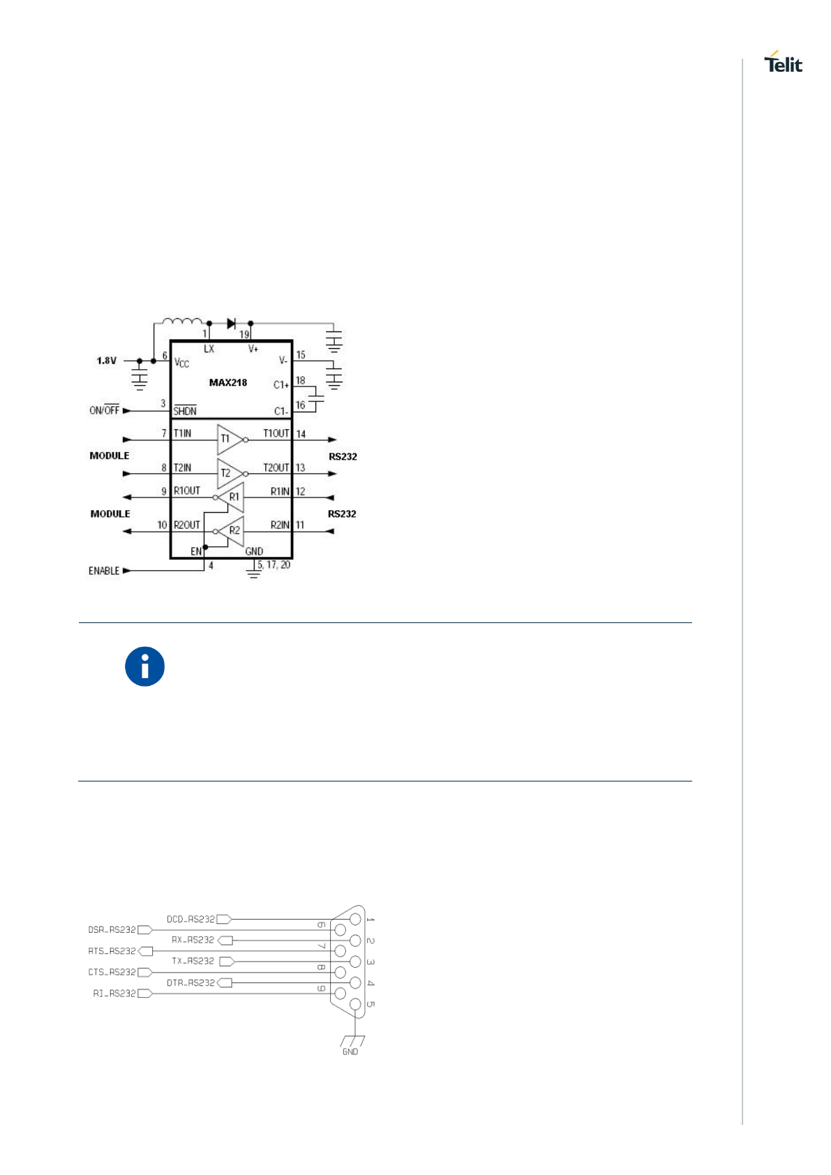
An example of RS232 level adaptation circuitry could be done using a MAXIM transceiver
(MAX218). In this case the chipset is capable to translate directly from 1.8V to the RS232
levels (Example done on 4 signals only).
NOTE:
Ensure to have the translator’s supply/enable synchronized with
VDDIO_IN supply source. The preferred configuration is having it
supplied from the same source used for VDDIO_IN.
The RS232 serial port lines are usually connected to a DB9 connector with the following
layout:
LE866 Hardware Design Guide
1VV0301355 Rev. 3 Page 51 of 90 2017-09-07
General purpose I/O
The LE866 module is provided by a set of Configurable Digital Input / Output pins (CMOS
1.8V)
Input pads can only be read; they report the digital value (high or low) present on the pad
at the read time.
Output pads can only be written or queried and set the value of the pad output.
An alternate function pad is internally controlled by the LE866 firmware and acts
depending on the function implemented.
The following table shows the available GPIO on the LE866:
PAD
Signal
I/O
Default State
Note
C5
GPIO_01
I/O
INPUT
Alternate functions:
Digital Audio Interface (WA0
C6
GPIO_02
I/O
INPUT
Alternate functions:
Digital Audio Interface (RX)
D6
GPIO_03
I/O
INPUT
Alternate functions:
Digital Audio Interface (TX)
D5
GPIO_04
I/O
INPUT
Alternate functions:
Digital Audio Interface (CLK)
B5
GPIO_05
I/O
INPUT
B4
GPIO_06
I/O
INPUT
Alternate functions:
ALARM
C4
GPIO_07
I/O
INPUT
Alternate functions:
STAT LED
LE866 Hardware Design Guide
1VV0301355 Rev. 3 Page 52 of 90 2017-09-07
NOTE:
The internal GPIO’s pull up/pull down could be set to the preferred
status for the application using the AT#GPIO command.
Please refer for the AT Commands User Guide for the detailed
command Syntax.
WARNING:
During power up the GPIOs may be subject to transient glitches.
5.7.1. Using a GPIO as INPUT
The GPIO pads, when used as inputs, can be connected to a digital output of another
device and report its status, provided this device has interface levels compatible with the
1.8V CMOS levels of the GPIO. If the digital output of the device to be connected with the
GPIO input pad has interface levels different from the 1.8V CMOS, then it can be buffered
with an open collector transistor with a 47K pull up to VAUX.
NOTE:
In order to avoid a back powering effect it is recommended to avoid
having any HIGH logic level signal applied to the digital pins of the
LE866 when the module is powered off or during a reboot transition.
The VAUX _PWRMON pin can be used for input pull up reference
or/and for ON monitoring.
LE866 Hardware Design Guide
1VV0301355 Rev. 3 Page 53 of 90 2017-09-07
5.7.2. Using a GPIO as OUTPUT
The GPIO pads, when used as outputs, can drive 1.8V CMOS digital devices or
compatible hardware. When set as outputs, the pads have a push-pull output and
therefore the pull-up resistor may be omitted.
5.7.3. Indication of network service availability
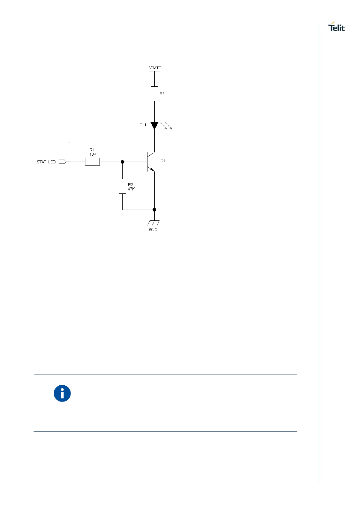
The STAT_LED pin status shows information on the network service availability and Call
status. The function is available as alternate function of GPIO_07 (to be enabled using the
AT#GPIO=7,0,2 command).
In the LE866 modules, the STAT_LED needs an external transistor to drive an external
LED. Therefore, the status indicated in the following table is reversed with respect to the
pin status.
Device Status
Led Status
Device off
Permanently off
Not Registered
Permanently on
Registered in idle
Blinking 1sec on + 2 sec off
Registered in idle + power saving
It depends on the event that triggers the
wakeup (In sync with network paging)
Voice Call Active
Permanently on
Dial-Up
Blinking 1 sec on + 2 sec off
LE866 Hardware Design Guide
1VV0301355 Rev. 3 Page 54 of 90 2017-09-07
A schematic example could be:
5.7.4. SIMIN Detection
All the GPIO pins can be used as SIM DETECT input. The AT Command used to enable
the function is:
AT#SIMINCFG
Use the AT command AT#SIMDET=2 to enable the SIMIN detection
Use the AT command AT&W0 and AT&P0 to store the SIMIN detection in the common
profile.
NOTE:
Don’t use the SIM IN function on the same pin where the GPIO
function is enabled and viceversa.
LE866 Hardware Design Guide
1VV0301355 Rev. 3 Page 55 of 90 2017-09-07
External SIM Holder
Please refer to the related User Guide (SIM Holder Design Guides, 80000NT10001a).
ADC Converter
The LE866 is provided by one AD converter. It is able to read a voltage level in the range
of 0÷1.2 volts applied on the ADC pin input, store and convert it into 10 bit word.
The input line is named as ADC_IN1 and it is available on Pad F4
The following table is showing the ADC characteristics:
Item
Min
Typical
Max
Unit
Input Voltage range
0
-
1.0
Volt
AD conversion
-
-
10
bits
The ADC could be controlled using an AT command.
The command is AT#ADC=1,2
The read value is expressed in mV
Refer to SW User Guide or AT Commands Reference Guide for the full description of this
function.
LE866 Hardware Design Guide
1VV0301355 Rev. 3 Page 56 of 90 2017-09-07
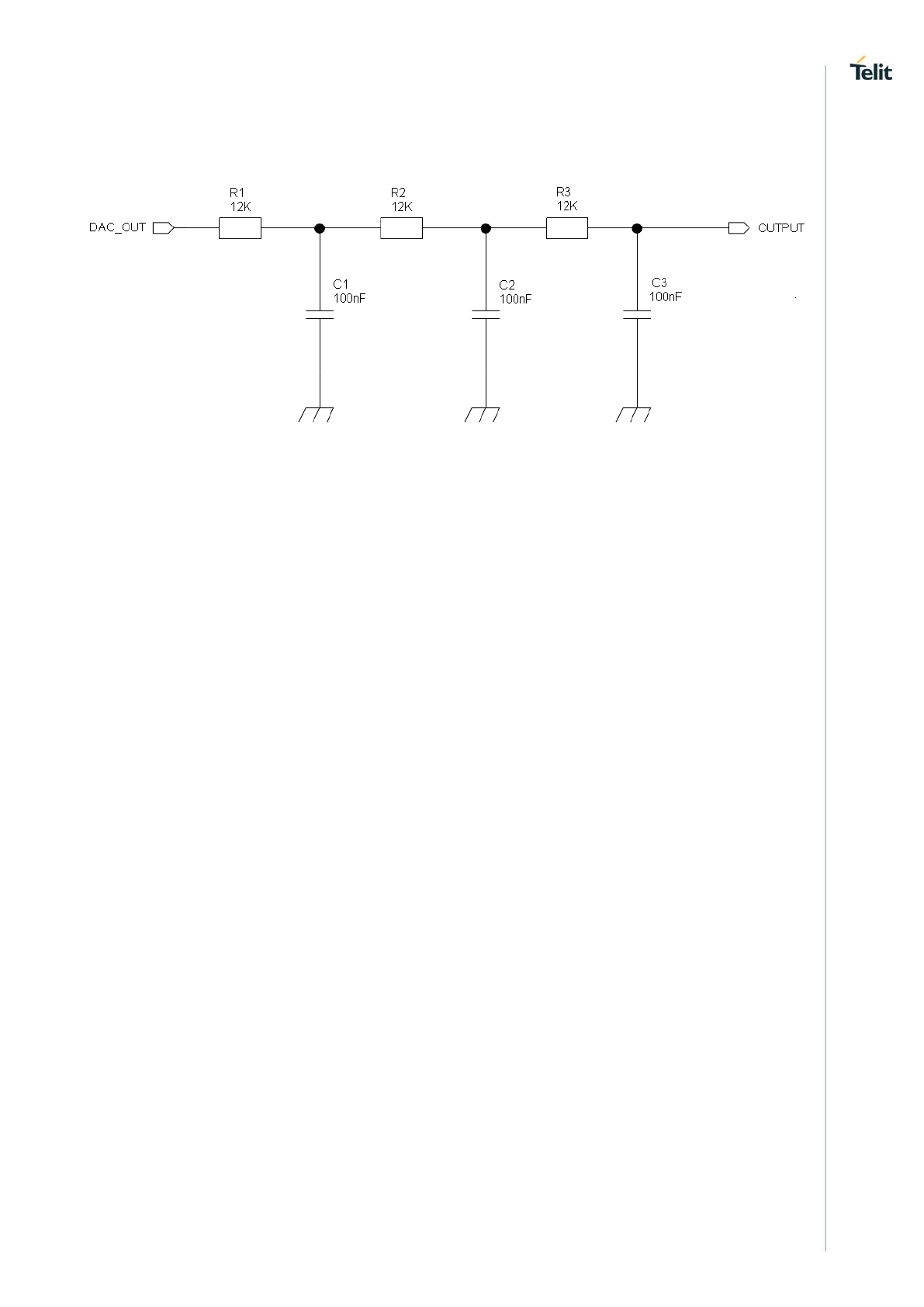
DAC Converter
The LE866 provides a Digital to Analog Converter. The signal (named DAC_OUT) is
available on pin E4 of the LE866. The on board DAC is a 10 bit converter, able to
generate an analogue value based on a specific input in the range from 0 up to 1023.
However, an external low-pass filter is necessary.
The following table is showing the ADC characteristics:
Item
Min
Max
Unit
Voltage range (filtered)
0
1.8
Volt
Range
0
1023
Steps
The precision is 10 bits so, if we consider that the maximum voltage is 2V, the integrated
voltage could be calculated with the following formula:
Integrated output voltage = (2 *value) / 1023
DAC_OUT line must be integrated (for example with a low band pass filter) in order to
obtain an analog voltage.
5.10.1. Enabling DAC
An AT command is available to use the DAC function.
The command is: AT#DAC= [<enable> [, <value>]]
<value> - scale factor of the integrated output voltage (0..1023 – 10 bit precision)
it must be present if <enable>=1
Refer to SW User Guide or AT Commands Reference Guide for the full description of this
function.
NOTE:
The DAC frequency is selected internally. D/A converter must not be
used during POWERSAVING.
LE866 Hardware Design Guide
1VV0301355 Rev. 3 Page 57 of 90 2017-09-07
5.10.2. LOW Pass filter Example

LE866 Hardware Design Guide
1VV0301355 Rev. 3 Page 58 of 90 2017-09-07
6. RF SECTION
Antenna requirements
6.1.1. Main Antenna
The antenna connection and board layout design are the most important aspect in the full
product design as they strongly affect the product overall performances, hence read
carefully and follow the requirements and the guidelines for a proper design.
The antenna and antenna transmission line on PCB for a Telit LE866 device shall fulfil the
following requirements:
Item
Value
Frequency range
Depending by frequency band(s) provided by the network
operator, the customer shall use the most suitable antenna
for that/those band(s)
Bandwidth
LTE Band I (2100) : 250 MHz
LTE Band II (1900) : 140 MHz
LTE Band III (1800) : 170 MHz
LTE Band IV (1700) : 445 MHz
LTE Band V (850) : 70 MHz
LTE Band VIII (900) : 80 MHz
LTE Band XII (700) : 47 MHz
LTE Band XIII (700) : 41 MHz
Impedance
50 ohm
Input power
> 24dBm Average power
VSWR absolute max
≤ 10:1 (limit to avoid permanent damage)
VSWR recommended
≤ 2:1 (limit to fulfill all regulatory requirements)
LE866 Hardware Design Guide
1VV0301355 Rev. 3 Page 59 of 90 2017-09-07
6.1.2. PCB Design guidelines
When using the LE866, since there’s no antenna connector on the module, the antenna
must be connected to the LE866 antenna pad by means of a transmission line
implemented on the PCB.
In the case the antenna is not directly connected at the antenna pad of the LE866, then a
PCB line is needed in order to connect with it or with its connector.
This transmission line shall fulfil the following requirements:
Item
Value
Characteristic Impedance
50 ohm
Max Attenuation
0,3 dB
Coupling
Coupling with other signals shall be avoided
Ground Plane
Cold End (Ground Plane) of antenna shall be
equipotential to the LE866 ground pins
The transmission line should be designed according to the following guidelines:
Ensure that the antenna line impedance is 50 ohm;
Keep the antenna line on the PCB as short as possible, since the antenna line loss
shall be less than 0,3 dB;
Antenna line must have uniform characteristics, constant cross section; avoid
meanders and abrupt curves;
Keep, if possible, one layer of the PCB used only for the Ground plane;
Surround (on the sides, over and under) the antenna line on PCB with Ground, avoid
having other signal tracks facing directly the antenna line track;
The ground around the antenna line on PCB has to be strictly connected to the
Ground Plane by placing vias every 2mm at least;
Place EM noisy devices as far as possible from LE866 antenna line;
Keep the antenna line far away from the LE866 power supply lines;
If you have EM noisy devices around the PCB hosting the LE866, such as fast
switching Ics, take care of the shielding of the antenna line by burying it inside the
layers of PCB and surround it with Ground planes, or shield it with a metal frame
cover.
LE866 Hardware Design Guide
1VV0301355 Rev. 3 Page 60 of 90 2017-09-07
If you don’t have EM noisy devices around the PCB of LE866, by using a micro strip
on the superficial copper layer for the antenna line, the line attenuation will be lower
than a buried one;
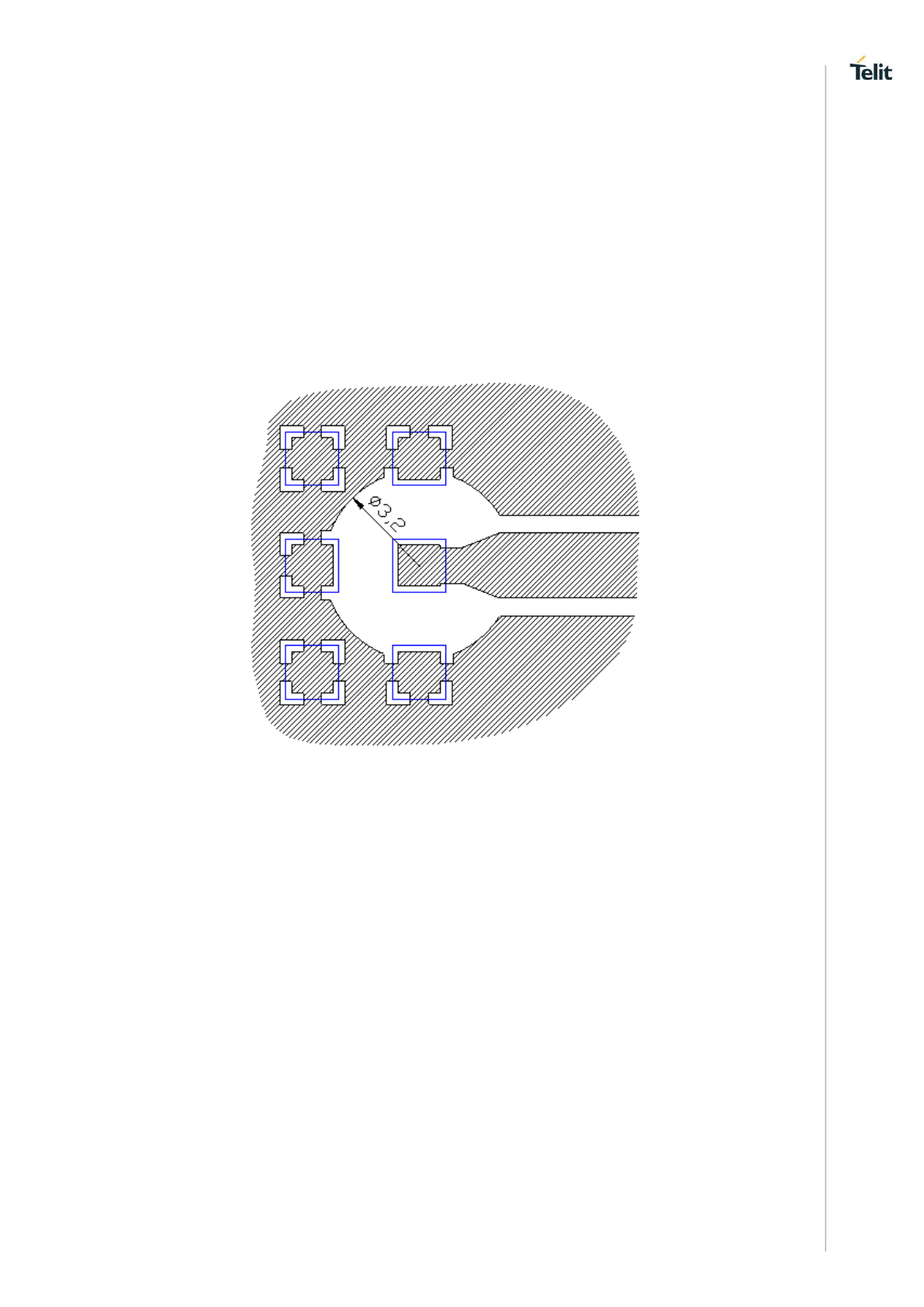
The following image is showing the suggested layout for the Antenna pad connection
(dimensions in mm):
6.1.3. PCB Guidelines in case of FCC Certification
In the case FCC certification is required for an application using LE866, according to FCC
KDB 996369 for modular approval requirements, the transmission line has to be similar to
that implemented on LE866 interface board and described in the following chapter.
6.1.3.1. Transmission line design
During the design of the LE866 interface board, the placement of components has been
chosen properly, in order to keep the line length as short as possible, thus leading to
lowest power losses possible. A Grounded Coplanar Waveguide (G-CPW) line has been
chosen, since this kind of transmission line ensures good impedance control and can be
implemented in an outer PCB layer as needed in this case. A SMA female connector has
been used to feed the line.
LE866 Hardware Design Guide
1VV0301355 Rev. 3 Page 61 of 90 2017-09-07
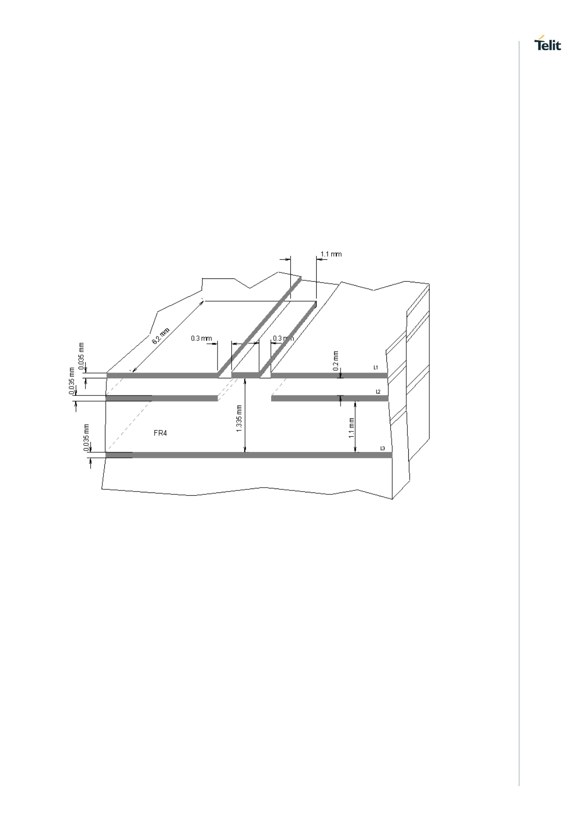
The interface board is realized on a FR4, 4-layers PCB. Substrate material is
characterized by relative permittivity εr = 4.6 ± 0.4 @ 1 GHz, TanD= 0.019 ÷ 0.026 @ 1
GHz.
A characteristic impedance of nearly 50 Ω is achieved using trace width = 1.1 mm,
clearance from coplanar ground plane = 0.3 mm each side. The line uses reference
ground plane on layer 3, while copper is removed from layer 2 underneath the line. Height
of trace above ground plane is 1.335 mm. Calculated characteristic impedance is 51.6 Ω,
estimated line loss is less than 0.1 dB. The line geometry is shown below:
6.1.3.2. Transmission Line Measurements
An HP8753E VNA (Full-2-port calibration) has been used in this measurement session.
A calibrated coaxial cable has been soldered at the pad corresponding to RF output; a
SMA connector has been soldered to the board in order to characterize the losses of the
transmission line including the connector itself. During Return Loss / impedance
measurements, the transmission line has been terminated to 50 Ω load.
LE866 Hardware Design Guide
1VV0301355 Rev. 3 Page 62 of 90 2017-09-07
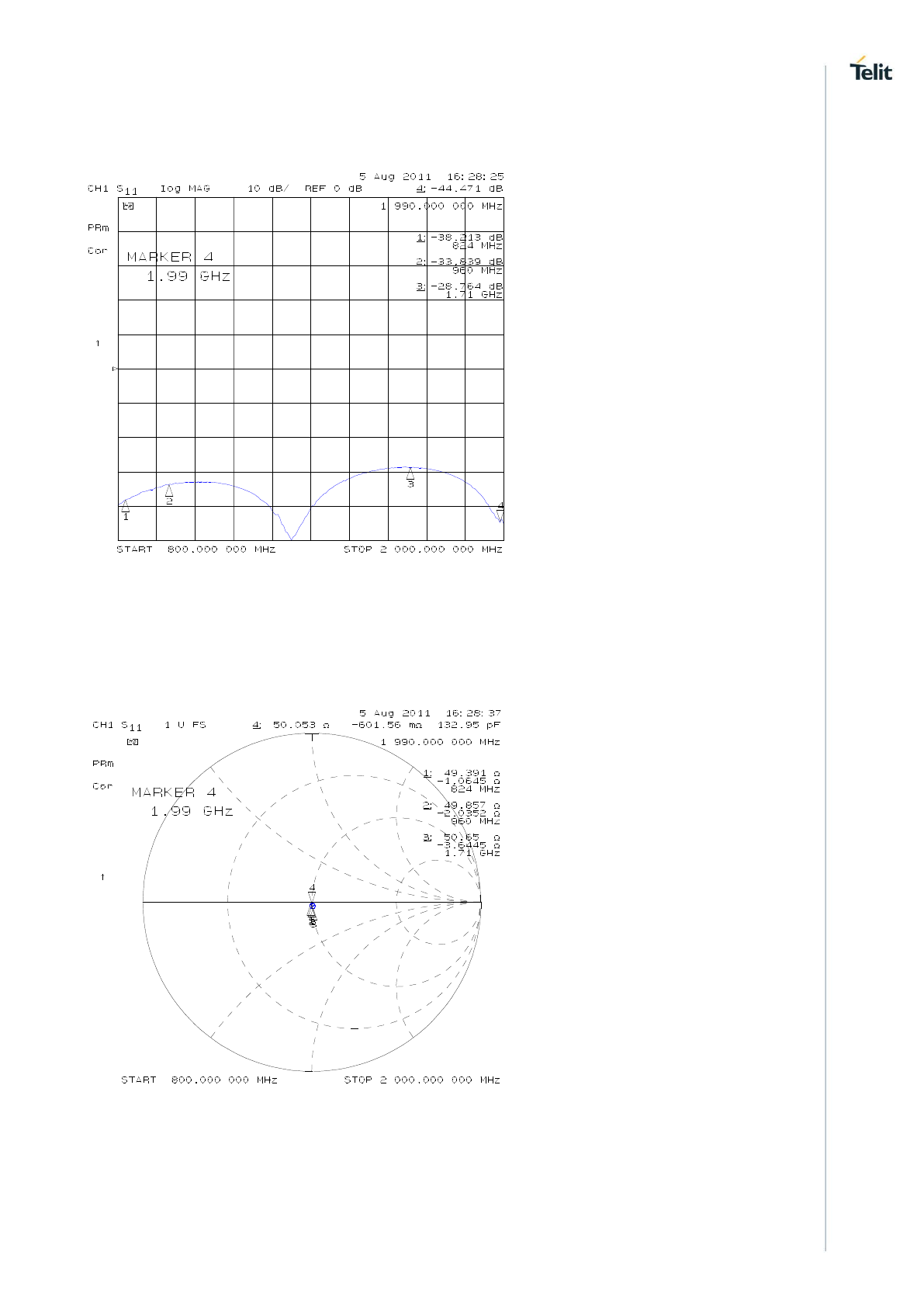
Return Loss plot of line under test is shown below:
Line input impedance (in Smith Chart format, once the line has been terminated to 50 Ω
load) is shown in the following figure:
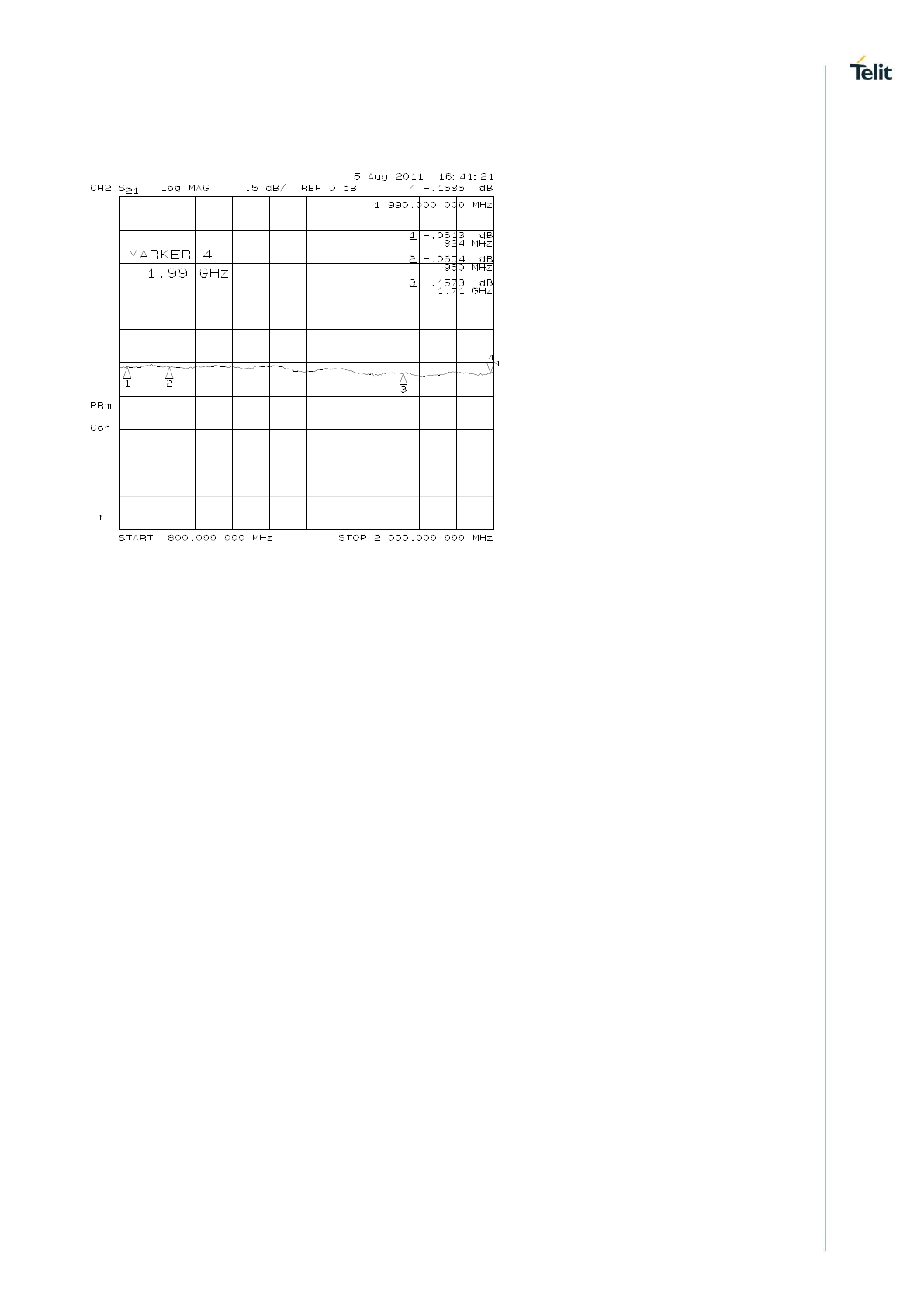
LE866 Hardware Design Guide
1VV0301355 Rev. 3 Page 63 of 90 2017-09-07
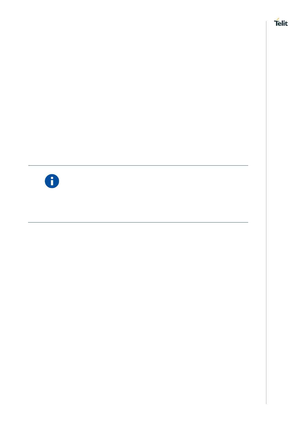
Insertion Loss of G-CPW line plus SMA connector is shown below:
6.1.3.3. Antenna Installation Guidelines
Install the antenna in a place covered by the LTE signal.
If the device antenna is located farther than 20cm from the human body and there are no
co-located transmitter then the Telit FCC/IC approvals can be re-used by the end product.
If the device antenna is located closer than 20cm from the human body or there are co-
located transmitter then the additional FCC/IC testing may be required for the end product
(Telit FCC/IC approvals cannot be reused).
Antenna shall not be installed inside metal cases.
Antenna shall be installed also according to antenna manufacturer instructions.

LE866 Hardware Design Guide
1VV0301355 Rev. 3 Page 64 of 90 2017-09-07
Second Antenna requirements
This product is including an input for a second RX antenna to improve the data
throughput. The function is called Antenna Diversity (downlink MIMO) in LTE.
Item
Value
Frequency range
Depending by frequency band(s) provided by the network
operator, the customer shall use the most suitable antenna
for that/those band(s)
Bandwidth
LTE Band I (2100) : 60 MHz
LTE Band II (1900) : 60 MHz
LTE Band III (1800) : 170 MHz
LTE Band IV (1700) : 45 MHz
LTE Band V (850) : 25 MHz
LTE Band VIII (900) : 80 MHz
LTE Band XII (700) : 17 MHz
LTE Band XIII (700) : 10 MHz
Impedance
50 ohm
VSWR recommended
≤ 2:1 (recommended for the best sensitivity performance)
The second Rx antenna should not be located in the close vicinity of main antenna. In
order to improve Diversity Gain, Isolation and reduce mutual interaction, the two antennas
should be located at the maximum reciprocal distance possible, taking into consideration
the available space into the application. For the same reason, the Rx antenna should also
be cross-polarized with respect to the main antenna.
Isolation between main antenna and Rx antenna must be at least 10 dB in all uplink
frequency bands.
Envelope Correlation Coefficient (ECC) value should be as close as possible to zero, for
best diversity performance. ECC values below 0.5 on all frequency bands are
recommended.
LE866 Hardware Design Guide
1VV0301355 Rev. 3 Page 65 of 90 2017-09-07
6.2.1. Single Antenna Operation
In 4G LTE mode, 3GPP standard does not include single antenna operation because
MIMO is the standard downlink configuration in this cellular system and because of
reduced overall downlink performance when one or more neighbor cells are present.
Nevertheless, LE866 might be used with second antenna removed or not connected if this
degradation in performance is accepted: for some MNOs, for example, a single receive
antenna could be permissible with Cat.1 devices that operates at very low data rates
(integrators should always refer to their network-provider to double check requirements
applicability conditions).
When possible, add a 50ohm (or 47ohm) resistor in order to terminate correctly the
secondary receiver input and/or to provide antenna connection for test/debug purposes.
NOTE:
The Single Antenna configuration has to be activated using the
AT#RXDIV command. Please refer to the AT User Guide for the
detailed command’s syntax.
LE866 Hardware Design Guide
1VV0301355 Rev. 3 Page 66 of 90 2017-09-07
7. AUDIO SECTION
The Telit digital audio interface (DVI) of the LE910-V2 Module is based on the I2S serial
bus interface standard. The audio port can be directly connected to end device using digital
interface, or via one of the several compliant codecs (in case an analog audio is needed).
The following table is listing the modules supporting the Digital Audio:
Model
Audio Supported (Yes/No)
LE866-SV1
YES
LE866A1-KK
NO
LE866A1-KS
NO
LE866A1-NA
NO
LE866A1-JS
NO
Electrical Characteristics
The LE866 Module is provided by one DVI digital voice interface.
The Signals are available on the following Pads and alternate function of the GPIOs:
PAD
Signal
I/O
Function
C5
DVI_WA0
I/O
Digital Voice Interface (Word Alignment / LRCLK)
C6
DVI_RX
I
Digital Voice Interface (RX)
D6
DVI_TX
O
Digital Voice Interface (TX)
D5
DVI_CLK
I/O
Digital Voice Interface (BCLK)
Codec examples
Please refer to the Digital Audio Application note.
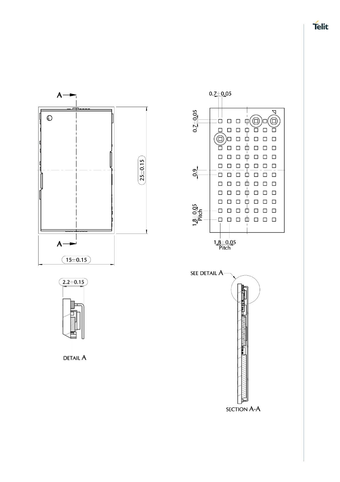
LE866 Hardware Design Guide
1VV0301355 Rev. 3 Page 67 of 90 2017-09-07
8. MECHANICAL DESIGN
Drawing
NOTE: The dimensions are in mm
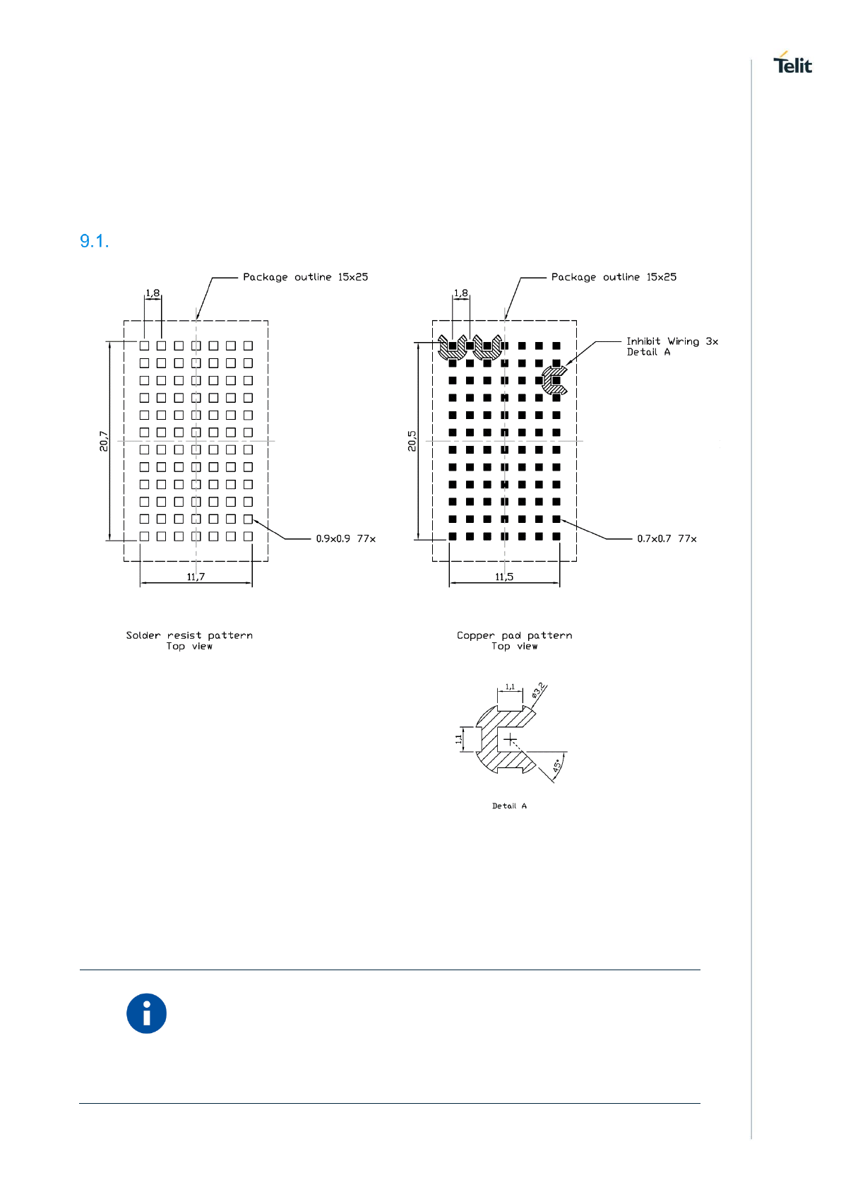
LE866 Hardware Design Guide
1VV0301355 Rev. 3 Page 68 of 90 2017-09-07
9. APPLICATION PCB DESIGN
The LE866 modules have been designed in order to be compliant with a standard lead-
free SMT process.
Footprint
In order to easily rework the LE866 is suggested to consider on the application a 1.5 mm
placement inhibit area around the module. It is also suggested, as common rule for an
SMT component, to avoid having a mechanical part of the application in direct contact
with the module.
NOTE:
In the customer application, the region under WIRING INHIBIT (see
figure above) must be clear from signal or ground paths.
Units: mm
General Tolerance +- 0.05
Angular Tolerance +-1°
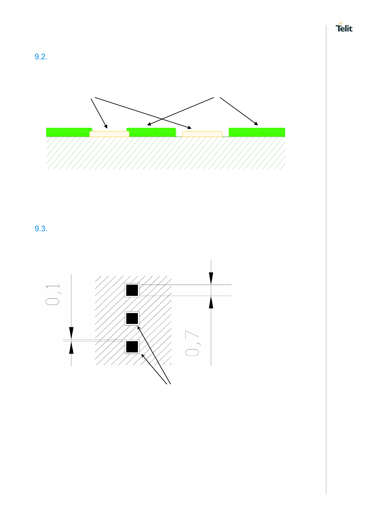
LE866 Hardware Design Guide
1VV0301355 Rev. 3 Page 69 of 90 2017-09-07
PCB pad design
Non solder mask defined (NSMD) type is recommended for the solder pads on the PCB.
PCB pad dimensions
The recommendation for the PCB pads dimensions are described in the following image
(dimensions in mm)
It is not recommended to place via or micro-via not covered by solder resist in an area of
0,3 mm around the pads unless it carries the same signal of the pad itself.
PCB
Copper Pad
Solder Mask
SMD
(Solder Mask Defined)
NSMD
(Non Solder Mask Defined)
Solder resist
openings
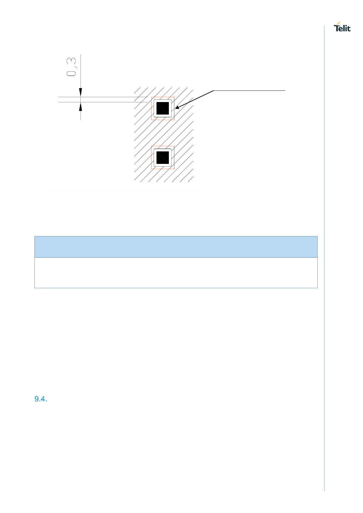
LE866 Hardware Design Guide
1VV0301355 Rev. 3 Page 70 of 90 2017-09-07
Holes in pad are allowed only for blind holes and not for through holes.
Recommendations for PCB pad surfaces:
Finish
Layer Thickness (um)
Properties
Electro-less Ni / Immersion Au
3 –7 / 0.05 – 0.15
good solder ability protection,
high shear force values
The PCB must be able to resist the higher temperatures which are occurring at the lead-
free process. This issue should be discussed with the PCB-supplier. Generally, the
wettability of tin-lead solder paste on the described surface plating is better compared to
lead-free solder paste.
It is not necessary to panel the application’s PCB, however in that case it is suggested to
use milled contours and predrilled board breakouts; scoring or v-cut solutions are not
recommended.
Stencil
Stencil’s apertures layout can be the same of the recommended footprint (1:1), we
suggest a thickness of stencil foil ≥ 120 µm.
Inhibit area for micro-via
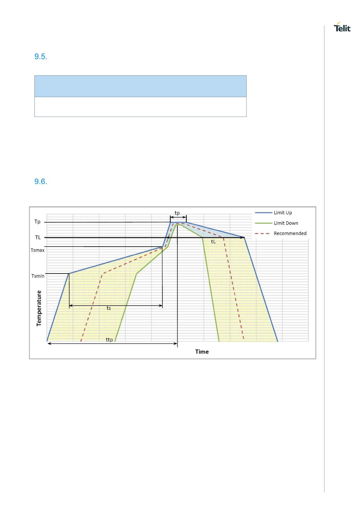
LE866 Hardware Design Guide
1VV0301355 Rev. 3 Page 71 of 90 2017-09-07
Solder paste
Item
Lead Free
Solder Paste
Sn/Ag/Cu
We recommend using only “no clean” solder paste in order to avoid the cleaning of the
modules after assembly.
Solder Reflow
Recommended solder reflow profile:
LE866 Hardware Design Guide
1VV0301355 Rev. 3 Page 72 of 90 2017-09-07
Profile Feature
Pb-Free Assembly
Average ramp-up rate (TL to TP)
3°C/second max
Preheat
– Temperature Min (Tsmin)
– Temperature Max (Tsmax)
– Time (min to max) (ts)
150°C
200°C
60-180 seconds
Tsmax to TL
– Ramp-up Rate
3°C/second max
Time maintained above:
– Temperature (TL)
– Time (tL)
217°C
60-150 seconds
Peak Temperature (Tp)
245 +0/-5°C
Time within 5°C of actual Peak
Temperature (tp)
10-30 seconds
Ramp-down Rate
6°C/second max.
Time 25°C to Peak Temperature
8 minutes max.
NOTE:
All temperatures refer to topside of the package, measured on the
package body surface
WARNING:
THE LE866 MODULE WITHSTANDS ONE REFLOW PROCESS
ONLY.
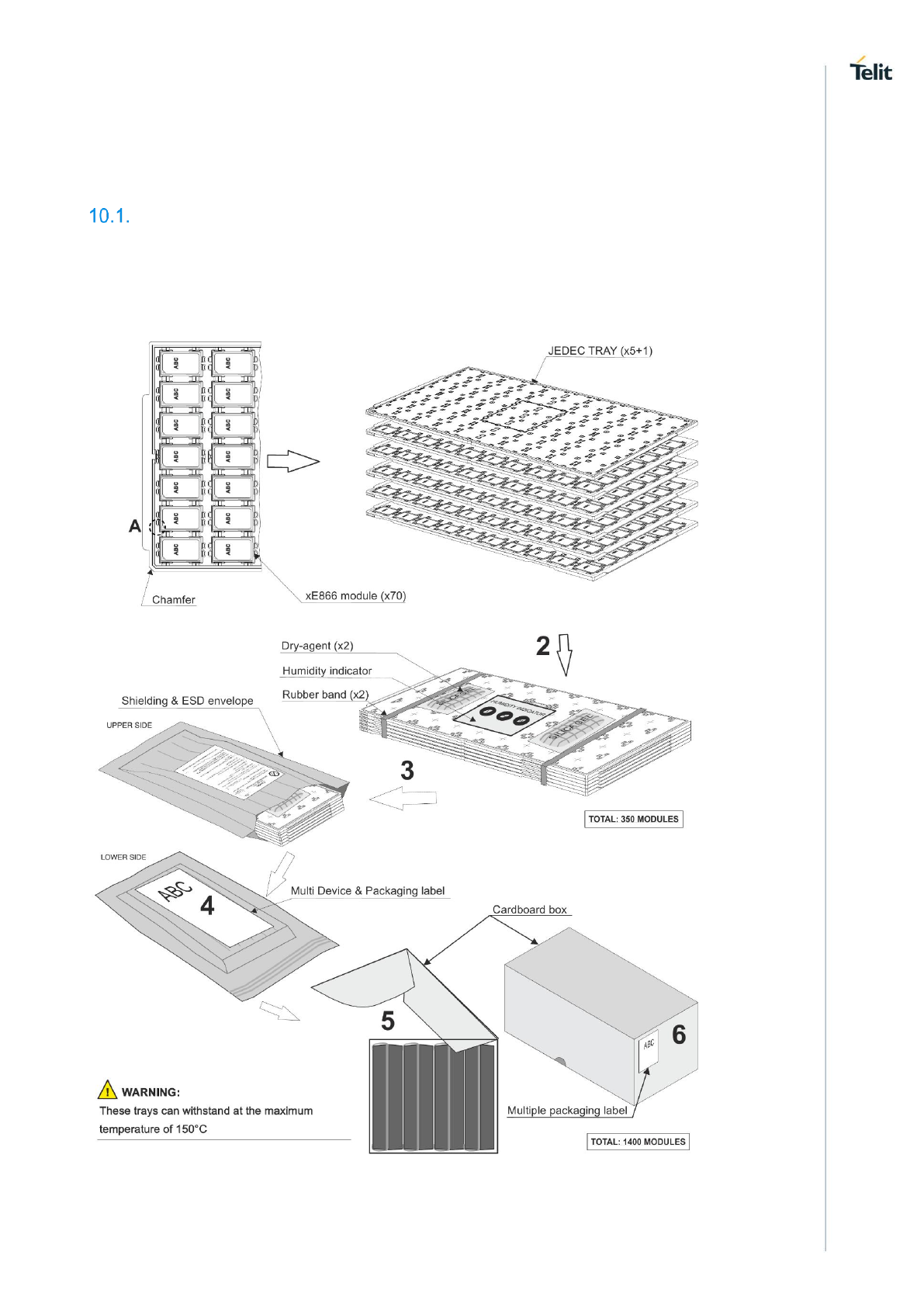
LE866 Hardware Design Guide
1VV0301355 Rev. 3 Page 73 of 90 2017-09-07
10. PACKAGING
Tray
The LE866 modules are packaged on trays of 70 pieces each. These trays can be used in
SMT processes for pick & place handling.
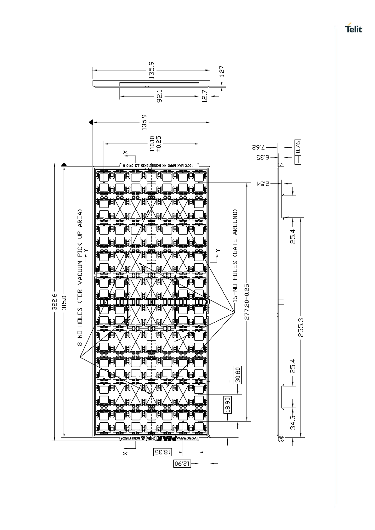
LE866 Hardware Design Guide
1VV0301355 Rev. 3 Page 74 of 90 2017-09-07

LE866 Hardware Design Guide
1VV0301355 Rev. 3 Page 75 of 90 2017-09-07
Moisture sensitivity
The LE866 is a Moisture Sensitive Device level 3, in according with standard IPC/JEDEC
J-STD-020, take care all the relatives requirements for using this kind of components.
Moreover, the customer has to take care of the following conditions:
a) Calculated shelf life in sealed bag: 12 months at <40°C and <90% relative humidity
(RH).
b) Environmental condition during the production: 30°C / 60% RH according to
IPC/JEDEC J-STD-033A paragraph 5.
c) The maximum time between the opening of the sealed bag and the reflow process must
be 168 hours if condition b) “IPC/JEDEC J-STD-033A paragraph 5.2” is respected
d) Baking is required if conditions b) or c) are not respected
e) Baking is required if the humidity indicator inside the bag indicates 10% RH
or more.

LE866 Hardware Design Guide
1VV0301355 Rev. 3 Page 76 of 90 2017-09-07
11. CONFORMITY ASSESSMENT ISSUES
Approvals
GCF (LE866-SV1)
PTCRB (LE866A1-NA)
FCC, IC (LE866A1-NA, LE866-SV1)
KC (LE866A1-KK, LE866A1-KS)
JRL (a.k.a. TELEC) / JTBL (a.k.a. JATE) (LE866A1-JS)
RoHS and REACH (all versions)
Approvals for major Mobile Network Operators
Declaration of Conformity
The DoC is available here: http://www.telit.com/RED/
FCC certificates
The FCC Certificate is available here: https://www.fcc.gov/oet/ea/fccid
IC/ISED certificates
The ISED Certificate is available here:
https://sms-sgs.ic.gc.ca/equipmentSearch/searchRadioEquipments?execution=e1s1&lang=en
FCC/ISED Regulatory notices LE866-SV1
Modification statement
Telit has not approved any changes or modifications to this device by the user. Any changes
or modifications could void the user’s authority to operate the equipment.
Telit n’approuve aucune modification apportée à l’appareil par l’utilisateur, quelle qu’en soit
la nature. Tout changement ou modification peuvent annuler le droit d’utilisation de
l’appareil par l’utilisateur.
Interference statement
This device complies with Part 15 of the FCC Rules and Industry Canada licence-exempt
RSS standard(s). Operation is subject to the following two conditions: (1) this device may
not cause interference, and (2) this device must accept any interference, including
interference that may cause undesired operation of the device.

LE866 Hardware Design Guide
1VV0301355 Rev. 3 Page 77 of 90 2017-09-07
Le présent appareil est conforme aux CNR d’Industrie Canada applicables aux appareils
radio exempts de licence. L’exploitation est autorisée aux deux conditions suivantes : (1)
l’appareil ne doit pas produire de brouillage, et (2) l’utilisateur de l’appareil doit accepter
tout brouillage radioélectrique subi, même si le brouillage est susceptible d’en
compromettre le fonctionnement.
RF exposure
This equipment complies with FCC radiation exposure limits set forth for an uncontrolled
environment. The antenna should be installed and operated with minimum distance of 20
cm between the radiator and your body. Antenna gain must be below:
Product
Band
Antenna Gain (dBi)
LE866-SV1
LTE FDD B4
LTE FDD B13
12.9
6.0
Cet appareil est conforme aux limites d’exposition aux rayonnements de l’ISED pour un
environnement non contrôlé. L’antenne doit être installé de façon à garder une distance
minimale de 20 centimètres entre la source de rayonnements et votre corps. Gain de
l’antenne doit être ci-dessous :
Product
Band
Antenna Gain (dBi)
LE866-SV1
LTE FDD B4
LTE FDD B13
12.9
6.0
This transmitter must not be co-located or operating in conjunction with any other antenna
or transmitter.
L’émetteur ne doit pas être colocalisé ni fonctionner conjointement avec à autre antenne
ou autre émetteur.

LE866 Hardware Design Guide
1VV0301355 Rev. 3 Page 78 of 90 2017-09-07
FCC Class B digital device notice
This equipment has been tested and found to comply with the limits for a Class B digital
device, pursuant to part 15 of the FCC Rules. These limits are designed to provide
reasonable protection against harmful interference in a residential installation. This
equipment generates, uses and can radiate radio frequency energy and, if not installed and
used in accordance with the instructions, may cause harmful interference to radio
communications. However, there is no guarantee that interference will not occur in a
particular installation. If this equipment does cause harmful interference to radio or
television reception, which can be determined by turning the equipment off and on, the user
is encouraged to try to correct the interference by one or more of the following measures:
Reorient or relocate the receiving antenna.
Increase the separation between the equipment and receiver.
Connect the equipment into an outlet on a circuit different from that to which the
receiver is connected.
Consult the dealer or an experienced radio/TV technician for help.
Labelling Requirements for the Host device
The host device shall be properly labelled to identify the modules within the host device.
The certification label of the module shall be clearly visible at all times when installed in the
host device, otherwise the host device must be labelled to display the FCC ID and ISED of
the module, preceded by the words “Contains transmitter module”, or the word “Contains”,
or similar wording expressing the same meaning, as follows:
L’appareil hôte doit être étiqueté comme il faut pour permettre l’identification des modules
qui s’y trouvent. L’étiquette de certification du module donné doit être posée sur l’appareil
hôte à un endroit bien en vue en tout temps. En l’absence d’étiquette, l’appareil hôte doit
porter une étiquette donnant le FCC ID et l’ISED du module, précédé des mots « Contient
un module d’émission », du mot « Contient » ou d’une formulation similaire exprimant le
même sens, comme suit :
LE866-SV1
Contains FCC ID : RI7LE866SV1
Contains IC : 5131A-LE866SV1

LE866 Hardware Design Guide
1VV0301355 Rev. 3 Page 79 of 90 2017-09-07
CAN ICES-3 (B) / NMB-3 (B)
This Class B digital apparatus complies with Canadian ICES-003.
Cet appareil numérique de classe B est conforme à la norme canadienne ICES-003.

LE866 Hardware Design Guide
1VV0301355 Rev. 3 Page 80 of 90 2017-09-07
FCC/ISED Regulatory notices LE866A1-NA
Modification statement
Telit has not approved any changes or modifications to this device by the user. Any changes
or modifications could void the user’s authority to operate the equipment.
Telit n’approuve aucune modification apportée à l’appareil par l’utilisateur, quelle qu’en soit
la nature. Tout changement ou modification peuvent annuler le droit d’utilisation de
l’appareil par l’utilisateur.
Interference statement
This device complies with Part 15 of the FCC Rules and Industry Canada licence-exempt
RSS standard(s). Operation is subject to the following two conditions: (1) this device may
not cause interference, and (2) this device must accept any interference, including
interference that may cause undesired operation of the device.
Le présent appareil est conforme aux CNR d’Industrie Canada applicables aux appareils
radio exempts de licence. L’exploitation est autorisée aux deux conditions suivantes : (1)
l’appareil ne doit pas produire de brouillage, et (2) l’utilisateur de l’appareil doit accepter
tout brouillage radioélectrique subi, même si le brouillage est susceptible d’en
compromettre le fonctionnement.
RF exposure
This equipment complies with FCC radiation exposure limits set forth for an uncontrolled
environment. The antenna should be installed and operated with minimum distance of 20
cm between the radiator and your body. For FCC the Max antenna gain must be as in below
table:
Product
Band
Antenna
Gain
LE866A1-NA
Max Gain in Lower operational Band f < 1GHz (LTE Band 12)
Max Gain in Higher operational Band (1700 MHz) (LTE Band 4)
Max Gain in Higher operational Band (1900 MHz) (LTE Band 2)
9.70 dBi
6.00 dBi
9.01 dBi

LE866 Hardware Design Guide
1VV0301355 Rev. 3 Page 81 of 90 2017-09-07
Cet appareil est conforme aux limites d’exposition aux rayonnements de l’ISED pour un
environnement non contrôlé. L’antenne doit être installé de façon à garder une distance
minimale de 20 centimètres entre la source de rayonnements et votre corps. Gain de
l’antenne doit être ci-dessous :
Product
Band
Antenna
Gain
LE866A1-NA
Max Gain in Lower operational Band f < 1GHz (LTE Band 12)
Max Gain in Higher operational Band (1700 MHz) (LTE Band 4)
Max Gain in Higher operational Band (1900 MHz) (LTE Band 2)
6.61 dBi
6.00 dBi
9.01 dBi
If the device has to be compliant to FCC and ISED the limits are the following:
Product
Band
Antenna
Gain
LE866A1-NA
Max Gain in Lower operational Band f < 1GHz (LTE Band 12)
Max Gain in Higher operational Band (1700 MHz) (LTE Band 4)
Max Gain in Higher operational Band (1900 MHz) (LTE Band 2)
6.61 dBi
6.00 dBi
9.01 dBi
This transmitter must not be co-located or operating in conjunction with any other antenna
or transmitter.
L’émetteur ne doit pas être colocalisé ni fonctionner conjointement avec à autre antenne
ou autre émetteur.
FCC Class B digital device notice
This equipment has been tested and found to comply with the limits for a Class B digital
device, pursuant to part 15 of the FCC Rules. These limits are designed to provide
reasonable protection against harmful interference in a residential installation. This
equipment generates, uses and can radiate radio frequency energy and, if not installed and
used in accordance with the instructions, may cause harmful interference to radio
communications. However, there is no guarantee that interference will not occur in a
particular installation. If this equipment does cause harmful interference to radio or

LE866 Hardware Design Guide
1VV0301355 Rev. 3 Page 82 of 90 2017-09-07
television reception, which can be determined by turning the equipment off and on, the user
is encouraged to try to correct the interference by one or more of the following measures:
Reorient or relocate the receiving antenna.
Increase the separation between the equipment and receiver.
Connect the equipment into an outlet on a circuit different from that to which the
receiver is connected.
Consult the dealer or an experienced radio/TV technician for help.
Labelling Requirements for the Host device
The host device shall be properly labelled to identify the modules within the host device.
The certification label of the module shall be clearly visible at all times when installed in the
host device, otherwise the host device must be labelled to display the FCC ID and ISED of
the module, preceded by the words “Contains transmitter module”, or the word “Contains”,
or similar wording expressing the same meaning, as follows:
L’appareil hôte doit être étiqueté comme il faut pour permettre l’identification des modules
qui s’y trouvent. L’étiquette de certification du module donné doit être posée sur l’appareil
hôte à un endroit bien en vue en tout temps. En l’absence d’étiquette, l’appareil hôte doit
porter une étiquette donnant le FCC ID et l’ISED du module, précédé des mots « Contient
un module d’émission », du mot « Contient » ou d’une formulation similaire exprimant le
même sens, comme suit :
LE866A1-NA
Contains FCC ID : RI7XE866A1NA
Contains IC : 5131A-XE866A1NA
CAN ICES-3 (B) / NMB-3 (B)
This Class B digital apparatus complies with Canadian ICES-003.
Cet appareil numérique de classe B est conforme à la norme canadienne ICES-003.

LE866 Hardware Design Guide
1VV0301355 Rev. 3 Page 83 of 90 2017-09-07
12. SAFETY RECOMMENDATIONS
READ CAREFULLY
Be sure the use of this product is allowed in the country and in the environment required.
The use of this product may be dangerous and has to be avoided in the following areas:
Where it can interfere with other electronic devices in environments such as
hospitals, airports, aircrafts, etc.
Where there is risk of explosion such as gasoline stations, oil refineries, etc. It is the
responsibility of the user to enforce the country regulation and the specific
environment regulation.
Do not disassemble the product; any mark of tampering will compromise the warranty
validity. We recommend following the instructions of the hardware user guides for correct
wiring of the product. The product has to be supplied with a stabilized voltage source and
the wiring has to be conformed to the security and fire prevention regulations. The product
has to be handled with care, avoiding any contact with the pins because electrostatic
discharges may damage the product itself. Same cautions have to be taken for the SIM,
checking carefully the instruction for its use. Do not insert or remove the SIM when the
product is in power saving mode.
The system integrator is responsible for the functioning of the final product; therefore, care
has to be taken to the external components of the module, as well as any project or
installation issue, because the risk of disturbing the LTE network or external devices or
having impact on the security. Should there be any doubt, please refer to the technical
documentation and the regulations in force. Every module has to be equipped with a proper
antenna with specific characteristics. The antenna has to be installed with care in order to
avoid any interference with other electronic devices and has to guarantee a minimum
distance from the body (20 cm). In case this requirement cannot be satisfied, the system
integrator has to assess the final product against the SAR regulation.
The European Community provides some Directives for the electronic equipment
introduced on the market. All of the relevant information is available on the European
Community website:
http://ec.europa.eu/enterprise/sectors/rtte/documents/
The text of the Directive 99/05 regarding telecommunication equipment is available,
while the applicable Directives (Low Voltage and EMC) are available at:
http://ec.europa.eu/enterprise/sectors/electrical/
LE866 Hardware Design Guide
1VV0301355 Rev. 3 Page 84 of 90 2017-09-07
13. REFERENCE TABLE OF RF BANDS CHARACTERISTICS
Mode
Freq. Tx
(MHz)
Freq. Rx
(MHz)
Channels
Tx-Rx Offset
PCS 1900
1850.2 ~ 1909.8
1930.2 ~ 1989.8
512 ~ 810
80 MHz
DCS 1800
1710 ~ 1785
1805 ~ 1880
512 ~ 885
95 MHz
GSM 850
824.2 ~ 848.8
869.2 ~ 893.8
128 ~ 251
45 MHz
EGSM 900
890 ~ 915
935 ~ 960
0 ~ 124
45 MHz
880 ~ 890
925 ~ 935
975 ~ 1023
45 MHz
WCDMA 2100 – B1
1920 ~ 1980
2110 ~ 2170
Tx: 9612 ~ 9888
Rx: 10562 ~ 10838
190 MHz
WCDMA 1900 – B2
1850 ~ 1910
1930 ~ 1990
Tx: 9262 ~ 9538
Rx: 9662 ~ 9938
80 MHz
WCDMA 1800 – B3
1710 ~ 1785
1805 ~ 1880
Tx: 937 ~ 1288
Rx: 1162 ~ 1513
95 MHz
WCDMA AWS – B4
1710 ~ 1755
2110 ~ 2155
Tx: 1312 ~ 1513
Rx: 1537 ~ 1738
400 MHz
WCDMA 850 – B5
824 ~ 849
869 ~ 894
Tx: 4132 ~ 4233
Rx: 4357 ~ 4458
45 MHz
WCDMA 900 – B8
880 ~ 915
925 ~ 960
Tx: 2712 ~ 2863
Rx: 2937 ~ 3088
45 MHz
WCDMA 1800 – B9
1750 ~ 1784.8
1845 ~ 1879.8
Tx: 8762 ~ 8912
Rx: 9237 ~ 9387
95 MHz
WCDMA 800 – B19
830 ~ 845
875 ~ 890
Tx: 312 ~ 363
Rx: 712 ~ 763
45 MHz
TDSCDMA 2000 – B34
2010 ~ 2025
2010 ~ 2025
Tx: 10054 ~ 10121
Rx: 10054 ~ 10121
0 MHz
TDSCDMA 1900 – B39
1880 ~ 1920
1880 ~ 1920
Tx: 9404 ~ 9596
Rx: 9404 ~ 9596
0 MHz
LTE 2100 – B1
1920 ~ 1980
2110 ~ 2170
Tx: 18000 ~ 18599
Rx: 0 ~ 599
190 MHz
LE866 Hardware Design Guide
1VV0301355 Rev. 3 Page 85 of 90 2017-09-07
Mode
Freq. Tx
(MHz)
Freq. Rx
(MHz)
Channels
Tx-Rx Offset
LTE 1900 – B2
1850 ~ 1910
1930 ~ 1990
Tx: 18600 ~ 19199
Rx: 600 ~ 1199
80 MHz
LTE 1800 – B3
1710 ~ 1785
1805 ~ 1880
Tx: 19200 ~ 19949
Rx: 1200 ~ 1949
95 MHz
LTE AWS – B4
1710 ~ 1755
2110 ~ 2155
Tx: 19950 ~ 20399
Rx: 1950 ~ 2399
400 MHz
LTE 850 – B5
824 ~ 849
869 ~ 894
Tx: 20400 ~ 20649
Rx: 2400 ~ 2649
45 MHz
LTE 2600 – B7
2500 ~ 2570
2620 ~ 2690
Tx: 20750 ~ 21449
Rx: 2750 ~ 3449
120 MHz
LTE 900 – B8
880 ~ 915
925 ~ 960
Tx: 21450 ~ 21799
Rx: 3450 ~ 3799
45 MHz
LTE 1800 – B9
1749.9 ~ 1784.9
1844.9 ~ 1879.9
Tx: 21800 ~ 2149
Rx: 3800 ~ 4149
95 MHz
LTE AWS+ – B10
1710 ~ 1770
2110 ~ 2170
Tx: 22150 ~ 22749
Rx: 4150 ~ 4749
400 MHz
LTE 700a – B12
699 ~ 716
729 ~ 746
Tx : 23010 ~ 23179
Rx : 5010 ~ 5179
30 MHz
LTE 700c – B13
777 ~ 787
746 ~ 756
Tx : 27210 ~ 27659
Rx : 9210 ~ 9659
-31 MHz
LTE 700b – B17
704 ~ 716
734 ~ 746
Tx: 23730 ~ 23849
Rx: 5730 ~ 5849
30 MHz
LTE 800 – B19
830 ~ 845
875 ~ 890
Tx: 24000 ~ 24149
Rx: 6000 ~ 6149
45 MHz
LTE 800 – B20
832 ~ 862
791 ~ 821
Tx: 24150 ~ 24449
Rx: 6150 ~ 6449
-41 MHz
LTE 1500 – B21
1447.9 ~ 1462.9
1495.9 ~ 1510.9
Tx: 24450 ~ 24599
Rx: 6450 ~ 6599
48 MHz
LTE 850+ – B26
814 ~ 849
859 ~ 894
Tx: 26690 ~ 27039
Rx: 8690 ~ 9039
45 MHz
LE866 Hardware Design Guide
1VV0301355 Rev. 3 Page 86 of 90 2017-09-07
Mode
Freq. Tx
(MHz)
Freq. Rx
(MHz)
Channels
Tx-Rx Offset
LTE 700 – B28
703 ~ 748
758 ~ 803
Tx : 27210 ~ 27659
Rx : 9210 ~ 9659
45 MHz
LTE TDD 2600 – B38
2570 ~ 2620
2570 ~ 2620
Tx: 37750 ~ 38250
Rx: 37750 ~ 38250
0 MHz
LTE TDD 1900 – B39
1880 ~ 1920
1880 ~ 1920
Tx: 38250 ~ 38650
Rx: 38250 ~ 38650
0 MHz
LTE TDD 2300 – B40
2300 ~ 2400
2300 ~ 2400
Tx: 38650 ~ 39650
Rx: 38650 ~ 39650
0 MHz
LTE TDD 2500 – B41
2496 ~ 2690
2496 ~ 2690
Tx: 39650 ~ 41590
Rx: 39650 ~ 41590
0 MHz

LE866 Hardware Design Guide
1VV0301355 Rev. 3 Page 87 of 90 2017-09-07
14. ACRONYMS
TTSC
Telit Technical Support Centre
USB
Universal Serial Bus
HS
High Speed
DTE
Data Terminal Equipment
UMTS
Universal Mobile Telecommunication System
WCDMA
Wideband Code Division Multiple Access
HSDPA
High Speed Downlink Packet Access
HSUPA
High Speed Uplink Packet Access
UART
Universal Asynchronous Receiver Transmitter
HSIC
High Speed Inter Chip
SIM
Subscriber Identification Module
SPI
Serial Peripheral Interface
ADC
Analog – Digital Converter
DAC
Digital – Analog Converter
I/O
Input Output
GPIO
General Purpose Input Output
CMOS
Complementary Metal – Oxide Semiconductor
MOSI
Master Output – Slave Input

LE866 Hardware Design Guide
1VV0301355 Rev. 3 Page 88 of 90 2017-09-07
MISO
Master Input – Slave Output
CLK
Clock
MRDY
Master Ready
SRDY
Slave Ready
CS
Chip Select
RTC
Real Time Clock
PCB
Printed Circuit Board
ESR
Equivalent Series Resistance
VSWR
Voltage Standing Wave Radio
VNA
Vector Network Analyzer

LE866 Hardware Design Guide
1VV0301355 Rev. 3 Page 89 of 90 2017-09-07
15. DOCUMENT HISTORY
Revision
Date
Changes
0
2017-02-06
First issue
This document replaces the LE866 HW User Guide
Doc# 1VV0301210.
1
2017-07-05
Added LE866A1-NA FCC Conformity chapter
2
2017-09-06
Updated LE866A1-NA FCC Conformity chapter
3
2017-09-06
Updated LE866A1-NA FCC Conformity chapter

[01.2017]
Mod.0818 2017-01 Rev.0