Telit Wireless Solutions C11G2 BT Module User Manual BlueRS C11 G2 HWreference V1 0
Stollmann E+V GmbH BT Module BlueRS C11 G2 HWreference V1 0
UserManual.wiki
>
Telit Wireless Solutions
>
C11G2 User Manual
User Manual
Navigation menu
Upload a User Manual
Namespaces
Wiki Guide
HTML
PDF
Info
Views
User Manual
Discussion / Help
Navigation
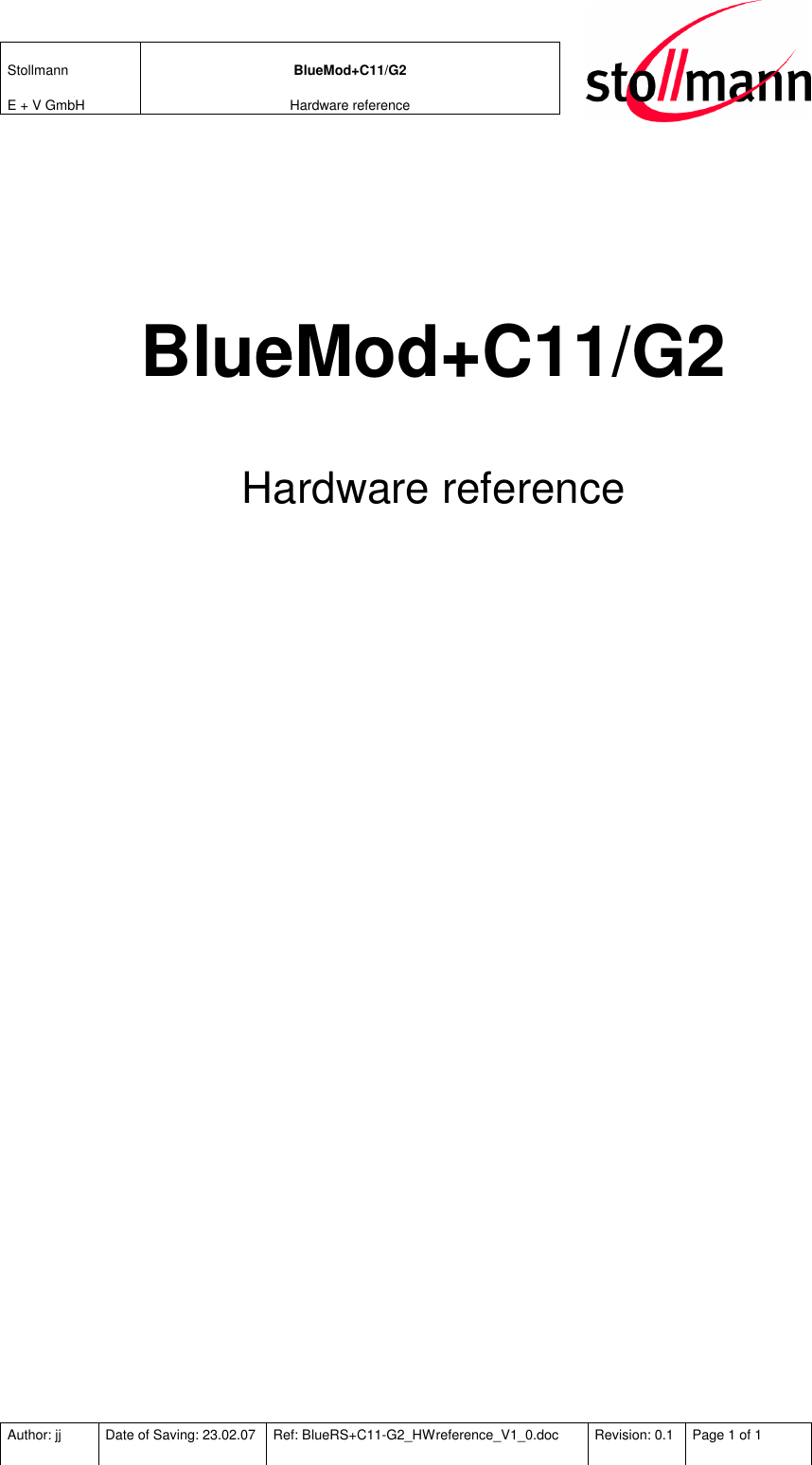
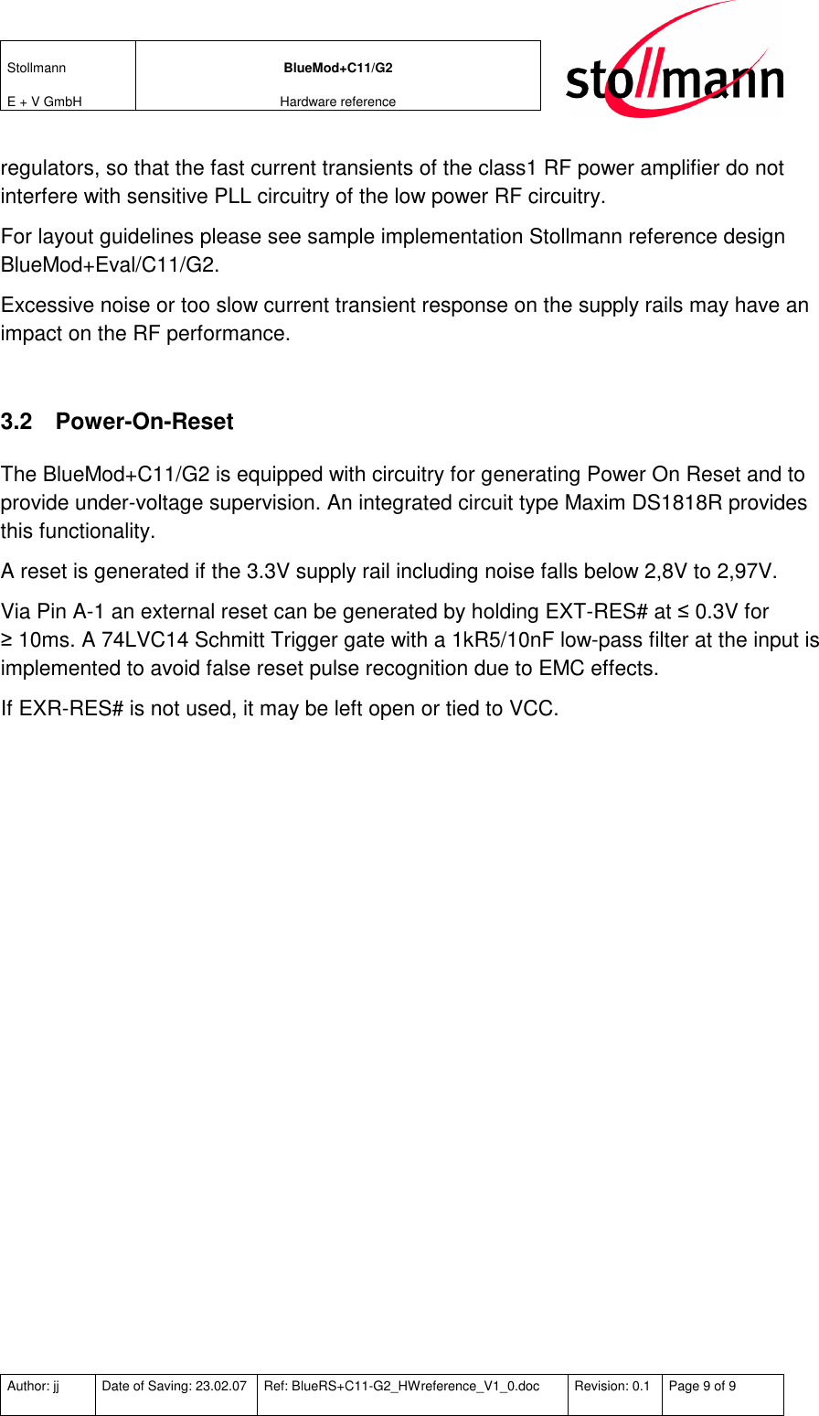
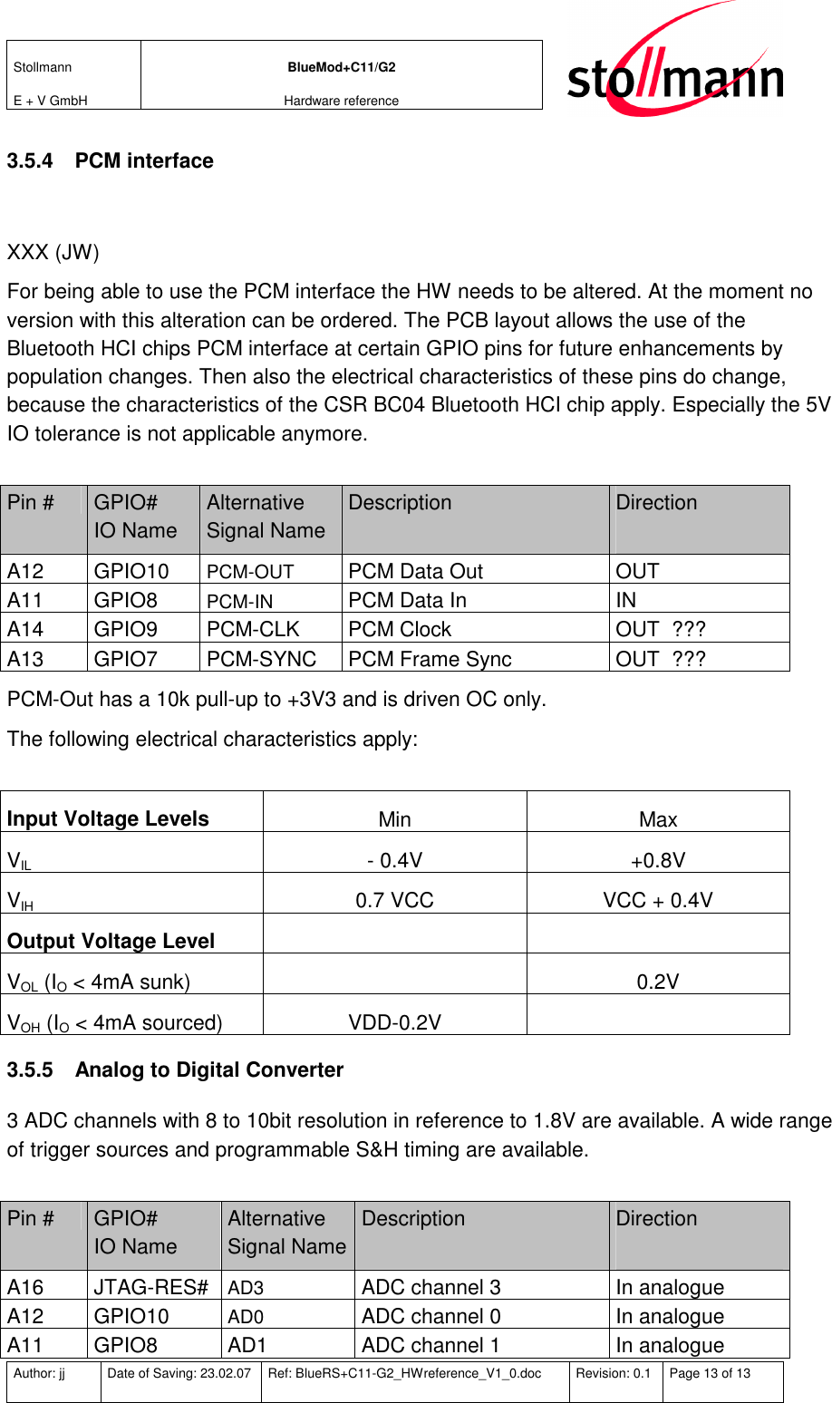
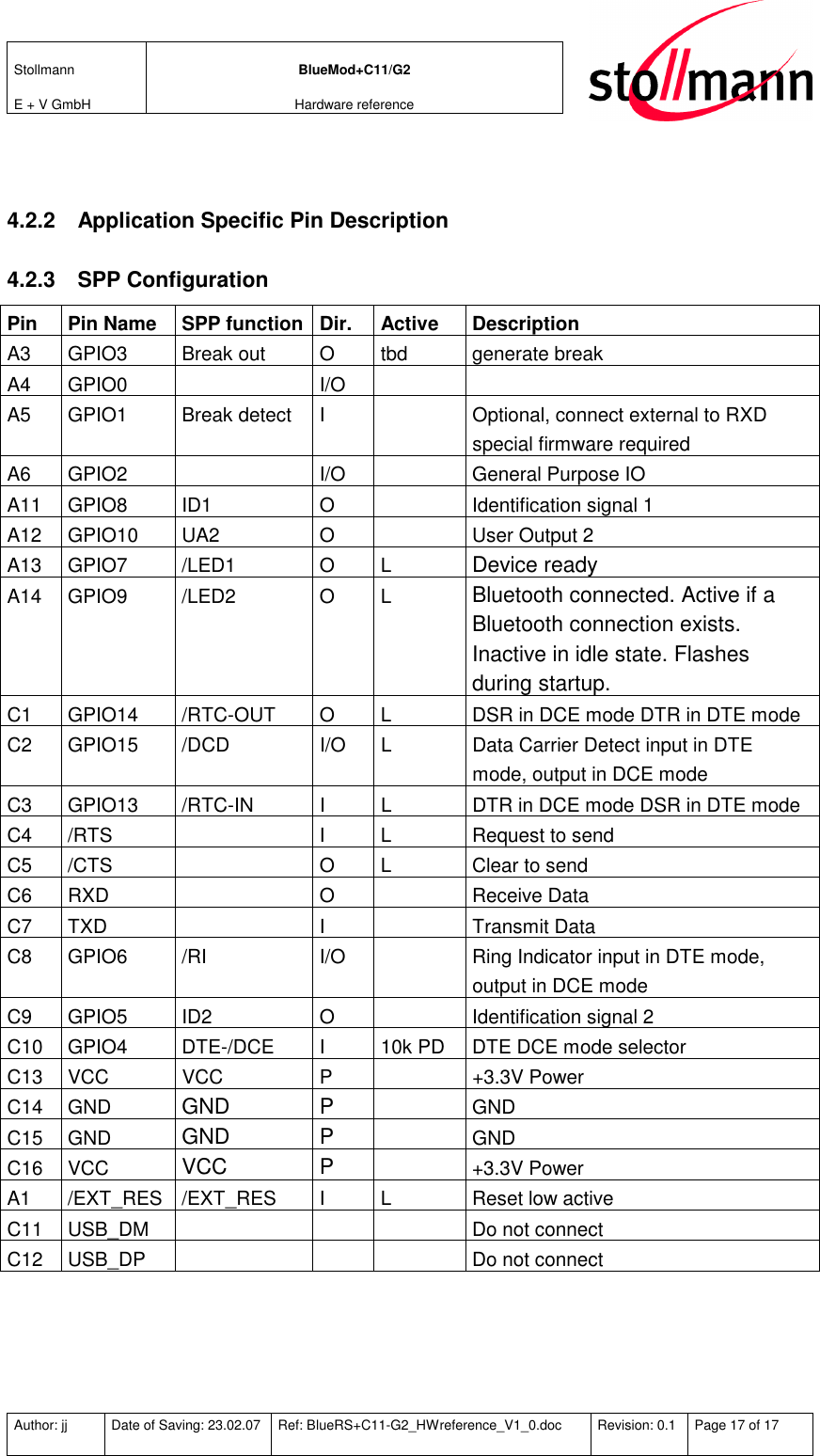
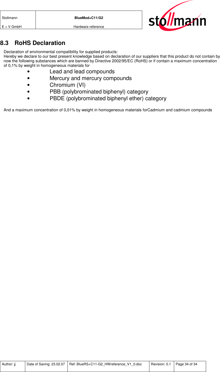
![Stollmann E + V GmbH BlueMod+C11/G2 Hardware reference Author: jj Date of Saving: 23.02.07 Ref: BlueRS+C11-G2_HWreference_V1_0.doc Revision: 0.1 Page 22 of 22 5.4 RF performance Vcc = 3.0V to 3.6V, Tamb = - 40°C to +85°C Receiver Frequency [GHz] Limit BT Unit Min Typ Max Spec 2.402 -90,0 -80,0 2.441 -90,0 -80,0 Sensitivity at 0.1% BER DH1 2.480 -90,0 -80,0 ≤-70 dBm 2.402 -90,0 -80,0 2.441 -90,0 -80,0 Sensitivity at 0.1% BER DH5 2.480 -90,0 -80,0 ≤-70 dBm 2.402 -88,0 -80,0 2.441 -88,0 -80,0 Sensitivity at 0.1% BER PI/4 DQPSK 2.480 -88,0 -80,0 ≤-70 dBm 2.402 -82,0 -74,0 2.441 -82,0 -74,0 Sensitivity at 0.1% BER 8DPSK 2.480 -82,0 -74,0 ≤-70 dBm Maximum received signal at 0.1% BER with DH1 -20,0 >10 ≥-20 dBm Maximum received signal at 0.1% BER with DH5 -20,0 >10 ≥-20 dBm Maximum received signal at 0.1% BER with PI/4 DQPSK -20,0 -12,0 ≥-20 dBm Maximum received signal at 0.1% BER with 8DPSK -20,0 -18,0 ≥-20 dBm](https://usermanual.wiki/Telit-Wireless-Solutions/C11G2/User-Guide-763182-Page-22.png)
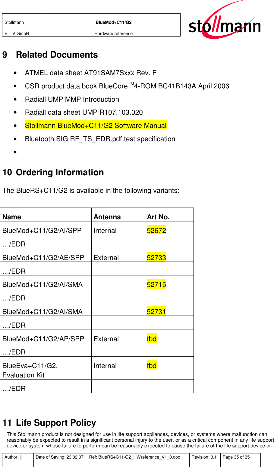
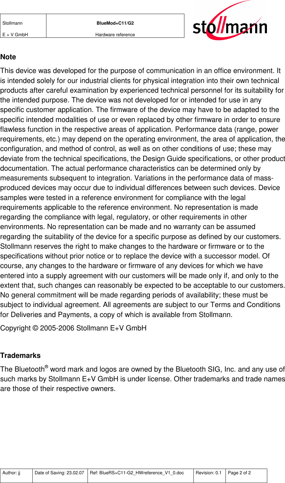
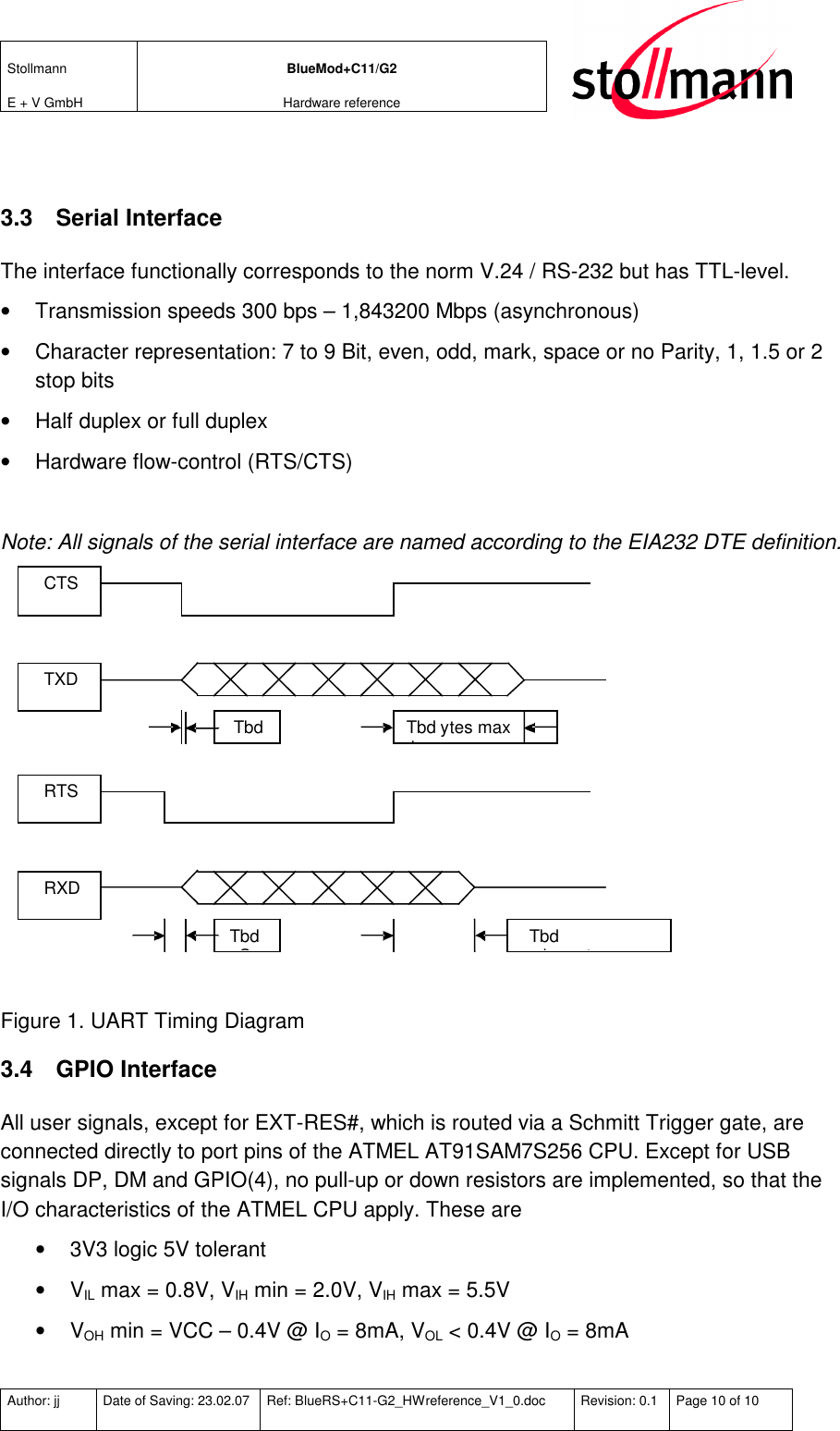
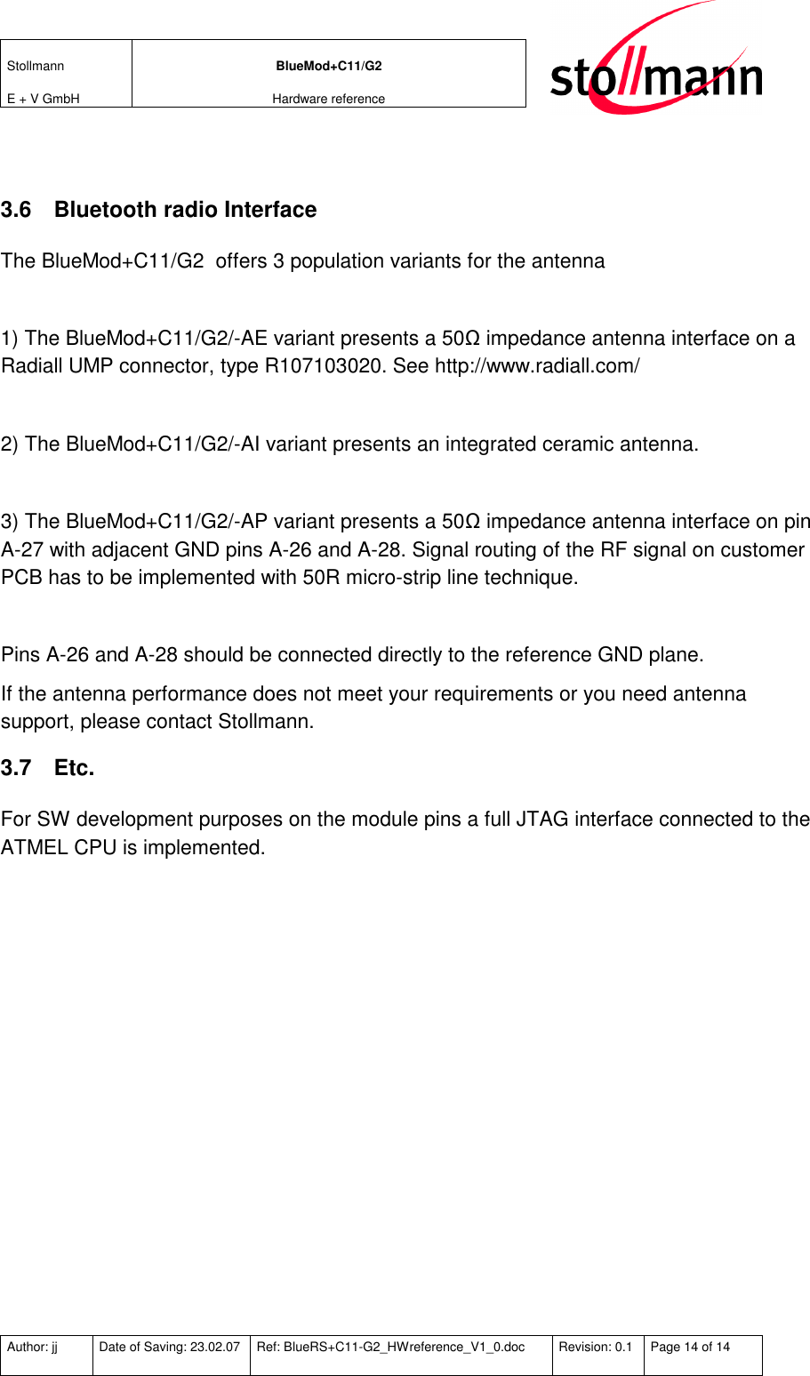
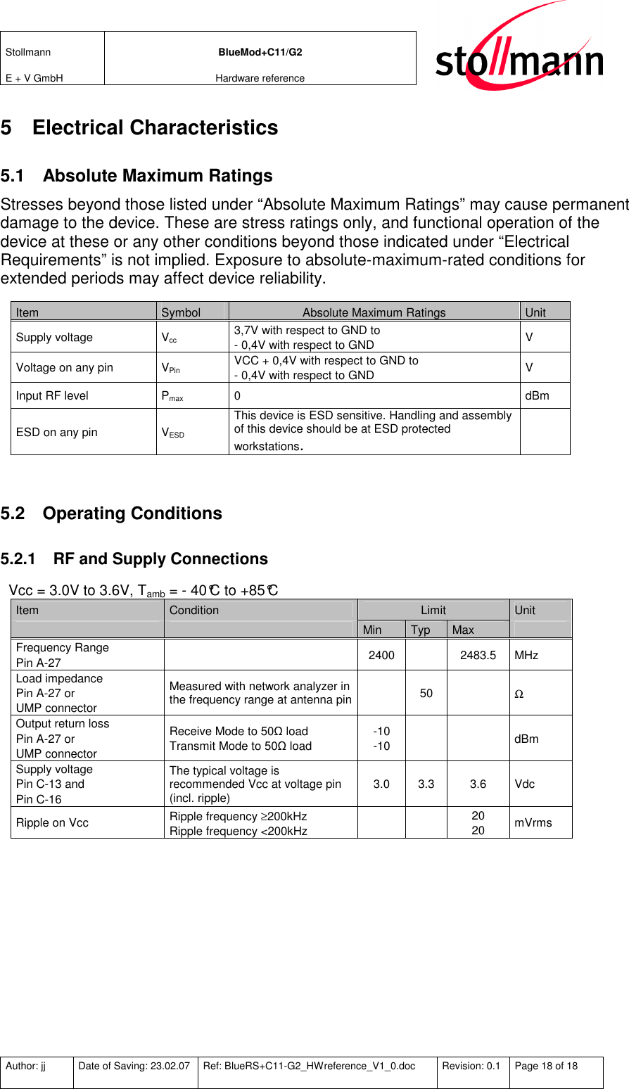
![Stollmann E + V GmbH BlueMod+C11/G2 Hardware reference Author: jj Date of Saving: 23.02.07 Ref: BlueRS+C11-G2_HWreference_V1_0.doc Revision: 0.1 Page 23 of 23 Vcc = 3.0V to 3.6V, Tamb = - 40°C to +85°C Transmitter Frequency [GHz] Limit BT Unit Min Typ Max Spec 2.402 16,0 18,5 19,0 2.441 16,0 18,5 19,0 RF transmit power 50 Ω load, at antenna Class 1 device GFSK a) 2.480 16,0 18,5 19,0 +4 to +20 dBm 2.402 tbd 2.441 tbd RF transmit power 50 Ω load, at antenna Class 1 device EDR2 a) 2.480 tbd 2.402 tbd 2.441 tbd RF transmit power 50 Ω load, at antenna Class 1 device EDR3 a) 2.480 tbd RF power control range 17 dB RF power range control resolution 4 2 to 8 dB 20 dB bandwidth for modulated carrier 780 1000 ≤1000 kHz Initial carrier frequency tolerance 5 30 ≤ ±75 kHz Carrier frequency drift (packet DH1) 7 25 ≤ ±25 kHz Drift Rate 6 20 20 kHz/ 50µs ∆f1avg “Maximum Modulation” 140 165 175 ≥140 to ≤175 kHz ∆f2avg “Minimum Modulation” 115 154 ≥ 115 kHz C/I co-channel b) 8 11 ≤ 11 dB Adjacent channel selectivity C/I f = f0 + 1MHz b) -6 0 ≤ 0 dB Adjacent channel selectivity C/I f = f0 - 1MHz b) -4 0 ≤ 0 dB Adjacent channel selectivity C/I f ≥ f0 + 2MHz b) -38 -30 ≤ -30 dB Adjacent channel selectivity C/I f ≤ f0 - 2MHz b) -24 -20 ≤ -30 dB Adjacent channel selectivity C/I f ≥ f0 + 3MHz b) -45 -40 ≤ -40 dB Adjacent channel selectivity C/I f ≤ f0 - 5MHz b) -45 -40 ≤ -40 dB Adjacent channel selectivity C/I f = fimage b) -21 -9 ≤ -9 dB Notes: a) Including +2dBi antenna gain b) Applies according to BT Test Specification Ver. 1.2/2.0/2.0 + EDR only for Tamb = 20°C](https://usermanual.wiki/Telit-Wireless-Solutions/C11G2/User-Guide-763182-Page-23.png)
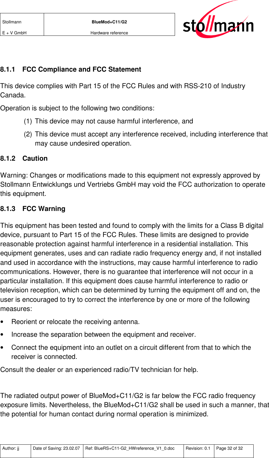
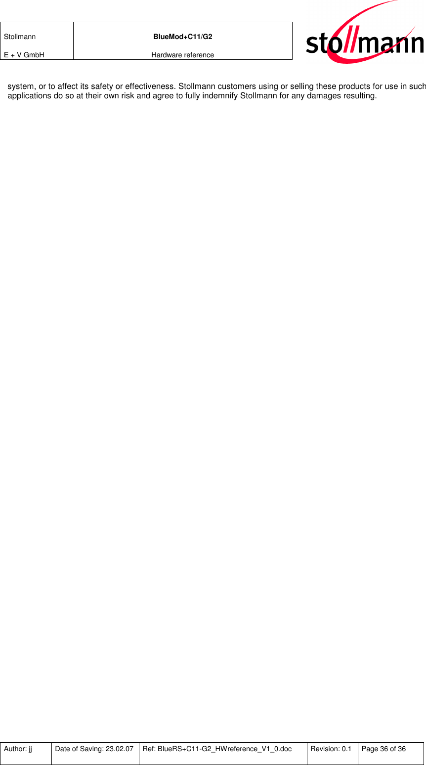
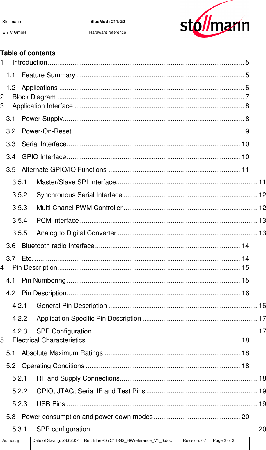
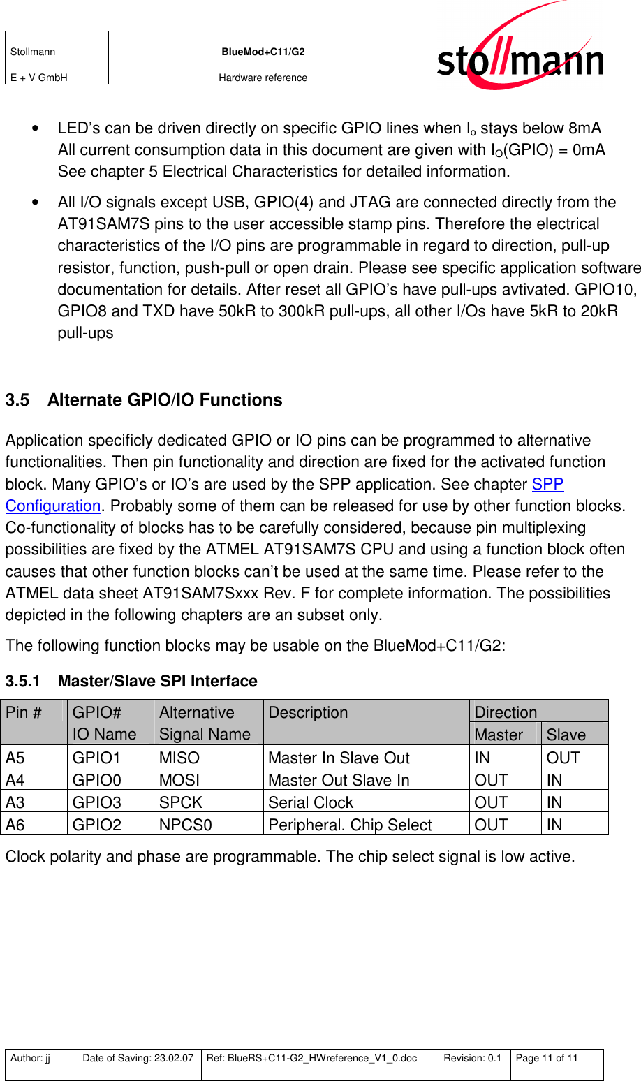
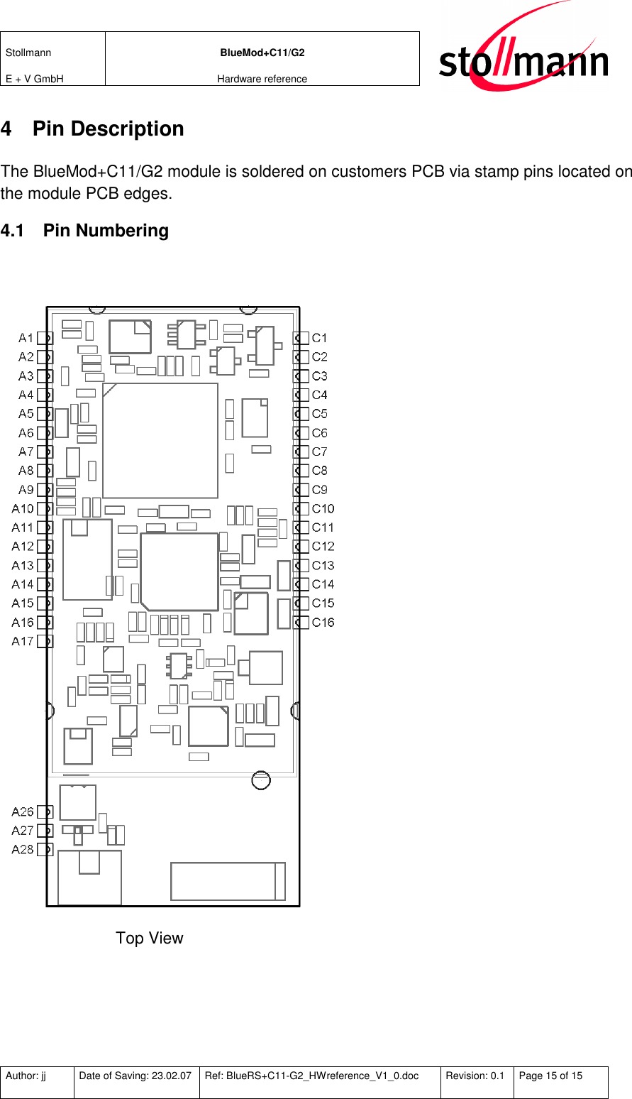
![Stollmann E + V GmbH BlueMod+C11/G2 Hardware reference Author: jj Date of Saving: 23.02.07 Ref: BlueRS+C11-G2_HWreference_V1_0.doc Revision: 0.1 Page 25 of 25 6 Mechanical Characteristics 6.1 Dimensions 6.2 Connectors Except for the stamp pins A-[1-17,26-28] and C-[1-16] and the UMP antenna connector no user accessible connectors are implemented. If the use of the UMP antenna connector is considered, please contact Stollmann for information on accessories like cables, plugs etc. Or look at www.radiall.com for the UMP type family. On the BlueMod+C11/G2 the following receptacle will be populated for RF signal routing, if the BlueMod+C11/G2/-AE variant is ordered. Manufacturer Type Radiall RADIALL: R107103020 UMP connector receptable](https://usermanual.wiki/Telit-Wireless-Solutions/C11G2/User-Guide-763182-Page-25.png)