Telit Wireless Solutions C11G2 BT Module User Manual BlueRS C11 G2 HWreference V1 0
Stollmann E+V GmbH BT Module BlueRS C11 G2 HWreference V1 0
User Manual

Stollmann
E + V GmbH
BlueMod+C11/G2
Hardware reference
Author: jj Date of Saving: 23.02.07 Ref: BlueRS+C11-G2_HWreference_V1_0.doc Revision: 0.1 Page 1 of 1
BlueMod+C11/G2
Hardware reference

Stollmann
E + V GmbH
BlueMod+C11/G2
Hardware reference
Author: jj Date of Saving: 23.02.07 Ref: BlueRS+C11-G2_HWreference_V1_0.doc Revision: 0.1 Page 2 of 2
Note
This device was developed for the purpose of communication in an office environment. It
is intended solely for our industrial clients for physical integration into their own technical
products after careful examination by experienced technical personnel for its suitability for
the intended purpose. The device was not developed for or intended for use in any
specific customer application. The firmware of the device may have to be adapted to the
specific intended modalities of use or even replaced by other firmware in order to ensure
flawless function in the respective areas of application. Performance data (range, power
requirements, etc.) may depend on the operating environment, the area of application, the
configuration, and method of control, as well as on other conditions of use; these may
deviate from the technical specifications, the Design Guide specifications, or other product
documentation. The actual performance characteristics can be determined only by
measurements subsequent to integration. Variations in the performance data of mass-
produced devices may occur due to individual differences between such devices. Device
samples were tested in a reference environment for compliance with the legal
requirements applicable to the reference environment. No representation is made
regarding the compliance with legal, regulatory, or other requirements in other
environments. No representation can be made and no warranty can be assumed
regarding the suitability of the device for a specific purpose as defined by our customers.
Stollmann reserves the right to make changes to the hardware or firmware or to the
specifications without prior notice or to replace the device with a successor model. Of
course, any changes to the hardware or firmware of any devices for which we have
entered into a supply agreement with our customers will be made only if, and only to the
extent that, such changes can reasonably be expected to be acceptable to our customers.
No general commitment will be made regarding periods of availability; these must be
subject to individual agreement. All agreements are subject to our Terms and Conditions
for Deliveries and Payments, a copy of which is available from Stollmann.
Copyright © 2005-2006 Stollmann E+V GmbH
Trademarks
The Bluetooth
®
word mark and logos are owned by the Bluetooth SIG, Inc. and any use of
such marks by Stollmann E+V GmbH is under license. Other trademarks and trade names
are those of their respective owners.

Stollmann
E + V GmbH
BlueMod+C11/G2
Hardware reference
Author: jj Date of Saving: 23.02.07 Ref: BlueRS+C11-G2_HWreference_V1_0.doc Revision: 0.1 Page 3 of 3
Table of contents
1
Introduction........................................................................................................5
1.1
Feature Summary .........................................................................................5
1.2
Applications ..................................................................................................6
2
Block Diagram ...................................................................................................7
3
Application Interface ..........................................................................................8
3.1
Power Supply................................................................................................8
3.2
Power-On-Reset...........................................................................................9
3.3
Serial Interface............................................................................................10
3.4
GPIO Interface............................................................................................10
3.5
Alternate GPIO/IO Functions ......................................................................11
3.5.1
Master/Slave SPI Interface...........................................................................11
3.5.2
Synchronous Serial Interface ....................................................................... 12
3.5.3
Multi Chanel PWM Controller.......................................................................12
3.5.4
PCM interface..............................................................................................13
3.5.5
Analog to Digital Converter .......................................................................... 13
3.6
Bluetooth radio Interface.............................................................................14
3.7
Etc. .............................................................................................................14
4
Pin Description.................................................................................................15
4.1
Pin Numbering............................................................................................15
4.2
Pin Description............................................................................................16
4.2.1
General Pin Description ...............................................................................16
4.2.2
Application Specific Pin Description ............................................................. 17
4.2.3
SPP Configuration .......................................................................................17
5
Electrical Characteristics..................................................................................18
5.1
Absolute Maximum Ratings ........................................................................18
5.2
Operating Conditions ..................................................................................18
5.2.1
RF and Supply Connections......................................................................... 18
5.2.2
GPIO, JTAG; Serial IF and Test Pins........................................................... 19
5.2.3
USB Pins .....................................................................................................19
5.3
Power consumption and power down modes..............................................20
5.3.1
SPP configuration ........................................................................................ 20

Stollmann
E + V GmbH
BlueMod+C11/G2
Hardware reference
Author: jj Date of Saving: 23.02.07 Ref: BlueRS+C11-G2_HWreference_V1_0.doc Revision: 0.1 Page 4 of 4
5.3.1.1
Deep Sleep state...................................................................................20
5.3.1.2
Power down state..................................................................................20
5.3.1.3
Idle state................................................................................................ 20
5.3.1.4
Power Consumption .............................................................................. 21
5.4
RF performance..........................................................................................22
Enviromental Requirements...................................................................................... 24
5.5
Power-up Time ...........................................................................................24
6
Mechanical Characteristics ..............................................................................25
6.1
Dimensions.................................................................................................25
6.2
Connectors .................................................................................................25
6.3
Recommended Land pattern.......................................................................26
6.4
Housing Guidelines.....................................................................................27
6.5
Antenna Issues...........................................................................................28
7
Safety Guidelines.............................................................................................31
8
Regulatory Information.....................................................................................31
8.1
Declaration of conformity ............................................................................31
8.1.1
FCC Compliance and FCC Statement .........................................................32
8.1.2
Caution ........................................................................................................32
8.1.3
FCC Warning...............................................................................................32
8.1.4
RF-exposure Statement............................................................................... 33
8.1.5
Labelling and re-test requirements for the End Product................................ 33
8.2
Bluetooth Qualification................................................................................33
8.3
RoHS Declaration.......................................................................................34
9
Related Documents .........................................................................................35
10
Ordering Information........................................................................................35
11
Life Support Policy...........................................................................................35
12
History .............................................................................................................37

Stollmann
E + V GmbH
BlueMod+C11/G2
Hardware reference
Author: jj Date of Saving: 23.02.07 Ref: BlueRS+C11-G2_HWreference_V1_0.doc Revision: 0.1 Page 5 of 5
1 Introduction
This Hardware Reference Guide documents how BlueMod+C11/G2 can be integrated into
customer systems.
It addresses developers of hardware environments for BlueMod+C11/G2.
For detailed information about software interfaces refer to the software reference manual.
The BlueMod+C11/G2 is available with EDR functionality disabled and enabled. For the
product with EDR disabled all information given in the following chapters regarding EDR
performance and functionality is not valid. Information regarding EDR performance and
functionality applies only to the BlueMod+C11/G2 with EDR functionality enabled.
1.1 Feature Summary
• Bluetooth specification V2.0+EDR
• EDR compliant with V2.0.E.2 of specification for 2Mbps and 3Mbps
modulation modes
• Full Speed Bluetooth Operation with Full Piconet Support
• Scatternet Support
• Complete Co-location and Co-existence with 802.11 (AWMA, AFH and SFH)
• Fast Connection Setup
• RF output power class 1 with power control
• Supply Voltage 3.3V range 3.0V to 3.6V
• Internal crystal oscillator (26 MHz BC04 and 14,7456MHz for ARM7)
• Full Bluetooth data rate up to tbd kbps asymmetric
• Support for very low-power modes (sleep and deep sleep)
• Full 8- to 128-bit encryption
• High sensitivity design ( -87 dBm typ.)
• Extra ARM7TDMI CPU for embedded profiles and/or application software
• Up to 17 GPIO lines
• USB 2.0 Full Speed Device Interface
• Master/Slave SPI
• Synchronous Serial Controller
• PWM Controller
• PCM Interface
• 10 bit A/D Converter
• Power control
• 5V tolerant I/Os
• -40°C to +85°C industrial operating temperature ran ge
• RoHS Compliant

Stollmann
E + V GmbH
BlueMod+C11/G2
Hardware reference
Author: jj Date of Saving: 23.02.07 Ref: BlueRS+C11-G2_HWreference_V1_0.doc Revision: 0.1 Page 6 of 6
1.2 Applications
BlueMod+C11/G2 can be used in different applications. Some typical applications are
described in this chapter. For applications requiring an external adapter please refer to
other BlueRS+ versions from Stollmann
BG/JW: Bitte Kapitel nach Wunsch einfügen
Stollmann
E + V GmbH
BlueMod+C11/G2
Hardware reference
Author: jj Date of Saving: 23.02.07 Ref: BlueRS+C11-G2_HWreference_V1_0.doc Revision: 0.1 Page 7 of 7
2 Block Diagram
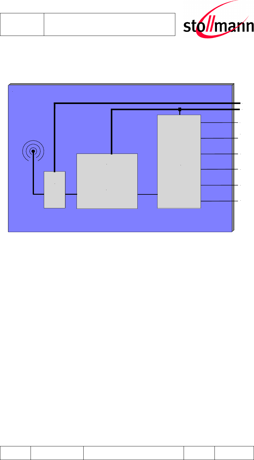
ARM7
CPU
AT91SAM7S
256k
FLASH
64k
SRAM
Bluetooth
BC04-ROM
+3V3
EXT-RES#
RS-232 (TTL)
BlueRS+C11/G2
Class1
PA
HCI
Single Chip
+3V3-PA
GPIO
USB 2.0 FS
JTAG
TEST
Fig. 1 Block Diagram
Stollmann
E + V GmbH
BlueMod+C11/G2
Hardware reference
Author: jj Date of Saving: 23.02.07 Ref: BlueRS+C11-G2_HWreference_V1_0.doc Revision: 0.1 Page 8 of 8
3 Application Interface
3.1 Power Supply
The BlueMod+C11/G2 has 2 power supply rails, which always should be kept on the
same voltage level.
Pin Signal Usage
C-13 3V3 Supply for digital and low power RF circuitry,
C-16 3V3-PA Supply for RF Amplifier
C-14 GND Reference Supply
C-15 GND Reference Supply
The pin order is made such that on the customer hardware directly at the pins of each
supply pair pins (C-13/C14) and pins (C-16/C-15) a 10uF X5R ceramic capacitor with for
example a 1206 footprint can be placed for decoupling. It is recommended to add further
smaller value ceramic capacitors. These values depend on noise frequencies on the
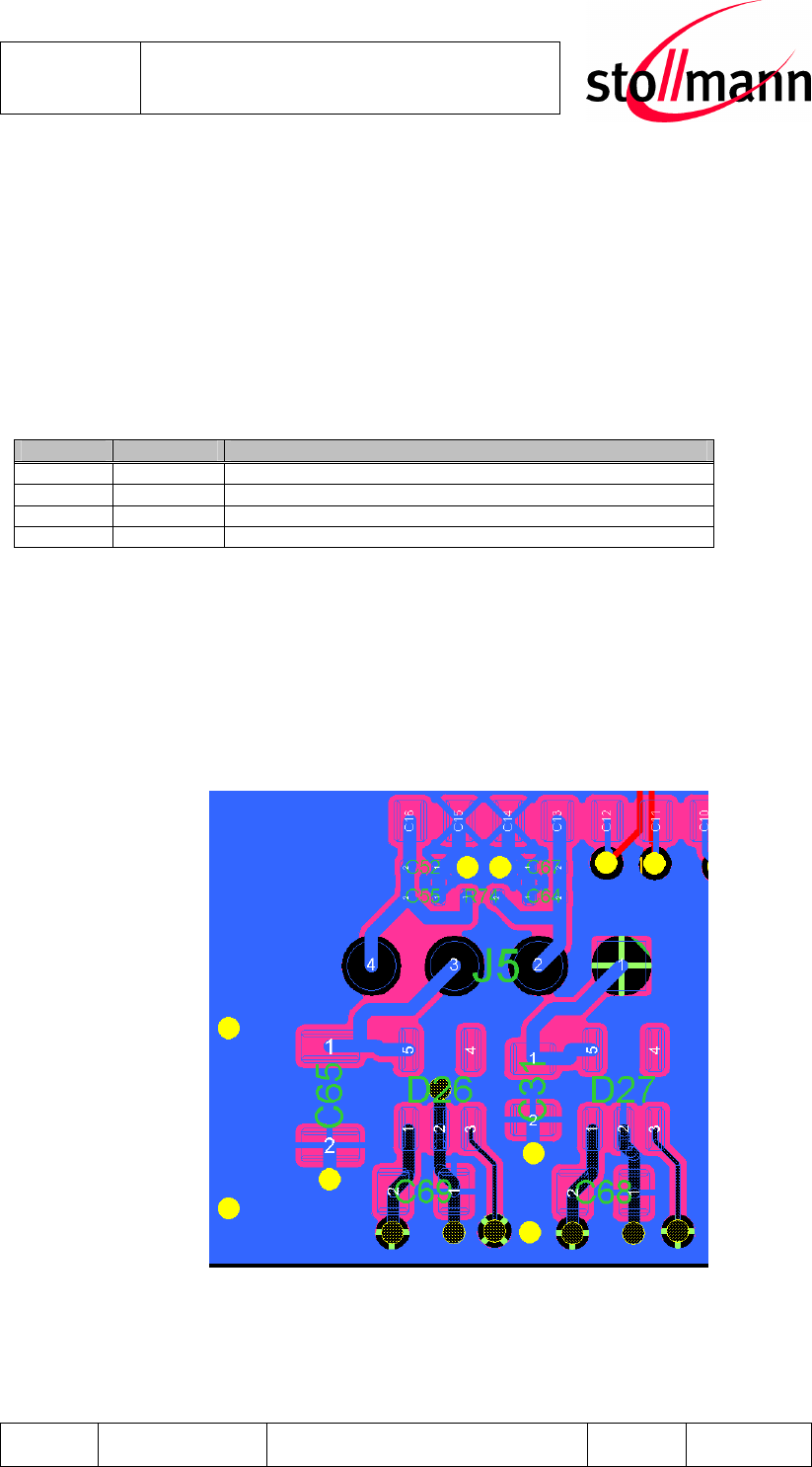
supply rail. The following picture shows a sample layout with 2 linear regulators in SOT23-
5 housings and various capacitors in SMT shapes 0402, 0805 and 1206.
Fig. 2 Sample Layout Power Supply
Each supply rail should be fed with 3,3V, Range 3,0V to 3,6V incl. Noise, low noise from a
linear regulator with fast transient response. Stollmann suggest using 2 pcs.
TOREX: XC6204B332MR

Stollmann
E + V GmbH
BlueMod+C11/G2
Hardware reference
Author: jj Date of Saving: 23.02.07 Ref: BlueRS+C11-G2_HWreference_V1_0.doc Revision: 0.1 Page 9 of 9
regulators, so that the fast current transients of the class1 RF power amplifier do not
interfere with sensitive PLL circuitry of the low power RF circuitry.
For layout guidelines please see sample implementation Stollmann reference design
BlueMod+Eval/C11/G2.
Excessive noise or too slow current transient response on the supply rails may have an
impact on the RF performance.
3.2 Power-On-Reset
The BlueMod+C11/G2 is equipped with circuitry for generating Power On Reset and to
provide under-voltage supervision. An integrated circuit type Maxim DS1818R provides
this functionality.
A reset is generated if the 3.3V supply rail including noise falls below 2,8V to 2,97V.
Via Pin A-1 an external reset can be generated by holding EXT-RES# at ≤ 0.3V for
≥ 10ms. A 74LVC14 Schmitt Trigger gate with a 1kR5/10nF low-pass filter at the input is
implemented to avoid false reset pulse recognition due to EMC effects.
If EXR-RES# is not used, it may be left open or tied to VCC.
Stollmann
E + V GmbH
BlueMod+C11/G2
Hardware reference
Author: jj Date of Saving: 23.02.07 Ref: BlueRS+C11-G2_HWreference_V1_0.doc Revision: 0.1 Page 10 of 10
3.3 Serial Interface
The interface functionally corresponds to the norm V.24 / RS-232 but has TTL-level.
• Transmission speeds 300 bps – 1,843200 Mbps (asynchronous)
• Character representation: 7 to 9 Bit, even, odd, mark, space or no Parity, 1, 1.5 or 2
stop bits
• Half duplex or full duplex
• Hardware flow-control (RTS/CTS)
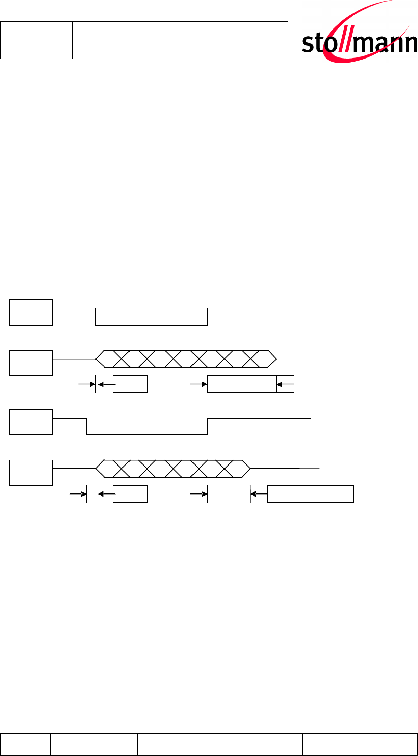
Note: All signals of the serial interface are named according to the EIA232 DTE definition.
CTS
Tbd
b
y
tes
max
Tbd
ns
TXD
RTS
Tbd
character max
Tbd
nS
RXD
Figure 1. UART Timing Diagram
3.4 GPIO Interface
All user signals, except for EXT-RES#, which is routed via a Schmitt Trigger gate, are
connected directly to port pins of the ATMEL AT91SAM7S256 CPU. Except for USB
signals DP, DM and GPIO(4), no pull-up or down resistors are implemented, so that the
I/O characteristics of the ATMEL CPU apply. These are
• 3V3 logic 5V tolerant
• V
IL
max = 0.8V, V
IH
min = 2.0V, V
IH
max = 5.5V
• V
OH
min = VCC – 0.4V @ I
O
= 8mA, V
OL
< 0.4V @ I
O
= 8mA
Stollmann
E + V GmbH
BlueMod+C11/G2
Hardware reference
Author: jj Date of Saving: 23.02.07 Ref: BlueRS+C11-G2_HWreference_V1_0.doc Revision: 0.1 Page 11 of 11
• LED’s can be driven directly on specific GPIO lines when I
o
stays below 8mA
All current consumption data in this document are given with I
O
(GPIO) = 0mA
See chapter 5 Electrical Characteristics for detailed information.
• All I/O signals except USB, GPIO(4) and JTAG are connected directly from the
AT91SAM7S pins to the user accessible stamp pins. Therefore the electrical
characteristics of the I/O pins are programmable in regard to direction, pull-up
resistor, function, push-pull or open drain. Please see specific application software
documentation for details. After reset all GPIO’s have pull-ups avtivated. GPIO10,
GPIO8 and TXD have 50kR to 300kR pull-ups, all other I/Os have 5kR to 20kR
pull-ups
3.5 Alternate GPIO/IO Functions
Application specificly dedicated GPIO or IO pins can be programmed to alternative
functionalities. Then pin functionality and direction are fixed for the activated function
block. Many GPIO’s or IO’s are used by the SPP application. See chapter SPP
Configuration. Probably some of them can be released for use by other function blocks.
Co-functionality of blocks has to be carefully considered, because pin multiplexing
possibilities are fixed by the ATMEL AT91SAM7S CPU and using a function block often
causes that other function blocks can’t be used at the same time. Please refer to the
ATMEL data sheet AT91SAM7Sxxx Rev. F for complete information. The possibilities
depicted in the following chapters are an subset only.
The following function blocks may be usable on the BlueMod+C11/G2:
3.5.1 Master/Slave SPI Interface
Direction Pin # GPIO#
IO Name
Alternative
Signal Name
Description
Master Slave
A5 GPIO1 MISO Master In Slave Out IN OUT
A4 GPIO0 MOSI Master Out Slave In OUT IN
A3 GPIO3 SPCK Serial Clock OUT IN
A6 GPIO2 NPCS0 Peripheral. Chip Select OUT IN
Clock polarity and phase are programmable. The chip select signal is low active.
Stollmann
E + V GmbH
BlueMod+C11/G2
Hardware reference
Author: jj Date of Saving: 23.02.07 Ref: BlueRS+C11-G2_HWreference_V1_0.doc Revision: 0.1 Page 12 of 12
3.5.2 Synchronous Serial Interface
The Synchonous Serial Interface is capable of handling the protocols I2S, Short Frame
Sync, Long Frame Sync and other Telecom protocols. Receiver and transmitter do act
independently. Due to multiplexing interdependencies the SSC is only available with the
Transmitter clock signal TK used for both directions if the UART IF is enabled. JTAG
reset, signal
/ATRST,
is also not available, if the SSC signal RF, Receiver Frame Sync is
used.
Direction Pin # GPIO#
IO Name
Alternative
Signal Name
Description
Case 1 Case 2
A16
/ATRST
RF Receiver Frame Sync IN OUT
A12 GPIO10 RD Receiver Data IN IN
C7 TXD RK Receiver Clock IN OUT
A13 GPIO7 TF Transmitter Frame Sync IN OUT
A11 GPIO8 TD Transmitter Data OUT OUT
A14 GPIO9 TK Transmitter Clock IN OUT
3.5.3 Multi Channel PWM Controller
Each PWM channel can be programmed individually in regard to IO pin assignment and
PWM functionality. Therefore PWM application designers can choose a proper channel
and pin for their application with the chance not to interfere with other necessary
interfaces.
Pin # GPIO#
IO Name
Alternative
Signal Name
Description Direction
A6 GPIO2 PWM0 PWM Waveform Out CH0 OUT
C9 GPIO5 PWM0 PWM Waveform Out CH0 OUT
C5 /CTS PWM1 PWM Waveform Out CH1 OUT
A5 GPIO1 PWM1 PWM Waveform Out CH1 OUT
A5 GPIO1 PWM1 PWM Waveform Out CH1 OUT
C2 GPIO15 PWM1 PWM Waveform Out CH1 OUT
C4 /RTS PWM2 PWM Waveform Out CH2 OUT
A4 GPIO1 PWM2 PWM Waveform Out CH2 OUT
C8 GPIO6 PWM2 PWM Waveform Out CH2 OUT
A3 GPIO3 PWM3 PWM Waveform Out CH3 OUT
Stollmann
E + V GmbH
BlueMod+C11/G2
Hardware reference
Author: jj Date of Saving: 23.02.07 Ref: BlueRS+C11-G2_HWreference_V1_0.doc Revision: 0.1 Page 13 of 13
3.5.4 PCM interface
XXX (JW)
For being able to use the PCM interface the HW needs to be altered. At the moment no
version with this alteration can be ordered. The PCB layout allows the use of the
Bluetooth HCI chips PCM interface at certain GPIO pins for future enhancements by
population changes. Then also the electrical characteristics of these pins do change,
because the characteristics of the CSR BC04 Bluetooth HCI chip apply. Especially the 5V
IO tolerance is not applicable anymore.
Pin # GPIO#
IO Name
Alternative
Signal Name
Description Direction
A12 GPIO10
PCM-OUT
PCM Data Out OUT
A11 GPIO8
PCM-IN
PCM Data In IN
A14 GPIO9 PCM-CLK PCM Clock OUT ???
A13 GPIO7 PCM-SYNC PCM Frame Sync OUT ???
PCM-Out has a 10k pull-up to +3V3 and is driven OC only.
The following electrical characteristics apply:
Input Voltage Levels Min Max
V
IL
- 0.4V +0.8V
V
IH
0.7 VCC VCC + 0.4V
Output Voltage Level
V
OL
(I
O
< 4mA sunk) 0.2V
V
OH
(I
O
< 4mA sourced) VDD-0.2V
3.5.5 Analog to Digital Converter
3 ADC channels with 8 to 10bit resolution in reference to 1.8V are available. A wide range
of trigger sources and programmable S&H timing are available.
Pin # GPIO#
IO Name
Alternative
Signal Name
Description Direction
A16 JTAG-RES#
AD3
ADC channel 3 In analogue
A12 GPIO10
AD0
ADC channel 0 In analogue
A11 GPIO8 AD1 ADC channel 1 In analogue

Stollmann
E + V GmbH
BlueMod+C11/G2
Hardware reference
Author: jj Date of Saving: 23.02.07 Ref: BlueRS+C11-G2_HWreference_V1_0.doc Revision: 0.1 Page 14 of 14
3.6 Bluetooth radio Interface
The BlueMod+C11/G2 offers 3 population variants for the antenna
1) The BlueMod+C11/G2/-AE variant presents a 50Ω impedance antenna interface on a
Radiall UMP connector, type R107103020. See http://www.radiall.com/
2) The BlueMod+C11/G2/-AI variant presents an integrated ceramic antenna.
3) The BlueMod+C11/G2/-AP variant presents a 50Ω impedance antenna interface on pin
A-27 with adjacent GND pins A-26 and A-28. Signal routing of the RF signal on customer
PCB has to be implemented with 50R micro-strip line technique.
Pins A-26 and A-28 should be connected directly to the reference GND plane.
If the antenna performance does not meet your requirements or you need antenna
support, please contact Stollmann.
3.7 Etc.
For SW development purposes on the module pins a full JTAG interface connected to the
ATMEL CPU is implemented.
Stollmann
E + V GmbH
BlueMod+C11/G2
Hardware reference
Author: jj Date of Saving: 23.02.07 Ref: BlueRS+C11-G2_HWreference_V1_0.doc Revision: 0.1 Page 15 of 15
4 Pin Description
The BlueMod+C11/G2 module is soldered on customers PCB via stamp pins located on
the module PCB edges.
4.1 Pin Numbering
Top View
Stollmann
E + V GmbH
BlueMod+C11/G2
Hardware reference
Author: jj Date of Saving: 23.02.07 Ref: BlueRS+C11-G2_HWreference_V1_0.doc Revision: 0.1 Page 16 of 16
4.2 Pin Description
4.2.1 General Pin Description
Pin Signal Dir.
Activ
Description
A1 /EXT_RES I L Reset low active
A2 M0-DTXD I Test pin – do not connect
A3 GPIO3 () I/O General Purpose IO
A4 GPIO0 () I/O General Purpose IO
A5 GPIO1 () I/O General Purpose IO
A6 GPIO2 () I/O General Purpose IO
A7 ATDO
O JTAG test data output
A8 ATCK I JTAG clock
A9 ATMS I JTAG mode select
A10 ATDI I JTAG test data input
A11 GPIO8 (PCM_IN) I General Purpose IO
A12 GPIO10 (PCM_OUT) O General Purpose IO
A13 GPIO7 (PCM_SYNC) O General Purpose IO
A14 GPIO9 (PCM_CLK) O General Purpose IO
A15 M1-DRXD I Test pin – do not connect
A16 /ATRST I L GPIO or JTAG reset (Pop Change nec.)
A17 TST I Test pin – do not connect (SAMBA = HIGH)
A26 ANT_GND Antenna ground, connect directly to plane
A27 ANT 50 Ohm Rx/Tx connection to antenna
A28 ANT_GND Antenna ground, connect directly to plane
C1 GPIO14 I/O General Purpose IO
C2 GPIO15 I/O General Purpose IO (SAMBA = HIGH)
C3 GPIO13 I/O General Purpose IO
C4 /RTS I L Request to send
C5 /CTS O L Clear to send
C6 RXD O Receive Data
C7 TXD I Transmit Data
C8 GPIO6 I/O General Purpose IO (SAMBA = HIGH)
C9 GPIO5 I/O General Purpose IO (SAMBA = HIGH)
C10 GPIO4 I/O General Purpose IO
C11 USB_DM I/O USB D-, Data pin
C12 USB_DP I/O USB D+, Data pin
C13 VCC P +3.3V Power digital and low power RF
C14 GND P GND
C15 GND P GND
C16 VCC P +3.3V Power RF amplifier
Stollmann
E + V GmbH
BlueMod+C11/G2
Hardware reference
Author: jj Date of Saving: 23.02.07 Ref: BlueRS+C11-G2_HWreference_V1_0.doc Revision: 0.1 Page 17 of 17
4.2.2 Application Specific Pin Description
4.2.3 SPP Configuration
Pin Pin Name SPP function
Dir. Active Description
A3 GPIO3 Break out O tbd generate break
A4 GPIO0 I/O
A5 GPIO1 Break detect I Optional, connect external to RXD
special firmware required
A6 GPIO2 I/O General Purpose IO
A11 GPIO8 ID1 O Identification signal 1
A12 GPIO10 UA2 O User Output 2
A13 GPIO7 /LED1 O L
Device ready
A14 GPIO9 /LED2 O L
Bluetooth connected. Active if a
Bluetooth connection exists.
Inactive in idle state. Flashes
during startup.
C1 GPIO14 /RTC-OUT O L DSR in DCE mode DTR in DTE mode
C2 GPIO15 /DCD I/O L Data Carrier Detect input in DTE
mode, output in DCE mode
C3 GPIO13 /RTC-IN I L DTR in DCE mode DSR in DTE mode
C4 /RTS I L Request to send
C5 /CTS O L Clear to send
C6 RXD O Receive Data
C7 TXD I Transmit Data
C8 GPIO6 /RI I/O Ring Indicator input in DTE mode,
output in DCE mode
C9 GPIO5 ID2 O Identification signal 2
C10 GPIO4 DTE-/DCE I 10k PD DTE DCE mode selector
C13 VCC VCC P +3.3V Power
C14
GND
GND P
GND
C15
GND
GND P
GND
C16
VCC
VCC P
+3.3V Power
A1 /EXT_RES /EXT_RES I
L Reset low active
C11 USB_DM
Do not connect
C12
USB_DP
Do not connect

Stollmann
E + V GmbH
BlueMod+C11/G2
Hardware reference
Author: jj Date of Saving: 23.02.07 Ref: BlueRS+C11-G2_HWreference_V1_0.doc Revision: 0.1 Page 18 of 18
5 Electrical Characteristics
5.1 Absolute Maximum Ratings
Stresses beyond those listed under “Absolute Maximum Ratings” may cause permanent
damage to the device. These are stress ratings only, and functional operation of the
device at these or any other conditions beyond those indicated under “Electrical
Requirements” is not implied. Exposure to absolute-maximum-rated conditions for
extended periods may affect device reliability.
Item Symbol Absolute Maximum Ratings Unit
Supply voltage V
cc
3,7V with respect to GND to
- 0,4V with respect to GND V
Voltage on any pin V
Pin
VCC + 0,4V with respect to GND to
- 0,4V with respect to GND V
Input RF level P
max
0 dBm
ESD on any pin V
ESD
This device is ESD sensitive. Handling and assembly
of this device should be at ESD protected
workstations
.
5.2 Operating Conditions
5.2.1 RF and Supply Connections
Vcc = 3.0V to 3.6V, T
amb
= - 40°C to +85°C
Item Condition Limit Unit
Min Typ Max
Frequency Range
Pin A-27 2400 2483.5 MHz
Load impedance
Pin A-27 or
UMP connector
Measured with network analyzer in
the frequency range at antenna pin
50 Ω
Output return loss
Pin A-27 or
UMP connector
Receive Mode to 50Ω load
Transmit Mode to 50Ω load
-10
-10 dBm
Supply voltage
Pin C-13 and
Pin C-16
The typical voltage is
recommended Vcc at voltage pin
(incl. ripple) 3.0 3.3 3.6 Vdc
Ripple on Vcc Ripple frequency ≥200kHz
Ripple frequency <200kHz 20
20 mVrms
Stollmann
E + V GmbH
BlueMod+C11/G2
Hardware reference
Author: jj Date of Saving: 23.02.07 Ref: BlueRS+C11-G2_HWreference_V1_0.doc Revision: 0.1 Page 19 of 19
5.2.2 GPIO, JTAG; Serial IF and Test Pins
Vcc = 3.3V, T
amb
= - 40°C to +85°C
Symbol Item Condition Limit Unit
Min Max
V
IL
Low-Level Input Voltage -0.3 0.8 V
V
IH
High-Level Input Voltage 2.0 5.5 V
V
OL
Low-Level Output Voltage I
OL
< 8mA
-
0.4
V
V
OH
High-Level Output Voltage I
OH
< 8mA
VCC-0.4 - V
I
O1
Output Current
GPIO(5,6,15) - 16 mA
I
O2
Output Current
GPIO(10,8), TXD,
/JTAG-RES - 2 mA
I
O3
Output Current
Other PIO
except USB 8
Note: Please refer to ATMEL AT91SAM7S data sheet for more specific information
5.2.3 USB Pins
Vcc = 3.3V, T
amb
= - 40°C to +85°C
Symbol Item Condition Limit Unit
Min Max
V
IL
Low-Level Input Voltage 0.8 V
V
IH
High-Level Input Voltage 2.0 V
V
DI
Diff. Input Sensitivity 0.2 V
V
CM
Common Mode Range 0.8 2.5 V
V
OL
Low-Level Output Voltage R
L
= 1.425k to 3V6
0.0 0.3
V
V
OH
High-Level Output Voltage R
L
= 14.25k to GND
2.8 3.6- V

Stollmann
E + V GmbH
BlueMod+C11/G2
Hardware reference
Author: jj Date of Saving: 23.02.07 Ref: BlueRS+C11-G2_HWreference_V1_0.doc Revision: 0.1 Page 20 of 20
5.3 Power consumption and power down modes
To reduce power consumption of the BlueMod+C11/G2 power down modes can be
activated automatically by the BlueMod+C11/G2 (controlled by parameter settings).
If no Bluetooth connection is established, the following states are implemented, the
activation of these states can be controlled by the parameters bpsm and pwd.
For more details please refer to the BlueMod+C11/G2 software manual.
5.3.1 SPP configuration
5.3.1.1 Deep Sleep state
The Bluetooth RF is completely deactivated, no paging requests from other Bluetooth
devices will be recognized. Only rising control line DTR will activate the BlueMod+C11/G2
and may initiate a Bluetooth link dependent on other parameters.
Note: In Deep Sleep state the AT command set is not active, CTS line is low
5.3.1.2 Power down state
The Bluetooth RF is activated every 1.25 seconds, paging requests from other Bluetooth
devices will be recognized after that intervals and accepted if allowed. Additionally rising
control line DTR will activate the BlueMod+C11/G2 and may initiate a Bluetooth link
dependent on other parameters.
Note: In Power down state the AT command set is not active, CTS line is low
5.3.1.3 Idle state
The Bluetooth RF is activated every 1.25 seconds, paging requests from other Bluetooth
devices will be recognized after that intervals and accepted if allowed. Additionally rising
control line DTR will activate the BlueMod+C11/G2 and may initiate a Bluetooth link
dependent on other parameters
Stollmann
E + V GmbH
BlueMod+C11/G2
Hardware reference
Author: jj Date of Saving: 23.02.07 Ref: BlueRS+C11-G2_HWreference_V1_0.doc Revision: 0.1 Page 21 of 21
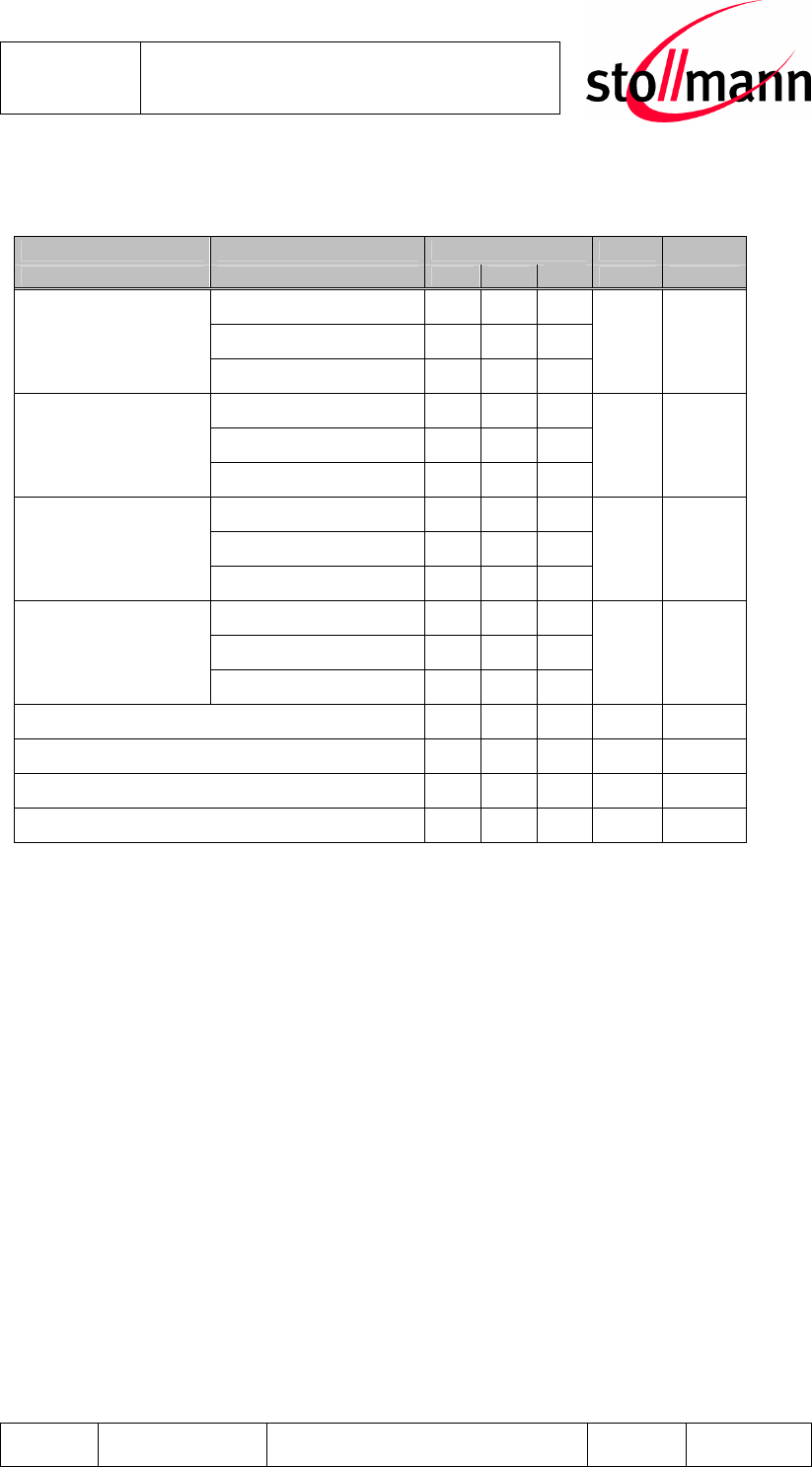
5.3.1.4 Power Consumption
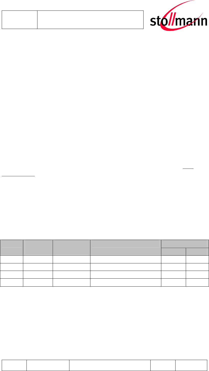
Condition Current Consumption
I
MEAN
/mA I
PEAK
/mA
Deep sleep tbd
tbd
Power down tbd
tbd
Idle, all functions available, no Bluetooth link tbd
tbd
Page Scan 12,1
101,0
Inquiry and Page Scan 12,4
101,0
Bluetooth connected, no data traffic, max. TX PWR (Slave) 34,7
185,0
ACL connected DH5 max PWR, shortest Poll Period (Slave) 133,3
175,0
ACL connected DH5 min PWR, shortest Poll Period (Slave) 57,5
99,0
ACL connected DH1 max PWR, shortest Poll Period (Slave) 59,0
175,0
ACL connected DH1 min PWR, shortest Poll Period (Slave) 55,0
110,0
Note: Table to be extended after further measurements
Fig. 3: MEASURMENT SET UP
Stollmann
E + V GmbH
BlueMod+C11/G2
Hardware reference
Author: jj Date of Saving: 23.02.07 Ref: BlueRS+C11-G2_HWreference_V1_0.doc Revision: 0.1 Page 22 of 22
5.4 RF performance
Vcc = 3.0V to 3.6V, T
amb
= - 40°C to +85°C
Receiver Frequency [GHz] Limit BT Unit
Min Typ Max Spec
2.402 -90,0 -80,0
2.441 -90,0 -80,0
Sensitivity at 0.1% BER
DH1
2.480 -90,0 -80,0
≤-70 dBm
2.402 -90,0 -80,0
2.441 -90,0 -80,0
Sensitivity at 0.1% BER
DH5
2.480 -90,0 -80,0
≤-70 dBm
2.402 -88,0 -80,0
2.441 -88,0 -80,0
Sensitivity at 0.1% BER
PI/4 DQPSK
2.480 -88,0 -80,0
≤-70 dBm
2.402 -82,0 -74,0
2.441 -82,0 -74,0
Sensitivity at 0.1% BER
8DPSK
2.480 -82,0 -74,0
≤-70 dBm
Maximum received signal at 0.1% BER with DH1 -20,0 >10 ≥-20 dBm
Maximum received signal at 0.1% BER with DH5 -20,0 >10 ≥-20 dBm
Maximum received signal at 0.1% BER with PI/4 DQPSK -20,0 -12,0 ≥-20 dBm
Maximum received signal at 0.1% BER with 8DPSK -20,0 -18,0 ≥-20 dBm
Stollmann
E + V GmbH
BlueMod+C11/G2
Hardware reference
Author: jj Date of Saving: 23.02.07 Ref: BlueRS+C11-G2_HWreference_V1_0.doc Revision: 0.1 Page 23 of 23
Vcc = 3.0V to 3.6V, Tamb = - 40°C to +85°C
Transmitter Frequency [GHz] Limit BT Unit
Min Typ Max Spec
2.402 16,0 18,5 19,0
2.441 16,0 18,5 19,0
RF transmit power
50 Ω load, at antenna
Class 1 device GFSK
a)
2.480 16,0 18,5 19,0
+4 to
+20 dBm
2.402 tbd
2.441 tbd
RF transmit power
50 Ω load, at antenna
Class 1 device EDR2
a)
2.480 tbd
2.402 tbd
2.441
tbd
RF transmit power
50 Ω load, at antenna
Class 1 device EDR3
a)
2.480 tbd
RF power control range 17 dB
RF power range control resolution 4 2 to 8 dB
20 dB bandwidth for modulated carrier 780 1000 ≤1000 kHz
Initial carrier frequency tolerance 5 30 ≤ ±75 kHz
Carrier frequency drift (packet DH1) 7 25 ≤ ±25 kHz
Drift Rate 6 20 20 kHz/ 50µs
∆f1
avg
“Maximum Modulation” 140 165 175 ≥140 to
≤175 kHz
∆f2
avg
“Minimum Modulation” 115 154 ≥ 115 kHz
C/I co-channel
b)
8 11 ≤ 11 dB
Adjacent channel selectivity C/I f = f
0
+ 1MHz
b)
-6 0 ≤ 0 dB
Adjacent channel selectivity C/I f = f
0
- 1MHz
b)
-4 0 ≤ 0 dB
Adjacent channel selectivity C/I f ≥ f
0
+ 2MHz
b)
-38 -30 ≤ -30 dB
Adjacent channel selectivity C/I f ≤ f
0
- 2MHz
b)
-24 -20 ≤ -30 dB
Adjacent channel selectivity C/I f ≥ f
0
+ 3MHz
b)
-45 -40 ≤ -40 dB
Adjacent channel selectivity C/I f ≤ f
0
- 5MHz
b)
-45 -40 ≤ -40 dB
Adjacent channel selectivity C/I f = f
image
b)
-21 -9 ≤ -9 dB
Notes: a) Including +2dBi antenna gain
b) Applies according to BT Test Specification Ver. 1.2/2.0/2.0 + EDR only for Tamb = 20°C
Stollmann
E + V GmbH
BlueMod+C11/G2
Hardware reference
Author: jj Date of Saving: 23.02.07 Ref: BlueRS+C11-G2_HWreference_V1_0.doc Revision: 0.1 Page 24 of 24
Enviromental Requirements
Item Symbol Absolute Maximum Ratings Unit
Storage temperature range T
stg
-40 to +105 °C
Operating temperature range T
op
-40 to +85 °C
5.5 Power-up Time
The time until the BlueMod+C11/G2 is able to accept link requests or serial data is about
TBD seconds after power-up. This time can be reduced to approx. tbd second by
parameter change.
Stollmann
E + V GmbH
BlueMod+C11/G2
Hardware reference
Author: jj Date of Saving: 23.02.07 Ref: BlueRS+C11-G2_HWreference_V1_0.doc Revision: 0.1 Page 25 of 25
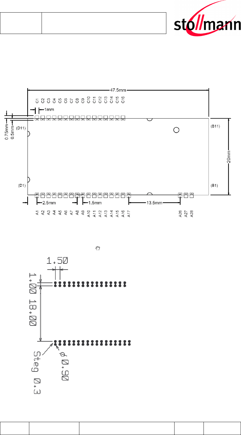
6 Mechanical Characteristics
6.1 Dimensions
6.2 Connectors
Except for the stamp pins A-[1-17,26-28] and C-[1-16] and the UMP antenna connector no
user accessible connectors are implemented.
If the use of the UMP antenna connector is considered, please contact Stollmann for
information on accessories like cables, plugs etc. Or look at www.radiall.com for the UMP
type family. On the BlueMod+C11/G2 the following receptacle will be populated for RF
signal routing, if the BlueMod+C11/G2/-AE variant is ordered.
Manufacturer Type
Radiall RADIALL: R107103020 UMP connector receptable
Stollmann
E + V GmbH
BlueMod+C11/G2
Hardware reference
Author: jj Date of Saving: 23.02.07 Ref: BlueRS+C11-G2_HWreference_V1_0.doc Revision: 0.1 Page 26 of 26
6.3 Recommended Land Pattern
Land pattern recommended for manual soldering
Alternative land pattern recommended for reflow soldering

Stollmann
E + V GmbH
BlueMod+C11/G2
Hardware reference
Author: jj Date of Saving: 23.02.07 Ref: BlueRS+C11-G2_HWreference_V1_0.doc Revision: 0.1 Page 27 of 27
6.4 Housing Guidelines
The individual case must be checked to decide whether a specific housing is suitable for
the use of the internal antenna. A plastic housing must at least fulfill the following
requirements:
• Non-conductive material, non-RF-blocking plastics
• No metallic coating
• ABS is suggested
Stollmann
E + V GmbH
BlueMod+C11/G2
Hardware reference
Author: jj Date of Saving: 23.02.07 Ref: BlueRS+C11-G2_HWreference_V1_0.doc Revision: 0.1 Page 28 of 28
6.5 Antenna Issues
BlueMod+C11/G2 is shipped with 3 different antenna designs:
• BlueMod+C11/G2/-AI comprises a ceramic antenna which as a component is soldered
to the circuit board. This is functional for a BlueMod+C11/G2/-AI integrated into a
plastic housing. No additional antenna is required.
For an external antenna to be set in, e.g. because the BlueMod+C11/G2 is integrated into
a metal housing, the ceramic antenna is replaced by 2 alternative solutions
• BlueMod+C11/G2/-AE has a UMP connector (50 Ohm technology) populated as
Antenna Interface
• BlueMod+C11/G21/-AP routes the antenna signal to pin A27.
The gain of the external antenna shall not exceed +2dB
i
.
When using an external Antenna the antenna is fixed and cannot be removed or replaced
by the end user. The performance of the internal antenna respectively the external
antenna has in any case to be checked within the final integration environment. Adjacent
PCBs, components, cables, housings etc. could otherwise influence the radiation pattern
or be influenced by the radio wave energy.
It must be ensured that the antenna is not co-located or operating in conjunction with any
other antennas, transmitters, cables or connectors. When the internal ceramic antenna is
used, certain restrictions are to be considered.
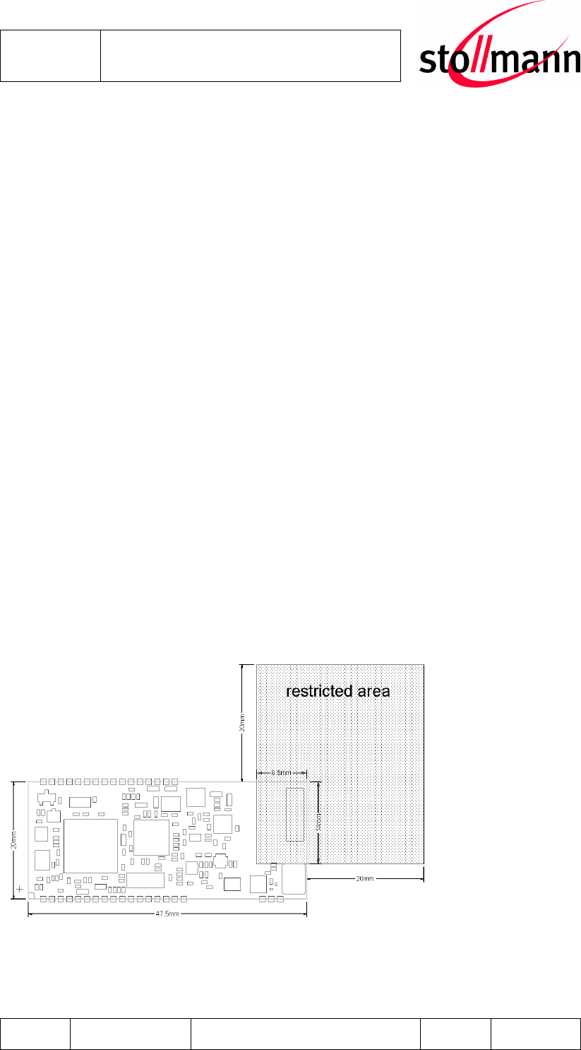
Antenna – recommended restricted area
Stollmann
E + V GmbH
BlueMod+C11/G2
Hardware reference
Author: jj Date of Saving: 23.02.07 Ref: BlueRS+C11-G2_HWreference_V1_0.doc Revision: 0.1 Page 29 of 29
To give an optimized antenna performance the restricted area having no ground or power
planes, traces or parts should be widened. The following dimensions should be
implemented, depending on your possible space.
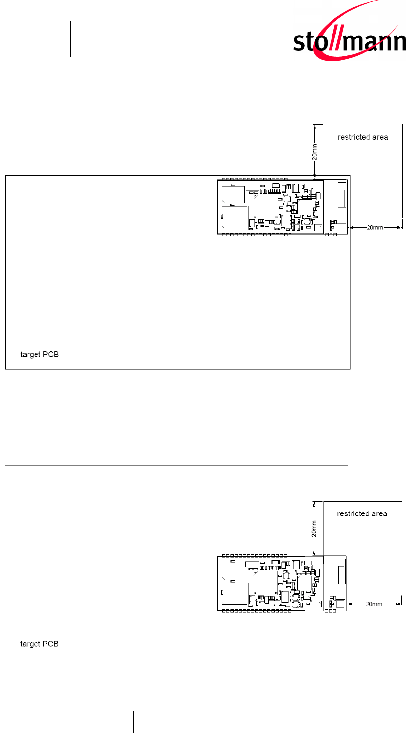
Optimal placement
The best position to place the BlueMod+C11/G2 on the target PCB is in the upper right
corner. This position is optimal concerning antenna interference; radiation pattern and
PCB space that has to be keep free for the restricted area.
recomendable placement
Stollmann
E + V GmbH
BlueMod+C11/G2
Hardware reference
Author: jj Date of Saving: 23.02.07 Ref: BlueRS+C11-G2_HWreference_V1_0.doc Revision: 0.1 Page 30 of 30
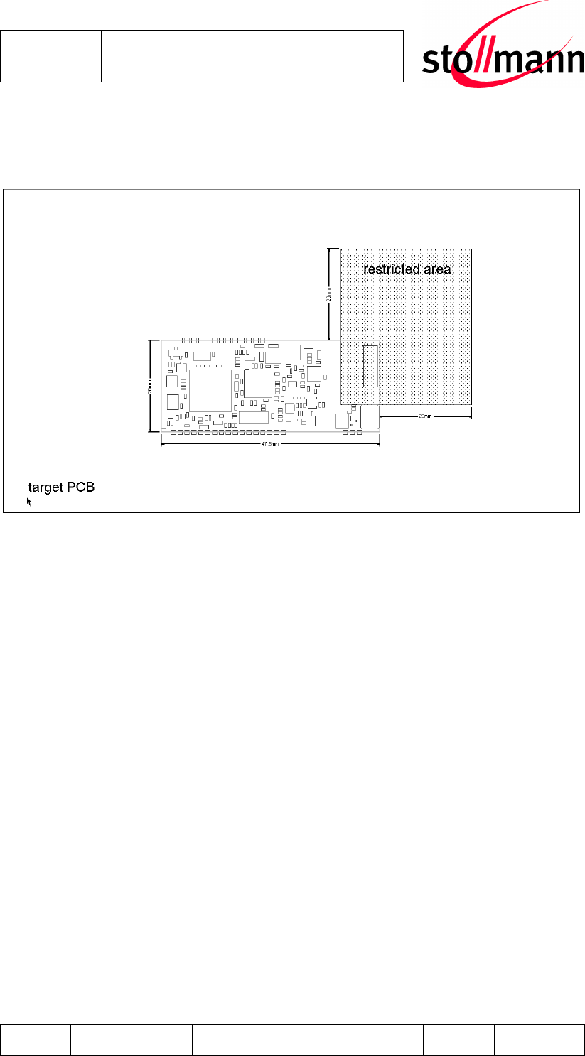
When placing the BlueMod+C11/G2 at the right edge of the PCB ensure that the restricted
area on the target PCB is free of planes, traces and parts.
acceptable, but not optimal placement
When placing the BlueMod+C11/G2 on other positions than the right side the complete
restricted area should be kept free of planes, traces and parts.

Stollmann
E + V GmbH
BlueMod+C11/G2
Hardware reference
Author: jj Date of Saving: 23.02.07 Ref: BlueRS+C11-G2_HWreference_V1_0.doc Revision: 0.1 Page 31 of 31
7 Safety Guidelines
According to SAR regulation EN 50371-2002 the BlueMod+C11/G2 is not intended to be
used in close proximity to the human body. Please refer to above-mentioned regulation for
more specific information.
In respect to the safety regulation EN 60950-1: 2001 all conductive parts of the
BlueMod+C11 are to be classified as SELV circuitry. OEM’s implementing the
BlueMod+C11/G2 in their products should follow the isolation rules given in regulation
EN 60950-1: 2001.
The PCB material of the BlueMod+C11/G2 is classified UL-94V0.
8 Regulatory Information
8.1 Declaration of conformity
Declaration of Conformity in accordance with Radio and Telecommunications Terminal
Equipment Act (FTEG) and Directive 1999/5/EC (R&TTE Directive
Stollmann E+V GmbH, Mendelssohnstr. 15d, D-22761 Hamburg, Jens Jensen
The manufacturer / responsible person
declares that the product family
BlueMod+C11/G2
Telecommunications terminal equipment with intended purpose: Serial Bluetooth Module
complies with the essential requirements of §3 and the other relevant provisions of the FTEG ( Article 3 of the R&TTE
Directive), when used for its intended purpose.
Health and safety requirements pursuant to §3(1)1.(Article 3(1)a))
:
Average Output Power is lower than 20mW, not intended to be used close to the human body.
Harmonised standards applied
EN 60 950-1: 2001, EN 50371-2002
Protection requirements concerning electromagnetic compatibility §3(1)(2), (Article 3(1)b))
harmonised standards applied
EN 301 489-1 V1.5.1
(tested mounted on Blue+EVA built in plastic housing)
EN 301 489-17 V1.2.1
(tested mounted on Blue+EVA built in plastic housing)
EN 300 328-2 V1.6.1 (2004)
(tested mounted on Blue+EVA built in plastic housing)
Electromagnetic compatibility and Radio Spectrum Matters (ERM)
Original signed available on request

Stollmann
E + V GmbH
BlueMod+C11/G2
Hardware reference
Author: jj Date of Saving: 23.02.07 Ref: BlueRS+C11-G2_HWreference_V1_0.doc Revision: 0.1 Page 32 of 32
8.1.1 FCC Compliance and FCC Statement
This device complies with Part 15 of the FCC Rules and with RSS-210 of Industry
Canada.
Operation is subject to the following two conditions:
(1) This device may not cause harmful interference, and
(2) This device must accept any interference received, including interference that
may cause undesired operation.
8.1.2 Caution
Warning: Changes or modifications made to this equipment not expressly approved by
Stollmann Entwicklungs und Vertriebs GmbH may void the FCC authorization to operate
this equipment.
8.1.3 FCC Warning
This equipment has been tested and found to comply with the limits for a Class B digital
device, pursuant to Part 15 of the FCC Rules. These limits are designed to provide
reasonable protection against harmful interference in a residential installation. This
equipment generates, uses and can radiate radio frequency energy and, if not installed
and used in accordance with the instructions, may cause harmful interference to radio
communications. However, there is no guarantee that interference will not occur in a
particular installation. If this equipment does cause harmful interference to radio or
television reception, which can be determined by turning the equipment off and on, the
user is encouraged to try to correct the interference by one or more of the following
measures:
• Reorient or relocate the receiving antenna.
• Increase the separation between the equipment and receiver.
• Connect the equipment into an outlet on a circuit different from that to which the
receiver is connected.
Consult the dealer or an experienced radio/TV technician for help.
The radiated output power of BlueMod+C11/G2 is far below the FCC radio frequency
exposure limits. Nevertheless, the BlueMod+C11/G2 shall be used in such a manner, that
the potential for human contact during normal operation is minimized.

Stollmann
E + V GmbH
BlueMod+C11/G2
Hardware reference
Author: jj Date of Saving: 23.02.07 Ref: BlueRS+C11-G2_HWreference_V1_0.doc Revision: 0.1 Page 33 of 33
8.1.4 RF-exposure Statement
The BlueMod+C11/G2 contains a portable modular transmitter. Thus it must have a
separation of at least 2.5 cm between the antenna and the body of the user or nearby
persons, excluding hands, wrists, feet, and ankles.
Any notification to the end user of installation or removal instructions about the integrated
radio module is not allowed.
8.1.5 Labelling and re-test requirements for the End Product
Any End Product integrating the BlueMod+C11/G2 must be labeled with at least the
following information:
This device contains transmitter with
FCCID: RFR- C11G2
IC ID: 4957A-C11G2
Since the BlueMod+C11/G2 is a module to be integrated into a for the FCC authority
unknown end product, the FCC approval under this ID is a “Limited Modular Approval”,
also called LMO. This implies that all OEM’s incorporating the BlueMod+C11/G2 in their
end product and wanting to ship to the USA or Canada have to measure spurious
emissions according to FCC Part 15.247 in a FCC accredited EMC lab and have to keep
the test report in their technical compliance folder ready for being checked by US/CA
market authorities.
8.2 Bluetooth Qualification
This product uses a Bluetooth qualified end product with Bluetooth
QD ID (Qualified Design Identifier) B012419

Stollmann
E + V GmbH
BlueMod+C11/G2
Hardware reference
Author: jj Date of Saving: 23.02.07 Ref: BlueRS+C11-G2_HWreference_V1_0.doc Revision: 0.1 Page 34 of 34
8.3 RoHS Declaration
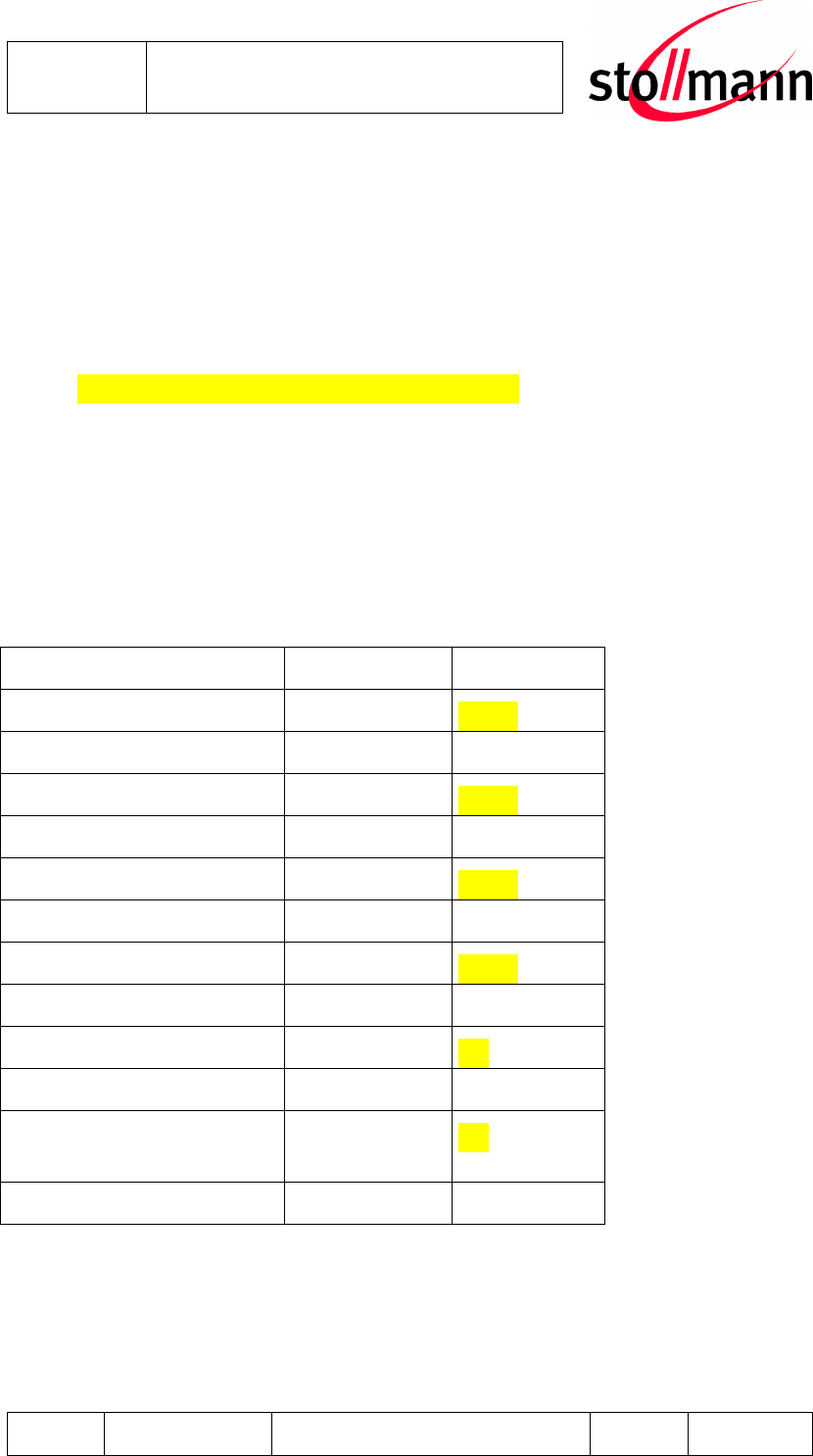
Declaration of environmental compatibility for supplied products:
Hereby we declare to our best present knowledge based on declaration of our suppliers that this product do not contain by
now the following substances which are banned by Directive 2002/95/EC (RoHS) or if contain a maximum concentration
of 0,1% by weight in homogeneous materials for
• Lead and lead compounds
• Mercury and mercury compounds
• Chromium (VI)
• PBB (polybrominated biphenyl) category
• PBDE (polybrominated biphenyl ether) category
And a maximum concentration of 0,01% by weight in homogeneous materials forCadmium and cadmium compounds
Stollmann
E + V GmbH
BlueMod+C11/G2
Hardware reference
Author: jj Date of Saving: 23.02.07 Ref: BlueRS+C11-G2_HWreference_V1_0.doc Revision: 0.1 Page 35 of 35
9 Related Documents
• ATMEL data sheet AT91SAM7Sxxx Rev. F
• CSR product data book BlueCore
TM
4-ROM BC41B143A April 2006
• Radiall UMP MMP Introduction
• Radiall data sheet UMP R107.103.020
• Stollmann BlueMod+C11/G2 Software Manual
• Bluetooth SIG RF_TS_EDR.pdf test specification
•
10 Ordering Information
The BlueRS+C11/G2 is available in the following variants:
Name Antenna Art No.
BlueMod+C11/G2/AI/SPP Internal 52672
…/EDR
BlueMod+C11/G2/AE/SPP External 52733
…/EDR
BlueMod+C11/G2/AI/SMA 52715
…/EDR
BlueMod+C11/G2/AI/SMA 52731
…/EDR
BlueMod+C11/G2/AP/SPP External tbd
…/EDR
BlueEva+C11/G2,
Evaluation Kit
Internal tbd
…/EDR
11 Life Support Policy
This Stollmann product is not designed for use in life support appliances, devices, or systems where malfunction can
reasonably be expected to result in a significant personal injury to the user, or as a critical component in any life support
device or system whose failure to perform can be reasonably expected to cause the failure of the life support device or

Stollmann
E + V GmbH
BlueMod+C11/G2
Hardware reference
Author: jj Date of Saving: 23.02.07 Ref: BlueRS+C11-G2_HWreference_V1_0.doc Revision: 0.1 Page 36 of 36
system, or to affect its safety or effectiveness. Stollmann customers using or selling these products for use in such
applications do so at their own risk and agree to fully indemnify Stollmann for any damages resulting.

Stollmann
E + V GmbH
BlueMod+C11/G2
Hardware reference
Author: jj Date of Saving: 23.02.07 Ref: BlueRS+C11-G2_HWreference_V1_0.doc Revision: 0.1 Page 37 of 37
12 History
Version Release Date By
Change description
0.1 20.10.2006 JJ Initial Document - preliminary
0.2 27.10.2006 JJ Updated Alternative GPIO Functionality,
Name correction
1.0 20.02.2007 JJ Updated to evaluated data