Texas Instruments 26M1 BLE and 802.15.4 module User Manual
Texas Instruments Inc. BLE and 802.15.4 module Users Manual
UserManual.wiki
>
Texas Instruments
>
26M1 User Manual
Users Manual
Navigation menu
Upload a User Manual
Namespaces
Wiki Guide
HTML
PDF
Info
Views
User Manual
Discussion / Help
Navigation
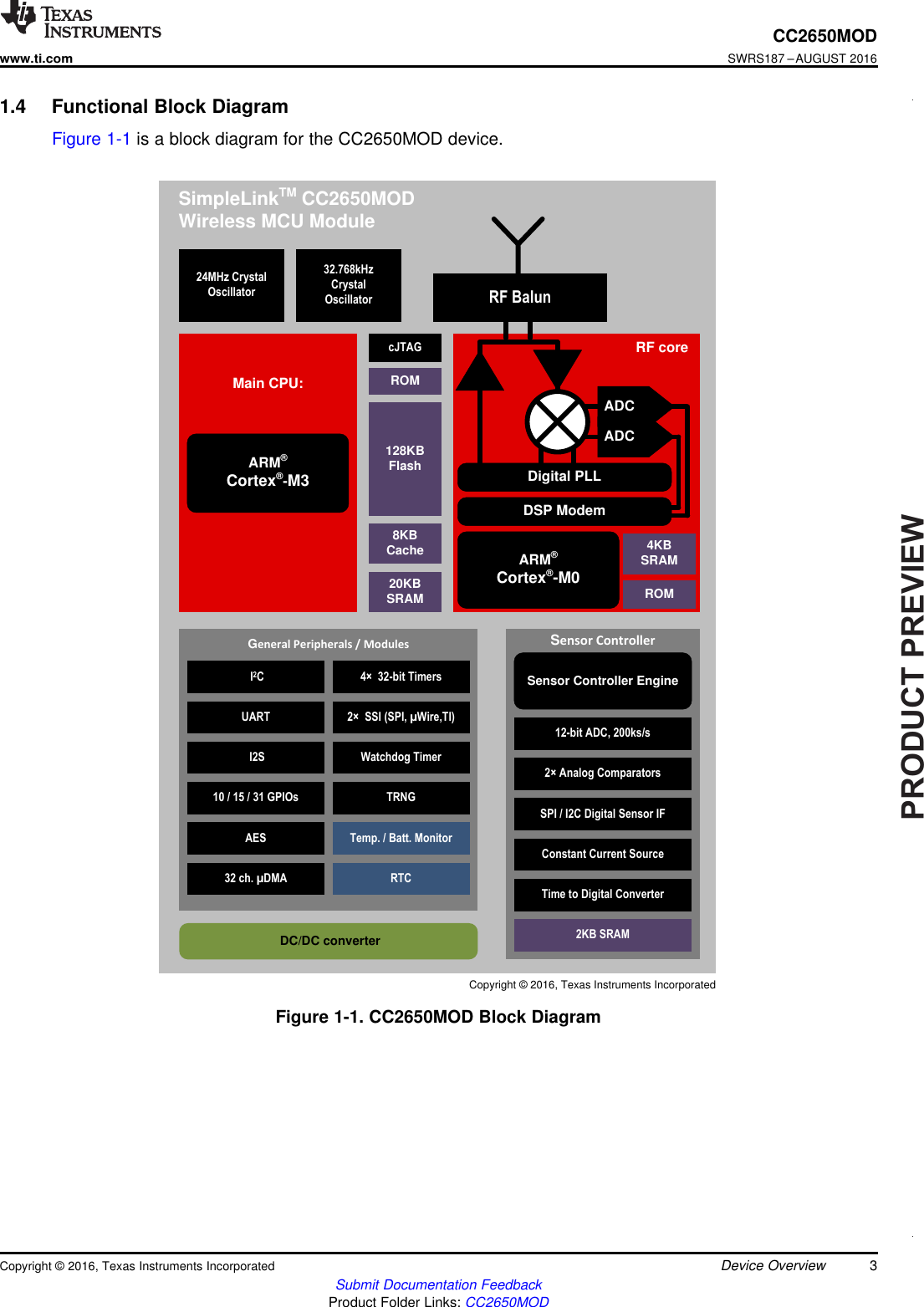
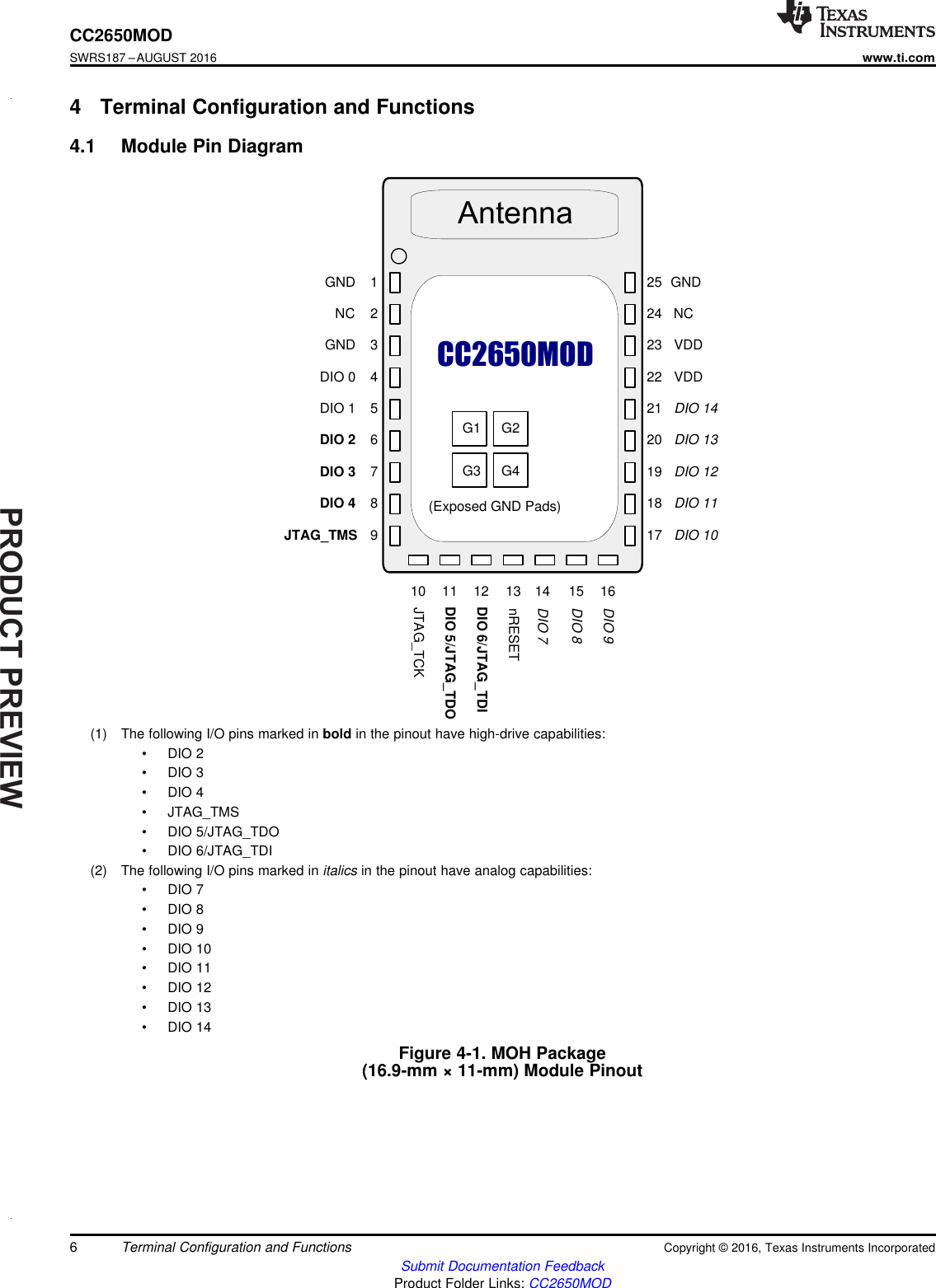
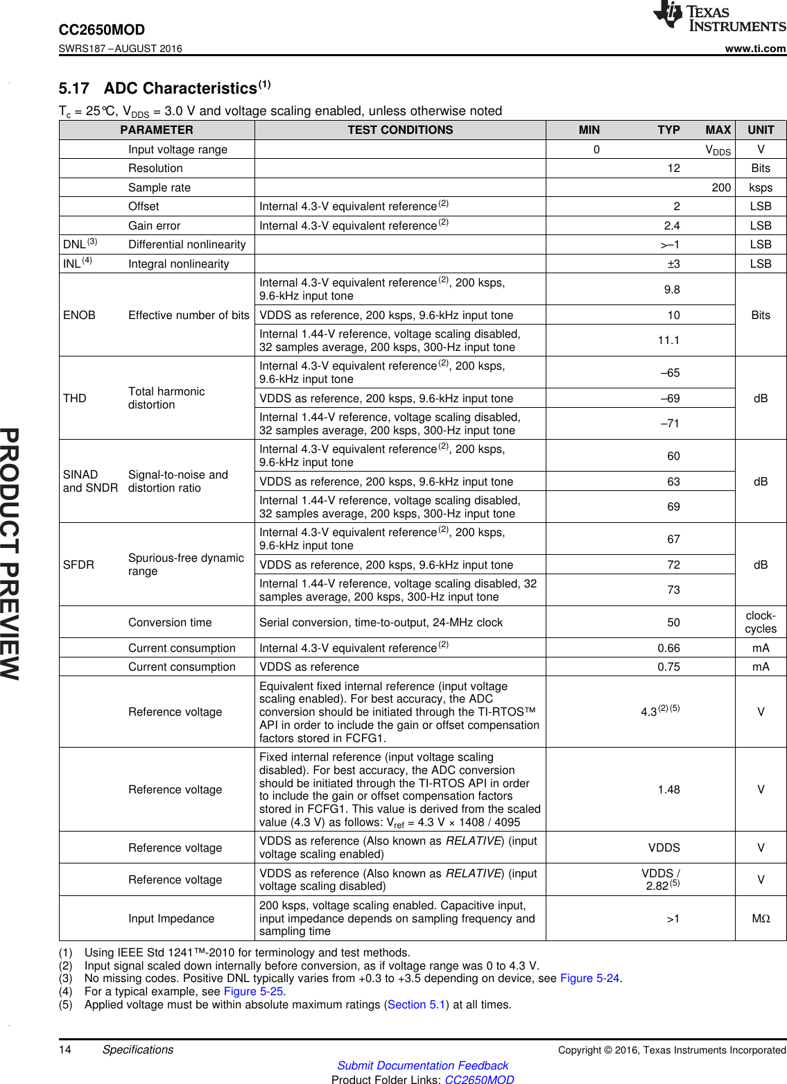
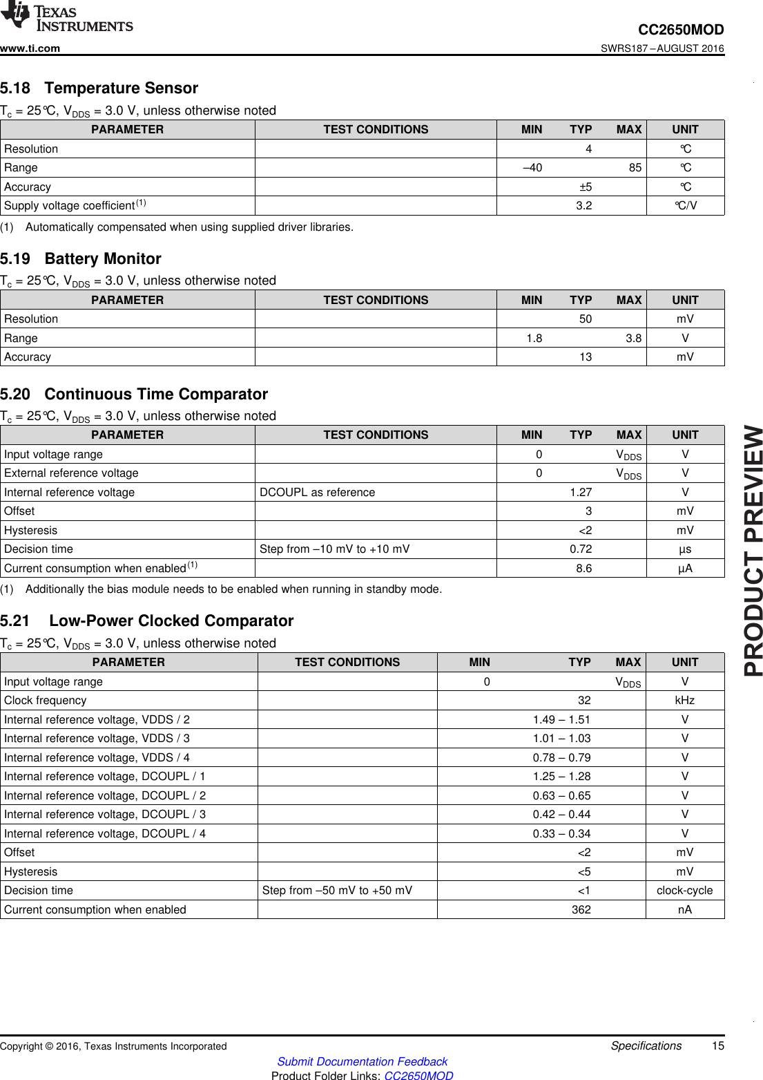
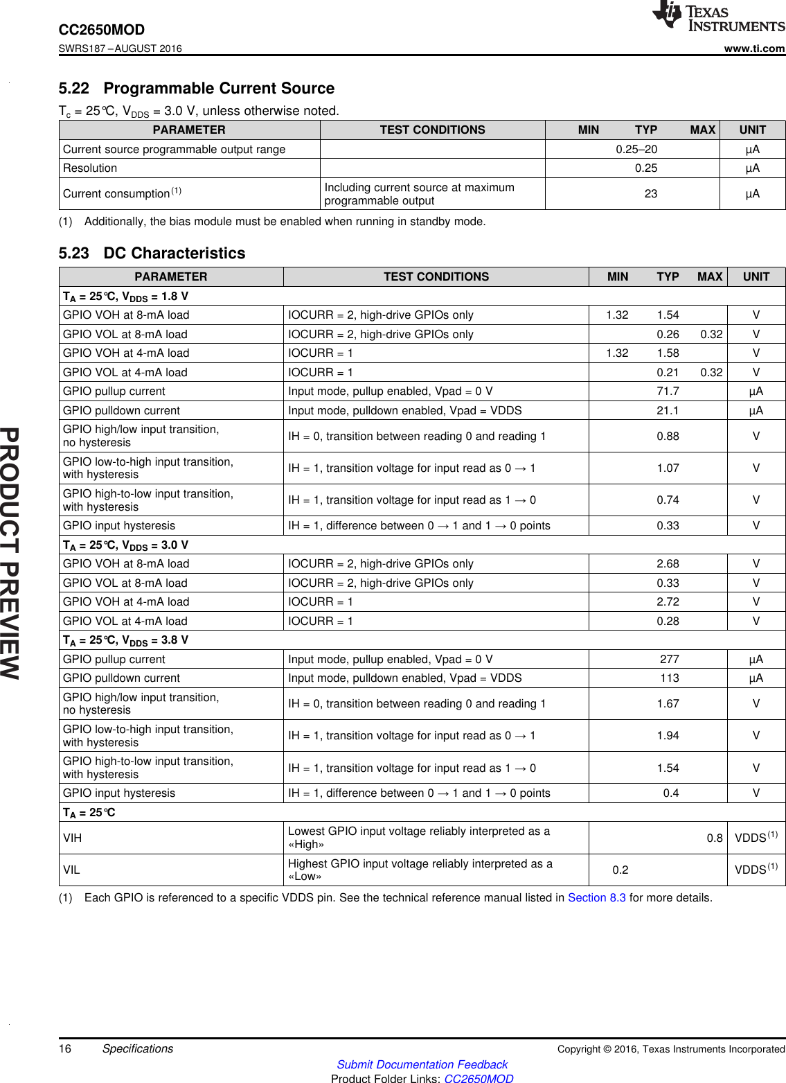
![PRODUCTPREVIEW17CC2650MODwww.ti.comSWRS187 –AUGUST 2016Submit Documentation FeedbackProduct Folder Links: CC2650MODSpecificationsCopyright © 2016, Texas Instruments Incorporated(1) °C/W = degrees Celsius per watt.(2) These values are based on a JEDEC-defined 2S2P system (with the exception of the Theta JC [RΘJC] value, which is based on aJEDEC-defined 1S0P system) and will change based on environment as well as application. For more information, see theseEIA/JEDEC standards:• JESD51-2, Integrated Circuits Thermal Test Method Environmental Conditions - Natural Convection (Still Air)• JESD51-3, Low Effective Thermal Conductivity Test Board for Leaded Surface Mount Packages• JESD51-7, High Effective Thermal Conductivity Test Board for Leaded Surface Mount Packages• JESD51-9, Test Boards for Area Array Surface Mount Package Thermal MeasurementsPower dissipation of 2 W and an ambient temperature of 70ºC is assumed.(3) m/s = meters per second.5.24 Thermal Resistance Characteristics for MOH PackageNAME DESCRIPTION °C/W(1) (2) AIR FLOW (m/s)(3)RΘJC Junction-to-case 20.0RΘJB Junction-to-board 15.3RΘJA Junction-to-free air 29.6 0RΘJMA Junction-to-moving air 25.0 1PsiJT Junction-to-package top 8.8 0PsiJB Junction-to-board 14.8 0(1) For smaller coin cell batteries, with high worst-case end-of-life equivalent source resistance, a 22-µF VDDS input capacitor (seeSection 7.1.1) must be used to ensure compliance with this slew rate.(2) Applications using RCOSC_LF as sleep timer must also consider the drift in frequency caused by a change in temperature (seeSection 5.16).(3) TA= –40°C to +85°C, VDDS = 1.7 V to 3.8 V, unless otherwise noted.(4) Tc= 25°C, VDDS = 3.0 V, unless otherwise noted. Device operating as SLAVE. For SSI MASTER operation, see Section 5.26.(5) Refer to SSI timing diagrams Figure 5-1,Figure 5-2, and Figure 5-3.5.25 Timing RequirementsMIN NOM MAX UNITRising supply-voltage slew rate 0 100 mV/µsFalling supply-voltage slew rate 0 20 mV/µsFalling supply-voltage slew rate, with low-power flash settings(1) 3 mV/µsPositive temperature gradient in standby(2) No limitation for negativetemperature gradient, oroutside standby mode 5 °C/sCONTROL INPUT AC CHARACTERISTICS(3)RESET_N low duration 1 µsSYNCHRONOUS SERIAL INTERFACE (SSI) (4)S1 (SLAVE) (5) tclk_per SSIClk period 12 65024 systemclocksS2 (5) tclk_high SSIClk high time 0.5 tclk_perS3(5) tclk_low SSIClk low time 0.5 tclk_per(1) Device operating as MASTER. For SSI SLAVE operation, see Section 5.25.(2) Refer to SSI timing diagrams Figure 5-1,Figure 5-2, and Figure 5-3.5.26 Switching CharacteristicsMeasured on the TI CC2650EM-5XD reference design with Tc= 25°C, VDDS = 3.0 V, unless otherwise noted.PARAMETER TEST CONDITIONS MIN TYP MAX UNITWAKEUP AND TIMINGIdle →Active 14 µsStandby →Active 151 µsShutdown →Active 1015 µsSYNCHRONOUS SERIAL INTERFACE (SSI) (1)S1 (TX only)(2) tclk_per (SSIClk period) One-way communication to SLAVE 4 65024 systemclocksS1 (TX and RX)(2) tclk_per (SSIClk period) Normal duplex operation 8 65024 systemclocks](https://usermanual.wiki/Texas-Instruments/26M1/User-Guide-3087552-Page-17.png)