Texas Instruments 26M1 BLE and 802.15.4 module User Manual
Texas Instruments Inc. BLE and 802.15.4 module Users Manual
Users Manual

PRODUCTPREVIEW
Product
Folder
Sample &
Buy
Technical
Documents
Tools &
Software
Support &
Community
An IMPORTANT NOTICE at the end of this data sheet addresses availability, warranty, changes, use in safety-critical applications,
intellectual property matters and other important disclaimers. PRODUCT PREVIEW Information. Product in design phase of
development. Subject to change or discontinuance without notice.
CC2650MOD
SWRS187 –AUGUST 2016
CC2650MOD SimpleLink™ Multistandard Wireless MCU Module
1 Device Overview
1
1.1 Features
1
• Microcontroller
– Powerful ARM®Cortex®-M3
– EEMBC CoreMark®Score: 142
– Up to 48-MHz Clock Speed
– 128KB of In-System Programmable Flash
– 8KB of SRAM for Cache
– 20KB of Ultra-Low Leakage SRAM
– 2-Pin cJTAG and JTAG Debugging
– Supports Over-The-Air Upgrade (OTA)
• Ultra-Low Power Sensor Controller
– Can Run Autonomous From the Rest of the
System
– 16-Bit Architecture
– 2KB of Ultra-Low Leakage SRAM for Code and
Data
• Efficient Code Size Architecture, Placing Drivers,
Bluetooth®low energy Controller, IEEE 802.15.4
MAC, and Bootloader in ROM
• Integrated Antenna
• Peripherals
– All Digital Peripheral Pins Can Be Routed to
Any GPIO
– Four General-Purpose Timer Modules (8 × 16-
Bit or 4 × 32-Bit Timer, PWM Each)
– 12-Bit ADC, 200-ksamples/s, 8-Channel Analog
MUX
– Continuous Time Comparator
– Ultra-Low Power Analog Comparator
– Programmable Current Source
– UART
– 2 × SSI (SPI, MICROWIRE, TI)
– I2C
– I2S
– Real-Time Clock (RTC)
– AES-128 Security Module
– True Random Number Generator (TRNG)
– 15 GPIOs
– Support for Eight Capacitive Sensing Buttons
– Integrated Temperature Sensor
• External System
– On-Chip internal DC-DC Converter
– No External Components Needed, Only Supply
Voltage
– Version With CC2592 Range Extender Available
• Low Power
– Wide Supply Voltage Range
• Operation from 1.8 to 3.8 V
– Active-Mode RX: 6.1 mA
– Active-Mode TX at 0 dBm: 6.1 mA
– Active-Mode TX at +5 dBm: 9.1 mA
– Active-Mode MCU: 61 µA/MHz
– Active-Mode MCU: 48.5 CoreMark/mA
– Active-Mode Sensor Controller: 8.2 µA/MHz
– Standby: 1 µA (RTC Running and RAM/CPU
Retention)
– Shutdown: 100 nA (Wake Up on External
Events)
• RF Section
– 2.4-GHz RF Transceiver Compatible With
Bluetooth low energy (BLE) 4.1 Specification
and IEEE 802.15.4 PHY and MAC
– Excellent Receiver Sensitivity (–97 dBm for
Bluetooth low energy and –100 dBm for
802.15.4), Selectivity, and Blocking
Performance
– Programmable Output Power up to +5 dBm
– Integrated Antenna
– Pre-Certified for Compliance With Worldwide
Radio Frequency Regulations
• ETSI (Europe)
• IC (Canada)
• FCC (USA)
• ARIB STD-T66 (Japan)
• Tools and Development Environment
– Full-Feature and Low-Cost Development Kits
– Multiple Reference Designs for Different RF
Configurations
– Packet Sniffer PC Software
– Sensor Controller Studio
– SmartRF™ Studio
– SmartRF Flash Programmer 2
– IAR Embedded Workbench®for ARM
– Code Composer Studio™

PRODUCTPREVIEW
2
CC2650MOD
SWRS187 –AUGUST 2016
www.ti.com
Submit Documentation Feedback
Product Folder Links: CC2650MOD
Device Overview Copyright © 2016, Texas Instruments Incorporated
1.2 Applications
• Consumer Electronics
• Mobile Phone Accessories
• Sports and Fitness Equipment
• HID Applications
• Home and Building Automation
• Lighting Control
• Alarm and Security
• Proximity Tags
• Medical
• Remote Controls
• Wireless Sensor Networks
(1) For more information, see Section 9,Mechanical Packaging and Orderable Information.
1.3 Description
The CC2650MOD device is a SimpleLink™ wireless MCU module that targets Bluetooth Smart, ZigBee®
and 6LoWPAN, and ZigBee®RF4CE remote control applications.
The module is based on the CC2650 Wireless MCU, a member of the CC26xx family of cost-effective,
ultra-low power, 2.4-GHz RF devices. Very low active RF and MCU current and low-power mode current
consumption provide excellent battery lifetime and allow for operation on small coin cell batteries and in
energy-harvesting applications.
The CC2650MOD contains a 32-bit ARM Cortex-M3 processor that runs at 48 MHz as the main processor
and a rich peripheral feature set that includes a unique ultra-low power sensor controller. This sensor
controller is ideal for interfacing external sensors or for collecting analog and digital data autonomously
while the rest of the system is in sleep mode. Thus, the CC2650MOD device is ideal for applications
within a whole range of products including industrial, consumer electronics, and medical devices.
The CC2650MOD is precertified for operation under the regulations of the FCC, IC, ETSI and ARIB.
These certifications save significant cost and effort for customers when integrating the module into their
products.
The Bluetooth low energy controller and the IEEE 802.15.4 MAC are embedded in the ROM and are partly
running on a separate ARM®Cortex®-M0 processor. This architecture improves overall system
performance and power consumption and makes more flash memory available.
The Bluetooth Smart and ZigBee stacks are available free of charge from www.ti.com.
Device Information(1)
PART NUMBER PACKAGE BODY SIZE
CC2650MODAMOH MOH (Module) 16.90 mm × 11.00 mm
PRODUCTPREVIEW
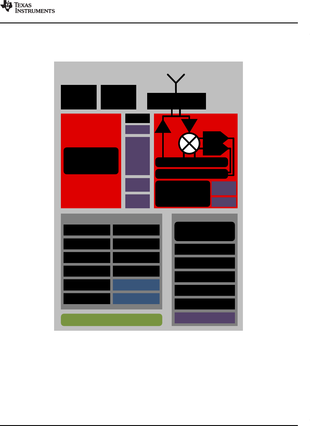
Main CPU:
128KB
Flash
Sensor Controller
cJTAG
20KB
SRAM
ROM
ARM®
Cortex®-M3
DC/DC converter
RF core
ARM®
Cortex®-M0
DSP Modem
4KB
SRAM
ROM
Sensor Controller Engine
2× Analog Comparators
12-bit ADC, 200ks/s
Constant Current Source
SPI / I2C Digital Sensor IF
2KB SRAM
Time to Digital Converter
General Peripherals / Modules
4× 32-bit Timers
2× SSI (SPI, µWire,TI)
Watchdog Timer
Temp. / Batt. Monitor
RTC
I2C
UART
I2S
10 / 15 / 31 GPIOs
AES
32 ch. µDMA
ADC
ADC
Digital PLL
SimpleLinkTM CC2650MOD
Wireless MCU Module
TRNG
8KB
Cache
24MHz Crystal
Oscillator
32.768kHz
Crystal
Oscillator RF Balun
Copyright © 2016, Texas Instruments Incorporated
3
CC2650MOD
www.ti.com
SWRS187 –AUGUST 2016
Submit Documentation Feedback
Product Folder Links: CC2650MOD
Device OverviewCopyright © 2016, Texas Instruments Incorporated
1.4 Functional Block Diagram
Figure 1-1 is a block diagram for the CC2650MOD device.
Figure 1-1. CC2650MOD Block Diagram

PRODUCTPREVIEW
4
CC2650MOD
SWRS187 –AUGUST 2016
www.ti.com
Submit Documentation Feedback
Product Folder Links: CC2650MOD
Revision History Copyright © 2016, Texas Instruments Incorporated
Table of Contents
1 Device Overview ......................................... 1
1.1 Features .............................................. 1
1.2 Applications........................................... 2
1.3 Description............................................ 2
1.4 Functional Block Diagram ............................ 3
2 Revision History ......................................... 4
3 Device Comparison ..................................... 5
4 Terminal Configuration and Functions.............. 6
4.1 Module Pin Diagram.................................. 6
4.2 Pin Functions ......................................... 7
5 Specifications ............................................ 8
5.1 Absolute Maximum Ratings .......................... 8
5.2 ESD Ratings.......................................... 8
5.3 Recommended Operating Conditions ................ 8
5.4 Power Consumption Summary ....................... 9
5.5 General Characteristics .............................. 9
5.6 Antenna ............................................. 10
5.7 1-Mbps GFSK (Bluetooth low energy) – RX ........ 10
5.8 1-Mbps GFSK (Bluetooth low energy) – TX ........ 11
5.9 2-Mbps GFSK (Bluetooth low energy) – RX ........ 11
5.10 2-Mbps GFSK (Bluetooth low energy) – TX ........ 12
5.11 IEEE 802.15.4 (Offset Q-PSK DSSS, 250 kbps) –
RX ................................................... 12
5.12 IEEE 802.15.4 (Offset Q-PSK DSSS, 250 kbps) –
TX ................................................... 13
5.13 24-MHz Crystal Oscillator (XOSC_HF) ............. 13
5.14 32.768-kHz Crystal Oscillator (XOSC_LF).......... 13
5.15 48-MHz RC Oscillator (RCOSC_HF) ............... 13
5.16 32-kHz RC Oscillator (RCOSC_LF)................. 13
5.17 ADC Characteristics................................. 14
5.18 Temperature Sensor ................................ 15
5.19 Battery Monitor...................................... 15
5.20 Continuous Time Comparator....................... 15
5.21 Low-Power Clocked Comparator ................... 15
5.22 Programmable Current Source ..................... 16
5.23 DC Characteristics .................................. 16
5.24 Thermal Resistance Characteristics for MOH
Package ............................................. 17
5.25 Timing Requirements ............................... 17
5.26 Switching Characteristics ........................... 17
5.27 Typical Characteristics .............................. 20
6 Detailed Description ................................... 25
6.1 Overview ............................................ 25
6.2 Functional Block Diagram........................... 25
6.3 Main CPU ........................................... 26
6.4 RF Core ............................................. 26
6.5 Sensor Controller ................................... 27
6.6 Memory.............................................. 28
6.7 Debug ............................................... 28
6.8 Power Management................................. 29
6.9 Clock Systems ...................................... 30
6.10 General Peripherals and Modules .................. 30
6.11 System Architecture................................. 32
6.12 Certification.......................................... 32
6.13 End Product Labeling ............................... 33
6.14 Manual Information to the End User ................ 33
7 Application, Implementation, and Layout ......... 34
7.1 Application Information .............................. 34
8 Device and Documentation Support ............... 35
8.1 Device Nomenclature ............................... 35
8.2 Tools and Software ................................. 36
8.3 Documentation Support ............................. 37
8.4 Texas Instruments Low-Power RF Website ........ 37
8.5 Low-Power RF eNewsletter ......................... 37
8.6 Community Resources.............................. 38
8.7 Additional Information ............................... 38
8.8 Trademarks.......................................... 38
8.9 Electrostatic Discharge Caution..................... 39
8.10 Export Control Notice ............................... 39
8.11 Glossary ............................................. 39
9 Mechanical Packaging and Orderable
Information .............................................. 39
9.1 Packaging Information .............................. 39
2 Revision History
DATE REVISION NOTES
August 2016 * Initial Release

PRODUCTPREVIEW
5
CC2650MOD
www.ti.com
SWRS187 –AUGUST 2016
Submit Documentation Feedback
Product Folder Links: CC2650MOD
Device ComparisonCopyright © 2016, Texas Instruments Incorporated
3 Device Comparison
Table 3-1. Device Family Overview
DEVICE PHY SUPPORT FLASH
(KB) RAM (KB) GPIO PACKAGE
CC2650MODAMOH Multiprotocol 128 20 15 MOH
PRODUCTPREVIEW
CC2650MOD
(Exposed GND Pads)
3
1
2
4
5
6
7 19
21
20
18
17
23
22
10 11 12 13 14 15 16
Antenna
GND
DIO 0
DIO 1
DIO 2
DIO 3
DIO 4
JTAG_TMS
VDD
VDD
DIO 14
DIO 13
DIO 12
DIO 11
DIO 10
JTAG_TCK
DIO 5/JTAG_TDO
DIO 6/JTAG_TDI
nRESET
DIO 7
DIO 8
DIO 9
8
9
25
24
GND GND
G1 G2
G3 G4
NC NC
6
CC2650MOD
SWRS187 –AUGUST 2016
www.ti.com
Submit Documentation Feedback
Product Folder Links: CC2650MOD
Terminal Configuration and Functions Copyright © 2016, Texas Instruments Incorporated
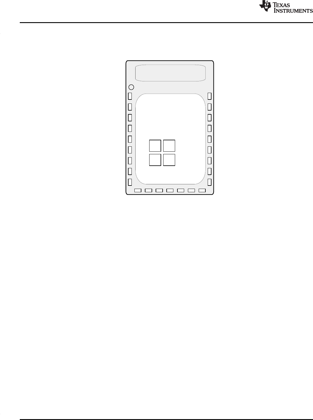
4 Terminal Configuration and Functions
4.1 Module Pin Diagram
(1) The following I/O pins marked in bold in the pinout have high-drive capabilities:
• DIO 2
• DIO 3
• DIO 4
• JTAG_TMS
• DIO 5/JTAG_TDO
• DIO 6/JTAG_TDI
(2) The following I/O pins marked in italics in the pinout have analog capabilities:
• DIO 7
• DIO 8
• DIO 9
• DIO 10
• DIO 11
• DIO 12
• DIO 13
• DIO 14
Figure 4-1. MOH Package
(16.9-mm × 11-mm) Module Pinout

PRODUCTPREVIEW
7
CC2650MOD
www.ti.com
SWRS187 –AUGUST 2016
Submit Documentation Feedback
Product Folder Links: CC2650MOD
Terminal Configuration and FunctionsCopyright © 2016, Texas Instruments Incorporated
4.2 Pin Functions
Table 4-1. Signal Descriptions – MOH Package
PIN NAME PIN NO. PIN TYPE DESCRIPTION
DIO_0 4 Digital I/O GPIO, Sensor Controller
DIO_1 5 Digital I/O GPIO, Sensor Controller
DIO_2 6 Digital I/O GPIO, Sensor Controller, high-drive capability
DIO_3 7 Digital I/O GPIO, Sensor Controller, high-drive capability
DIO_4 8 Digital I/O GPIO, Sensor Controller, high-drive capability
DIO_5/JTAG_TDO 11 Digital I/O GPIO, high-drive capability, JTAG_TDO
DIO_6/JTAG_TDI 12 Digital I/O GPIO, high-drive capability, JTAG_TDI
DIO_7 14 Digital I/O, Analog I/O GPIO, Sensor Controller, analog
DIO_8 15 Digital I/O, Analog I/O GPIO, Sensor Controller, analog
DIO_9 16 Digital I/O, Analog I/O GPIO, Sensor Controller, analog
DIO_10 17 Digital I/O, Analog I/O GPIO, Sensor Controller, analog
DIO_11 18 Digital I/O, Analog I/O GPIO, Sensor Controller, analog
DIO_12 19 Digital I/O, Analog I/O GPIO, Sensor Controller, analog
DIO_13 20 Digital I/O, Analog I/O GPIO, Sensor Controller, analog
DIO_14 21 Digital I/O, Analog I/O GPIO, Sensor Controller, analog
EGP G1, G2, G3, G4 Power Ground – Exposed ground pad
GND 1, 25 — Ground
JTAG_TCKC 10 Digital I/O JTAG TCKC
JTAG_TMSC 9 Digital I/O JTAG TMSC, high-drive capability
NC 2, 24 NC Not Connected—TI recommends that these pins are left
floating
RESET_N 13 Digital input Reset, active low. No internal pullup
VDDS 22, 23 Power 1.8-V to 3.8-V main chip supply
PRODUCTPREVIEW
8
CC2650MOD
SWRS187 –AUGUST 2016
www.ti.com
Submit Documentation Feedback
Product Folder Links: CC2650MOD
Specifications Copyright © 2016, Texas Instruments Incorporated
(1) Stresses beyond those listed under Absolute Maximum Ratings may cause permanent damage to the device. These are stress ratings
only, and functional operation of the device at these or any other conditions beyond those indicated under Recommended Operating
Conditions is not implied. Exposure to absolute-maximum-rated conditions for extended periods may affect device reliability.
(2) All voltage values are with respect to ground, unless otherwise noted.
(3) Including analog capable DIO.
5 Specifications
5.1 Absolute Maximum Ratings
over operating free-air temperature range (unless otherwise noted)(1)(2)
MIN MAX UNIT
VDDS Supply voltage –0.3 4.1 V
Voltage on any digital pin(3) –0.3 VDDS + 0.3, max 4.1 V
Vin Voltage on ADC input
Voltage scaling enabled –0.3 VDDS
VVoltage scaling disabled, internal reference –0.3 1.49
Voltage scaling disabled, VDDS as reference –0.3 VDDS / 2.9
Input RF level 5 dBm
Tstg Storage temperature –40 85 °C
(1) JEDEC document JEP155 states that 500-V HBM allows safe manufacturing with a standard ESD control process.
(2) JEDEC document JEP157 states that 250-V CDM allows safe manufacturing with a standard ESD control process.
5.2 ESD Ratings
VALUE UNIT
VESD Electrostatic discharge
Human body model (HBM), per ANSI/ESDA/JEDEC
JS001(1) All pins ±2500
V
Charged device model (CDM), per JESD22-C101(2) RF pins ±750
Non-RF pins ±750
5.3 Recommended Operating Conditions
MIN MAX UNIT
Ambient temperature –40 85 °C
Operating supply voltage (VDDS)
For operation in battery-powered and 3.3-V
systems
(internal DC-DC can be used to minimize power
consumption)
1.8 3.8 V
PRODUCTPREVIEW
9
CC2650MOD
www.ti.com
SWRS187 –AUGUST 2016
Submit Documentation Feedback
Product Folder Links: CC2650MOD
SpecificationsCopyright © 2016, Texas Instruments Incorporated
(1) Iperi is not supported in Standby or Shutdown.
5.4 Power Consumption Summary
Tc= 25°C, VDDS = 3.0 V with internal DC-DC converter, unless otherwise noted
PARAMETER TEST CONDITIONS MIN TYP MAX UNIT
Icore Core current consumption
Reset. RESET_N pin asserted or VDDS below
Power-on-Reset threshold 100 nA
Shutdown. No clocks running, no retention 150
Standby. With RTC, CPU, RAM and (partial)
register retention. RCOSC_LF 1
µA
Standby. With RTC, CPU, RAM and (partial)
register retention. XOSC_LF 1.2
Standby. With Cache, RTC, CPU, RAM and
(partial) register retention. RCOSC_LF 2.5
Standby. With Cache, RTC, CPU, RAM and
(partial) register retention. XOSC_LF 2.7
Idle. Supply systems and RAM powered. 550
Active. Core running CoreMark 1.45 mA +
31 µA/MHz
Radio RX 6.1
mARadio TX, 0-dBm output power 6.1
Radio TX, 5-dBm output power 9.1
Peripheral Current Consumption (Adds to core current Icore for each peripheral unit activated)(1)
Iperi
Peripheral power domain Delta current with domain enabled 20 µA
Serial power domain Delta current with domain enabled 13 µA
RF Core Delta current with power domain enabled, clock
enabled, RF Core Idle 237 µA
µDMA Delta current with clock enabled, module idle 130 µA
Timers Delta current with clock enabled, module idle 113 µA
I2C Delta current with clock enabled, module idle 12 µA
I2S Delta current with clock enabled, module idle 36 µA
SSI Delta current with clock enabled, module idle 93 µA
UART Delta current with clock enabled, module idle 164 µA
(1) This number is dependent on Flash aging and will increase over time and erase cycles
5.5 General Characteristics
Tc= 25°C, VDDS = 3.0 V, unless otherwise noted
PARAMETER TEST CONDITIONS MIN TYP MAX UNIT
FLASH MEMORY
Supported flash erase cycles before
failure 100 k Cycles
Flash page/sector erase current Average delta current 12.6 mA
Flash page/sector erase time(1) 8 ms
Flash page/sector size 4 KB
Flash write current Average delta current, 4 bytes at a time 8.15 mA
Flash write time(1) 4 bytes at a time 8 µs

PRODUCTPREVIEW
10
CC2650MOD
SWRS187 –AUGUST 2016
www.ti.com
Submit Documentation Feedback
Product Folder Links: CC2650MOD
Specifications Copyright © 2016, Texas Instruments Incorporated
5.6 Antenna
Tc= 25°C, VDDS = 3.0 V, unless otherwise noted.
PARAMETER TEST CONDITIONS MIN TYP MAX UNIT
Polarization Linear
Peak Gain 2450 MHz 1.26 dBi
Efficiency 2450 MHz 56.9 %
(1) Numbers given as I/C dB
(2) X / Y, where X is +N MHz and Y is –N MHz
(3) Excluding one exception at Fwanted / 2, per Bluetooth Specification
5.7 1-Mbps GFSK (Bluetooth low energy) – RX
RF performance is specified in a single ended 50-Ωreference plane at the antenna feeding point with Tc= 25°C,
VDDS = 3.0 V, fRF = 2440 MHz, unless otherwise noted.
PARAMETER TEST CONDITIONS MIN TYP MAX UNIT
Receiver sensitivity BER = 10–3 –97 dBm
Receiver saturation BER = 10–3 4 dBm
Frequency error tolerance Difference between center frequency of the received RF signal
and local oscillator frequency. –350 350 kHz
Data rate error tolerance –750 750 ppm
Co-channel rejection(1) Wanted signal at –67 dBm, modulated interferer in channel,
BER = 10–3 –6 dB
Selectivity, ±1 MHz(1) Wanted signal at –67 dBm, modulated interferer at ±1 MHz,
BER = 10–3 7 / 3(2) dB
Selectivity, ±2 MHz(1) Wanted signal at –67 dBm, modulated interferer at ±2 MHz,
BER = 10–3 34 / 25(2) dB
Selectivity, ±3 MHz(1) Wanted signal at –67 dBm, modulated interferer at ±3 MHz,
BER = 10–3 38 / 26(2) dB
Selectivity, ±4 MHz(1) Wanted signal at –67 dBm, modulated interferer at ±4 MHz,
BER = 10–3 42 / 29(2) dB
Selectivity, ±5 MHz or more(1) Wanted signal at –67 dBm, modulated interferer at ≥±5 MHz,
BER = 10–3 32 dB
Selectivity, Image frequency(1) Wanted signal at –67 dBm, modulated interferer at image
frequency, BER = 10–3 25 dB
Selectivity,
Image frequency ±1 MHz(1) Wanted signal at –67 dBm, modulated interferer at ±1 MHz from
image frequency, BER = 10–3 3 / 26(2) dB
Out-of-band blocking(3) 30 MHz to 2000 MHz –20 dBm
Out-of-band blocking 2003 MHz to 2399 MHz –5 dBm
Out-of-band blocking 2484 MHz to 2997 MHz –8 dBm
Out-of-band blocking 3000 MHz to 12.75 GHz –8 dBm
Intermodulation Wanted signal at 2402 MHz, –64 dBm. Two interferers at 2405
and 2408 MHz respectively, at the given power level –34 dBm
Spurious emissions,
30 MHz to 1000 MHz
Conducted measurement in a 50-Ωsingle-ended load. Suitable
for systems targeting compliance with EN 300 328, EN 300 440
class 2, FCC CFR47, Part 15 and ARIB STD-T-66 –71 dBm
Spurious emissions,
1 GHz to 12.75 GHz
Conducted measurement in a 50-Ωsingle-ended load. Suitable
for systems targeting compliance with EN 300 328, EN 300 440
class 2, FCC CFR47, Part 15 and ARIB STD-T-66 –62 dBm
RSSI dynamic range 70 dB
RSSI accuracy ±4 dB

PRODUCTPREVIEW
11
CC2650MOD
www.ti.com
SWRS187 –AUGUST 2016
Submit Documentation Feedback
Product Folder Links: CC2650MOD
SpecificationsCopyright © 2016, Texas Instruments Incorporated
(1) Suitable for systems targeting compliance with worldwide radio-frequency regulations ETSI EN 300 328 and EN 300 440 Class 2
(Europe), FCC CFR47 Part 15 (US), and ARIB STD-T66 (Japan)
5.8 1-Mbps GFSK (Bluetooth low energy) – TX
RF performance is specified in a single ended 50-Ωreference plane at the antenna feeding point with Tc= 25°C,
VDDS = 3.0 V, fRF = 2440 MHz, unless otherwise noted.
PARAMETER TEST CONDITIONS MIN TYP MAX UNIT
Output power, highest setting 5 dBm
Output power, lowest setting –21 dBm
Spurious emission conducted
measurement(1)
f < 1 GHz, outside restricted bands –43 dBm
f < 1 GHz, restricted bands ETSI –65 dBm
f < 1 GHz, restricted bands FCC –76 dBm
f > 1 GHz, including harmonics –46 dBm
(1) Numbers given as I/C dB.
(2) X / Y, where X is +N MHz and Y is –N MHz.
(3) Excluding one exception at Fwanted / 2, per Bluetooth Specification.
5.9 2-Mbps GFSK (Bluetooth low energy) – RX
RF performance is specified in a single ended 50-Ωreference plane at the antenna feeding point with Tc= 25°C,
VDDS = 3.0 V, fRF = 2440 MHz, unless otherwise noted.
PARAMETER TEST CONDITIONS MIN TYP MAX UNIT
Receiver sensitivity Differential mode. Measured at the CC2650EM-5XD
SMA connector, BER = 10–3 –91.7 dBm
Receiver saturation Differential mode. Measured at the CC2650EM-5XD
SMA connector, BER = 10–3 4 dBm
Frequency error tolerance Difference between the incoming carrier frequency
and the internally generated carrier frequency –300 500 kHz
Data rate error tolerance Difference between incoming data rate and the
internally generated data rate –1000 1000 ppm
Co-channel rejection (1) Wanted signal at –67 dBm, modulated interferer in
channel,
BER = 10–3 –7 dB
Selectivity, ±2 MHz (1)
Wanted signal at –67 dBm, modulated interferer at
±2 MHz,
Image frequency is at –2 MHz
BER = 10–3
8 / 4(2) dB
Selectivity, ±4 MHz (1) Wanted signal at –67 dBm, modulated interferer at
±4 MHz,
BER = 10–3 31 / 26(2) dB
Selectivity, ±6 MHz (1) Wanted signal at –67 dBm, modulated interferer at
±6 MHz,
BER = 10–3 37 / 38(2) dB
Alternate channel rejection, ±7
MHz(1) Wanted signal at –67 dBm, modulated interferer at ≥
±7 MHz, BER = 10–3 37 / 36(2) dB
Selectivity, Image frequency(1) Wanted signal at –67 dBm, modulated interferer at
image frequency,
BER = 10–3 4 dB
Selectivity, Image frequency
±2 MHz(1)
Note that Image frequency + 2 MHz is the Co-
channel. Wanted signal at –67 dBm, modulated
interferer at ±2 MHz from image frequency,
BER = 10–3
–7 / 26(2) dB
Out-of-band blocking (3) 30 MHz to 2000 MHz –33 dBm
Out-of-band blocking 2003 MHz to 2399 MHz –15 dBm
Out-of-band blocking 2484 MHz to 2997 MHz –12 dBm
Out-of-band blocking 3000 MHz to 12.75 GHz –10 dBm
Intermodulation Wanted signal at 2402 MHz, –64 dBm. Two
interferers at 2405 and 2408 MHz respectively, at
the given power level –45 dBm

PRODUCTPREVIEW
12
CC2650MOD
SWRS187 –AUGUST 2016
www.ti.com
Submit Documentation Feedback
Product Folder Links: CC2650MOD
Specifications Copyright © 2016, Texas Instruments Incorporated
(1) Suitable for systems targeting compliance with worldwide radio-frequency regulations ETSI EN 300 328 and EN 300 440 Class 2
(Europe), FCC CFR47 Part 15 (US), and ARIB STD-T66 (Japan).
5.10 2-Mbps GFSK (Bluetooth low energy) – TX
RF performance is specified in a single ended 50-Ωreference plane at the antenna feeding point with Tc= 25°C,
VDDS = 3.0 V, fRF = 2440 MHz, unless otherwise noted.
PARAMETER TEST CONDITIONS MIN TYP MAX UNIT
Output power, highest setting Differential mode, delivered to a single-ended 50-Ωload
through a balun 5 dBm
Output power, highest setting Measured on CC2650EM-4XS, delivered to a single-ended
50-Ωload 2 dBm
Output power, lowest setting Delivered to a single-ended 50-Ωload through a balun –21 dBm
Spurious emission conducted
measurement(1)
f < 1 GHz, outside restricted bands –43 dBm
f < 1 GHz, restricted bands ETSI –65 dBm
f < 1 GHz, restricted bands FCC –76 dBm
f > 1 GHz, including harmonics –46 dBm
5.11 IEEE 802.15.4 (Offset Q-PSK DSSS, 250 kbps) – RX
RF performance is specified in a single ended 50-Ωreference plane at the antenna feeding point with Tc= 25°C,
VDDS = 3.0 V, unless otherwise noted.
PARAMETER TEST CONDITIONS MIN TYP MAX UNIT
Receiver sensitivity PER = 1% –100 dBm
Receiver saturation PER = 1% +4 dBm
Adjacent channel rejection Wanted signal at –82 dBm, modulated interferer at ±5 MHz,
PER = 1% 39 dB
Alternate channel rejection Wanted signal at –82 dBm, modulated interferer at ±10 MHz,
PER = 1% 52 dB
Channel rejection, ±15 MHz or
more
Wanted signal at –82 dBm, undesired signal is IEEE 802.15.4
modulated channel, stepped through all channels 2405 to
2480 MHz, PER = 1% 57 dB
Blocking and desensitization,
5 MHz from upper band edge Wanted signal at –97 dBm (3 dB above the sensitivity level),
CW jammer, PER = 1% 64 dB
Blocking and desensitization,
10 MHz from upper band edge Wanted signal at –97 dBm (3 dB above the sensitivity level),
CW jammer, PER = 1% 64 dB
Blocking and desensitization,
20 MHz from upper band edge Wanted signal at –97 dBm (3 dB above the sensitivity level),
CW jammer, PER = 1% 65 dB
Blocking and desensitization,
50 MHz from upper band edge Wanted signal at –97 dBm (3 dB above the sensitivity level),
CW jammer, PER = 1% 68 dB
Blocking and desensitization,
–5 MHz from lower band edge Wanted signal at –97 dBm (3 dB above the sensitivity level),
CW jammer, PER = 1% 63 dB
Blocking and desensitization,
–10 MHz from lower band edge Wanted signal at –97 dBm (3 dB above the sensitivity level),
CW jammer, PER = 1% 63 dB
Blocking and desensitization,
–20 MHz from lower band edge Wanted signal at –97 dBm (3 dB above the sensitivity level),
CW jammer, PER = 1% 65 dB
Blocking and desensitization,
–50 MHz from lower band edge Wanted signal at –97 dBm (3 dB above the sensitivity level),
CW jammer, PER = 1% 67 dB
Spurious emissions,
30 MHz to 1000 MHz
Conducted measurement in a 50-Ωsingle-ended load.
Suitable for systems targeting compliance with EN 300 328,
EN 300 440 class 2, FCC CFR47, Part 15 and ARIB STD-T-
66
–71 dBm
Spurious emissions,
1 GHz to 12.75 GHz
Conducted measurement in a 50-Ωsingle-ended load.
Suitable for systems targeting compliance with EN 300 328,
EN 300 440 class 2, FCC CFR47, Part 15 and ARIB STD-T-
66
–62 dBm
Frequency error tolerance Difference between center frequency of the received RF
signal and local oscillator frequency >200 ppm
RSSI dynamic range 100 dB
RSSI accuracy ±4 dB
PRODUCTPREVIEW
13
CC2650MOD
www.ti.com
SWRS187 –AUGUST 2016
Submit Documentation Feedback
Product Folder Links: CC2650MOD
SpecificationsCopyright © 2016, Texas Instruments Incorporated
(1) Suitable for systems targeting compliance with worldwide radio-frequency regulations ETSI EN 300 328 and EN 300 440 Class 2
(Europe), FCC CFR47 Part 15 (US), and ARIB STD-T66 (Japan)
5.12 IEEE 802.15.4 (Offset Q-PSK DSSS, 250 kbps) – TX
RF performance is specified in a single ended 50-Ωreference plane at the antenna feeding point with Tc= 25°C,
VDDS = 3.0 V, unless otherwise noted.
PARAMETER TEST CONDITIONS MIN TYP MAX UNIT
Output power, highest setting 5 dBm
Output power, lowest setting –21 dBm
Error vector magnitude At maximum output power 2%
Spurious emission conducted
measurement(1)
f < 1 GHz, outside restricted bands –43
dBm
f < 1 GHz, restricted bands ETSI –65
f < 1 GHz, restricted bands FCC –76
f > 1 GHz, including harmonics –46
(1) Probing or otherwise stopping the XTAL while the DC-DC converter is enabled may cause permanent damage to the device.
(2) Includes initial tolerance of the crystal, drift over temperature, aging and frequency pulling due to incorrect load capacitance. As per
Bluetooth and IEEE 802.15.4 specification
(3) Kick-started based on a temperature and aging compensated RCOSC_HF using precharge injection
5.13 24-MHz Crystal Oscillator (XOSC_HF)(1)
Tc= 25°C, VDDS = 3.0 V, unless otherwise noted
PARAMETER TEST CONDITIONS MIN TYP MAX UNIT
Crystal frequency 24 MHz
Crystal frequency tolerance(2) –40 40 ppm
Start-up time(3) 150 µs
5.14 32.768-kHz Crystal Oscillator (XOSC_LF)
Tc= 25°C, VDDS = 3.0 V, unless otherwise noted
PARAMETER TEST CONDITIONS MIN TYP MAX UNIT
Crystal frequency 32.768 kHz
Crystal frequency tolerance, Bluetooth low
energy applications –250 250 ppm
(1) Accuracy relatively to the calibration source (XOSC_HF).
5.15 48-MHz RC Oscillator (RCOSC_HF)
Tc= 25°C, VDDS = 3.0 V, unless otherwise noted
PARAMETER TEST CONDITIONS MIN TYP MAX UNIT
Frequency 48 MHz
Uncalibrated frequency accuracy ±1%
Calibrated frequency accuracy(1) ±0.25%
Start-up time 5 µs
5.16 32-kHz RC Oscillator (RCOSC_LF)
Tc= 25°C, VDDS = 3.0 V, unless otherwise noted
PARAMETER TEST CONDITIONS MIN TYP MAX UNIT
Calibrated frequency 32.8 kHz
Temperature coefficient 50 ppm/°C

PRODUCTPREVIEW
14
CC2650MOD
SWRS187 –AUGUST 2016
www.ti.com
Submit Documentation Feedback
Product Folder Links: CC2650MOD
Specifications Copyright © 2016, Texas Instruments Incorporated
(1) Using IEEE Std 1241™-2010 for terminology and test methods.
(2) Input signal scaled down internally before conversion, as if voltage range was 0 to 4.3 V.
(3) No missing codes. Positive DNL typically varies from +0.3 to +3.5 depending on device, see Figure 5-24.
(4) For a typical example, see Figure 5-25.
(5) Applied voltage must be within absolute maximum ratings (Section 5.1) at all times.
5.17 ADC Characteristics(1)
Tc= 25°C, VDDS = 3.0 V and voltage scaling enabled, unless otherwise noted
PARAMETER TEST CONDITIONS MIN TYP MAX UNIT
Input voltage range 0 VDDS V
Resolution 12 Bits
Sample rate 200 ksps
Offset Internal 4.3-V equivalent reference(2) 2 LSB
Gain error Internal 4.3-V equivalent reference(2) 2.4 LSB
DNL(3) Differential nonlinearity >–1 LSB
INL(4) Integral nonlinearity ±3 LSB
ENOB Effective number of bits
Internal 4.3-V equivalent reference(2), 200 ksps,
9.6-kHz input tone 9.8
BitsVDDS as reference, 200 ksps, 9.6-kHz input tone 10
Internal 1.44-V reference, voltage scaling disabled,
32 samples average, 200 ksps, 300-Hz input tone 11.1
THD Total harmonic
distortion
Internal 4.3-V equivalent reference(2), 200 ksps,
9.6-kHz input tone –65
dBVDDS as reference, 200 ksps, 9.6-kHz input tone –69
Internal 1.44-V reference, voltage scaling disabled,
32 samples average, 200 ksps, 300-Hz input tone –71
SINAD
and SNDR Signal-to-noise and
distortion ratio
Internal 4.3-V equivalent reference(2), 200 ksps,
9.6-kHz input tone 60
dBVDDS as reference, 200 ksps, 9.6-kHz input tone 63
Internal 1.44-V reference, voltage scaling disabled,
32 samples average, 200 ksps, 300-Hz input tone 69
SFDR Spurious-free dynamic
range
Internal 4.3-V equivalent reference(2), 200 ksps,
9.6-kHz input tone 67
dBVDDS as reference, 200 ksps, 9.6-kHz input tone 72
Internal 1.44-V reference, voltage scaling disabled, 32
samples average, 200 ksps, 300-Hz input tone 73
Conversion time Serial conversion, time-to-output, 24-MHz clock 50 clock-
cycles
Current consumption Internal 4.3-V equivalent reference(2) 0.66 mA
Current consumption VDDS as reference 0.75 mA
Reference voltage
Equivalent fixed internal reference (input voltage
scaling enabled). For best accuracy, the ADC
conversion should be initiated through the TI-RTOS™
API in order to include the gain or offset compensation
factors stored in FCFG1.
4.3(2)(5) V
Reference voltage
Fixed internal reference (input voltage scaling
disabled). For best accuracy, the ADC conversion
should be initiated through the TI-RTOS API in order
to include the gain or offset compensation factors
stored in FCFG1. This value is derived from the scaled
value (4.3 V) as follows: Vref = 4.3 V × 1408 / 4095
1.48 V
Reference voltage VDDS as reference (Also known as RELATIVE) (input
voltage scaling enabled) VDDS V
Reference voltage VDDS as reference (Also known as RELATIVE) (input
voltage scaling disabled) VDDS /
2.82(5) V
Input Impedance 200 ksps, voltage scaling enabled. Capacitive input,
input impedance depends on sampling frequency and
sampling time >1 MΩ
PRODUCTPREVIEW
15
CC2650MOD
www.ti.com
SWRS187 –AUGUST 2016
Submit Documentation Feedback
Product Folder Links: CC2650MOD
SpecificationsCopyright © 2016, Texas Instruments Incorporated
(1) Automatically compensated when using supplied driver libraries.
5.18 Temperature Sensor
Tc= 25°C, VDDS = 3.0 V, unless otherwise noted
PARAMETER TEST CONDITIONS MIN TYP MAX UNIT
Resolution 4 °C
Range –40 85 °C
Accuracy ±5 °C
Supply voltage coefficient(1) 3.2 °C/V
5.19 Battery Monitor
Tc= 25°C, VDDS = 3.0 V, unless otherwise noted
PARAMETER TEST CONDITIONS MIN TYP MAX UNIT
Resolution 50 mV
Range 1.8 3.8 V
Accuracy 13 mV
(1) Additionally the bias module needs to be enabled when running in standby mode.
5.20 Continuous Time Comparator
Tc= 25°C, VDDS = 3.0 V, unless otherwise noted
PARAMETER TEST CONDITIONS MIN TYP MAX UNIT
Input voltage range 0 VDDS V
External reference voltage 0 VDDS V
Internal reference voltage DCOUPL as reference 1.27 V
Offset 3 mV
Hysteresis <2 mV
Decision time Step from –10 mV to +10 mV 0.72 µs
Current consumption when enabled(1) 8.6 µA
5.21 Low-Power Clocked Comparator
Tc= 25°C, VDDS = 3.0 V, unless otherwise noted
PARAMETER TEST CONDITIONS MIN TYP MAX UNIT
Input voltage range 0 VDDS V
Clock frequency 32 kHz
Internal reference voltage, VDDS / 2 1.49 – 1.51 V
Internal reference voltage, VDDS / 3 1.01 – 1.03 V
Internal reference voltage, VDDS / 4 0.78 – 0.79 V
Internal reference voltage, DCOUPL / 1 1.25 – 1.28 V
Internal reference voltage, DCOUPL / 2 0.63 – 0.65 V
Internal reference voltage, DCOUPL / 3 0.42 – 0.44 V
Internal reference voltage, DCOUPL / 4 0.33 – 0.34 V
Offset <2 mV
Hysteresis <5 mV
Decision time Step from –50 mV to +50 mV <1 clock-cycle
Current consumption when enabled 362 nA

PRODUCTPREVIEW
16
CC2650MOD
SWRS187 –AUGUST 2016
www.ti.com
Submit Documentation Feedback
Product Folder Links: CC2650MOD
Specifications Copyright © 2016, Texas Instruments Incorporated
(1) Additionally, the bias module must be enabled when running in standby mode.
5.22 Programmable Current Source
Tc= 25°C, VDDS = 3.0 V, unless otherwise noted.
PARAMETER TEST CONDITIONS MIN TYP MAX UNIT
Current source programmable output range 0.25–20 µA
Resolution 0.25 µA
Current consumption(1) Including current source at maximum
programmable output 23 µA
(1) Each GPIO is referenced to a specific VDDS pin. See the technical reference manual listed in Section 8.3 for more details.
5.23 DC Characteristics
PARAMETER TEST CONDITIONS MIN TYP MAX UNIT
TA= 25°C, VDDS = 1.8 V
GPIO VOH at 8-mA load IOCURR = 2, high-drive GPIOs only 1.32 1.54 V
GPIO VOL at 8-mA load IOCURR = 2, high-drive GPIOs only 0.26 0.32 V
GPIO VOH at 4-mA load IOCURR = 1 1.32 1.58 V
GPIO VOL at 4-mA load IOCURR = 1 0.21 0.32 V
GPIO pullup current Input mode, pullup enabled, Vpad = 0 V 71.7 µA
GPIO pulldown current Input mode, pulldown enabled, Vpad = VDDS 21.1 µA
GPIO high/low input transition,
no hysteresis IH = 0, transition between reading 0 and reading 1 0.88 V
GPIO low-to-high input transition,
with hysteresis IH = 1, transition voltage for input read as 0 →1 1.07 V
GPIO high-to-low input transition,
with hysteresis IH = 1, transition voltage for input read as 1 →0 0.74 V
GPIO input hysteresis IH = 1, difference between 0 →1 and 1 →0 points 0.33 V
TA= 25°C, VDDS = 3.0 V
GPIO VOH at 8-mA load IOCURR = 2, high-drive GPIOs only 2.68 V
GPIO VOL at 8-mA load IOCURR = 2, high-drive GPIOs only 0.33 V
GPIO VOH at 4-mA load IOCURR = 1 2.72 V
GPIO VOL at 4-mA load IOCURR = 1 0.28 V
TA= 25°C, VDDS = 3.8 V
GPIO pullup current Input mode, pullup enabled, Vpad = 0 V 277 µA
GPIO pulldown current Input mode, pulldown enabled, Vpad = VDDS 113 µA
GPIO high/low input transition,
no hysteresis IH = 0, transition between reading 0 and reading 1 1.67 V
GPIO low-to-high input transition,
with hysteresis IH = 1, transition voltage for input read as 0 →1 1.94 V
GPIO high-to-low input transition,
with hysteresis IH = 1, transition voltage for input read as 1 →0 1.54 V
GPIO input hysteresis IH = 1, difference between 0 →1 and 1 →0 points 0.4 V
TA= 25°C
VIH Lowest GPIO input voltage reliably interpreted as a
«High» 0.8 VDDS(1)
VIL Highest GPIO input voltage reliably interpreted as a
«Low» 0.2 VDDS(1)
PRODUCTPREVIEW
17
CC2650MOD
www.ti.com
SWRS187 –AUGUST 2016
Submit Documentation Feedback
Product Folder Links: CC2650MOD
SpecificationsCopyright © 2016, Texas Instruments Incorporated
(1) °C/W = degrees Celsius per watt.
(2) These values are based on a JEDEC-defined 2S2P system (with the exception of the Theta JC [RΘJC] value, which is based on a
JEDEC-defined 1S0P system) and will change based on environment as well as application. For more information, see these
EIA/JEDEC standards:
• JESD51-2, Integrated Circuits Thermal Test Method Environmental Conditions - Natural Convection (Still Air)
• JESD51-3, Low Effective Thermal Conductivity Test Board for Leaded Surface Mount Packages
• JESD51-7, High Effective Thermal Conductivity Test Board for Leaded Surface Mount Packages
• JESD51-9, Test Boards for Area Array Surface Mount Package Thermal Measurements
Power dissipation of 2 W and an ambient temperature of 70ºC is assumed.
(3) m/s = meters per second.
5.24 Thermal Resistance Characteristics for MOH Package
NAME DESCRIPTION °C/W(1) (2) AIR FLOW (m/s)(3)
RΘJC Junction-to-case 20.0
RΘJB Junction-to-board 15.3
RΘJA Junction-to-free air 29.6 0
RΘJMA Junction-to-moving air 25.0 1
PsiJT Junction-to-package top 8.8 0
PsiJB Junction-to-board 14.8 0
(1) For smaller coin cell batteries, with high worst-case end-of-life equivalent source resistance, a 22-µF VDDS input capacitor (see
Section 7.1.1) must be used to ensure compliance with this slew rate.
(2) Applications using RCOSC_LF as sleep timer must also consider the drift in frequency caused by a change in temperature (see
Section 5.16).
(3) TA= –40°C to +85°C, VDDS = 1.7 V to 3.8 V, unless otherwise noted.
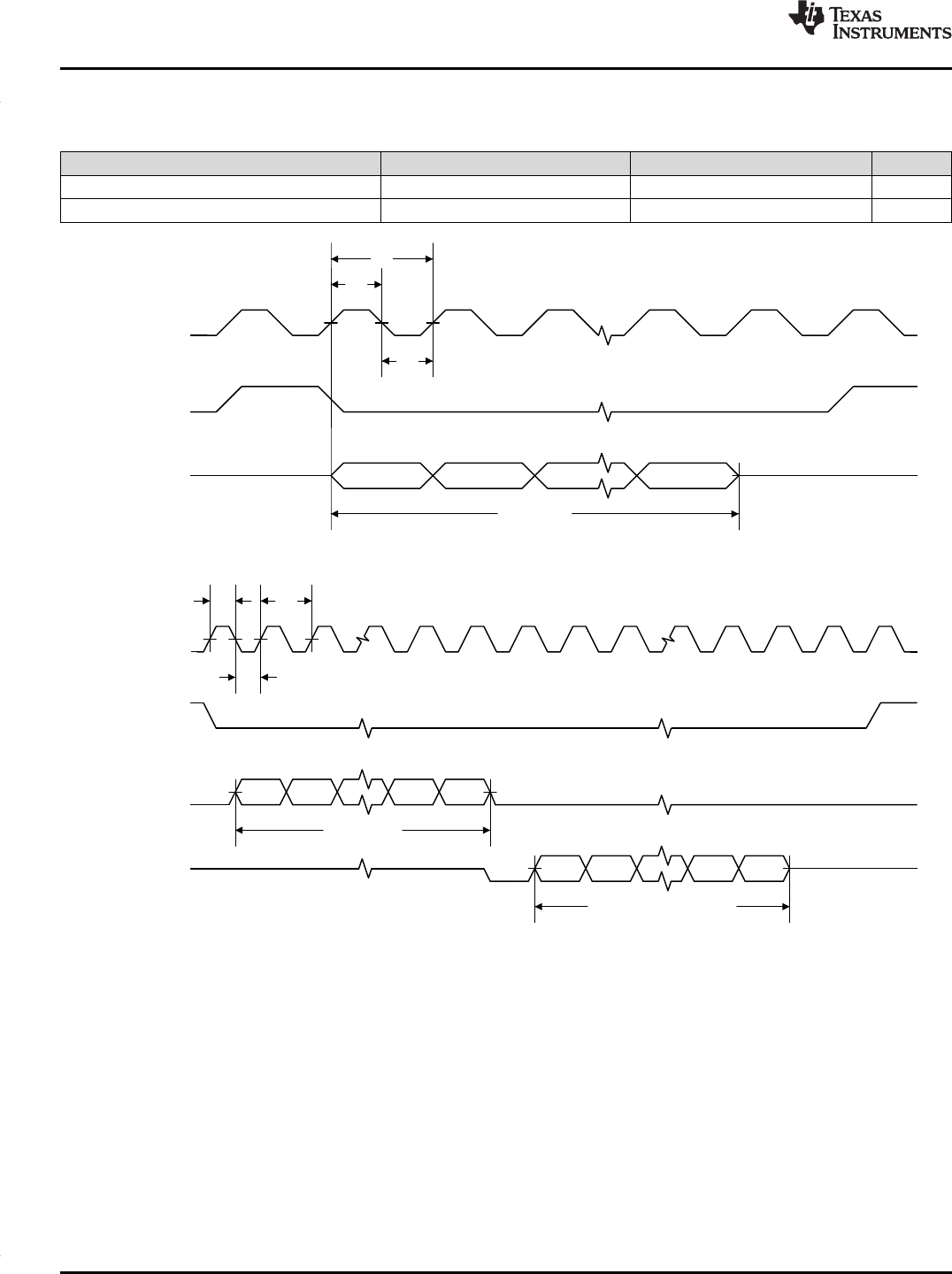
(4) Tc= 25°C, VDDS = 3.0 V, unless otherwise noted. Device operating as SLAVE. For SSI MASTER operation, see Section 5.26.
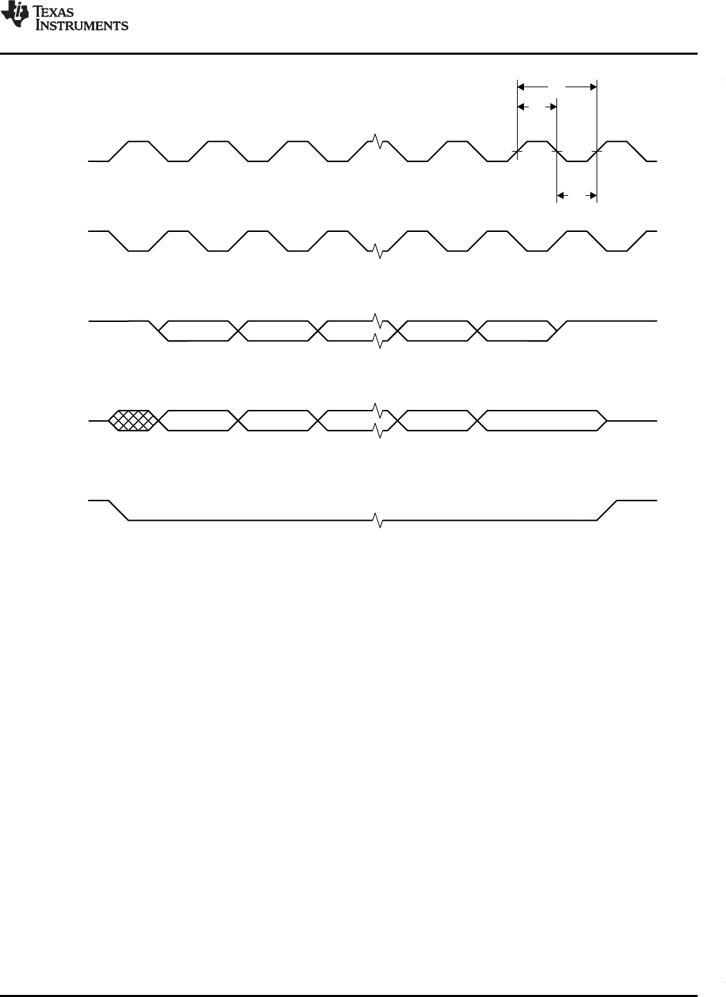
(5) Refer to SSI timing diagrams Figure 5-1,Figure 5-2, and Figure 5-3.
5.25 Timing Requirements
MIN NOM MAX UNIT
Rising supply-voltage slew rate 0 100 mV/µs
Falling supply-voltage slew rate 0 20 mV/µs
Falling supply-voltage slew rate, with low-power flash settings(1) 3 mV/µs
Positive temperature gradient in standby(2) No limitation for negative
temperature gradient, or
outside standby mode 5 °C/s
CONTROL INPUT AC CHARACTERISTICS(3)
RESET_N low duration 1 µs
SYNCHRONOUS SERIAL INTERFACE (SSI) (4)
S1 (SLAVE) (5) tclk_per SSIClk period 12 65024 system
clocks
S2 (5) tclk_high SSIClk high time 0.5 tclk_per
S3(5) tclk_low SSIClk low time 0.5 tclk_per
(1) Device operating as MASTER. For SSI SLAVE operation, see Section 5.25.
(2) Refer to SSI timing diagrams Figure 5-1,Figure 5-2, and Figure 5-3.
5.26 Switching Characteristics
Measured on the TI CC2650EM-5XD reference design with Tc= 25°C, VDDS = 3.0 V, unless otherwise noted.
PARAMETER TEST CONDITIONS MIN TYP MAX UNIT
WAKEUP AND TIMING
Idle →Active 14 µs
Standby →Active 151 µs
Shutdown →Active 1015 µs
SYNCHRONOUS SERIAL INTERFACE (SSI) (1)
S1 (TX only)(2) tclk_per (SSIClk period) One-way communication to SLAVE 4 65024 system
clocks
S1 (TX and RX)(2) tclk_per (SSIClk period) Normal duplex operation 8 65024 system
clocks
PRODUCTPREVIEW
0
SSIClk
SSIFss
SSITx
SSIRx
MSB LSB
MSB LSB
S2
S3
S1
8-bit control
4 to 16 bits output data
SSIClk
SSIFss
SSITx
SSIRx MSB LSB
S2
S3
S1
4 to 16 bits
18
CC2650MOD
SWRS187 –AUGUST 2016
www.ti.com
Submit Documentation Feedback
Product Folder Links: CC2650MOD
Specifications Copyright © 2016, Texas Instruments Incorporated
Switching Characteristics (continued)
Measured on the TI CC2650EM-5XD reference design with Tc= 25°C, VDDS = 3.0 V, unless otherwise noted.
PARAMETER TEST CONDITIONS MIN TYP MAX UNIT
S2 (2) tclk_high (SSIClk high time) 0.5 tclk_per
S3 (2) tclk_low(SSIClk low time) 0.5 tclk_per
Figure 5-1. SSI Timing for TI Frame Format (FRF = 01), Single Transfer Timing Measurement
Figure 5-2. SSI Timing for MICROWIRE Frame Format (FRF = 10), Single Transfer
PRODUCTPREVIEW
SSIClk
(SPO = 1)
SSITx
(Master)
SSIRx
(Slave) LSB
SSIClk
(SPO = 0)
S2
S1
SSIFss
LSB
S3
MSB
MSB
19
CC2650MOD
www.ti.com
SWRS187 –AUGUST 2016
Submit Documentation Feedback
Product Folder Links: CC2650MOD
SpecificationsCopyright © 2016, Texas Instruments Incorporated
Figure 5-3. SSI Timing for SPI Frame Format (FRF = 00), With SPH = 1
PRODUCTPREVIEW
Frequency (MHz)
Sensitivity Level (dBm)
2400 2410 2420 2430 2440 2450 2460 2470 2480
-101
-100
-99
-98
-97
-96
-95
D008
Sensitivity
Frequency (MHz)
Sensitivity Level (dBm)
2400 2410 2420 2430 2440 2450 2460 2470 2480
-99
-98.5
-98
-97.5
-97
-96.5
-96
-95.5
-95
D009
Sensitivity
VDDS (V)
Sensitivity (dBm)
1.8 2.3 2.8 3.3 3.8
-101
-100
-99
-98
-97
-96
-95
D006
BLE Sensitivity
VDDS (V)
Sensitivity (dBm)
1.9 2.4 2.9 3.4 3.8
-101
-100
-99
-98
-97
-96
-95
D007
IEEE 802.15.4 Sensitivity
Temperature (qC)
Sensitivity (dBm)
-40 -30 -20 -10 0 10 20 30 40 50 60 70 80
-99
-98
-97
-96
-95
-94
-93
D004
Sensitivity
Temperature (qC)
Sensitivity (dBm)
-40 -30 -20 -10 0 10 20 30 40 50 60 70 80
-103
-102
-101
-100
-99
-98
-97
-96
-95
D005
Sensitivity
20
CC2650MOD
SWRS187 –AUGUST 2016
www.ti.com
Submit Documentation Feedback
Product Folder Links: CC2650MOD
Specifications Copyright © 2016, Texas Instruments Incorporated
5.27 Typical Characteristics
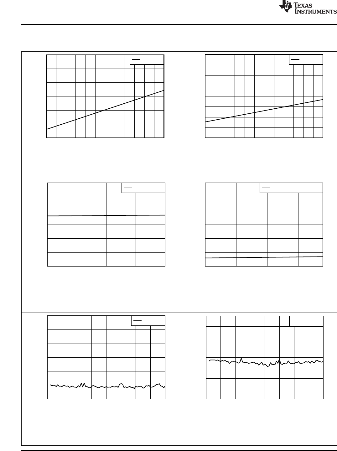
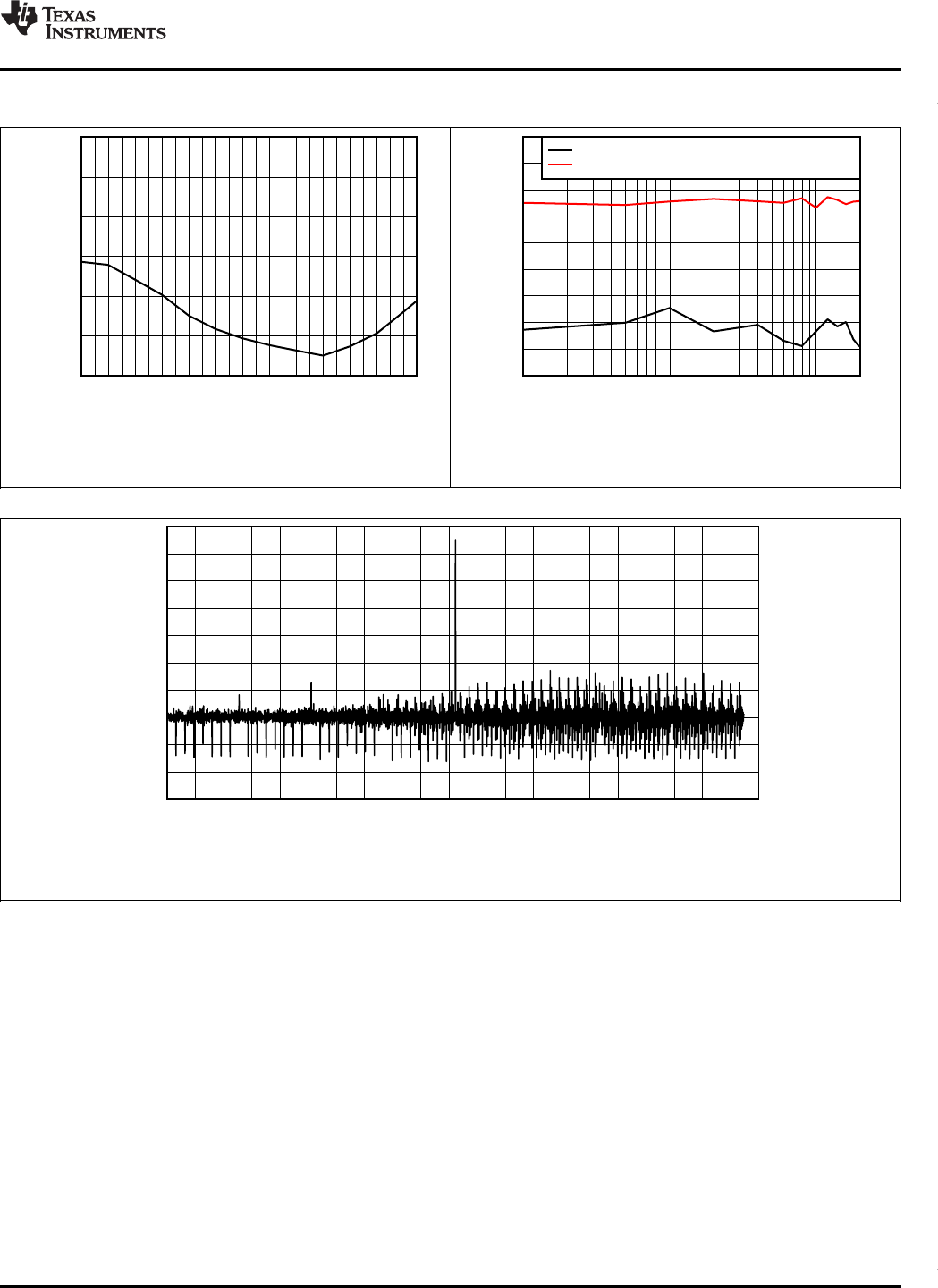
Figure 5-4. Bluetooth low energy Sensitivity vs Temperature Figure 5-5. IEEE 802.15.4 Sensitivity vs Temperature
Figure 5-6. Bluetooth low energy Sensitivity vs Supply Voltage
(VDDS) Figure 5-7. IEEE 802.15.4 Sensitivity vs Supply Voltage (VDDS)
Figure 5-8. IEEE 802.15.4 Sensitivity vs Channel Frequency Figure 5-9. Bluetooth low energy Sensitivity vs Channel
Frequency
PRODUCTPREVIEW
Voltage (V)
Current Consumption (mA)
1.75 2 2.25 2.5 2.75 3 3.25 3.5 3.75 4 4.25 4.5
4.5
5
5.5
6
6.5
7
7.5
8
8.5
9
9.5
10
10.5
D014
Temperature (qC)
RX Current (mA)
-40 -30 -20 -10 0 10 20 30 40 50 60 70 80
5.5
5.6
5.7
5.8
5.9
6
6.1
6.2
6.3
6.4
6.5
6.6
6.7
6.8
6.9
7
D015
RX Current
Frequency (MHz)
Output Power (dBm)
2400 2410 2420 2430 2440 2450 2460 2470 2480
-1
0
1
2
3
4
5
6
7
8
D012
5-dBm setting
VDDS (V)
TX Current (mA)
1.8 2 2.2 2.4 2.6 2.8 3 3.2 3.4 3.6 3.8
4
5
6
7
8
9
10
11
12
13
14
15
16
D013
5-dBm Setting
Temperature (qC)
Output Power (dBm)
-40 -30 -20 -10 0 10 20 30 40 50 60 70 80
0
1
2
3
4
5
6
D010
5-dBm Setting
VDDS (V)
Output power (dBm)
1.8 2.3 2.8 3.3 3.8
0
1
2
3
4
5
6
D011
5-dBm Setting
21
CC2650MOD
www.ti.com
SWRS187 –AUGUST 2016
Submit Documentation Feedback
Product Folder Links: CC2650MOD
SpecificationsCopyright © 2016, Texas Instruments Incorporated
Typical Characteristics (continued)
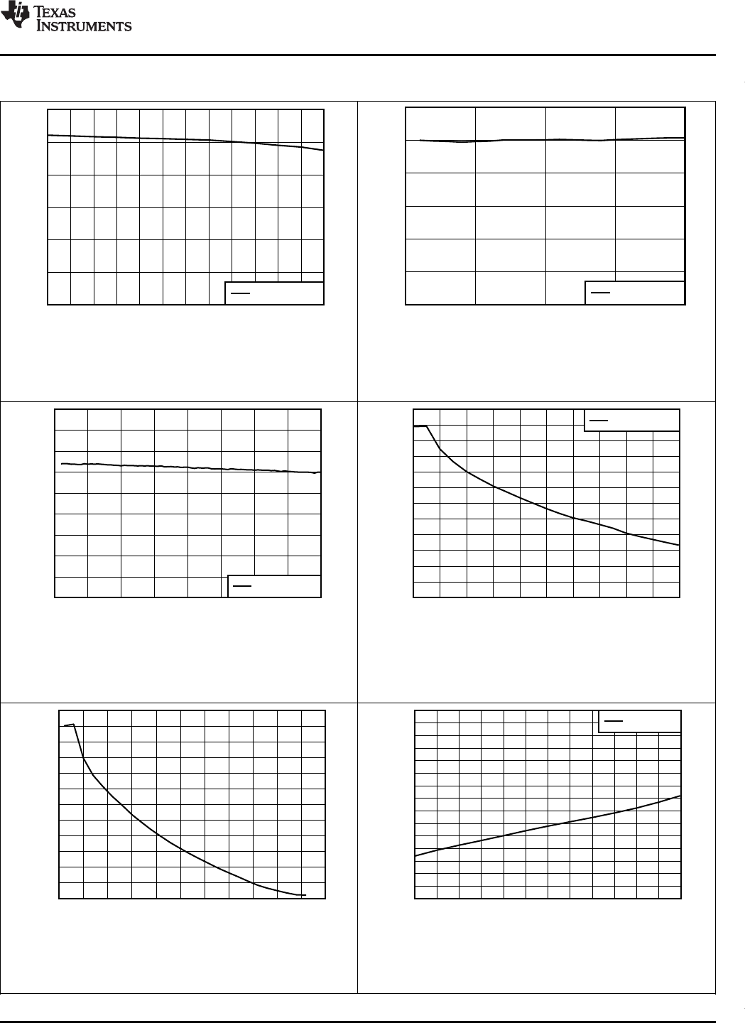
Figure 5-10. TX Output Power vs Temperature Figure 5-11. TX Output Power vs Supply Voltage (VDDS)
Figure 5-12. TX Output Power
vs Channel Frequency Figure 5-13. TX Current Consumption
vs Supply Voltage (VDDS)
Figure 5-14. RX Mode Current vs Supply Voltage (VDDS) Figure 5-15. RX Mode Current Consumption vs Temperature
PRODUCTPREVIEW
Input Frequency (Hz)
Effective Number of Bits
200300 500 1000 2000 5000 10000 20000 100000
9.4
9.6
9.8
10
10.2
10.4
10.6
10.8
11
11.2
11.4
D009
Fs= 200 kHz, No Averaging
Fs= 200 kHz, 32 samples averaging
VDDS (V)
ADC Code
1.8 2.3 2.8 3.3 3.8
1004.8
1005
1005.2
1005.4
1005.6
1005.8
1006
1006.2
1006.4
D012
VDDS (V)
Current Consumption (mA)
1.8 2.3 2.8 3.3 3.8
2
2.5
3
3.5
4
4.5
5
D007
Active Mode Current
Temperature (qC)
Current (uA)
-20 -10 0 10 20 30 40 50 60 70 80
0
0.5
1
1.5
2
2.5
3
3.5
4
D008
Standby Mode Current
Temperature (qC)
Active Mode Current Consumpstion (mA)
-40 -30 -20 -10 0 10 20 30 40 50 60 70 80
2.85
2.9
2.95
3
3.05
3.1
D006
Active Mode Current
Temperature (qC)
TX Current (mA)
-40 -30 -20 -10 0 10 20 30 40 50 60 70 80
0
2
4
6
8
10
12
D016
5-dBm Setting
22
CC2650MOD
SWRS187 –AUGUST 2016
www.ti.com
Submit Documentation Feedback
Product Folder Links: CC2650MOD
Specifications Copyright © 2016, Texas Instruments Incorporated
Typical Characteristics (continued)
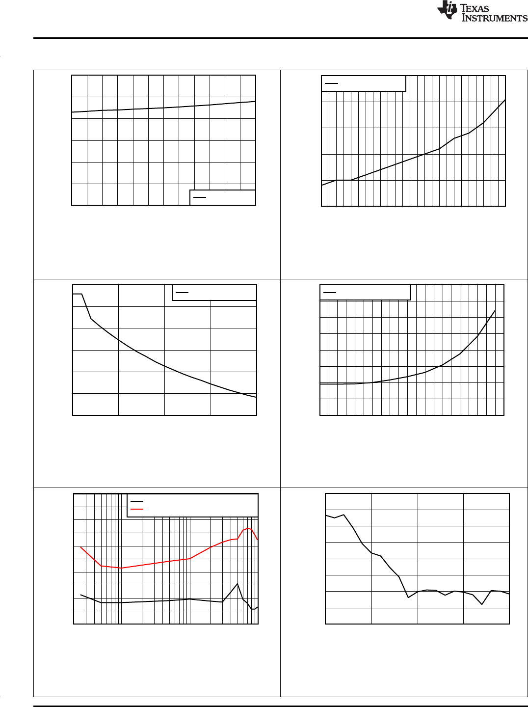
Figure 5-16. TX Mode Current Consumption vs Temperature Figure 5-17. Active Mode (MCU Running, No Peripherals)
Current Consumption vs Temperature
Figure 5-18. Active Mode (MCU Running, No Peripherals)
Current Consumption vs Supply Voltage (VDDS) Figure 5-19. Standby Mode Current Consumption
With RCOSC RTC vs Temperature
Figure 5-20. SoC ADC Effective Number of Bits vs Input
Frequency (Internal Reference, No Scaling) Figure 5-21. SoC ADC Output vs Supply Voltage (Fixed Input,
Internal Reference, No Scaling)
PRODUCTPREVIEW
ADC Code
DNL
0
200
400
600
800
1000
1200
1400
1600
1800
2000
2200
2400
2600
2800
3000
3200
3400
3600
3800
4000
4200
-1.5
-1
-0.5
0
0.5
1
1.5
2
2.5
3
3.5
D010
Temperature (qC)
ADC Code
-40 -30 -20 -10 0 10 20 30 40 50 60 70 80
1004.5
1005
1005.5
1006
1006.5
1007
1007.5
D013
Sampling Frequency (Hz)
ENOB
9.6
9.7
9.8
9.9
10
10.1
10.2
10.3
10.4
10.5
1k 10k 100k 200k
D009A
ENOB Internal Reference (No Averaging)
ENOB Internal Reference (32 Samples Averaging)
23
CC2650MOD
www.ti.com
SWRS187 –AUGUST 2016
Submit Documentation Feedback
Product Folder Links: CC2650MOD
SpecificationsCopyright © 2016, Texas Instruments Incorporated
Typical Characteristics (continued)
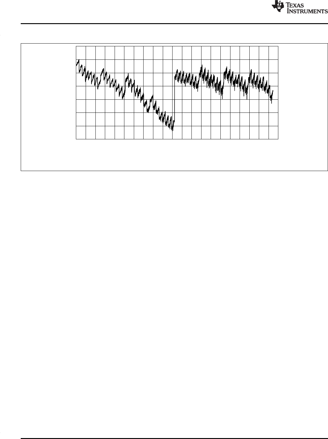
Figure 5-22. SoC ADC Output vs Temperature (Fixed Input,
Internal Reference, No Scaling) Figure 5-23. SoC ADC ENOB vs Sampling Frequency
(Input Frequency = FS / 10)
Figure 5-24. SoC ADC DNL vs ADC Code (Internal Reference, No Scaling)
PRODUCTPREVIEW
ADC Code
INL
0 200 400 600 800 1000 1200 1400 1600 1800 2000 2200 2400 2600 2800 3000 3200 3400 3600 3800 4000 4200
-4
-3
-2
-1
0
1
2
3
D011
24
CC2650MOD
SWRS187 –AUGUST 2016
www.ti.com
Submit Documentation Feedback
Product Folder Links: CC2650MOD
Specifications Copyright © 2016, Texas Instruments Incorporated
Typical Characteristics (continued)
Figure 5-25. SoC ADC INL vs ADC Code (Internal Reference, No Scaling)
PRODUCTPREVIEW
Main CPU:
128KB
Flash
Sensor Controller
cJTAG
20KB
SRAM
ROM
ARM®
Cortex®-M3
DC/DC converter
RF core
ARM®
Cortex®-M0
DSP Modem
4KB
SRAM
ROM
Sensor Controller Engine
2× Analog Comparators
12-bit ADC, 200ks/s
Constant Current Source
SPI / I2C Digital Sensor IF
2KB SRAM
Time to Digital Converter
General Peripherals / Modules
4× 32-bit Timers
2× SSI (SPI, µWire,TI)
Watchdog Timer
Temp. / Batt. Monitor
RTC
I2C
UART
I2S
10 / 15 / 31 GPIOs
AES
32 ch. µDMA
ADC
ADC
Digital PLL
SimpleLinkTM CC2650MOD
Wireless MCU Module
TRNG
8KB
Cache
24MHz Crystal
Oscillator
32.768kHz
Crystal
Oscillator RF Balun
Copyright © 2016, Texas Instruments Incorporated
25
CC2650MOD
www.ti.com
SWRS187 –AUGUST 2016
Submit Documentation Feedback
Product Folder Links: CC2650MOD
Detailed DescriptionCopyright © 2016, Texas Instruments Incorporated
6 Detailed Description
6.1 Overview
Section 6.2 shows the core modules of the CC2650MOD device.
6.2 Functional Block Diagram

PRODUCTPREVIEW
26
CC2650MOD
SWRS187 –AUGUST 2016
www.ti.com
Submit Documentation Feedback
Product Folder Links: CC2650MOD
Detailed Description Copyright © 2016, Texas Instruments Incorporated
6.3 Main CPU
The SimpleLink CC2650MOD Wireless MCU contains an ARM Cortex-M3 (CM3) 32-bit CPU, which runs
the application and the higher layers of the protocol stack.
The CM3 processor provides a high-performance, low-cost platform that meets the system requirements
of minimal memory implementation, and low-power consumption, while delivering outstanding
computational performance and exceptional system response to interrupts.
CM3 features include:
• 32-bit ARM Cortex-M3 architecture optimized for small-footprint embedded applications
• Outstanding processing performance combined with fast interrupt handling
• ARM Thumb®-2 mixed 16- and 32 bit instruction set delivers the high performance expected of a 32-bit
ARM core in a compact memory size usually associated with 8- and 16-bit devices, typically in the
range of a few kilobytes of memory for microcontroller-class applications:
– Single-cycle multiply instruction and hardware divide
– Atomic bit manipulation (bit-banding), delivering maximum memory use and streamlined peripheral
control
– Unaligned data access, enabling data to be efficiently packed into memory
• Fast code execution permits slower processor clock or increases sleep mode time
• Harvard architecture characterized by separate buses for instruction and data
• Efficient processor core, system, and memories
• Hardware division and fast digital-signal-processing oriented multiply accumulate
• Saturating arithmetic for signal processing
• Deterministic, high-performance interrupt handling for time-critical applications
• Enhanced system debug with extensive breakpoint and trace capabilities
• Serial wire trace reduces the number of pins required for debugging and tracing
• Migration from the ARM7™ processor family for better performance and power efficiency
• Optimized for single-cycle flash memory use
• Ultra-low power consumption with integrated sleep modes
• 1.25 DMIPS per MHz
6.4 RF Core
The RF Core contains an ARM®Cortex®-M0 processor that interfaces the analog RF and base-band
circuitries, handles data to and from the system side, and assembles the information bits in a given packet
structure. The RF core offers a high level, command-based API to the main CPU.
The RF core is capable of autonomously handling the time-critical aspects of the radio protocols (802.15.4
RF4CE and ZigBee, Bluetooth low energy) thus offloading the main CPU and leaving more resources for
the user application.
The RF core has a dedicated 4KB SRAM block and runs initially from separate ROM memory. The ARM
Cortex-M0 processor is not programmable by customers.

PRODUCTPREVIEW
27
CC2650MOD
www.ti.com
SWRS187 –AUGUST 2016
Submit Documentation Feedback
Product Folder Links: CC2650MOD
Detailed DescriptionCopyright © 2016, Texas Instruments Incorporated
6.5 Sensor Controller
The Sensor Controller contains circuitry that can be selectively enabled in standby mode. The peripherals
in this domain may be controlled by the Sensor Controller Engine, which is a proprietary power-optimized
CPU. This CPU can read and monitor sensors or perform other tasks autonomously, thereby significantly
reducing power consumption and offloading the main CM3 CPU.
The Sensor Controller is set up using a PC-based configuration tool, called Sensor Controller Studio, and
typical use cases may be (but are not limited to):
• Analog sensors using integrated ADC
• Digital sensors using GPIOs and bit-banged I2C or SPI
• UART communication for sensor reading or debugging
• Capacitive sensing
• Waveform generation
• Pulse counting
• Keyboard scan
• Quadrature decoder for polling rotation sensors
• Oscillator calibration
The peripherals in the Sensor Controller include the following:
• The low-power clocked comparator can be used to wake the device from any state in which the
comparator is active. A configurable internal reference can be used in conjunction with the comparator.
The output of the comparator can also be used to trigger an interrupt or the ADC.
• Capacitive sensing functionality is implemented through the use of a constant current source, a time-
to-digital converter, and a comparator. The continuous time comparator in this block can also be used
as a higher-accuracy alternative to the low-power clocked comparator. The Sensor Controller will take
care of baseline tracking, hysteresis, filtering and other related functions.
• The ADC is a 12-bit, 200 ksamples/s ADC with eight inputs and a built-in voltage reference. The ADC
can be triggered by many different sources, including timers, I/O pins, software, the analog
comparator, and the RTC.
• The Sensor Controller also includes a SPI/I2C digital interface.
• The analog modules can be connected to up to eight different GPIOs.
The peripherals in the Sensor Controller can also be controlled from the main application processor.

PRODUCTPREVIEW
28
CC2650MOD
SWRS187 –AUGUST 2016
www.ti.com
Submit Documentation Feedback
Product Folder Links: CC2650MOD
Detailed Description Copyright © 2016, Texas Instruments Incorporated
(1) Up to 13 pins can be connected to the Sensor Controller. Up to eight
of these pins can be connected to analog modules
Table 6-1. GPIOs Connected to the Sensor Controller(1)
ANALOG CAPABLE 16.9 × 11 MOH DIO NUMBER
Y 14
Y 13
Y 12
Y 11
Y 9
Y 10
Y 8
Y 7
N 4
N 3
N 2
N 1
N 0
6.6 Memory
The flash memory provides nonvolatile storage for code and data. The flash memory is in-system
programmable.
The SRAM (static RAM) can be used for both storage of data and execution of code and is split into two
4KB blocks and two 6KB blocks. Retention of the RAM contents in standby mode can be enabled or
disabled individually for each block to minimize power consumption. In addition, if flash cache is disabled,
the 8KB cache can be used as a general-purpose RAM.
The ROM provides preprogrammed embedded TI-RTOS kernel, Driverlib and lower layer protocol stack
software (802.15.4 MAC and Bluetooth low energy Controller). The ROM also contains a bootloader that
can be used to reprogram the device using SPI or UART.
6.7 Debug
The on-chip debug support is done through a dedicated cJTAG (IEEE 1149.7) or JTAG (IEEE 1149.1)
interface.

PRODUCTPREVIEW
29
CC2650MOD
www.ti.com
SWRS187 –AUGUST 2016
Submit Documentation Feedback
Product Folder Links: CC2650MOD
Detailed DescriptionCopyright © 2016, Texas Instruments Incorporated
(1) Not including RTOS overhead
(2) The Brown Out Detector is disabled between recharge periods in STANDBY. Lowering the supply voltage below the BOD threshold
between two recharge periods while in STANDBY may cause the BOD to lock the device upon wake-up until a Reset or POR releases
it. To avoid this, it is recommended that STANDBY mode is avoided if there is a risk that the supply voltage (VDDS) may drop below the
specified operating voltage range. For the same reason, it is also good practice to ensure that a power cycling operation, such as a
battery replacement, triggers a Power-on-reset by ensuring that the VDDS decoupling network is fully depleted before applying supply
voltage again (for example, inserting new batteries).
6.8 Power Management
To minimize power consumption, the CC2650MOD device supports a number of power modes and power
management features (see Table 6-2).
Table 6-2. Power Modes
MODE SOFTWARE CONFIGURABLE POWER MODES RESET PIN
HELD
ACTIVE IDLE STANDBY SHUTDOWN
CPU Active Off Off Off Off
Flash On Available Off Off Off
SRAM On On On Off Off
Radio Available Available Off Off Off
Supply System On On Duty Cycled Off Off
Current 1.45 mA + 31 µA/MHz 550 µA 1 µA 0.15 µA 0.1 µA
Wake-up time to CPU active(1) – 14 µs 151 µs 1015 µs 1015 µs
Register retention Full Full Partial No No
SRAM retention Full Full Full No No
High-speed clock XOSC_HF or
RCOSC_HF XOSC_HF or
RCOSC_HF Off Off Off
Low-speed clock XOSC_LF or
RCOSC_LF XOSC_LF or
RCOSC_LF XOSC_LF or
RCOSC_LF Off Off
Peripherals Available Available Off Off Off
Sensor Controller Available Available Available Off Off
Wake up on RTC Available Available Available Off Off
Wake up on pin edge Available Available Available Available Off
Wake up on reset pin Available Available Available Available Available
Brown Out Detector (BOD) Active Active Duty Cycled(2) Off N/A
Power On Reset (POR) Active Active Active Active N/A
In active mode, the application CM3 CPU is actively executing code. Active mode provides normal
operation of the processor and all of the peripherals that are currently enabled. The system clock can be
any available clock source (see Table 6-2).
In idle mode, all active peripherals can be clocked, but the Application CPU core and memory are not
clocked and no code is executed. Any interrupt event will bring the processor back into active mode.
In standby mode, only the always-on domain (AON) is active. An external wake event, RTC event, or
sensor-controller event is required to bring the device back to active mode. MCU peripherals with retention
do not need to be reconfigured when waking up again, and the CPU continues execution from where it
went into standby mode. All GPIOs are latched in standby mode.
In shutdown mode, the device is turned off entirely, including the AON domain and the Sensor Controller.
The I/Os are latched with the value they had before entering shutdown mode. A change of state on any
I/O pin, defined as a wake from Shutdown pin, wakes up the device and functions as a reset trigger. The
CPU can differentiate between a reset in this way, a reset-by-reset pin, or a power-on-reset by reading the
reset status register. The only state retained in this mode is the latched I/O state and the Flash memory
contents.

PRODUCTPREVIEW
30
CC2650MOD
SWRS187 –AUGUST 2016
www.ti.com
Submit Documentation Feedback
Product Folder Links: CC2650MOD
Detailed Description Copyright © 2016, Texas Instruments Incorporated
The Sensor Controller is an autonomous processor that can control the peripherals in the Sensor
Controller independently of the main CPU, which means that the main CPU does not have to wake up, for
example, to execute an ADC sample or poll a digital sensor over SPI. The main CPU saves both current
and wake-up time that would otherwise be wasted. The Sensor Controller Studio enables the user to
configure the sensor controller and choose which peripherals are controlled and which conditions wake up
the main CPU.
6.9 Clock Systems
The CC2650MOD device supports two external and two internal clock sources.
A 24-MHz crystal is required as the frequency reference for the radio. This signal is doubled internally to
create a 48-MHz clock.
The 32-kHz crystal is optional. Bluetooth low energy requires a slow-speed clock with better than
±500-ppm accuracy if the device is to enter any sleep mode while maintaining a connection. The internal
32-kHz RC oscillator can in some use cases be compensated to meet the requirements. The low-speed
crystal oscillator is designed for use with a 32-kHz watch-type crystal.
The internal high-speed oscillator (48 MHz) can be used as a clock source for the CPU subsystem.
The internal low-speed oscillator (32.768 kHz) can be used as a reference if the low-power crystal
oscillator is not used.
The 32-kHz clock source can be used as external clocking reference through GPIO.
6.10 General Peripherals and Modules
The I/O controller controls the digital I/O pins and contains multiplexer circuitry to allow a set of peripherals
to be assigned to I/O pins in a flexible manner. All digital I/Os are interrupt and wake-up capable, have a
programmable pullup and pulldown function and can generate an interrupt on a negative or positive edge
(configurable). When configured as an output, pins can function as either push-pull or open-drain. Five
GPIOs have high-drive capabilities (marked in bold in Section 4).
The SSIs are synchronous serial interfaces that are compatible with SPI, MICROWIRE, and TI's
synchronous serial interfaces. The SSIs support both SPI master and slave up to 4 MHz.
The UART implements a universal asynchronous receiver/transmitter function. It supports flexible baud-
rate generation up to a maximum of 3 Mbps .

PRODUCTPREVIEW
31
CC2650MOD
www.ti.com
SWRS187 –AUGUST 2016
Submit Documentation Feedback
Product Folder Links: CC2650MOD
Detailed DescriptionCopyright © 2016, Texas Instruments Incorporated
Timer 0 is a general-purpose timer module (GPTM), which provides two 16-bit timers. The GPTM can be
configured to operate as a single 32-bit timer, dual 16-bit timers or as a PWM module.
Timer 1, Timer 2, and Timer 3 are also GPTMs. Each of these timers is functionally equivalent to Timer 0.
In addition to these four timers, the RF core has its own timer to handle timing for RF protocols; the RF
timer can be synchronized to the RTC.
The I2C interface is used to communicate with devices compatible with the I2C standard. The I2C interface
is capable of 100-kHz and 400-kHz operation, and can serve as both I2C master and I2C slave.
The TRNG module provides a true, nondeterministic noise source for the purpose of generating keys,
initialization vectors (IVs), and other random number requirements. The TRNG is built on 24 ring
oscillators that create unpredictable output to feed a complex nonlinear combinatorial circuit.
The watchdog timer is used to regain control if the system fails due to a software error after an external
device fails to respond as expected. The watchdog timer can generate an interrupt or a reset when a
predefined time-out value is reached.
The device includes a direct memory access (µDMA) controller. The µDMA controller provides a way to
offload data transfer tasks from the CM3 CPU, allowing for more efficient use of the processor and the
available bus bandwidth. The µDMA controller can perform transfer between memory and peripherals. The
µDMA controller has dedicated channels for each supported on-chip module and can be programmed to
automatically perform transfers between peripherals and memory as the peripheral is ready to transfer
more data. Some features of the µDMA controller include the following (this is not an exhaustive list):
• Highly flexible and configurable channel operation of up to 32 channels
• Transfer modes: memory-to-memory, memory-to-peripheral, peripheral-to-memory, and peripheral-to-
peripheral
• Data sizes of 8, 16, and 32 bits
The AON domain contains circuitry that is always enabled, except for in Shutdown (where the digital
supply is off). This circuitry includes the following:
• The RTC can be used to wake the device from any state where it is active. The RTC contains three
compare and one capture registers. With software support, the RTC can be used for clock and
calendar operation. The RTC is clocked from the 32-kHz RC oscillator or crystal. The RTC can also be
compensated to tick at the correct frequency even when the internal 32-kHz RC oscillator is used
instead of a crystal.
• The battery monitor and temperature sensor are accessible by software and give a battery status
indication as well as a coarse temperature measure.

PRODUCTPREVIEW
32
CC2650MOD
SWRS187 –AUGUST 2016
www.ti.com
Submit Documentation Feedback
Product Folder Links: CC2650MOD
Detailed Description Copyright © 2016, Texas Instruments Incorporated
6.11 System Architecture
Depending on the product configuration, CC26xx can function either as a Wireless Network Processor
(WNP—an IC running the wireless protocol stack, with the application running on a separate MCU), or as
a System-on-Chip (SoC), with the application and protocol stack running on the ARM CM3 core inside the
device.
In the first case, the external host MCU communicates with the device using SPI or UART. In the second
case, the application must be written according to the application framework supplied with the wireless
protocol stack.
6.12 Certification
The CC2650MODA module is certified to the standards listed in Table 6-3 (with IDs where applicable):
Table 6-3. CC2650MODA List of Certifications
Regulatory Body Specification ID (if applicable)
FCC (USA) Part 15C:2015+MPE FCC 1.1307 RF Exposure (Bluetooth)FCC ID: ZAT26M1
Part 15C:2015+MPE FCC 1.1307 RF Exposure (802.15.4)
IC (Canada) RSS-247 (Bluetooth)ID: 451H-26M1
RSS-247 (802.15.4)
ETSI/CE (Europe)
EN300328 v1.9.1 (Bluetooth)
EN300328 v1.9.1 (802.15.4)
IEC/EN62479:Ver 2010 (MPE) (replacing EN50371)
EN301489-1 v1.9.2:2011
EN301489-3 v1.6.1:2013
EN301489-17 v2.2.1:2012 (EMC)
EN55022:2010+AC:2011
EN55024:2011
EN60950-1: A2/2013
Japan MIC JRF-STD-66
JATE
6.12.1 Federal Communications Commission Statement
You are cautioned that changes or modifications not expressly approved by the part responsible for
compliance could void the user’s authority to operate the equipment.
This device complies with Part 15 of the FCC Rules. Operation is subject to the following two
conditions:
1. This device may not cause harmful interference and
2. This device must accept any interference received, including interference that may cause undesired
operation of the device.
FCC RF Radiation Exposure Statement:
This equipment complies with FCC radiation exposure limits set forth for an uncontrolled environment. End
users must follow the specific operating instructions for satisfying RF exposure limits. This transmitter
must not be colocated or operating in conjunction with any other antenna or transmitter.

PRODUCTPREVIEW
33
CC2650MOD
www.ti.com
SWRS187 –AUGUST 2016
Submit Documentation Feedback
Product Folder Links: CC2650MOD
Detailed DescriptionCopyright © 2016, Texas Instruments Incorporated
6.12.2 Canada, Industry Canada (IC)
This device complies with Industry Canada licence-exempt RSS standard(s).
Operation is subject to the following two conditions:
1. This device may not cause interference, and
2. This device must accept any interference, including interference that may cause undesired operation of
the device
Le présent appareil est conforme aux CNR d'Industrie Canada applicables aux appareils radio
exempts de licence
L'exploitation est autorisée aux deux conditions suivantes:
1. l'appareil ne doit pas produire de brouillage, et
2. l'utilisateur de l'appareil doit accepter tout brouillage radioélectrique subi, même si le brouillage est
susceptible d'en compromettre le fonctionnement.
IC RF Radiation Exposure Statement:
To comply with IC RF exposure requirements, this device and its antenna must not be co-located or
operating in conjunction with any other antenna or transmitter.
Pour se conformer aux exigences de conformité RF canadienne l'exposition, cet appareil et son antenne
ne doivent pas étre co-localisés ou fonctionnant en conjonction avec une autre antenne ou transmetteur.
6.13 End Product Labeling
This module is designed to comply with the FCC statement, FCC ID : ZAT26M1. The host system using
this module must display a visible label indicating the following text:
"Contains FCC ID: ZAT26M1"
This module is designed to comply with the IC statement, IC : 451H-26M1. The host system using this
module must display a visible label indicating the following text:
"Contains IC: 451H-26M1"
6.14 Manual Information to the End User
The OEM integrator has to be aware not to provide information to the end user regarding how to install or
remove this RF module in the user’s manual of the end product which integrates this module.
The end user manual shall include all required regulatory information/warning as shown in this manual.
PRODUCTPREVIEW
nReset
JTAG-TCK
JTAG-TMS
DIO0
DIO1
DIO2
DIO3
DIO4
DIO5
DIO6
DIO7
DIO8
DIO9
DIO10
DIO11
DIO12
DIO13
DIO14
VDDS
VDDS
CC2650MODAMOH
U1
NC_2 2
DIO_0
4
DIO_1
5
DIO_2
6
DIO_3
7
DIO_4
8
DIO_5/JTAG_TDO
11
DIO_6/JTAG_TDI
12
DIO_7
14
DIO_8
15
DIO_9
16
DIO_10
17
DIO_11
18
DIO_12
19
DIO_13
20
DIO_14
21
VDDS 22
nRESET
13
JTAG_TMSC
9JTAG_TCKC
10
VDDS 23
NC_24 24
GND
1
GND
3
GND
25
EGP 26
EGP 27
EGP 28
EGP 29
R28
100k
Copyright © 2016, Texas Instruments Incorporated
34
CC2650MOD
SWRS187 –AUGUST 2016
www.ti.com
Submit Documentation Feedback
Product Folder Links: CC2650MOD
Application, Implementation, and Layout Copyright © 2016, Texas Instruments Incorporated
7 Application, Implementation, and Layout
NOTE
Information in the following applications sections is not part of the TI component
specification, and TI does not warrant its accuracy or completeness. TI's customers are
responsible for determining suitability of components for their purposes. Customers should
validate and test their design implementation to confirm system functionality.
7.1 Application Information
7.1.1 Typical Application Circuit
No external components are required for the operation of the CC2650MOD device. Figure 7-1 shows the
application circuit.
Figure 7-1. CC2650MOD Application Circuit

PRODUCTPREVIEW
SimpleLink™ Multistandard
Wireless MCU
DEVICE FAMILY
PREFIX
CC2650 MOD
X = Experimental device
Blank = Qualified device
MOH
A
ROM version 1
Flash = 128KB
DEVICE
PACKAGE DESIGNATOR
MOH = 29-pin Module
MOD = Module
35
CC2650MOD
www.ti.com
SWRS187 –AUGUST 2016
Submit Documentation Feedback
Product Folder Links: CC2650MOD
Device and Documentation SupportCopyright © 2016, Texas Instruments Incorporated
8 Device and Documentation Support
8.1 Device Nomenclature
To designate the stages in the product development cycle, TI assigns prefixes to all part numbers and/or
date-code. Each device has one of three prefixes/identifications: X, P, or null (no prefix) (for example,
CC2650MOD is in production; therefore, no prefix/identification is assigned).
Device development evolutionary flow:
XExperimental device that is not necessarily representative of the final device's electrical
specifications and may not use production assembly flow.
PPrototype device that is not necessarily the final silicon die and may not necessarily meet
final electrical specifications.
null Production version of the silicon die that is fully qualified.
Production devices have been characterized fully, and the quality and reliability of the device have been
demonstrated fully. TI's standard warranty applies.
Predictions show that prototype devices (X or P) have a greater failure rate than the standard production
devices. Texas Instruments recommends that these devices not be used in any production system
because their expected end-use failure rate still is undefined. Only qualified production devices are to be
used.
TI device nomenclature also includes a suffix with the device family name. This suffix indicates the
package type (for example, MOH).
For orderable part numbers of CC2650MOD devices in the MOH package type, see the Package Option
Addendum of this document, the TI website (www.ti.com), or contact your TI sales representative.
Figure 8-1. Device Nomenclature

PRODUCTPREVIEW
36
CC2650MOD
SWRS187 –AUGUST 2016
www.ti.com
Submit Documentation Feedback
Product Folder Links: CC2650MOD
Device and Documentation Support Copyright © 2016, Texas Instruments Incorporated
8.2 Tools and Software
TI offers an extensive line of development tools, including tools to evaluate the performance of the
processors, generate code, develop algorithm implementations, and fully integrate and debug software
and hardware modules.
The following products support development of the CC2650MOD device applications:
Software Tools:
SmartRF Studio 7:
SmartRF Studio is a PC application that helps designers of radio systems to easily evaluate the RF-IC at
an early stage in the design process.
• Test functions for sending and receiving radio packets, continuous wave transmit and receive
• Evaluate RF performance on custom boards by wiring it to a supported evaluation board or debugger
• Can also be used without any hardware, but then only to generate, edit and export radio configuration
settings
• Can be used in combination with several development kits for TI's CCxxxx RF-ICs
Sensor Controller Studio:
Sensor Controller Studio provides a development environment for the CC26xx Sensor Controller. The
Sensor Controller is a proprietary, power-optimized CPU in the CC26xx, which can perform simple
background tasks autonomously and independent of the System CPU state.
• Allows for Sensor Controller task algorithms to be implemented using a C-like programming language
• Outputs a Sensor Controller Interface driver, which incorporates the generated Sensor Controller
machine code and associated definitions
• Allows for rapid development by using the integrated Sensor Controller task testing and debugging
functionality. This allows for live visualization of sensor data and algorithm verification.
IDEs and Compilers:
Code Composer Studio:
• Integrated development environment with project management tools and editor
• Code Composer Studio (CCS) 6.1 and later has built-in support for the CC26xx device family
• Best support for XDS debuggers; XDS100v3, XDS110 and XDS200
• High integration with TI-RTOS with support for TI-RTOS Object View
IAR Embedded Workbench for ARM
• Integrated development environment with project management tools and editor
• IAR EWARM 7.30.3 and later has built-in support for the CC26xx device family
• Broad debugger support, supporting XDS100v3, XDS200, IAR I-Jet and Segger J-Link
• Integrated development environment with project management tools and editor
• RTOS plugin is available for TI-RTOS
For a complete listing of development-support tools for the CC2650MOD platform, visit the Texas
Instruments website at www.ti.com. For information on pricing and availability, contact the nearest TI field
sales office or authorized distributor.

PRODUCTPREVIEW
37
CC2650MOD
www.ti.com
SWRS187 –AUGUST 2016
Submit Documentation Feedback
Product Folder Links: CC2650MOD
Device and Documentation SupportCopyright © 2016, Texas Instruments Incorporated
8.3 Documentation Support
The following documents describe the CC2650MOD device. Copies of these documents are available on
the Internet at www.ti.com.
CC26xx SimpleLink™ Wireless MCU Technical Reference Manual
CC26xx SimpleLink™ Wireless MCU Errata
8.3.1 Community Resources
The following links connect to TI community resources. Linked contents are provided "AS IS" by the
respective contributors. They do not constitute TI specifications and do not necessarily reflect TI's views;
see TI's Terms of Use.
TI E2E™ Online Community TI's Engineer-to-Engineer (E2E) Community. Created to foster
collaboration among engineers. At e2e.ti.com, you can ask questions, share knowledge,
explore ideas and help solve problems with fellow engineers.
TI Embedded Processors Wiki Texas Instruments Embedded Processors Wiki. Established to help
developers get started with Embedded Processors from Texas Instruments and to foster
innovation and growth of general knowledge about the hardware and software surrounding
these devices.
8.4 Texas Instruments Low-Power RF Website
TI's Low-Power RF website has all the latest products, application and design notes, FAQ section, news
and events updates. Go to www.ti.com/lprf.
8.5 Low-Power RF eNewsletter
The Low-Power RF eNewsletter is up-to-date on new products, news releases, developers’ news, and
other news and events associated with low-power RF products from TI. The Low-Power RF eNewsletter
articles include links to get more online information.
Sign up at: www.ti.com/lprfnewsletter

PRODUCTPREVIEW
38
CC2650MOD
SWRS187 –AUGUST 2016
www.ti.com
Submit Documentation Feedback
Product Folder Links: CC2650MOD
Device and Documentation Support Copyright © 2016, Texas Instruments Incorporated
8.6 Community Resources
The following links connect to TI community resources. Linked contents are provided "AS IS" by the
respective contributors. They do not constitute TI specifications and do not necessarily reflect TI's views;
see TI's Terms of Use.
TI E2E™ Online Community TI's Engineer-to-Engineer (E2E) Community. Created to foster
collaboration among engineers. At e2e.ti.com, you can ask questions, share knowledge,
explore ideas and help solve problems with fellow engineers.
TI Embedded Processors Wiki Texas Instruments Embedded Processors Wiki. Established to help
developers get started with Embedded Processors from Texas Instruments and to foster
innovation and growth of general knowledge about the hardware and software surrounding
these devices.
Low-Power RF Online Community Wireless Connectivity Section of the TI E2E Support Community
• Forums, videos, and blogs
• RF design help
• E2E interaction
Join here.
Low-Power RF Developer Network Texas Instruments has launched an extensive network of low-power
RF development partners to help customers speed up their application development. The
network consists of recommended companies, RF consultants, and independent design
houses that provide a series of hardware module products and design services, including:
• RF circuit, low-power RF, and ZigBee design services
• Low-power RF and ZigBee module solutions and development tools
• RF certification services and RF circuit manufacturing
For help with modules, engineering services or development tools:
Search the Low-Power RF Developer Network to find a suitable partner.
www.ti.com/lprfnetwork
8.7 Additional Information
Texas Instruments offers a wide selection of cost-effective, low-power RF solutions for proprietary and
standard-based wireless applications for use in industrial and consumer applications. The selection
includes RF transceivers, RF transmitters, RF front ends, and Systems-on-Chips as well as various
software solutions for the sub-1-GHz and 2.4-GHz frequency bands.
In addition, Texas Instruments provides a large selection of support collateral such as development tools,
technical documentation, reference designs, application expertise, customer support, third-party and
university programs.
The Low-Power RF E2E Online Community provides technical support forums, videos and blogs, and the
chance to interact with engineers from all over the world.
With a broad selection of product solutions, end-application possibilities, and a range of technical support,
Texas Instruments offers the broadest low-power RF portfolio.
8.8 Trademarks
IAR Embedded Workbench is a registered trademark of IAR Systems AB.
SmartRF, Code Composer Studio, SimpleLink, TI-RTOS, E2E are trademarks of Texas Instruments.
ARM7 is a trademark of ARM Limited.
ARM, Cortex are registered trademarks of ARM Limited (or its subsidiaries).
ARM Thumb is a registered trademark of ARM Limited.
Bluetooth is a registered trademark of Bluetooth SIG, Inc.
CoreMark is a registered trademark of Embedded Microprocessor Benchmark Consortium.
IEEE Std 1241 is a trademark of Institute of Electrical and Electronics Engineers, Incorporated.
ZigBee is a registered trademark of ZigBee Alliance, Inc.

PRODUCTPREVIEW
39
CC2650MOD
www.ti.com
SWRS187 –AUGUST 2016
Submit Documentation Feedback
Product Folder Links: CC2650MOD
Mechanical Packaging and Orderable InformationCopyright © 2016, Texas Instruments Incorporated
8.9 Electrostatic Discharge Caution
This integrated circuit can be damaged by ESD. Texas Instruments recommends that all integrated circuits be handled with
appropriate precautions. Failure to observe proper handling and installation procedures can cause damage.
ESD damage can range from subtle performance degradation to complete device failure. Precision integrated circuits may be more
susceptible to damage because very small parametric changes could cause the device not to meet its published specifications.
8.10 Export Control Notice
Recipient agrees to not knowingly export or re-export, directly or indirectly, any product or technical data
(as defined by the U.S., EU, and other Export Administration Regulations) including software, or any
controlled product restricted by other applicable national regulations, received from Disclosing party under
this Agreement, or any direct product of such technology, to any destination to which such export or re-
export is restricted or prohibited by U.S. or other applicable laws, without obtaining prior authorization from
U.S. Department of Commerce and other competent Government authorities to the extent required by
those laws.
8.11 Glossary
SLYZ022 —TI Glossary.
This glossary lists and explains terms, acronyms and definitions.
9 Mechanical Packaging and Orderable Information
9.1 Packaging Information
The following pages include mechanical packaging and orderable information. This information is the most
current data available for the designated devices. This data is subject to change without notice and
revision of this document. For browser-based versions of this data sheet, refer to the left-hand navigation.

IMPORTANT NOTICE
Texas Instruments Incorporated and its subsidiaries (TI) reserve the right to make corrections, enhancements, improvements and other
changes to its semiconductor products and services per JESD46, latest issue, and to discontinue any product or service per JESD48, latest
issue. Buyers should obtain the latest relevant information before placing orders and should verify that such information is current and
complete. All semiconductor products (also referred to herein as “components”) are sold subject to TI’s terms and conditions of sale
supplied at the time of order acknowledgment.
TI warrants performance of its components to the specifications applicable at the time of sale, in accordance with the warranty in TI’s terms
and conditions of sale of semiconductor products. Testing and other quality control techniques are used to the extent TI deems necessary
to support this warranty. Except where mandated by applicable law, testing of all parameters of each component is not necessarily
performed.
TI assumes no liability for applications assistance or the design of Buyers’ products. Buyers are responsible for their products and
applications using TI components. To minimize the risks associated with Buyers’ products and applications, Buyers should provide
adequate design and operating safeguards.
TI does not warrant or represent that any license, either express or implied, is granted under any patent right, copyright, mask work right, or
other intellectual property right relating to any combination, machine, or process in which TI components or services are used. Information
published by TI regarding third-party products or services does not constitute a license to use such products or services or a warranty or
endorsement thereof. Use of such information may require a license from a third party under the patents or other intellectual property of the
third party, or a license from TI under the patents or other intellectual property of TI.
Reproduction of significant portions of TI information in TI data books or data sheets is permissible only if reproduction is without alteration
and is accompanied by all associated warranties, conditions, limitations, and notices. TI is not responsible or liable for such altered
documentation. Information of third parties may be subject to additional restrictions.
Resale of TI components or services with statements different from or beyond the parameters stated by TI for that component or service
voids all express and any implied warranties for the associated TI component or service and is an unfair and deceptive business practice.
TI is not responsible or liable for any such statements.
Buyer acknowledges and agrees that it is solely responsible for compliance with all legal, regulatory and safety-related requirements
concerning its products, and any use of TI components in its applications, notwithstanding any applications-related information or support
that may be provided by TI. Buyer represents and agrees that it has all the necessary expertise to create and implement safeguards which
anticipate dangerous consequences of failures, monitor failures and their consequences, lessen the likelihood of failures that might cause
harm and take appropriate remedial actions. Buyer will fully indemnify TI and its representatives against any damages arising out of the use
of any TI components in safety-critical applications.
In some cases, TI components may be promoted specifically to facilitate safety-related applications. With such components, TI’s goal is to
help enable customers to design and create their own end-product solutions that meet applicable functional safety standards and
requirements. Nonetheless, such components are subject to these terms.
No TI components are authorized for use in FDA Class III (or similar life-critical medical equipment) unless authorized officers of the parties
have executed a special agreement specifically governing such use.
Only those TI components which TI has specifically designated as military grade or “enhanced plastic” are designed and intended for use in
military/aerospace applications or environments. Buyer acknowledges and agrees that any military or aerospace use of TI components
which have not been so designated is solely at the Buyer's risk, and that Buyer is solely responsible for compliance with all legal and
regulatory requirements in connection with such use.
TI has specifically designated certain components as meeting ISO/TS16949 requirements, mainly for automotive use. In any case of use of
non-designated products, TI will not be responsible for any failure to meet ISO/TS16949.
Products Applications
Audio www.ti.com/audio Automotive and Transportation www.ti.com/automotive
Amplifiers amplifier.ti.com Communications and Telecom www.ti.com/communications
Data Converters dataconverter.ti.com Computers and Peripherals www.ti.com/computers
DLP® Products www.dlp.com Consumer Electronics www.ti.com/consumer-apps
DSP dsp.ti.com Energy and Lighting www.ti.com/energy
Clocks and Timers www.ti.com/clocks Industrial www.ti.com/industrial
Interface interface.ti.com Medical www.ti.com/medical
Logic logic.ti.com Security www.ti.com/security
Power Mgmt power.ti.com Space, Avionics and Defense www.ti.com/space-avionics-defense
Microcontrollers microcontroller.ti.com Video and Imaging www.ti.com/video
RFID www.ti-rfid.com
OMAP Applications Processors www.ti.com/omap TI E2E Community e2e.ti.com
Wireless Connectivity www.ti.com/wirelessconnectivity
Mailing Address: Texas Instruments, Post Office Box 655303, Dallas, Texas 75265
Copyright © 2016, Texas Instruments Incorporated