Texas Instruments RFM003B Inductive Reader Module User Manual RI RFM 003B Series 2000 Reader System Mini RFM
Texas Instruments Inc Inductive Reader Module RI RFM 003B Series 2000 Reader System Mini RFM
UserManual.wiki
>
Texas Instruments
>
RFM003B User Manual
Manaul
Navigation menu
Upload a User Manual
Namespaces
Wiki Guide
HTML
PDF
Info
Views
User Manual
Discussion / Help
Navigation
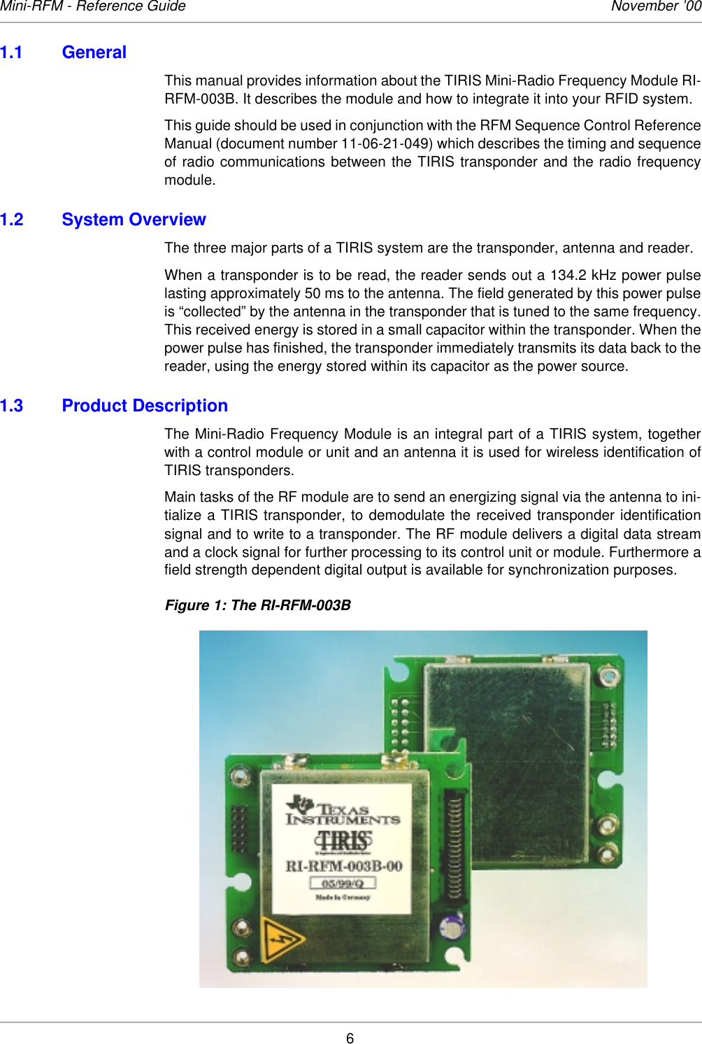
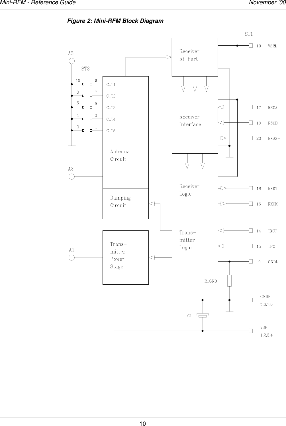
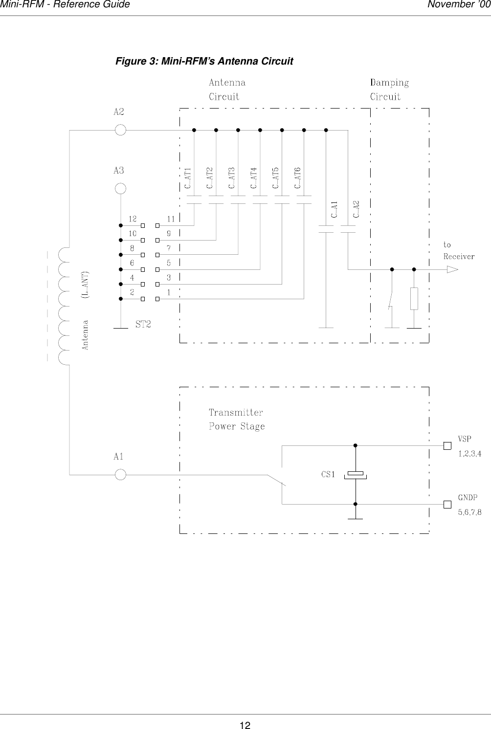
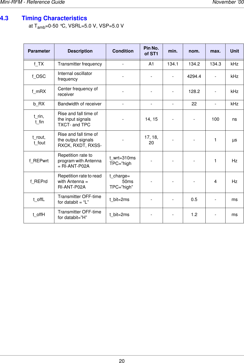
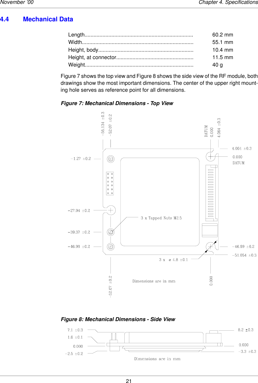
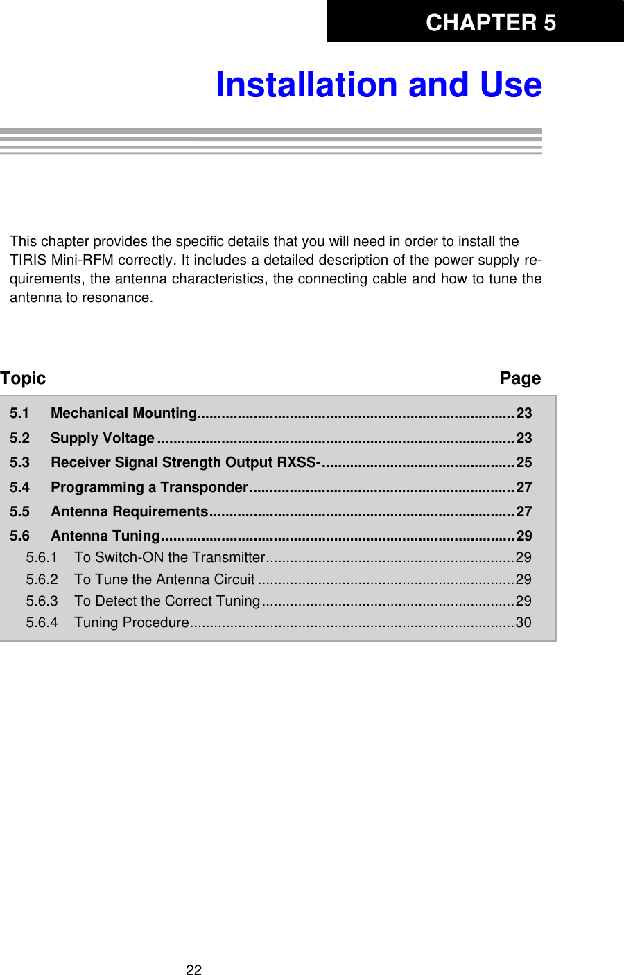
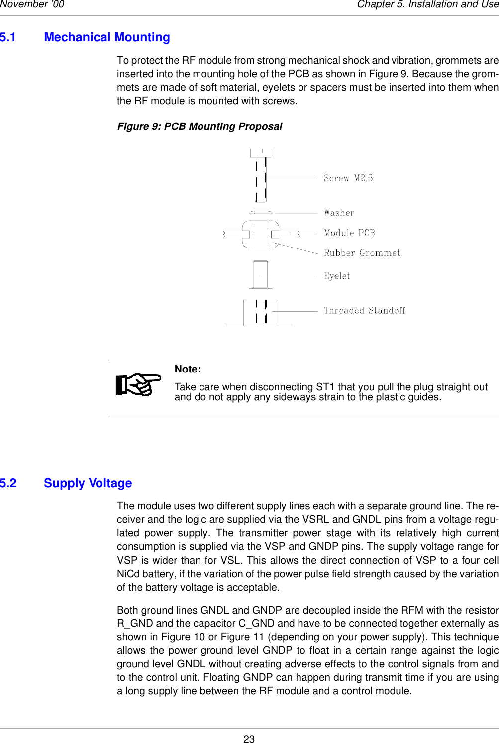
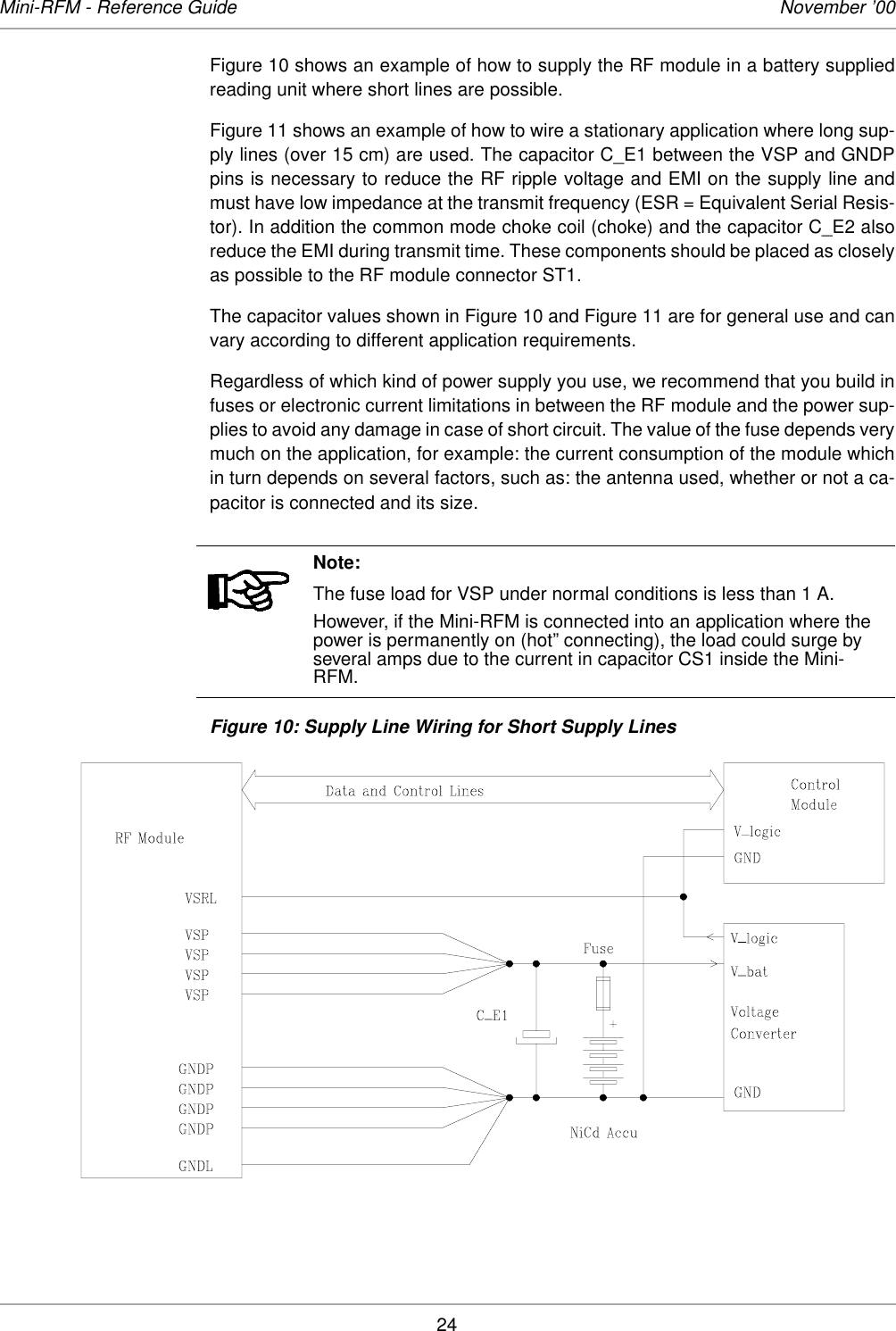
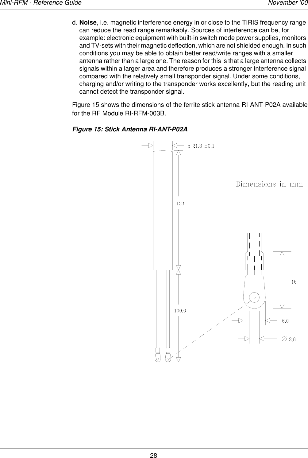
![19November ’00 Chapter 4. SpecificationsFigure 6: Maximum Supply Current I_VSP versus t_off (Power Stage)Time t_off between 2 charge pulses of 50 ms [ms]Values in brackets ( ) are for time t_off between 2 write cyclesI_IL Low level input current for RSCA and RSCB V_IL=0V 17, 19 - -30 µAI_IH High level input current for RSCA and RSCB V_IH=5V 17, 19 - - 30 µAV_OH High level output voltage for RXCK, RXDT and RXSS- I_OH=-2mA 16, 18, 20 2,4--VV_OH High level output voltage for RXCK, RXDT and RXSS- I_OH=-1mA 16, 18, 20 4.0--VV_OL Low level output voltage for RXCK, RXDT and RXSS- I_OL=-2mA 16, 18, 20 --0.5VR_GND Decoupling resistor between GNDL and GNDP -9 to 5,6,7,8 -33-OhmParameter Description Condition Pin No. of ST2 min. nom. max UnitC_A1 +C_A2 Antenna capacity without tuning cap. A2 10.6 - 11.8 nFC_AT6 Antenna tuning capacity weighted 32 - 1 1425 1500 1575 pFC_AT5 Antenna tuning capacity weighted 16 - 3 740 780 820 pFC_AT4 Antenna tuning capacity weighted 8 - 5 370 391 410 pFC_AT3 Antenna tuning capacity weighted 4 - 7 209 220 231 pFC_AT2 Antenna tuning capacity weighted 2 - 9 95 100 105 pFC_AT1 Antenna tuning capacity weighted 1 - 11 50 56 64 pFParameter Description Condition Pin No. of ST1 min. nom. max Unit1.81.51.20.90.60.3 050(250) 100(400) 150(550) 200(700) 250(850)0I_VSP_max [A]](https://usermanual.wiki/Texas-Instruments/RFM003B/User-Guide-182227-Page-19.png)