Texas Instruments RFM003B Inductive Reader Module User Manual RI RFM 003B Series 2000 Reader System Mini RFM
Texas Instruments Inc Inductive Reader Module RI RFM 003B Series 2000 Reader System Mini RFM
Manaul

1
November ’00 Preface
Series 2000 Reader System
Mini-RFM RI-RFM-003B
Reference Guide
11-06-29-030 November 2000

2
Mini-RFM - Reference Guide November ’00
Edition Three - November 2000
This is the third edition of this manual, it describes the following equipment:
TIRIS Mini-Radio Frequency Module RI-RFM-003B
Texas Instruments (TI) reserves the right to make changes to its products or services
or to discontinue any product or service at any time without notice. TI provides cus-
tomer assistance in various technical areas, but does not have full access to data
concerning the use and applications of customer's products.
Therefore, TI assumes no liability and is not responsible for customer applications or
product or software design or performance relating to systems or applications incor-
porating TI products. In addition, TI assumes no liability and is not responsible for
infringement of patents and/or any other intellectual or industrial property rights of
third parties, which may result from assistance provided by TI.
TI products are not designed, intended, authorized or warranted to be suitable for life
support applications or any other life critical applications which could involve poten-
tial risk of death, personal injury or severe property or environmental damage.
The TIRIS logo and the word TIRIS are registered trademarks of Texas Instruments
Incorporated.
Copyright 2000 Texas Instruments Incorporated (TI)
This document may be downloaded onto a computer, stored and duplicated as nec-
essary to support the use of the related TI products. Any other type of duplication,
circulation or storage on data carriers in any manner not authorized by TI represents
a violation of the applicable copyright laws and shall be prosecuted.
PREFACE
3
Read This First
About This Guide
This manual describes the TIRIS Mini-Radio Frequency Module (Mini-RFM), it pro-
vides the information that you will need in order to install the Mini-RFM into your RFID
system. It is generally targeted at systems integrators or value added resellers.
Regulatory, safety and warranty notices that must be followed are given in
Chapter 6.
Conventions
If You Need Assistance
Application Centers are located in Europe, North and South America, the Far East
and Australia to provide direct support. For more information, please contact your
nearest TIRIS Sales and Application Center. The contact addresses can be found on
our home page:
http://www.tiris.com
WARNING:
A WARNING IS USED WHERE CARE MUST BE TAKEN, OR A CERTAIN
PROCEDURE MUST BE FOLLOWED IN ORDER TO PREVENT INJURY OR
HARM TO YOUR HEALTH.
CAUTION:
This indicates information on conditions which must be
met, or a procedure which must be followed, which if not
heeded could cause permanent damage to the equipment
or software.
Note:
Indicates conditions which must be met, or procedures which must be
followed, to ensure proper functioning of the equipment or software.
Information:
Indicates information which makes usage of the equipment or soft-
ware easier

4
Mini-RFM - Reference Guide November ’00
Document Overview
Page
Chapter 1: Product Description. . . . . . . . . . . . . . . . . . . . . . . . . . . . . . . . . . . . . . 5
1.1 General............................................................................................... 6
1.2 System Overview ............................................................................... 6
1.3 Product Description ............................................................................ 6
1.4 Mechanical Construction .................................................................... 7
Chapter 2: Functional Description . . . . . . . . . . . . . . . . . . . . . . . . . . . . . . . . . . . 8
2.1 General............................................................................................... 9
2.2 Transmitter ......................................................................................... 9
2.3 Receiver ........................................................................................... 11
2.4 Antenna Circuit................................................................................. 11
Chapter 3: Connectors. . . . . . . . . . . . . . . . . . . . . . . . . . . . . . . . . . . . . . . . . . . . 13
3.1 Connector Location .......................................................................... 14
3.2 Connector ST1 ................................................................................. 15
3.3 Connector ST2 ................................................................................. 16
Chapter 4: Specifications . . . . . . . . . . . . . . . . . . . . . . . . . . . . . . . . . . . . . . . . . 17
4.1 Recommended Operating Conditions .............................................. 18
4.2 Electrical Characteristics .................................................................. 18
4.3 Timing Characteristics...................................................................... 20
4.4 Mechanical Data............................................................................... 21
Chapter 5: Installation and Use. . . . . . . . . . . . . . . . . . . . . . . . . . . . . . . . . . . . . 22
5.1 Mechanical Mounting ....................................................................... 23
5.2 Supply Voltage ................................................................................. 23
5.3 Receiver Signal Strength Output RXSS-.......................................... 25
5.4 Programming a Transponder ........................................................... 27
5.5 Antenna Requirements..................................................................... 27
5.6 Antenna Tuning ................................................................................ 29
Chapter 6: Warnings, Cautions and Notices . . . . . . . . . . . . . . . . . . . . . . . . . . 31
6.1 FCC / Telecommunications Regulations.......................................... 32
6.2 Important Note to Purchasers/Users of the Mini-RFM in the USA ... 32
6.3 Warning ............................................................................................ 32
6.4 Cautions ........................................................................................... 32
List of Figures Page
Figure 1: The RI-RFM-003B........................................................................... 6
Figure 2: Mini-RFM Block Diagram.............................................................. 10
Figure 3: Mini-RFM’s Antenna Circuit .......................................................... 12
Figure 4: Top View ....................................................................................... 14
Figure 5: Bottom View.................................................................................. 14
Figure 6: Maximum Supply Current I_VSP versus t_off (Power Stage)....... 19
Figure 7: Mechanical Dimensions - Top View.............................................. 21
Figure 8: Mechanical Dimensions - Side View............................................. 21
Figure 9: PCB Mounting Proposal................................................................ 23
Figure 10: Supply Line Wiring for Short Supply Lines.................................. 24
Figure 11: Supply Line Wiring for a Separated Power Supply ..................... 25
Figure 12: Synchronization output Control - Digital Adjustment................... 26
Figure 13: Synchronization output Control - Analog Adjustment ................. 26
Figure 14: Write Pulse Timing for TXCT- ..................................................... 27
Figure 15: Stick Antenna RI-ANT-P02A....................................................... 28
List of Tables Page
Table 1: Module Connector - ST1 ................................................................ 15
Table 2: Antenna Tuning Connector - ST2 .................................................. 16

CHAPTER 1
5
Introduction
Chapter 1: Product Description
This chapter introduces you to the Mini-RFM. It tells you what the module is for, pro-
vides an overview of the complete system and the product itself. It also provides a
mechanical description of the construction of the Mini-RFM.
Topic Page
1.1 General..........................................................................................................6
1.2 System Overview .........................................................................................6
1.3 Product Description.....................................................................................6
1.4 Mechanical Construction ............................................................................7
6
Mini-RFM - Reference Guide November ’00
1.1 General
This manual provides information about the TIRIS Mini-Radio Frequency Module RI-
RFM-003B. It describes the module and how to integrate it into your RFID system.
This guide should be used in conjunction with the RFM Sequence Control Reference
Manual (document number 11-06-21-049) which describes the timing and sequence
of radio communications between the TIRIS transponder and the radio frequency
module.
1.2 System Overview
The three major parts of a TIRIS system are the transponder, antenna and reader.
When a transponder is to be read, the reader sends out a 134.2 kHz power pulse
lasting approximately 50 ms to the antenna. The field generated by this power pulse
is “collected” by the antenna in the transponder that is tuned to the same frequency.
This received energy is stored in a small capacitor within the transponder. When the
power pulse has finished, the transponder immediately transmits its data back to the
reader, using the energy stored within its capacitor as the power source.
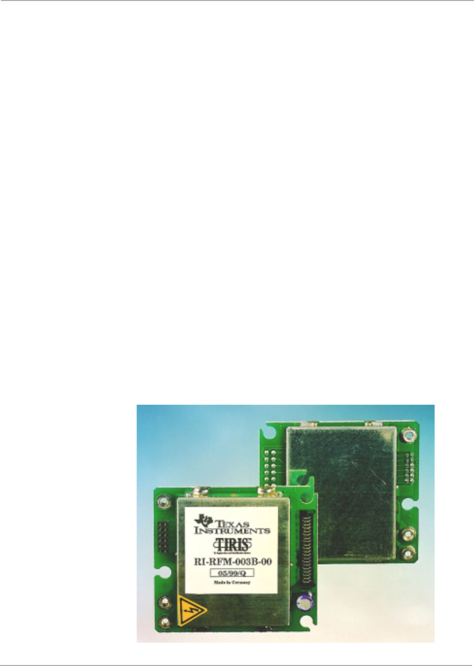
1.3 Product Description
The Mini-Radio Frequency Module is an integral part of a TIRIS system, together
with a control module or unit and an antenna it is used for wireless identification of
TIRIS transponders.
Main tasks of the RF module are to send an energizing signal via the antenna to ini-
tialize a TIRIS transponder, to demodulate the received transponder identification
signal and to write to a transponder. The RF module delivers a digital data stream
and a clock signal for further processing to its control unit or module. Furthermore a
field strength dependent digital output is available for synchronization purposes.
Figure 1: The RI-RFM-003B

7
November ’00 Chapter 1. Introduction
Its small size and low supply voltage makes the Mini-RFM well suited for portable
Reading/Writing Units, as well as for stationary equipment where medium read/write
range and speed is sufficient.
The data input and output lines are compatible with the HCMOS- logic family.
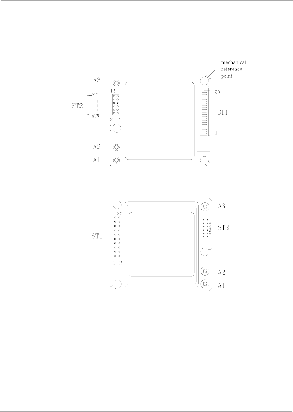
1.4 Mechanical Construction
The RF module has a simple mechanical construction where all the components are
mounted on the Printed Circuit Board (PCB). The components of the upper and lower
side of the PCB are protected by metal shields. The PCB also carries the connectors
ST1, ST2 and the antenna terminals A1 to A3 which are captive nuts soldered to the
PCB. These captive nuts allow durable low resistance connection with the ring ter-
minals of the antenna.

CHAPTER 2
8
Electrical Description
Chapter 2: Functional Description
This chapter provides an electrical description to block diagram level of how the Mini-
RFM works.
Topic Page
2.1 General..........................................................................................................9
2.2 Transmitter ...................................................................................................9
2.3 Receiver ......................................................................................................11
2.4 Antenna Circuit ..........................................................................................11
9
November ’00 Chapter 2. Electrical Description
2.1 General
The RF module is the interface between the TIRIS transponder and the data pro-
cessing unit of a TIRIS Reader. It contains circuitry to:
- send a charge-up signal to a TIRIS transponder
- program a read/write transponder
- to receive the signal from the transponder and to prepare the received signal
for digital decoding.
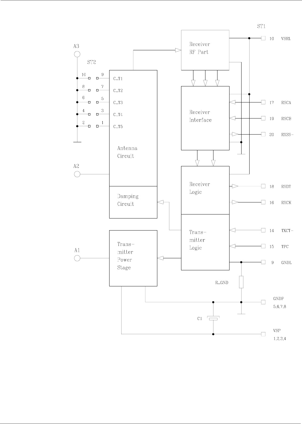
Figure 2 shows the block diagram of the RF module and unless otherwise noted the
following description refers to this schematic.
2.2 Transmitter
The transmitter control logic generates the transmitter output frequency from a
crystal-controlled oscillator. This signal is amplified by the push-pull transmitter
power stage which is connected to the antenna terminal A1. The supply current
I_VSP of the transmitter output stage depends on the quality factor of the antenna
being used and the supply voltage VSP. The Mini-RFM’s antenna circuit is shown in
Figure 3.
The transmitter control signal TXCT- activates the transmitter as long as it is “low”.
In receive mode when TXCT- is “high” the antenna terminal A1 has a low impedance
path to the ground.
The transmitter power control signal TPC controls the intensity of the transmitter
charge pulse by changing the duty cycle of the power stage control signal. The level
of the RF power output can be reduced by setting the TPC signal to “low”. TPC con-
trols the power setting of the RF signal which is used to make-up the “power-burst”.
Both input signals TXCT- and TPC have internal pull-up resistors.
Because of the limited heatsink possibilities of the transmitter power transistors the
duty cycle of the power pulse must not be allowed to exceed that shown in Figure 6.
CAUTION:
Because of the necessarily low impedance of the output
stage, a short-circuit from antenna terminal A1 either to the
ground or to the supply voltage can damage the output
stage if the supply current is not limited.
10
Mini-RFM - Reference Guide November ’00
Figure 2: Mini-RFM Block Diagram

11
November ’00 Chapter 2. Electrical Description
2.3 Receiver
The receiver comprises three parts: the RF part, the interface and the logic.
The selective amplifier in the RF Part of the receiver:
- amplifies the RF signal received from the antenna circuit, then
- demodulates the FSK signal from the TIRIS transponder, and
- generates an analog voltage (RSSI) that provides an indication of the received
signal strength.
The demodulated FSK signal, carrier signal and analog signal strength voltage are
all connected to the receiver interface. The demodulated data signal and the carrier
signal are converted to logic signals, and connected to the receiver logic for further
processing. The signal strength indicator voltage is converted into RXSS- which is
fed directly to the module connector ST1. The function of the RXSS- signal is ex-
plained in more detail in section 5.3.
The receiver logic generates the receiver data signal RXDT and the receiver clock
signal RXCK to allow a simple data processing. The NRZ data stream of RXDT con-
tains the identification data, the protection data and the framing bits. The clock signal
RXCK is used as time reference for the data stream of RXDT. The RXCK signal
changes from “low” to “high” level in the middle of each data bit.
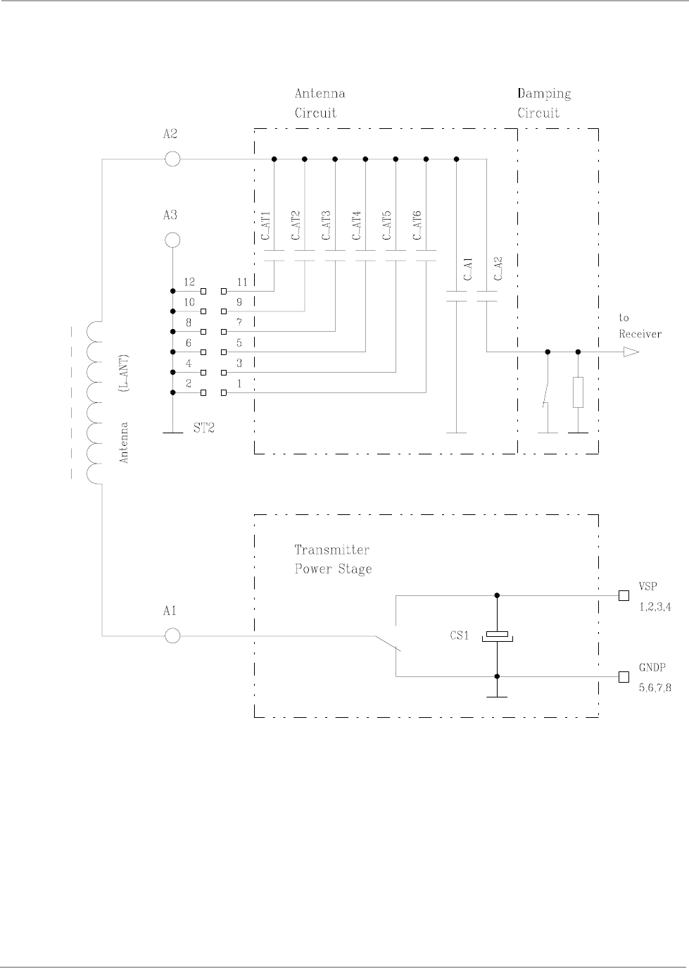
2.4 Antenna Circuit
Figure 3 shows a simplified schematic of the antenna circuit. The antenna coil L_ANT
is not part of the module but together with the antenna circuit’s built-in capacitors it
forms a resonance circuit. The resonant current through the antenna coil generates
the magnetic field which charges (and programs) the transponder.
For the system to transmit and receive correctly, the antenna must be precisely tuned
to the transmitter output frequency f_TXO to compensate for the (allowed) tolerances
of the antenna coil L_Ant and the antenna capacitors C_A1 and C_A2. To enable this
tuning, six tuning capacitors C_AT1 to C_AT6 have been added to the antenna cir-
cuit. Their values are binary weighted in normalized steps of 1, 2, 4, 8 16 and 32.
C_AT1 has the smallest value corresponding to the normalized value 1. C_AT2 has
the double capacitance of C_AT1, so that C_AT2 corresponds to the normalized val-
ue 2 and so on. With this capacitance array and six jumpers, 64 different capacitance
values can be tuned. Each of the five tuning pins has its adjacent antenna ground pin
for a simple short circuit with jumpers.
The antenna terminal A3, which is not used in normal applications and the antenna
ground pins of ST2 have same potential as GNDP but should be used only for an-
tenna purposes and not as a convenient ground connection.
The damping circuit is part of the antenna circuit and damps the antenna circuit by
reducing the quality factor of the built-in antenna circuit capacitor connected to the
terminal A2. The quality factor is reduced during the receive mode when the TXCT-
signal is “high”.
Information about the tuning of the antenna circuit is given in section 5.6.
12
Mini-RFM - Reference Guide November ’00
Figure 3: Mini-RFM’s Antenna Circuit

CHAPTER 3
13
Connectors
Chapter 3: Connectors
This chapter contains a listing of the module’s two connectors (ST1 and ST2) togeth-
er with a list of the signals contained on each pin.
Topic Page
3.1 Connector Location ...................................................................................14
3.2 Connector ST1............................................................................................15
3.3 Connector ST2............................................................................................16
3.4 Antenna Connector....................................................................................16
14
Mini-RFM - Reference Guide November ’00
3.1 Connector Location
Figure 4 and Figure 5 show the location of the terminals on the PCB from the top and
from the bottom.
Figure 4: Top View
Figure 5: Bottom View

15
November ’00 Chapter 3. Connectors
3.2 Connector ST1
Table 1: Module Connector - ST1
Pin
Number Signal
Name Purpose
1 VSP Supply Voltage for Power Stage (+)
2 VSP Supply Voltage for Power Stage (+)
3 VSP Supply Voltage for Power Stage (+)
4 VSP Supply Voltage for Power Stage (+)
5 GNDP Ground for Power Stage (-)
6 GNDP Ground for Power Stage (-)
7 GNDP Ground for Power Stage (-)
8 GNDP Ground for Power Stage (-)
9 GNDL Ground for Logic (-)
10 VSRL Regulated Supply voltage for Receiver and Logic (+)
11 N.C. Not connected
12 N.C. Not connected
13 N.C. Not connected
14 TXCT- Transmitter Control Input, inverted
15 TPC Transmitter Power Control Input
16 RXCK Receiver Clock Output
17 RSCA Receiver Synchronization Level Control Input, weighted 1
18 RXDT Receiver Data Output
19 RSCB Receiver Synchronization Level Control Input, weighted 2
20 RXSS- Receiver signal strength output, inverted
Important Note:
Supply terminals GNDP and GNDL must be connected externally.
16
Mini-RFM - Reference Guide November ’00
3.3 Connector ST2
3.4 Antenna Connector
Table 2: Antenna Tuning Connector - ST2
Pin
Number Signal
Name Purpose
1 C_AT6 Antenna Tuning Capacitor 5, (weighted value 32)
2 GNDP Antenna Ground
3 C_AT5 Antenna Tuning Capacitor 5, (weighted value 16)
4 GNDP Antenna Ground
5 C_AT4 Antenna Tuning Capacitor 4, (weighted value 8)
6 GNDP Antenna Ground
7 C_AT3 Antenna Tuning Capacitor 3, (weighted value 4)
8 GNDP Antenna Ground
9 C_AT2 Antenna Tuning Capacitor 2, (weighted value 2)
10 GNDP Antenna Ground
11 C_AT1 Antenna Tuning Capacitor 1, (weighted value 1)
12 GNDP Antenna Ground
Table 3: Antenna Connector
Pin
Number Purpose
A1 Antenna Terminal 1
A2 Antenna Terminal 2
A3 Antenna Ground (GNDP)
CAUTION:
Never try to connect the antenna between A1 and A3, or A2
and A3; as this will damage the module.

CHAPTER 4
17
Specifications
Chapter 4: Specifications
This chapter provides the specific details that you will need in order to use the TIRIS
Mini-Radio Frequency Module RI-RFM-003B correctly. It includes general data, elec-
trical characteristics, timing characteristics and mechanical data.
Topic Page
4.1 Recommended Operating Conditions......................................................18
4.2 Electrical Characteristics ..........................................................................18
4.3 Timing Characteristics ..............................................................................20
4.4 Mechanical Data.........................................................................................21
18
Mini-RFM - Reference Guide November ’00
4.1 Recommended Operating Conditions
Operating free-air temperature range.......................... 0 to +50 °C
Storage temperature range........................................ -25 to +85 °C
4.2 Electrical Characteristics
at Tamb=25 °C, VSRL=5.0V (unless otherwise noted)
Note:
Free-air temperature: air temperature immediately surrounding the
Mini-RFM. If the module is incorporated into a housing, it must be
guaranteed by proper design or cooling that the internal temperature
does not exceed the ratings given here.
Parameter Description Condition Pin No.
of ST1 min. max Unit
VSRL Supply voltage for logic - 10 4.75 5.25 V
VSP Supply voltage for
transmitter power stage - 1,2, 3, 4 4.5 6.0 V
VIL Low level input voltage for
TXCT- and TPC VSRL=5.0 14, 15 0 1.0 V
VIH High level input voltage for
TXCT- and TPC VSRL=5.0 14, 15 4.0 5.0 V
Note:
The voltage difference between GNDL and GNDP must not exceed
0.5 V.
Parameter Description Condition Pin No.
of ST1 min. nom. max Unit
I_VSRL Supply current for logic and receiver - 10 - - 80 mA
I_VSP Supply current for transmitter power
stage with antenna Ri-ANT-P02A
VSP=5V
TXCT-=”low”
TPC=”high” 1,2,3,4 0.5 - 1.2 A
I_VSP_L Leakage current for transmitter power
stage with antenna Ri-ANT-P02A VSP=5V
TXCT-=”high” 1,2,3,4 - - 50 µA
R_up Pull-up resistor from TXCT- and TPC
to VRSL ---22-kOhm
I_IL Low level input current for TCXT- and
TPC V_IL=0V 14, 15 -180 - -300 µA
I_IH High level input current for TCXT-
and TPC V_IL=4V 14, 15 -30 - -60 µA
19
November ’00 Chapter 4. Specifications
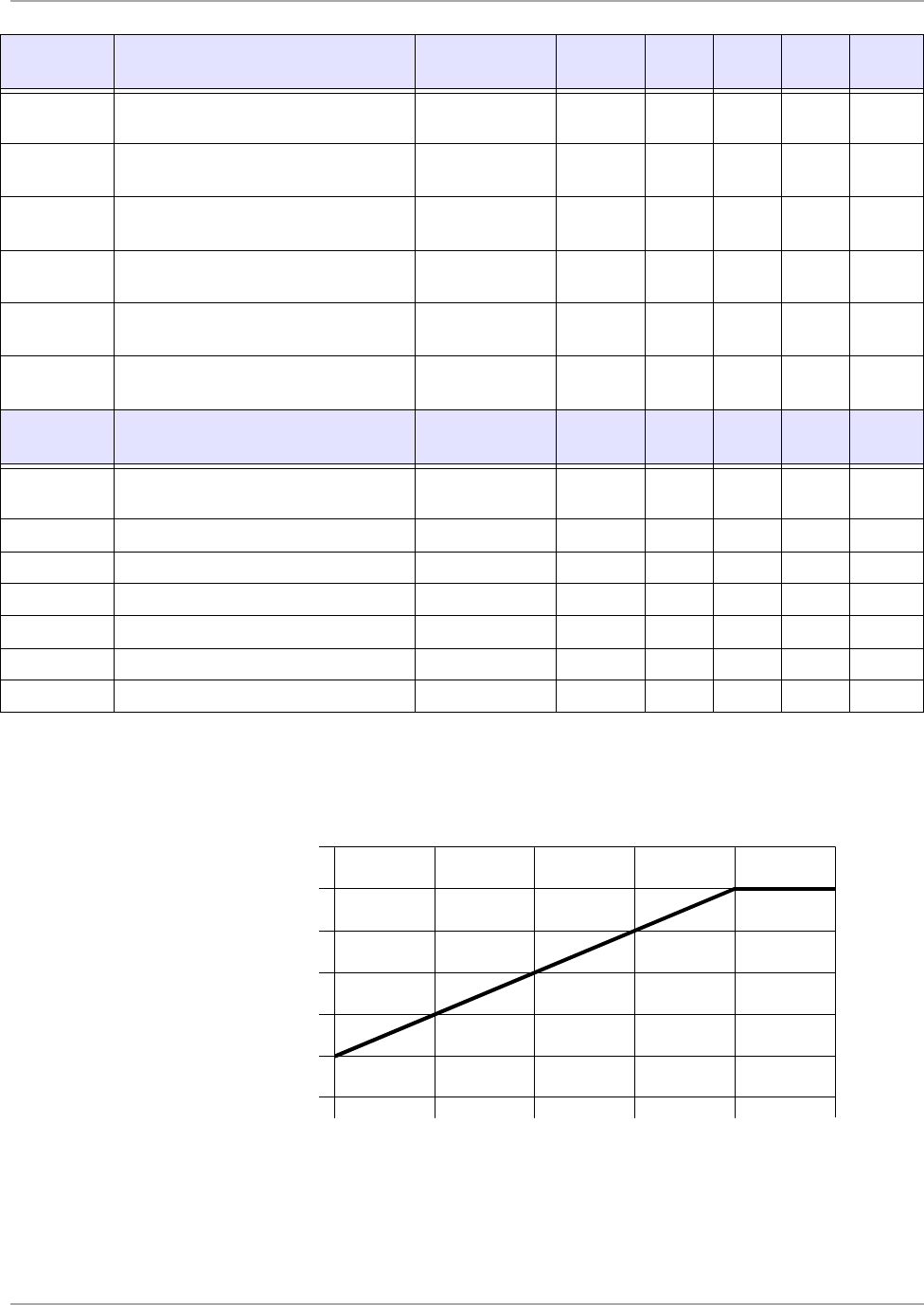
Figure 6: Maximum Supply Current I_VSP versus t_off (Power Stage)
Time t_off between 2 charge pulses of 50 ms [ms]
Values in brackets ( ) are for time t_off between 2 write cycles
I_IL Low level input current for RSCA and
RSCB V_IL=0V 17, 19 - -30 µA
I_IH High level input current for RSCA and
RSCB V_IH=5V 17, 19 - - 30 µA
V_OH High level output voltage for RXCK,
RXDT and RXSS- I_OH=-2mA 16, 18,
20 2,4--V
V_OH High level output voltage for RXCK,
RXDT and RXSS- I_OH=-1mA 16, 18,
20 4.0--V
V_OL Low level output voltage for RXCK,
RXDT and RXSS- I_OL=-2mA 16, 18,
20 --0.5V
R_GND Decoupling resistor between GNDL
and GNDP -9 to
5,6,7,8 -33-Ohm
Parameter Description Condition Pin No.
of ST2 min. nom. max Unit
C_A1
+C_A2 Antenna capacity without tuning
cap. A2 10.6 - 11.8 nF
C_AT6 Antenna tuning capacity weighted 32 - 1 1425 1500 1575 pF
C_AT5 Antenna tuning capacity weighted 16 - 3 740 780 820 pF
C_AT4 Antenna tuning capacity weighted 8 - 5 370 391 410 pF
C_AT3 Antenna tuning capacity weighted 4 - 7 209 220 231 pF
C_AT2 Antenna tuning capacity weighted 2 - 9 95 100 105 pF
C_AT1 Antenna tuning capacity weighted 1 - 11 50 56 64 pF
Parameter Description Condition Pin No.
of ST1 min. nom. max Unit
1.8
1.5
1.2
0.9
0.6
0.3
0
50
(250) 100
(400) 150
(550) 200
(700) 250
(850)
0
I_VSP_max [A]

20
Mini-RFM - Reference Guide November ’00
4.3 Timing Characteristics
at Tamb=0-50 °C, VSRL=5.0 V, VSP=5.0 V
Parameter Description Condition Pin No.
of ST1 min. nom. max. Unit
f_TX Transmitter frequency - A1 134.1 134.2 134.3 kHz
f_OSC Internal oscillator
frequency - - - 4294.4 - kHz
f_mRX Center frequency of
receiver - - - 128.2 - kHz
b_RX Bandwidth of receiver - - - 22 - kHz
t_rin,
t_fin
Rise and fall time of
the input signals
TXCT- and TPC - 14, 15 - - 100 ns
t_rout,
t_fout
Rise and fall time of
the output signals
RXCK, RXDT, RXSS- -17, 18,
20 --1µs
f_REPwrt Repetition rate to
program with Antenna
= RI-ANT-P02A
t_wrt=310ms
TPC=”high ---1Hz
f_REPrd Repetition rate to read
with Antenna =
RI-ANT-P02A
t_charge=
50ms
TPC=”high” ---4Hz
t_offL Transmitter OFF-time
for databit = “L” t_bit=2ms - - 0.5 - ms
t_offH Transmitter OFF-time
for databit=”H” t_bit=2ms - - 1.2 - ms
21
November ’00 Chapter 4. Specifications
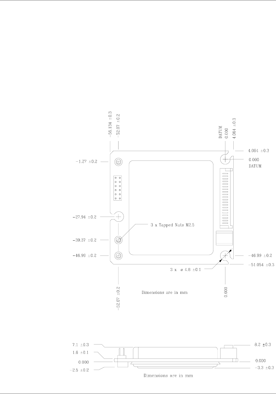
4.4 Mechanical Data
Length......................................................................... 60.2 mm
Width........................................................................... 55.1 mm
Height, body................................................................ 10.4 mm
Height, at connector.................................................... 11.5 mm
Weight......................................................................... 40 g
Figure 7 shows the top view and Figure 8 shows the side view of the RF module, both
drawings show the most important dimensions. The center of the upper right mount-
ing hole serves as reference point for all dimensions.
Figure 7: Mechanical Dimensions - Top View
Figure 8: Mechanical Dimensions - Side View

CHAPTER 5
22
Installation and Use
Chapter 5: Installation and Use
This chapter provides the specific details that you will need in order to install the
TIRIS Mini-RFM correctly. It includes a detailed description of the power supply re-
quirements, the antenna characteristics, the connecting cable and how to tune the
antenna to resonance.
Topic Page
5.1 Mechanical Mounting...............................................................................23
5.2 Supply Voltage .........................................................................................23
5.3 Receiver Signal Strength Output RXSS-................................................25
5.4 Programming a Transponder..................................................................27
5.5 Antenna Requirements............................................................................27
5.6 Antenna Tuning........................................................................................29
5.6.1 To Switch-ON the Transmitter..............................................................29
5.6.2 To Tune the Antenna Circuit ................................................................29
5.6.3 To Detect the Correct Tuning...............................................................29
5.6.4 Tuning Procedure.................................................................................30
23
November ’00 Chapter 5. Installation and Use
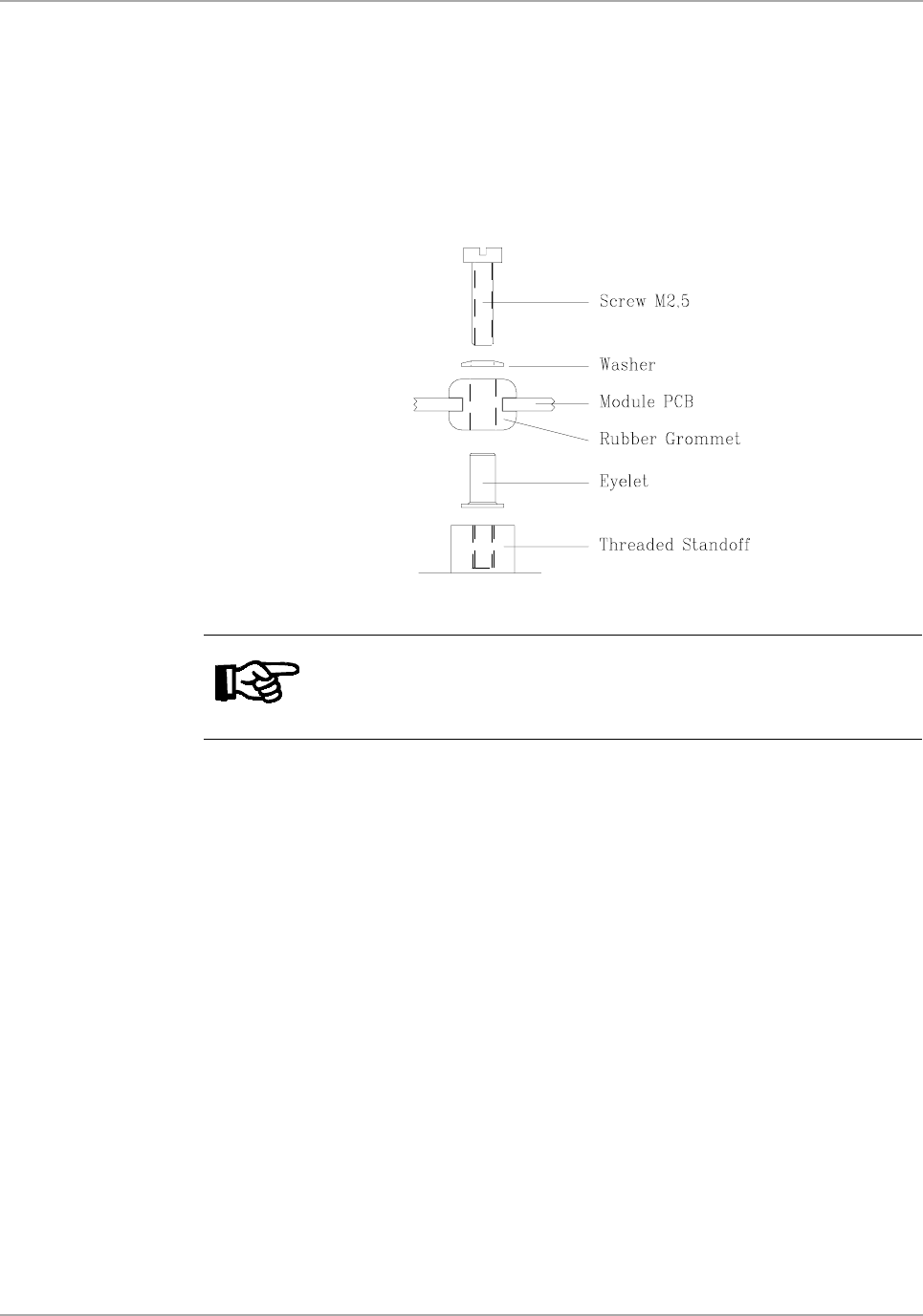
5.1 Mechanical Mounting
To protect the RF module from strong mechanical shock and vibration, grommets are
inserted into the mounting hole of the PCB as shown in Figure 9. Because the grom-
mets are made of soft material, eyelets or spacers must be inserted into them when
the RF module is mounted with screws.
Figure 9: PCB Mounting Proposal
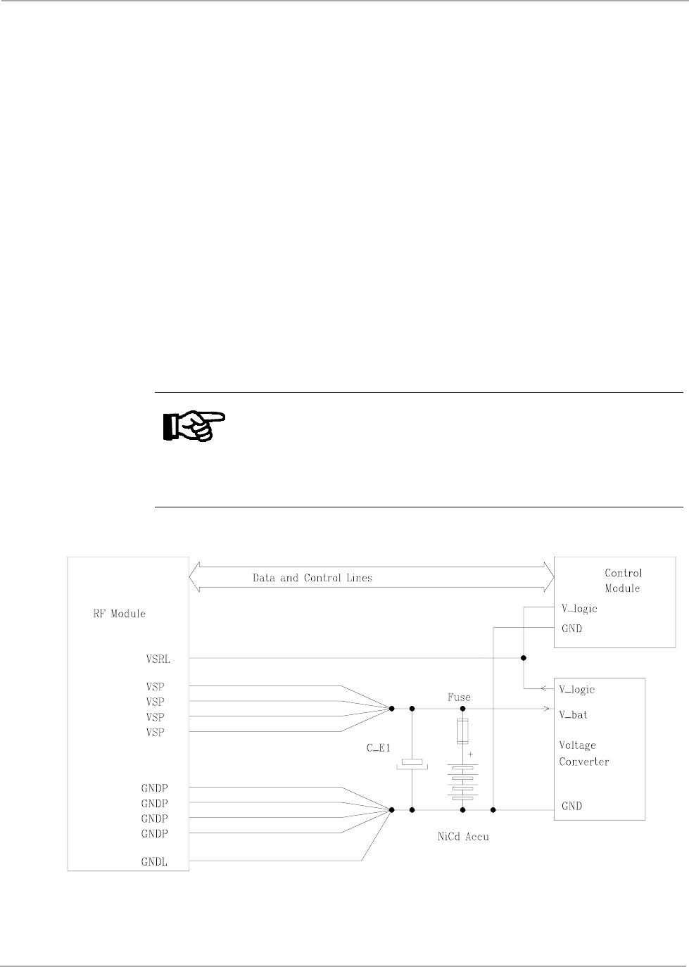
5.2 Supply Voltage
The module uses two different supply lines each with a separate ground line. The re-
ceiver and the logic are supplied via the VSRL and GNDL pins from a voltage regu-
lated power supply. The transmitter power stage with its relatively high current
consumption is supplied via the VSP and GNDP pins. The supply voltage range for
VSP is wider than for VSL. This allows the direct connection of VSP to a four cell
NiCd battery, if the variation of the power pulse field strength caused by the variation
of the battery voltage is acceptable.
Both ground lines GNDL and GNDP are decoupled inside the RFM with the resistor
R_GND and the capacitor C_GND and have to be connected together externally as
shown in Figure 10 or Figure 11 (depending on your power supply). This technique
allows the power ground level GNDP to float in a certain range against the logic
ground level GNDL without creating adverse effects to the control signals from and
to the control unit. Floating GNDP can happen during transmit time if you are using
a long supply line between the RF module and a control module.
Note:
Take care when disconnecting ST1 that you pull the plug straight out
and do not apply any sideways strain to the plastic guides.
24
Mini-RFM - Reference Guide November ’00
Figure 10 shows an example of how to supply the RF module in a battery supplied
reading unit where short lines are possible.
Figure 11 shows an example of how to wire a stationary application where long sup-
ply lines (over 15 cm) are used. The capacitor C_E1 between the VSP and GNDP
pins is necessary to reduce the RF ripple voltage and EMI on the supply line and
must have low impedance at the transmit frequency (ESR = Equivalent Serial Resis-
tor). In addition the common mode choke coil (choke) and the capacitor C_E2 also
reduce the EMI during transmit time. These components should be placed as closely
as possible to the RF module connector ST1.
The capacitor values shown in Figure 10 and Figure 11 are for general use and can
vary according to different application requirements.
Regardless of which kind of power supply you use, we recommend that you build in
fuses or electronic current limitations in between the RF module and the power sup-
plies to avoid any damage in case of short circuit. The value of the fuse depends very
much on the application, for example: the current consumption of the module which
in turn depends on several factors, such as: the antenna used, whether or not a ca-
pacitor is connected and its size.
Figure 10: Supply Line Wiring for Short Supply Lines
Note:
The fuse load for VSP under normal conditions is less than 1 A.
However, if the Mini-RFM is connected into an application where the
power is permanently on (hot” connecting), the load could surge by
several amps due to the current in capacitor CS1 inside the Mini-
RFM.
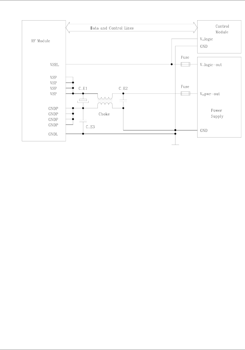
25
November ’00 Chapter 5. Installation and Use
Figure 11: Supply Line Wiring for a Separated Power Supply
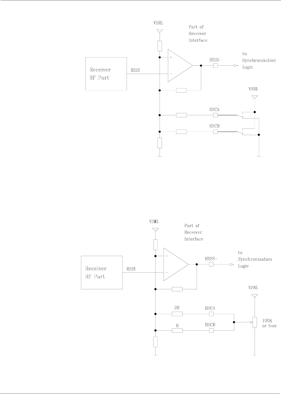
5.3 Receiver Signal Strength Output RXSS-
If you are going to operate more than one TIRIS reader in a local area, the systems
should be synchronized to each other. An intelligent control unit achieves this syn-
chronization by sampling for the presence or absence of the field strength indicator
signal RXSS-. A power pulse in the area will cause RXSS- to be active. If the signal
RXSS- is present the control unit ensures that the RF module transmits either simul-
taneously or sequentially to any other RFMs in the area.
The RXSS- output switches to “low” if the received signal strength exceeds the inter-
nal reference level. This reference level can be adjusted with the two receiver signal
strength control inputs RSCA and RSCB.
Figure 12 and Figure 13 show the basic schematic of the signal strength indicator
and two methods of adjusting the switching level.
The circuit shown in Figure 12 works as a simple D/A converter where the digital in-
puts RSCA and RSCB are switched either to the ground GNDL or to the supply volt-
age VSRL. Because of the high input impedance of RSCA and RSCB, the switches
can be replaced by computer controlled outputs. Such a circuit can adjust the sensi-
tivities in four steps. A fifth step is given if both inputs are open.
26
Mini-RFM - Reference Guide November ’00
Figure 12: Synchronization output Control - Digital Adjustment
An analog adjustment of the sensitivity level can be realized if a potentiometer is
used as shown in Figure 13 or if a variable voltage source is used to bias one or both
of the control inputs RSCA and RSCB.
Figure 13: Synchronization output Control - Analog Adjustment
27
November ’00 Chapter 5. Installation and Use
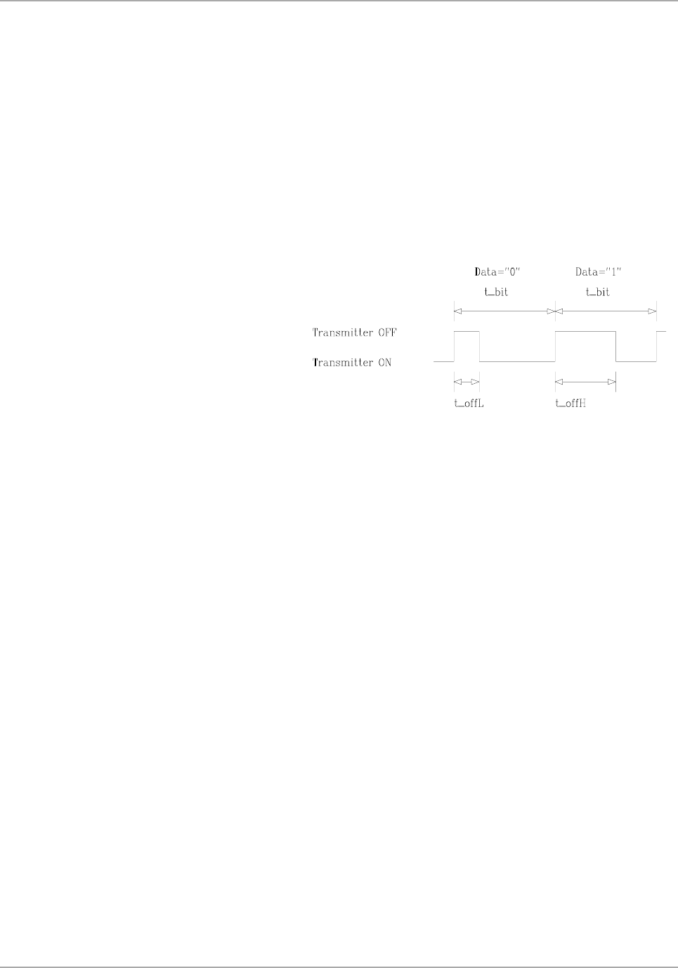
5.4 Programming a Transponder
To write data to a read/write transponder the transmitter of the RF module must be
switched off and on periodically after the power pulse is completed. As shown in Fig-
ure 14 each data bit has the same length t_bit, but the duration t_offL or t_offH during
which the transmitter is switched off, determines the value of the bit. Because the an-
tenna circuit of the module and the connected antenna form a resonance circuit with
a specific rise and fall characteristic of the resonance voltage, different RF module
and antenna combinations might need different t_offL and t_offH timing. The values
t_offL and t_offH shown in section 4.3 'Timing Characteristics' are the times applied
to TXCT-. A high Q antenna such as RI-ANT-P02A is used.
Figure 14: Write Pulse Timing for TXCT-
A detailed description of the complete programming sequence is given in the Se-
quence Control Manual (document number 11-06-21-049).
5.5 Antenna Requirements
The antenna for a TIRIS RF module is a coil with the inductance L_ANT and the Q-
factor Q_ANT. To ensure that the antenna can be tuned to resonance with the tuning
capacitors inside the RF Module, the inductance L_ANT for an air coil antenna can
vary in the limits given below:
L_ANT = 115 to 117 µH (at f=134.2 kHz, V=1V)
Q_ANT = 200 or better is recommended for good read/write range.
Some factors which often influence each other, are listed below.
a. The size and the construction of the antenna coil is a key factor for the generated
magnetic field strength. The larger the area of an air coil antenna or the longer a
ferrite core antenna is, the higher the field strength for a given RFM set-up and a
given Q-factor of the antenna coil.
b. The quality factor of the antenna coil is a parameter indicating its efficiency. The
quality depends on the construction and the wire used for the coil. Because of the
high frequency, litze-wire is needed for a high Q-factor. The higher the Q-factor of
the antenna coil the more energy can be “pulled” from the RF module for a given
RF module set-up. If an antenna with ferrite core is used, it must be kept in mind
that it may have a very high quality factor under test conditions, but the quality
factor will drop if a high magnetic field is applied to the ferrite core.
c. A very important factor for a good read/write range is the correct orientation /
polarization between the transponder antenna and the antenna of the read/write
unit.
28
Mini-RFM - Reference Guide November ’00
d. Noise, i.e. magnetic interference energy in or close to the TIRIS frequency range
can reduce the read range remarkably. Sources of interference can be, for
example: electronic equipment with built-in switch mode power supplies, monitors
and TV-sets with their magnetic deflection, which are not shielded enough. In such
conditions you may be able to obtain better read/write ranges with a smaller
antenna rather than a large one. The reason for this is that a large antenna collects
signals within a larger area and therefore produces a stronger interference signal
compared with the relatively small transponder signal. Under some conditions,
charging and/or writing to the transponder works excellently, but the reading unit
cannot detect the transponder signal.
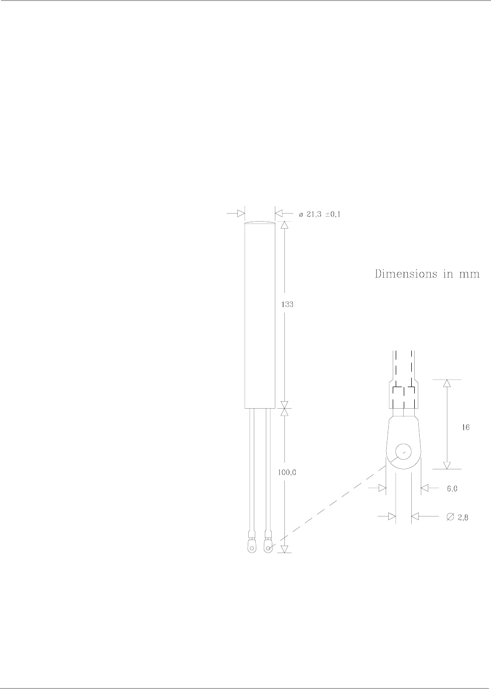
Figure 15 shows the dimensions of the ferrite stick antenna RI-ANT-P02A available
for the RF Module RI-RFM-003B.
Figure 15: Stick Antenna RI-ANT-P02A

29
November ’00 Chapter 5. Installation and Use
5.6 Antenna Tuning
In order to get all the available field strength from the antenna, it must be tuned to
resonance. To do this, the following set-up and equipment are required.
5.6.1 To Switch-ON the Transmitter
The reading/writing unit or test set up should be able to switch the RF module’s trans-
mitter to a fast repeating reading mode or continuous wave mode. If a continuous
wave mode is applied, care must be taken not to exceed the duty cycle limitation as
given in section 4.3. Time when the transmitter is switched on but during which the
current consumption is less than I_VSPcont, does not add to the duty cycle.
5.6.2 To Tune the Antenna Circuit
The built-in tuning capacitors C_AT1 to C_AT6 which are available at ST2 should be
used to tune the resonance frequency of the antenna circuit to the output frequency
of the transmitter. The most simple method of tuning is to use a “Switch Box” con-
nected to the antenna tuning connector ST2, this will allow the capacity of the anten-
na resonant circuit to be increased by connecting the built-in tuning capacitors to the
ground.
The “Switch Box” in its simplest version is an array of six well isolated, high voltage
proof ON/OFF switches, which are connected to the antenna tuning connector ST2
(Antenna Tuning Switch Box RI-ACC-ATS1).
If you have to tune a lot of Mini-RFMs (for example on a production run) it would be
helpful to build a computer (or electronically) controlled tuning box which allows you
to start the tuning procedure and then set the jumpers according to the result of the
tuning. The cable from the “switch box” to the connector ST2 should be as short as
possible (less that 20 cm) in order to get the same tuning results as with the jumpers.
5.6.3 To Detect the Correct Tuning
There are two basic methods to detect the correct tuning point, they are:
One method is to tune the antenna circuit to maximum current consumption of
the transmitter power stage by inserting a current meter into the VSP-line
which is an easy way for production. The lines of the meter should be as short
as possible, or they must be RF decoupled close to the RF module.
The second method is to tune the antenna circuit to the maximum of the mag-
netic field strength generated by the antenna.
30
Mini-RFM - Reference Guide November ’00
5.6.4 Tuning Procedure
Ensure that the reader is switched OFF.
Connect the antenna to the RF Module.
Remove all jumpers from the tuning connector ST2 and connect the “Switch Box”
with all six switches in the OFF position.
Switch the RF module transmitter ON (continuous or fast reading mode).
While watching the current meter, increase tuning capacity with the “Switch Box”
step-by-step until you find a peak.
When you find a peak continue with two more steps and check in case you find an-
other, higher peak. Looking for a possible second peak is necessary because the ca-
pacitors of the tuning network have overlapping capacitance, which causes
discontinuous capacitance steps.
Check if the power stage supply current or the field strength has the correct value for
that application.
Switch the transmitter OFF, disconnect the switch box and then plug-in jumpers at
all the places where the switches are in the ON position.
Switch ON the equipment again and check if the current or field strength are almost
the same as they were with the switch box connected.
Switch OFF the transmitter or reading unit. Tuning is completed.
WARNING:
CARE MUST BE TAKEN WHEN HANDLING THE M
INI-RFM. HIGH
VOLTAGE ACROSS THE ANTENNA TERMINALS AND TUNING CONNEC-
TORS COULD BE HARMFUL TO YOUR HEALTH. IF THE ANTENNA
INSULATION IS DAMAGED IT MUST NOT BE CONNECTED TO THE
MINI-RFM.
Note:
If you are using a switch box, do not forget that the capacitors
attached to the jumpers are binary weighted, and that you should set
the switches in a binary way:
Switch 1 ON
Switch 1 OFF Switch 2 ON
Switch 1 ON Switch 2 ON
Switch 1 OFF Switch 2 OFF Switch 3 ON
and so on.

CHAPTER 6
31
Warnings, Cautions and Notices
Chapter 6: Warnings, Cautions and Notices
This chapter provides the Warnings, Cautions and Notices that are relevant to the
Mini-RFM.
Topic Page
6.1 FCC / Telecommunications Regulations .................................................32
6.2 Important Note to Purchasers/Users of the Mini-RFM in the USA ........32
6.3 Warning.......................................................................................................32
6.4 Cautions......................................................................................................32

32
Mini-RFM - Reference Guide November ’00
6.1 FCC / Telecommunications Regulations
The TIRIS RF Module generates RF emissions at 134.2 kHz. The radiation of the
fundamental and the harmonics will vary with the type of antenna and other devices
or functions connected to the RF module.
The required FCC or Telecommunications approvals must be obtained prior to oper-
ating the TIRIS RF Module with antenna(s), power supply and a control module or
other devices.
Sale, lease or operation in other countries may be subject to prior approval by the
government or other organizations.
6.2 Important Note to Purchasers/Users of the Mini-RFM in the USA
The TIRIS RF Module product is considered by the Federal Communications Com-
mission (FCC) to be a “subassembly”. As such, no prior approval is required to im-
port, sell or otherwise market the RF Module in the United States. In order to form a
functioning radio frequency RF device, the RF Module must be connected to a suit-
able antenna, power supply, and control circuitry. A radio frequency device may not
be operated unless authorized by the FCC nor may a radio frequency device be mar-
keted (i.e. sold, leased, imported, or advertised for sale or lease) without the prior
grant of an FCC equipment authorization.
FCC authorization to operate an RF device may take one of two forms: first, the FCC
may grant the user an experimental license; second, the FCC may issue an equip-
ment authorization permitting use of the RF device on an unlicensed basis. TI can
assist the user in obtaining an experimental license that will cover a specific installa-
tion of the RF Module in a specific site or sites. Experimental authorizations are ap-
propriate to cover operations during the development of an RF device. A grant of
equipment authorization (known as “certification”) must be obtained from the FCC
before RF devices are marketed or operated on a nondevelopment basis.
An equipment authorization has already been issued for use of the RF Module and
other TIRIS equipment (including antennas) in certain configurations. This authoriza-
tion does not cover all possible combinations of equipment and, in particular, covers
only specific antenna configurations. Should a user desire to use the RF Module in
a configuration not yet approved, TI can assist that customer to obtain the necessary
equipment approval.
6.3 Warning
Care must be taken when handling the RF Module. High voltage across the antenna
terminals and tuning connector could be harmful to your health. If the antenna insu-
lation is damaged it should not be connected to the RF Module.
6.4 Cautions
The RF Module might be subject to damage by electrostatic discharge (ESD) and
should therefore only be handled by ESD protected personnel at ESD secured work-
places.

33
November ’00 Chapter 6. Warnings, Cautions and Abbreviations
The transmitter power output stage can be damaged, if the antenna terminal A1 has
a short circuit either to the ground or to the supply voltage and no current limitation
is applied.
The transmitter power output stage can operate only with a limited duty cycle. This
subject needs to be given attention especially during the antenna tuning procedure.
The ground pins GNDL and GNDP have to be connected externally to avoid damage
to the RF Module.

34
Mini-RFM - Reference Guide November ’00