Texas Pci445X Users Manual PC Card And 1394 OHCI Link Controller Implementation Guide
Texas-Instruments-Pci445X-Users-Manual-400209 texas-instruments-pci445x-users-manual-400209
PCI445X to the manual 5512d998-0a69-482b-90e9-a98ea45270d5
2015-02-04
: Texas Texas-Pci445X-Users-Manual-390411 texas-pci445x-users-manual-390411 texas pdf
Open the PDF directly: View PDF ![]() .
.
Page Count: 46

August 2000 PCI Bus Solutions
Implementation
Guide
SCPU007
IMPORTANT NOTICE
Texas Instruments and its subsidiaries (TI) reserve the right to make changes to their products or to discontinue
any product or service without notice, and advise customers to obtain the latest version of relevant information
to verify, before placing orders, that information being relied on is current and complete. All products are sold
subject to the terms and conditions of sale supplied at the time of order acknowledgment, including those
pertaining to warranty, patent infringement, and limitation of liability.
TI warrants performance of its semiconductor products to the specifications applicable at the time of sale in
accordance with TI’s standard warranty. Testing and other quality control techniques are utilized to the extent
TI deems necessary to support this warranty. Specific testing of all parameters of each device is not necessarily
performed, except those mandated by government requirements.
Customers are responsible for their applications using TI components.
In order to minimize risks associated with the customer’s applications, adequate design and operating
safeguards must be provided by the customer to minimize inherent or procedural hazards.
TI assumes no liability for applications assistance or customer product design. TI does not warrant or represent
that any license, either express or implied, is granted under any patent right, copyright, mask work right, or other
intellectual property right of TI covering or relating to any combination, machine, or process in which such
semiconductor products or services might be or are used. TI’s publication of information regarding any third
party’s products or services does not constitute TI’s approval, warranty or endorsement thereof.
Copyright 2000, Texas Instruments Incorporated

Notational Conventions
iii
Preface
Read This First
About This Manual
This manual is intended to assist the designer who is attempting to implement
a solution using the PCI4450 or PCI4451. Much, but not all, of the information
contained herein can also be found elsewhere. However, the smaller size of
this manual, as well as its organization by topics of primary interest to the
hardware designer, make it a much more usable source regarding those
problems most likely to be encountered in the design process.
How to Use This Manual
This document contains the following chapters:
Chapter 1,
PCI445X Device
, provides the designer with information and
examples beyond that contained in the data manuals, which will be useful for
implementing solutions using the PCI4450 or PCI4451.
Appendix A,
Global Reset Only Bits, PME Context Bits
contains tabular listings
of those register bits that can only be cleared by a global reset, and of those
register bits used in conjunction with power management events.
Appendix B,
PME and RI Behavior
, provides truth tables that explain events
and conditions which can wake up a device that has been placed in partially
functional state for power conservation.
Appendix C,
PCI445X Buffer Types
, lists the type of signal buffering used for
input and/or output on each terminal of the device.
Notational Conventions
This document uses the following conventions.
Program listings, program examples, and interactive displays are shown
in a special typeface similar to a typewriter’s. Examples use a bold
version of the special typeface for emphasis; interactive displays use a
bold version of the special typeface to distinguish commands that you

Contents
iv
enter from items that the system displays (such as prompts, command
output, error messages, etc.).
Here is a sample program listing:
0011 0005 0001 .field 1, 2
0012 0005 0003 .field 3, 4
0013 0005 0006 .field 6, 3
0014 0006 .even
Here is an example of a system prompt and a command that you might
enter:
C: csr –a /user/ti/simuboard/utilities
In syntax descriptions, the instruction, command, or directive is in a bold
typeface font and parameters are in an
italic typeface
. Portions of a syntax
that are in bold should be entered as shown; portions of a syntax that are
in
italics
describe the type of information that should be entered. Here is
an example of a directive syntax:
.asect “
section name
”,
address
.asect is the directive. This directive has two parameters, indicated by
section name
and
address
. When you use .asect, the first parameter must
be an actual section name, enclosed in double quotes; the second
parameter must be an address.
Square brackets ( [ and ] ) identify an optional parameter. If you use an
optional parameter, you specify the information within the brackets; you
don’t enter the brackets themselves. Here’s an example of an instruction
that has an optional parameter:
LALK
16–bit constant [, shift]
The LALK instruction has two parameters. The first parameter,
16-bit
constant
, is required. The second parameter,
shift
, is optional. As this
syntax shows, if you use the optional second parameter, you must
precede it with a comma.
Square brackets are also used as part of the pathname specification for
VMS pathnames; in this case, the brackets are actually part of the path-
name (they are not optional).
Braces ( { and } ) indicate a list. The symbol | (read as
or
) separates items
within the list. Here’s an example of a list:
{ * | *+ | *– }
This provides three choices: *, *+, or *–.
Unless the list is enclosed in square brackets, you must choose one item
from the list.
Some directives can have a varying number of parameters. For example,
the .byte directive can have up to 100 parameters. The syntax for this
directive is:
.byte
value
1
[, ... , value
n
]

Trademarks
v
This syntax shows that .byte must have at least one value parameter, but
you have the option of supplying additional value parameters, separated
by commas.
Related Documentation From Texas Instruments
PCI4450 GFN/GJG PC Card and OHCI Controller Data Sheet
, SCPS046
PCI4451 GFN/GJG PC Card and OHCI Controller Data Manual
, SCPS054
OHCI.Lynx Configuration Information Application Report
, SLLA077
PHY Layout Recommendations Application Report
, SLLA020A
TSB41LV03A Data Sheet
, SLLS364
http://www.ti.com/sc/1394
http://www.ti.com/sc/docs/apps/analog/1394_physical_layer_controllers.html
FCC Warning
This equipment is intended for use in a laboratory test environment only. It
generates, uses, and can radiate radio frequency energy and has not been
tested for compliance with the limits of computing devices pursuant to subpart
J of part 15 of FCC rules, which are designed to provide reasonable protection
against radio frequency interference. Operation of this equipment in other
environments may cause interference with radio communications, in which
case the user at his own expense will be required to take whatever measures
may be required to correct this interference.
Trademarks
MicroStar BGA is a trademark of Texas Instruments.
TI is a trademark of Texas Instruments.
Windows is a registered trademark of Microsoft Corporation. (Windows 95, Windows)

vi

Contents
vii
Contents
1 PCI445X Device 1–1. . . . . . . . . . . . . . . . . . . . . . . . . . . . . . . . . . . . . . . . . . . . . . . . . . . . . . . . . . . . . . . . .
1.1 System Features Selection 1-3. . . . . . . . . . . . . . . . . . . . . . . . . . . . . . . . . . . . . . . . . . . . . . . . . .
1.1.1 Package Types 1-3. . . . . . . . . . . . . . . . . . . . . . . . . . . . . . . . . . . . . . . . . . . . . . . . . . . . . .
1.1.2 G_RST and PRST 1-3. . . . . . . . . . . . . . . . . . . . . . . . . . . . . . . . . . . . . . . . . . . . . . . . . . .
1.1.3 PME and RI Signaling 1-3. . . . . . . . . . . . . . . . . . . . . . . . . . . . . . . . . . . . . . . . . . . . . . . .
1.1.4 ZV Support 1-3. . . . . . . . . . . . . . . . . . . . . . . . . . . . . . . . . . . . . . . . . . . . . . . . . . . . . . . . .
1.1.5 EEPROM for Subsystem Vendor and Subsystem ID Registers 1-3. . . . . . . . . . . .
1.1.6 PCI and ISA Style Interrupt 1-4. . . . . . . . . . . . . . . . . . . . . . . . . . . . . . . . . . . . . . . . . . .
1.1.7 Socket Power Switches 1-4. . . . . . . . . . . . . . . . . . . . . . . . . . . . . . . . . . . . . . . . . . . . . .
1.1.8 Distributed DMA (DDMA) 1-4. . . . . . . . . . . . . . . . . . . . . . . . . . . . . . . . . . . . . . . . . . . . .
1.1.9 Optional PCI Signals 1-4. . . . . . . . . . . . . . . . . . . . . . . . . . . . . . . . . . . . . . . . . . . . . . . . .
1.1.10 Socket Activity LEDs 1-5. . . . . . . . . . . . . . . . . . . . . . . . . . . . . . . . . . . . . . . . . . . . . . . . .
1.1.11 MFUNC7–MFUNC0 Terminal Assignments 1-5. . . . . . . . . . . . . . . . . . . . . . . . . . . . .
1.1.12 Miscellaneous Functions Description 1-5. . . . . . . . . . . . . . . . . . . . . . . . . . . . . . . . . . .
1.2 System Implementation 1-8. . . . . . . . . . . . . . . . . . . . . . . . . . . . . . . . . . . . . . . . . . . . . . . . . . . . .
1.2.1 Clamping Rails 1-8. . . . . . . . . . . . . . . . . . . . . . . . . . . . . . . . . . . . . . . . . . . . . . . . . . . . . .
1.2.2 PCI Bus Interface 1-8. . . . . . . . . . . . . . . . . . . . . . . . . . . . . . . . . . . . . . . . . . . . . . . . . . . .
1.2.3 PC Card Interface 1-10. . . . . . . . . . . . . . . . . . . . . . . . . . . . . . . . . . . . . . . . . . . . . . . . . .
1.2.4 2-Wire (I2C) Interface for EEPROM 1-10. . . . . . . . . . . . . . . . . . . . . . . . . . . . . . . . . . .
1.3 Sample PCI445X EEPROM Data File 1-12. . . . . . . . . . . . . . . . . . . . . . . . . . . . . . . . . . . . . . . .
1.3.1 P2C Interface for TPS22x6 Power Switch 1-14. . . . . . . . . . . . . . . . . . . . . . . . . . . . . .
1.3.2 Zoomed Video (ZV) Interface 1-14. . . . . . . . . . . . . . . . . . . . . . . . . . . . . . . . . . . . . . . .
1.3.3 Interrupt Signaling Interface 1-15. . . . . . . . . . . . . . . . . . . . . . . . . . . . . . . . . . . . . . . . . .
1.3.4 Miscellaneous Signals 1-15. . . . . . . . . . . . . . . . . . . . . . . . . . . . . . . . . . . . . . . . . . . . . .
1.3.5 Requirement of Pullup/Pulldown Registers 1-16. . . . . . . . . . . . . . . . . . . . . . . . . . . . .
1.4 BIOS Considerations 1-19. . . . . . . . . . . . . . . . . . . . . . . . . . . . . . . . . . . . . . . . . . . . . . . . . . . . . . .
1.4.1 Initialization 1-19. . . . . . . . . . . . . . . . . . . . . . . . . . . . . . . . . . . . . . . . . . . . . . . . . . . . . . . .
1.4.2 System Sleeping State Consideration 1-20. . . . . . . . . . . . . . . . . . . . . . . . . . . . . . . . .
1.4.3 Docking System Consideration 1-21. . . . . . . . . . . . . . . . . . . . . . . . . . . . . . . . . . . . . . .
1.5 Important Information 1-22. . . . . . . . . . . . . . . . . . . . . . . . . . . . . . . . . . . . . . . . . . . . . . . . . . . . . .
1.5.1 G_RST Clamping Rail 1-22. . . . . . . . . . . . . . . . . . . . . . . . . . . . . . . . . . . . . . . . . . . . . . .
1.5.2 PME/RI_OUT Bit Definition 1-22. . . . . . . . . . . . . . . . . . . . . . . . . . . . . . . . . . . . . . . . . .
1.5.3 Serialized IRQ Data Stream 1-22. . . . . . . . . . . . . . . . . . . . . . . . . . . . . . . . . . . . . . . . . .
1.5.4 Socket Power Control 1-22. . . . . . . . . . . . . . . . . . . . . . . . . . . . . . . . . . . . . . . . . . . . . . .
1.5.5 External CLOCK Frequency for P2C Interface 1-22. . . . . . . . . . . . . . . . . . . . . . . . . .

Contents
viii
A Global Reset Only Bits, PME Context Bits A-1. . . . . . . . . . . . . . . . . . . . . . . . . . . . . . . . . . . . . . . . .
A.1 Global Reset Only Bits/PME Context Bits A-2. . . . . . . . . . . . . . . . . . . . . . . . . . . . . . . . . . . . . .
B PME and RI Behavior B-1. . . . . . . . . . . . . . . . . . . . . . . . . . . . . . . . . . . . . . . . . . . . . . . . . . . . . . . . . . . .
B.1 PME and RI Behavior B-2. . . . . . . . . . . . . . . . . . . . . . . . . . . . . . . . . . . . . . . . . . . . . . . . . . . . . . .
C PCI445X Buffer Types C-1. . . . . . . . . . . . . . . . . . . . . . . . . . . . . . . . . . . . . . . . . . . . . . . . . . . . . . . . . . . .
C.1 PCI445X Buffer Types C-2. . . . . . . . . . . . . . . . . . . . . . . . . . . . . . . . . . . . . . . . . . . . . . . . . . . . . . .

Contents
ix
Figures
1–1 Typical System Architecture 1-2. . . . . . . . . . . . . . . . . . . . . . . . . . . . . . . . . . . . . . . . . . . . . . . . . . . .
1–2 Serialized Interrupt Signal 1-5. . . . . . . . . . . . . . . . . . . . . . . . . . . . . . . . . . . . . . . . . . . . . . . . . . . . . .
1–3 EEPROM 2-Wire Interface 1-10. . . . . . . . . . . . . . . . . . . . . . . . . . . . . . . . . . . . . . . . . . . . . . . . . . . .
1–4 TPS22X6 Power Switch Interface 1-14. . . . . . . . . . . . . . . . . . . . . . . . . . . . . . . . . . . . . . . . . . . . . .
1–5 Example of a ZV Interface 1-14. . . . . . . . . . . . . . . . . . . . . . . . . . . . . . . . . . . . . . . . . . . . . . . . . . . . .
1–6 Distributed DMA Signal Connection 1-16. . . . . . . . . . . . . . . . . . . . . . . . . . . . . . . . . . . . . . . . . . . .
1–7 G_RST and VCCP Relationship 1-22. . . . . . . . . . . . . . . . . . . . . . . . . . . . . . . . . . . . . . . . . . . . . . . .

Contents
x
Tables
1–1 Registers and Bits Loadable Through Serial EEPROM 1-11. . . . . . . . . . . . . . . . . . . . . . . . . . . .
1–2 PC Card Interface Pullup Register List 1-16. . . . . . . . . . . . . . . . . . . . . . . . . . . . . . . . . . . . . . . . . .
1–3 PCI Bus Interface Pullup Register List 1-17. . . . . . . . . . . . . . . . . . . . . . . . . . . . . . . . . . . . . . . . . .
1–4 Miscellaneous Terminals Pullup Register List 1-17. . . . . . . . . . . . . . . . . . . . . . . . . . . . . . . . . . . .
1–5 Required Pullup/Pulldown Resistors 1-18. . . . . . . . . . . . . . . . . . . . . . . . . . . . . . . . . . . . . . . . . . . .
A–1 Global Reset Only Cleared Bits A-2. . . . . . . . . . . . . . . . . . . . . . . . . . . . . . . . . . . . . . . . . . . . . . . . .
A–2 PME Context Bits A-3. . . . . . . . . . . . . . . . . . . . . . . . . . . . . . . . . . . . . . . . . . . . . . . . . . . . . . . . . . . . .
B–1 CardBus CTSCHG and Wake-Up Signals Truth Table B-2. . . . . . . . . . . . . . . . . . . . . . . . . . . . . .
B–2 16-Bit Card RI/STSCHG and Wake-Up Signals Truth Table B-2. . . . . . . . . . . . . . . . . . . . . . . . .
C–1 PCI445X Terminal Function Assignment and Buffer Types C-2. . . . . . . . . . . . . . . . . . . . . . . . . .
C–2 Buffer Type Abbreviations C-7. . . . . . . . . . . . . . . . . . . . . . . . . . . . . . . . . . . . . . . . . . . . . . . . . . . . . .

1-1
PCI445X Device
This implementation guide assists platform hardware developers designing
with the PCI445X dual socket PC card and 1394 open host controller interface
(OHCI) link layer controller (LLC). The PCI445X designation refers to any
device in the PCI445X family, for example, the PCI4450 or PCI4451 device.
The document includes an overview of the PCI445X function and features,
terminal assignments and pinout illustrations, PCI445X I/O electrical
characteristics, identification of required passive components and
recommendations for system implementation, and PHY/Link interface signal
isolation considerations.
Advantages of the PCI445X device:
G_RST (Section 1.1.2)
Internal ring oscillator (Section 1.3.1)
Zoomed video auto-detect function (Sections 1.1.4, 1.3.2)
Integrated IEEE1394 OHCI link layer controller
Topic Page
1.1 System Features Selection 1-3. . . . . . . . . . . . . . . . . . . . . . . . . . . . . . . . . . . .
1.2 System Implementation 1-8. . . . . . . . . . . . . . . . . . . . . . . . . . . . . . . . . . . . . . .
1.3 Sample PCI445X EEPROM Data File 1-12. . . . . . . . . . . . . . . . . . . . . . . . . . .
1.4 BIOS Consideration 1-19. . . . . . . . . . . . . . . . . . . . . . . . . . . . . . . . . . . . . . . . . .
1.5 Important Information 1-22. . . . . . . . . . . . . . . . . . . . . . . . . . . . . . . . . . . . . . . .
Chapter 1
1-2
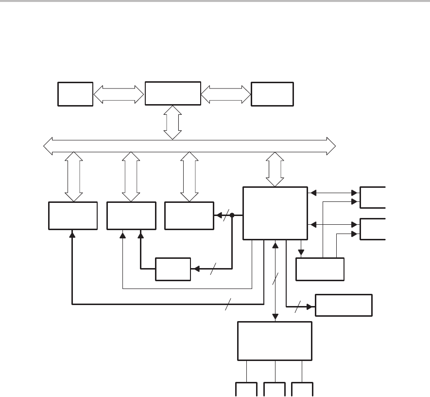
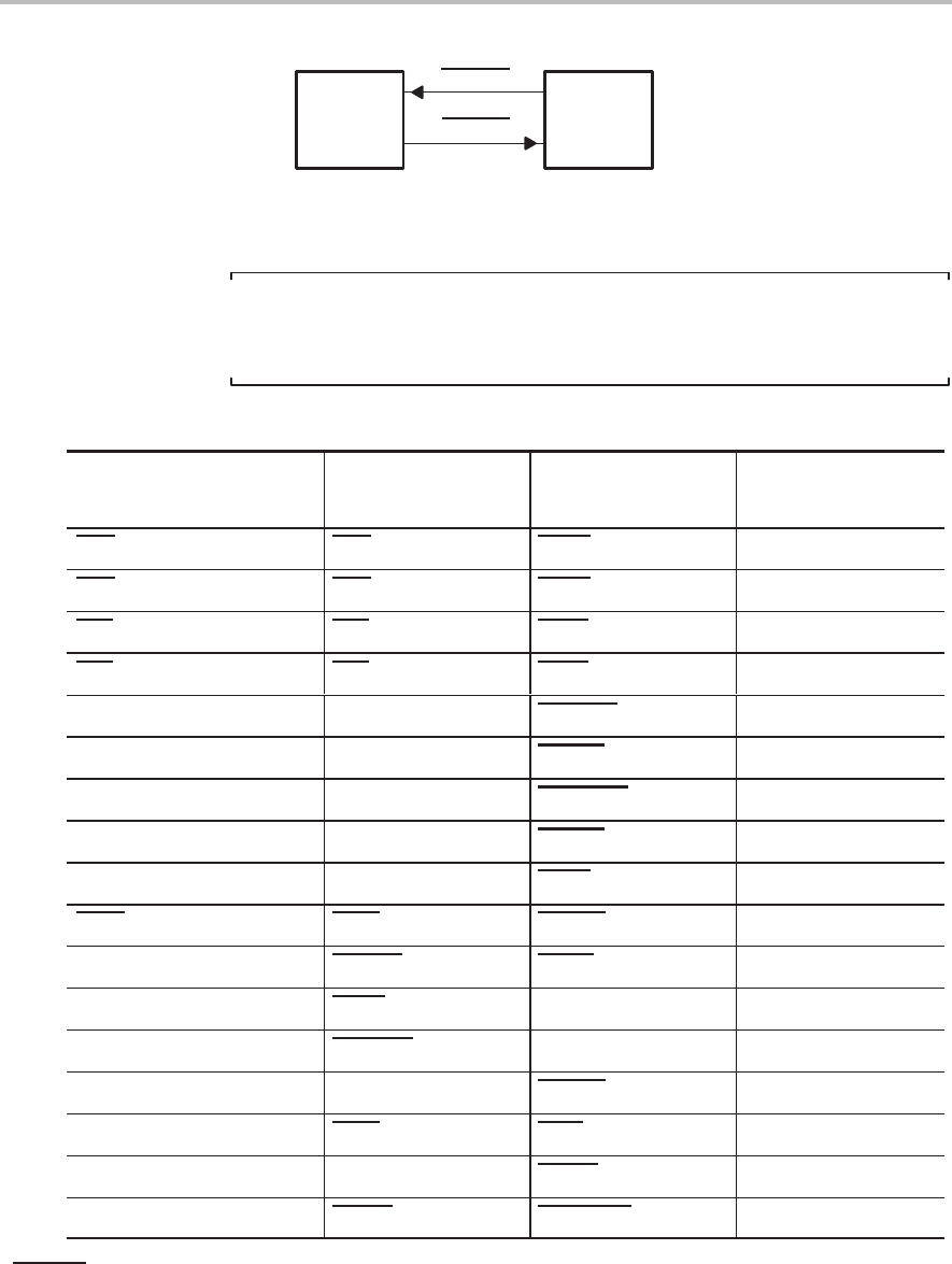
Figure 1–1 illustrates a platform using the PCI445X device along with the
TSB41LV03 3-port PHY, which provides the necessary interface to implement
a 3-port IEEE1394 node.
Figure 1–1. Typical System Architecture
TSB41LV03A
PHY
CPU Memory
North
Bridge
PCI Bus
Graphics
Controller
South
Bridge Sound
Controller
Power
Switch
PC Card
Socket
Power
Interrupt / PME / RI
ZV
2
4
19
EEPROM
Audio
Codec
PCI445X
14

System Features Selection
1-3
PCI445X Device
1.1 System Features Selection
This section explains selectable system features. Feature selection is required
for GPIO and MFUNC terminal assignments and PCI445X register
initialization. Detailed system implementation methods are described in the
following sections. All functions cannot necessarily be used at the same time,
because of the limitations of programmable multifunction terminals (i.e.,
MFUNC7–MFUNC0).
1.1.1 Package Types
The Texas Instruments PCI445X device is offered in two package types:
256-terminal ball grid array (BGA) and 257-terminal MicroStar BGA.
MicroStar BGA is a type of chip scale packaging (CSP).
1.1.2 G_RST and PRST
The PCI445X device has two reset inputs, G_RST and PRST. G_RST resets
all registers and state-machines; PRST resets registers that are not required
to maintain context in a low power state (see Table A–1 and Table A–2). If the
system does not support a wake-up event from D3-state (hot or cold), then
these terminals can be tied together.
1.1.3 PME and RI Signaling
For supporting a wake-up event, a power management event (PME) and/or
an RI signal should be signaled to the system. PME is available only on the
RI_OUT/PME terminal. RI_OUT is available on RI_OUT/PME or MFUNC7.
PME and RI_OUT signals are usually connected to the south bridge or
embedded controller (EC). Detailed PME and RI signal behavior is explained
later.
1.1.4 ZV Support
The PCI445X device has internal zoomed video (ZV) buffers. It can support
three ZV sources, from two PC cards and one external source. Refer to the
detailed implementation guide in Section 1.3.2. The PCI445X device has the
ZV autodetect function for supporting a third external zoomed video source.
ZVSTAT and ZVPCLK are required to support the third source. (The ZV
autodetect function needs ZVPCLK for input, and ZVSTAT for enabling.)
ZVSTAT can be assigned on the MFUNC0, MFUNC1, or MFUNC4 terminal.
1.1.5 EEPROM for Subsystem Vendor and Subsystem ID Registers
Subsystem vendor ID and subsystem ID registers (PCI offsets 40h and 42h)
can be loaded from EEPROM through a two-wire serial interface. These
registers can be configured by BIOS if the PCI445X device is implemented on
the motherboard, by setting the SUBSYSRW bit (system control register, PCI
offset 80h, bit 5). EEPROM may be required for docking systems and is
required for add-in cards. The EEPROM interface terminals SDA and SCL are

System Features Selection
1-4
automatically assigned on the dedicated SDA and SCL terminals. A pullup
resistor (typically 10 kΩ) must be added on SDA and SCL when using an
EEPROM. The value of the pullup resistor can vary for different EEPROMs.
Refer to the EEPROM data sheet or contact the manufacturer for the
recommended pullup resistor value.
1.1.6 PCI and ISA Style Interrupt
The PCI445X device provides three modes of interrupt signaling:
Parallel PCI interrupts only
Parallel PCI interrupts and serialized ISA interrupts
Serialized PCI interrupts and serialized ISA interrupts
Three PCI interrupts (INTA, INTB, and INTC) may be used and signaled in
either the parallel mode using the MFUNC terminals or in the serial mode. The
number of PCI interrupts may be reduced by setting the INTRTIE bit (system
control register, PCI offset 80h, bit 29), which allows both the CardBus
functions (function 0 and function 1) to report and use INTA or by setting the
TIEALL bit (system control register, PCI offset 80h, bit 28) which allows all 3
functions (both CardBus + OHCI) to report and use INTA.
1.1.7 Socket Power Switches
The PCI445X device supports TPS2206 and TPS2216 power switches. Refer
to the detailed explanation on each data sheet. The interface between the
power switch and the PCI445X device is serialized, so an external or internal
clock source is required. By default an external power switch clock is assumed
but this can be changed to use the oscillator internal to the PCI445X device
by setting P2CCLK bit (system control register, PCI offset 80h, bit 27).
1.1.8 Distributed DMA (DDMA)
Most of the systems do not use this function. This function needs PCGNT and
PCREQ signals. PCGNT can be assigned to the MFUNC2 or MFUNC3
terminal. PCREQ can be assigned to the MFUNC0, MFUNC4, or MFUNC7
terminal. (See Section 1.3.4.5, Distributed DMA.)
1.1.9 Optional PCI Signals
1.1.9.1 CLKRUN
CLKRUN is the primary method for power reduction on the PCI bus. Most of
the notebook PCs implement CLKRUN. The PCI445X device has a dedicated
CLKRUN terminal. If it is not used, then a pulldown resistor is required to
prevent oscillations on this input.
1.1.9.2 LOCK
This signal can be assigned on the MFUNC1, MFUNC3 or MFUNC7 terminal.
System Features Selection
1-5
PCI445X Device
1.1.10 Socket Activity LEDs
Socket activity signals can be assigned on MFUNC4 (slot 1), MFUNC3 (slot 2),
MFUNC5 (OHCI_LED), MFUNC6 (OHCI_LED), and MFUNC7 (OHCI_LED).
1.1.11 MFUNC7–MFUNC0 Terminal Assignments
After selecting required functions for the system, multifunction terminals
MFUNC7–MFUNC0 are ready to be assigned. Texas Instruments offers
Windows-based software, named TIROUTE.EXE, to assist with terminal
assignment.
1.1.12 Miscellaneous Functions Description
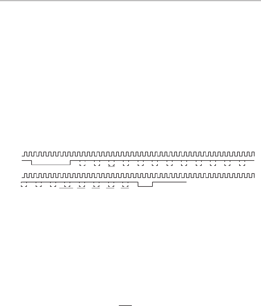
1.1.12.1 Serialized Interrupt Control
Serialized interrupt signaling is described below.
Figure 1–2. Serialized Interrupt Signal
IRQ0 IRQ1 SMI IRQ3 IRQ4 IRQ5 IRQ6 IRQ7 IRQ8 IRQ10 IRQ11 IRQ12
IRQ13 IRQ14 IRQ15 IOCHCK INTA INTB INTC INTD STOP Frame
START Frame
PCLK
IRQSER
PCLK
IRQSER
The start frame width may vary from four to eight PCI clock cycles. The STOP
frame width is two clock cycles for quiet mode and three clock cycles for
continuous mode. Default mode is continuous mode for all slave devices and
a host device. PIIX4 does not support IRQ0, IRQ8, and IRQ13.
The PCI445X can generate serial IRQ frames for ISA and PCI interrupts.
Below are related registers and their definitions.
INTMODE bits (device control register, PCI offset 92h, bits 2–1). Select
interrupt mode
SER_STEP bits (system control register, PCI offset 80h, bits 31–30).
Change PCI interrupt data frame (serial interrupts only)
INTRTIE bit (system control register, PCI offset 80h, bit 29). Tie CardBus
PCI interrupts to INTA
TIEALL bit (system control register, PCI offset 80h, bit 28). Tie all PCI
interrupts internally
Refer to the
Serialized IRQ Support for PCI Systems
specification,
revision 6.0.
1.1.12.2 CSC Interrupt Routing for Windows Compatibility
The CSC interrupt routing control bit (diagnostic register, PCI offset 93h, bit 5)
should be set to 1 (default) to keep Windows compatibility.

System Features Selection
1-6
1.1.12.3 Asynchronous CSC Interrupt Generation
The ASYNC_CSC bit (diagnostic register, PCI offset 93h, bit 0) controls the
CSC interrupt signaling method. If this bit is set to 0, then CSC is generated
synchronously to PCLK (recommended). By default this bit is set to 1, which
is the asynchronous mode.
1.1.12.4 CardBus Reserved Terminal Signaling
The CardBus interface has reserved terminals. Usually the CardBus controller
drives these terminals low. If the CBRSVD bit (system control register, PCI
offset 80h, bit 22) is set to 0, then the CardBus reserved terminal signals are
in a high-impedance state when a CardBus card is inserted in the socket.
1.1.12.5 Memory Burst R/W Operation Control
Memory read bursting is controlled via the MRBURSTDN bit (system control
register, PCI offset 80h, bit 15) for downstream burst transactions (PCI-to-PC
Card) and the MRBURSTUP bit (system control register, PCI offset 80h,
bit 14) for upstream burst transactions (PC Card-to-PCI). Memory write
bursting is controlled via the POSTEN bit (bridge control register, PCI offset
3Eh, bit 10). This bit enables write posting if disabled. No write data can be
accepted (including burst writes) until any previous write data has been
forwarded to its destination. By default, write posting and upstream read bursts
are disabled.
1.1.12.6 Power Savings Mode
The PCI445X device has a proprietary power-saving mode. It can be disabled
by changing the PWRSAVINGS bit (system control register, PCI offset 80h,
bit 6) to 0. When this bit is enabled (default), PCI CLOCK is internally gated
for a nonfunctioning circuit. For example, the CardBus interface does not
function when a 16-bit card is inserted. This power-saving mode will not
degrade performance; therefore, the default setting is recommended.
1.1.12.7 PME/RI_OUT Terminal Control Clarification
PME/RI_OUT terminal can be set up to signal a combination of these events.
The terminal is set up using the PME/RI_OUT bit (system control register, PCI
offset 80h, bit 0), the RIENB bit (card control register, PCI offset 91h, bit 7), and
PME enable bit (power management control/status, PCI offset A4h, bit 8). If
the terminal is set up as RI_OUT and RIENB has ring indicate enabled, then
this signal follows the RI_OUT signal for 16-bit I/O cards. If RIENB has ring
indicate disabled but PME has PME enabled, then this line reflects the state
of the PMESTAT bit (power management control/status, PCI offset A4h,
bit 15). If both PME and ring indicate are disabled, then the line remains high.
If the line is configured as PME and PME is enabled, then this line follows the
state of the PMESTAT bit; otherwise, the line remains high.
1.1.12.8 CLKRUN Control
PCLK can be kept running using CLKRUN protocol by setting the KEEPCLK
bit (system control register, PCI offset 80h, bit 1) to 1.

System Features Selection
1-7
PCI445X Device
CCLK can be slowed down rather than stopped by CCLKRUN. If CCLKRUN
is set, the CLKCTRLEN (CardBus socket 20h, bit 16) and CLKCTR (CardBus
socket 20h, bit 0) bits are both set to 1. The clock is slowed down to 1/16. In
this mode the PCI clock is not allowed to stop.
1.1.12.9 SMI
A PC card power change event can be reported to the system as SMI (IRQ2
or CSC). It can be controlled with the SMIROUTE, SMISTATUS, and SMIENB
bits (system control register, PCI offset 80h, bits 26, 25, and 24, respectively).
1.1.12.10 Socket Power Lock
Socket power can be protected from software control in the D3hot state. It can
be done with the socket power lock bit (device control register, PCI offset 92h,
bit 7).
1.1.12.11V
CC
Protection
The VCCPROT bit (system control register, PCI offset 80h, bit 21) controls VCC
protection for 16-bit cards. This feature protects applying the wrong (higher)
VCC to the 16-bit card. If a 3.3-V-only card is inserted, then it protects against
applying 5 V to the card. Default is 0 (enabled).
1.1.12.12 ZV Port Control and Auto Detect Function
Internal zoomed video buffers can be controlled with the ZV autodetect
function. It can be turned on by setting the zoomed video autodetect bit
(multimedia control register, PCI offset 84h, bit 5) to 1. Autodetect priority
encoding bits (multimedia control register, PCI offset 84h, bits 4–2) can control
the priority scheme.

System Implementation
1-8
1.2 System Implementation
This section describes signal connection for each interface, PCI bus, PC card
interface, I2C interface, P2C interface, ZV interface, interrupt interface (parallel
and serial), miscellaneous signals, and the PHY-Link interface. It also explains
pullup/pulldown resistor requirements.
1.2.1 Clamping Rails
The PCI445X device has three clamping rails: VCCA, VCCB, and VCCP. VCCA
and VCCB are not power supplies for PC cards. After a card is powered up, the
supply voltage to the card is fed back into the VCCA (or VCCB) input to the
controller. This provides the controller a clamping level for signals to the card.
Technically the power switch controlling VCCA is also supplying power to the
card via this signal, but actually VCCA is not a signal via which the controller
supplies power to the card.
The PCI445X device only drives out a maximum signal of 3.3 V due to the
3.3-V core. This is not a problem, as 3.3 V is still seen as a logic 1 to a 5-V
system.
VCCA and VCCB
PC Card interface clamping rails. CD1, CD2, VS1, VS2, and STSCHG/RI
are not clamped, because these terminals should be able to signal without
VCCA/VCCB.
VCCP
PCI bus interface clamping rail. It includes the MFUNC7/LOCK,
MFUNC7–MFUNC0, IRQSER, GRST, and P2C terminals. It excludes
INTA, INTB, INTC, and PME.
Note:
The PME/RI_OUT terminal uses an open drain (OD) buffer.
1.2.2 PCI Bus Interface
PCLK, AD31–AD0, C/BE3–C/BE0, PAR, DEVSEL, FRAME, STOP,
TRDY, IRDY, GNT, REQ
These terminals can be connected to the system PCI bus directly. GNT
and REQ are dedicated signals from the PCI bus arbitrator.
PERR, SERR, and LOCK
PERR and SERR are required signals. LOCK is an optional signal and
available in MFUNC1, MFUNC3, and MFUNC7.
IDSEL
If there is a pulldown on LATCH, then the IDSEL will be routed to AD23, but
the consequence of this is that the system designer must use AD23 as

System Implementation
1-9
PCI445X Device
IDSEL, there is no alternative. If another AD line is to be used for IDSEL,
then the system designer must leave the pullup off LATCH and use
MFUNC7 to route IDSEL. Also, if AD23 is used, then the resistive coupling
should not be used.
Refer to the
Implementation Note: System Generation of IDSEL
in the
PCI
Local Bus Specification, Revision 2.2 (section 3.2.2.3.5)
.
PCI Local Bus
Specification, Revision 2.2 (section 4.2.6, footnote 31)
recommends
resistive coupling. A 100-Ω resistor is recommended.
PRST (PCI reset) and G_RST (Global reset)
G_RST initializes all of the registers and state-machines of the PCI445X
device, and PRST does not. G_RST should be asserted during power-on
and rebooting. It puts the PCI445X device into the initialized state. PRST
does not initialize global-reset-only bits and, if PME is enabled, PME
context bits. Refer to Table A–1, Global Reset Only Cleared Bits, and
Table A–2, PME Context Bits. PRST is connected to PCI RESET; G_RST
requires a special signal in the motherboard. It will come from the chipset.
If the system does not support wake-up from D3cold, then PRST and
G_RST can be tied together. Note that G_RST and PRST are clamped to
VCCP.
INTA, INTB, and INTC
When using one of the parallel PCI interrupt modes, INTA, INTB, and INTC
should be connected to the PCI interrupt lines. If the INTRTIE bit (system
control register, PCI offset 80h, bit 29) is set, then both CardBus functions
(functions 0 and 1) will signal and report INTA, and only INTA and INTC will
need to be routed. If the TIEALL bit (system control register, PCI offset
80h, bit 28) is set, then all functions (0, 1, and 2) will report INTA and INTA
will be the only interrupt required.
CLKRUN
This signal is optional. However, if saving power is a concern, this signal
should be implemented. Refer to the
PCI Mobile Design Guide
Revision 1.1 (Section 2)
.
PME
This signal is required for the ACPI systems. In a notebook PC, this signal
is usually connected to the south bridge (ex., PIIX4) or embedded
controller (EC). The PME terminal uses an open-drain type buffer.
Note: Pullup Resistor Requirements
A pullup resistor is required for each of the following terminals: IRDY, TRDY,
FRAME, STOP, DEVSEL, PERR, SERR, LOCK, PRST, G_RST, INTA, INTB,
INTC, CLKRUN, and PME.
System Implementation
1-10
1.2.3 PC Card Interface
The PC Card interface has two modes: the 16-bit interface mode and the
CardBus 32-bit interface mode.
Damping resistor on CCLK terminal
A series-damping resistor is recommended on the CCLK signal. The
damping resistor is system dependent. If line impedance is in the 60–90-Ω
range, a 47-Ω resistor is recommended (see
PC Card Standard,
Revision 7
).
CD line filtering
PCI445X device has the advanced CDx line filtering circuit. It provides
90 µs of noise immunity. A 270-pF filtering capacitor is still recommended
for each of the power supply terminals: VCC, VCCS, and VCCP.
Socket power supply
Socket power is supplied through TPS22X6 power switches. The
PCI445X device requires VCCA and VCCB for the protection of the other
device(s) on the bus.
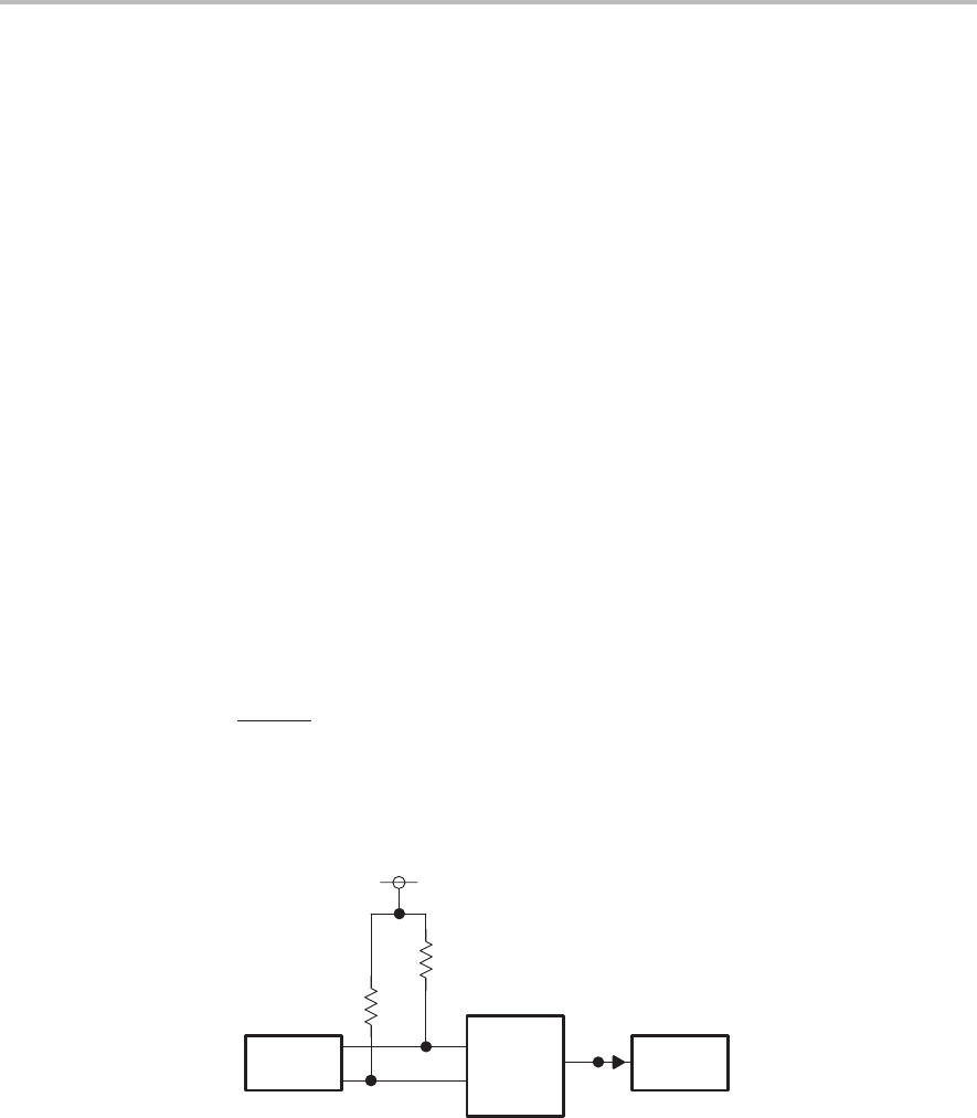
1.2.4 2-Wire (I2C) Interface for EEPROM
The PCI445X device can load configuration registers from EEPROM after
G_RST assertion. The SDA and SCL lines require pullup resistors to enable
this function. Depending on the EEPROM requirements, the SDA and SCL
lines must be pulled up to 3.3 V or 5 V.
Figure 1–3. EEPROM 2-Wire Interface
EEPROM SDA
SCL
PCI445X TPS22X6
EEPROM slave address should be 101 0000b.

System Implementation
1-11
PCI445X Device
Table 1–1.Registers and Bits Loadable Through Serial EEPROM
Register Offset Register Bits Loaded From
EEPROM
The following are configuration registers for the OHCI function (function 2)
PCI register (2Ch) PCI subsystem ID 15–0
PCI register (2Dh) PCI vendor ID 15–0
PCI register (3Eh) PCI maximum latency, minimum grant 11–8, 3–0
PCI register (F0h) PCI miscellaneous configuration 15, 13, 10, 3–0
PCI register (F4h) Link enhancements control 7, 2, 1
OHCI register (24h) 1394 global unique ID Hi 31–0
OHCI register (28h) 1394 global unique ID Lo 31–0
The following are configuration registers for PC Card functions (functions 0 and 1)
PCI register (40h) Subsystem vendor ID 15–0
PCI register (42h) Subsystem ID 15–0
PCI register (80h) System control 31–24, 22–14, 6–3, 1, 0
PCI register (86h) General control 3–0
PCI register (89h) General-purpose event enable 7, 6, 3–0
PCI register (8Bh) General-purpose output 3–0
PCI register (8Ch) Multifunction routing 30–28, 26–24, 22–20,
18–16, 14–12, 10–8,
6–4, 2–0
PCI register (91h) Card control 7, 6, 2–0
PCI register (92h) Device control 7, 6, 2–0
PCI register (93h) Diagnostic 7, 5, 0
PCI register (A2h) Power management capabilities 15
PCI register ExCA ID and revision 7–0

System Implementation
1-12
1.3 Sample PCI445X EEPROM Data File
Following is an example EEPROM data file used with the PCI445X device:
;PCI4450 default EEPROM Data File
;Register 0xXX Binary Description
;–––––––– –––– –––––– –––––––––––
00 0x43 ;01000011 PCI max_lat (lower
4 bits)/PCI min gnt (lower 4 bits)
01 0x4C ;01001100 PCI Subsystem Vendor ID (lsbyte) ** Insert
your SSVID LSB
02 0x10 ;00010000 PCI Subsystem Vendor ID (msbyte) ** Insert
your SSVID MSB
03 0x11 ;00010001 PCI Subsystem ID (lsbyte) ** Insert
your SSID LSB
04 0x80 ;10000000 PCI Subsystem ID (Msbyte) ** Insert
your SSID MSB
05 0xC2 ;11000010 Link Enhancement Register/HC Control
defaults
06 0x40 ;01000000 MiniROM_Addr
07 0x56 ;01010110 1394 GUIDHi (lsbyte)** Insert GUIDHi byte
008 0x28 ;00101000 1394 GUIDHi (lsbyte)** Insert GUIDHi byte
109 0x00 ;00000000 1394 GUIDHi (msbyte)** Insert GUIDHi byte
20A 0x08 ;00001000 1394 GUIDHi (msbyte)** Insert GUIDHi byte
30B 0xXX ;XXXXXXXX 1394 GUIDLo (lsbyte)** GUIDLo byte 0 auto
incremented from ;serial.dat
0C 0xXX ;XXXXXXXX 1394 GUIDLo (lsbyte)** GUIDLo byte 1 auto
incremented from ;serial.dat
0D 0xXX ;XXXXXXXX 1394 GUIDLo (msbyte)** GUIDLo byte 2 auto
incremented from ;serial.dat
0E 0xXX ;XXXXXXXX 1394 GUIDLo (msbyte)** GUIDLo byte 3 auto
incremented from ;serial.dat
0F 0xXX ;XXXXXXXX ROM CRC (Calculated by EELynx)
10 0x10 ;00010000 Link_Enh Byte 1
11 0x00 ;00000000 PCI Misc Byte 0
12 0x24 ;00100100 PCI Misc Byte 1
13 0xFF ;11111111 this area reserved
19 0xFF ;11111111
1A 0xFF ;11111111
1B 0xFF ;11111111
1C 0xFF ;11111111

System Implementation
1-13
PCI445X Device
1D 0xFF ;11111111
1E 0xFF ;11111111
1F 0xFF ;11111111
20 0x00 ;00000000 Flag Byte (if 0xFF do not load Function 0
and 1)
21 0x12 ;00010010 SubSys Byte 3 ** Insert your SSVID MSB
22 0x34 ;00110100 SubSys Byte 2 ** Insert your SSVID LSB
23 0x56 ;01010110 SubSys Byte 1 ** Insert your SSID MSB
24 0x78 ;01111000 SubSys Byte 0 ** Insert your SSID LSB
25 0x60 ;01100000 SysCtrl Byte 0
26 0xB0 ;10110000 SysCtrl Byte 1
27 0x44 ;01000100 SysCtrl Byte 2
28 0x08 ;00001000 SysCtrl Byte 3
29 0x00 ;00000000 General Control
2A 0x00 ;00000000 GP Event Enable
2B 0x00 ;00000000 GP Output
2C 0x22 ;00100010 MF Route Byte 0
2D 0x22 ;00100010 MF Route Byte 1
2E 0x22 ;00100010 MF Route Byte 2
2F 0x04 ;00000100 MF Route Byte 3
30 0x02 ;00000010 Card Control
31 0x66 ;01100110 Device Control
32 0x61 ;01100001 Diagnostic
33 0x00 ;00000000 PMC Byte 1
34 0x82 ;10000010 ExCA ID and Rev
System Implementation
1-14
1.3.1 P2C Interface for TPS22X6 Power Switch
The interface between the PCI445X device and TPS22X6 power switch is
serialized to reduce the number of signal lines. The P2C interface requires only
three lines to control the switch. As a PCI445X default, the CLOCK signal is
selected from an external source. It is usually provided from RTC, 32.768 kHz.
The PCI445X device can also generate this clock from an internal ring
oscillator. The typical frequency of the internal ring oscillator is 16 kHz. If using
the internal clock source, then a pulldown resistor is required on the CLOCK
terminal. If arranging for D3 wake implementation, then connect the power
switch RESET terminal to GRST.
Figure 1–4. TPS22X6 Power Switch Interface
Pulldown on
CLOCK
VCCA
VCCB
VPPB
VCCA
VPPA
DATA
CLOCK
PCI445X
VCCB
SLOT
A
SLOT
B
LATCH
TPS22X6
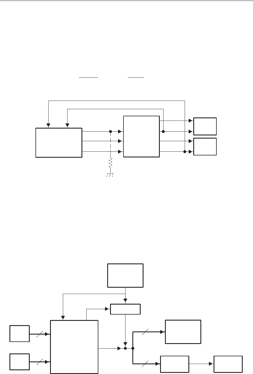
1.3.2 Zoomed Video (ZV) Interface
The PCI445X device has an internally buffered and selectable ZV interface.
It supports three ZV sources, two from PC Cards and one from an external
source. An auto ZV detect function provides software independent ZV
switching. The auto ZV detect function senses the pixel clocks, arbitrates three
inputs, and selects one of them according to priority bits.
Figure 1–5. Example of a ZV Interface
23
SLOT
B
SLOT
A
PCI445X
Buffer
3rd ZV
Source
ZVSTATZVPCLK
Sound
Controller
Stereo
Audio
Codec
Graphic
Controller
23
19
4

System Implementation
1-15
PCI445X Device
If the third ZV source is not implemented, ZVPCLK and ZVSTAT are not
required. To support ZV audio, an audio codec device is required for L and R
sound decoding.
1.3.3 Interrupt Signaling Interface
Serialized Interrupt Interface
The serialized interrupt (ISA and PCI) interface is a single-line interface,
IRQSER. A pullup resistor is required on this terminal. The signal is
synchronous to PCLK, so PCLK is a required signal. Please remember
that SUSPEND gates PCLK internally. Usually this signal is connected to
the south bridge (ex., PIIX4). The IRQSER signal is sharable with other
devices.
Parallel PCI Interrupt
See Section 1.2.2, PCI Bus Interface.
1.3.4 Miscellaneous Signals
1.3.4.1 SUSPEND
The SUSPEND signal gates the PRST and G_RST signals from the PCI445X
device. SUSPEND also gates PCLK inside the PCI445X device in order to
minimize power consumption. Gating PCLK makes the IRQSER state
machine stop until SUSPEND is deasserted. Two requirements for
implementing suspend mode are that the PCI bus must not be parked on the
PCI445X device and IRQSER signaling is not proceeding when SUSPEND is
asserted.
1.3.4.2 RI_OUT and PME
RI_OUT can be programmed on the RI_OUT/PME or MFUNC7 terminal. PME
can be programmed only on the RI_OUT/PME terminal. To support both
RI_OUT and PME in a system, the RI_OUT/PME terminal must be
programmed as PME. These signals are usually connected to the south bridge
(ex., PIIX4) or an embedded controller (EC). Buffers of the RI_OUT/PME type
are open-drain; therefore, a pullup resistor is required on this terminal.
1.3.4.3 SPKROUT
SPKROUT is a dedicated terminal and it is usually mixed to PC sound, and
connected to a sound device.
1.3.4.4 Activity LEDs
Activity LEDs can be programmed on MFUNC terminals. These signals are
active-high and driven for 64 ms duration.
1.3.4.5 Distributed DMA (DDMA)
The PCI445X device supports both PC/PCI (centralized) DMA and a
distributed DMA slave engine for 16-bit PC Card DMA support.
System Implementation
1-16
Figure 1–6. Distributed DMA Signal Connection
PCGNT
PCREQ
PCI445X
South
Bridge
(ex., PIIX4)
1.3.5 Requirement of Pullup/Pulldown Resistors
Note:
The PCI445X device has integrated pullup resistors and does not require
external pullups.
Table 1–2.PC Card Interface Pullup Resistor List
†‡
Terminal Name
(16-bit Memory PC Card)
Terminal Name
(16-bit I/O PC Card)
Terminal Name
(CardBus PC Card) Pull Up to Voltage
CD1 CD1 CCD1 VCC
CD2 CD2 CCD2 VCC
VS1 VS1 CVS1 VCC
VS2 VS2 CVS2 VCC
A19 A19 CBLOCK VCCA or VCCB
A20 A20 CSTOP VCCA or VCCB
A21 A21 CDEVSEL VCCA or VCCB
A22 A22 CTRDY VCCA or VCCB
RESET RESET CRST VCCA or VCCB
WAIT WAIT CSERR VCCA or VCCB
RFU INPACK CREQ VCCA or VCCB
BVD2 SPKR CAUDIO VCCA or VCCB
BVD1 STSCHG CSTSCHG VCCA or VCCB
A14 A14 CPERR VCCA or VCCB
READY IREQ CINT VCCA or VCCB
A15 A15 CIRDY VCCA or VCCB
WP IOIS16 CCLKRUN VCCA or VCCB
†The PCI445X device has integrated pullup resistors and does not require external pullups.
‡CFRAME needs a pullup resistor, but it should be implemented on each PC Card.
System Implementation
1-17
PCI445X Device
Table 1–3.PCI Bus Interface Pullup Resistor List
PCI Signal Pull-Up Voltage
FRAME VCCP
TRDY VCCP
IRDY VCCP
DEVSEL VCCP
STOP VCCP
SERR VCCP
PERR VCCP
LOCK VCCP
INTA
INTB
INTC VCCP
CLKRUN VCCP
PRST VCCP
G_RST VCCP
PME System dependent
The pullup/pulldown on MFUNC depends on how it is implemented. Some
signals may require pullups, others pulldowns, and for a GPI or GPO only the
system designer would know how that line should be pulled.
Table 1–4.Miscellaneous Terminals Pullup Resistor List
PCI Signal Required Situation Pullup/Pulldown
Voltage
MFUNC7–MFUNC4 N/C or used as output VCCP or GND
MFUNC3–MFUNC0
(GPIO3–GPIO0) N/C or used as output VCCP or GND
MFUNC7(LOCK)N/C or used as output VCCP
CLOCK Internal OSC is selected GND
LATCH If MFUNC7 is used for IDSEL GND
IRQSER VCCP
RI_OUT/PME System dependent
SUSPEND System dependent
Note: Removing clamping voltage makes all the clamped signals low.

System Implementation
1-18
Table 1–5.Required Pullup/Pulldown Resistors
Signal Resistor Recommended
Value (Ω)Condition
LPS Pulldown (Default) 1.0 k Required
Note: All pullup/pulldown resistor value recommendations are provided as guidelines only. The best value for an individual
design varies depending upon board characteristics, standard design rules and practices, etc.

System Implementation
1-19
PCI445X Device
1.4 BIOS Considerations
1.4.1 Initialization
This section explains which registers require initialization, but does not
discuss detailed information about the registers themselves. Refer to the
corresponding specifications.
Reference white paper:
http://www.microsoft.com/hwdev/busbios/cardbus1.htm
1.4.1.1 PCI Standard Registers Initialization
Command register (PCI offset 04h: 16-bit)
Set to 0007h (enables bus master control, memory space control, and I/O
space control)
Cache line size register (PCI offset 0Ch: 8-bit)
Set to 08h (It is dependent on host-to-PCI bridge specification). It enables
memory read line and memory read multiple command.
Latency timer (PCI offset 0Dh: 8-bit)
This register should reflect each PC Card requirement, but Windows does
not do so. Therefore, system imlementers should determine the value. A
detailed description of this register is in the
PCI Local Bus Interface
Specification
. Typical setting for this register is 40h.
CardBus socket registers/ExCA base address (PCI offset 10h: 32-bit)
It should be set to 0000 0000h (default).
CardBus latency timer register (PCI offset 1Bh: 8-bit)
Setup of this register is not required because the CardBus bus is a
single-device bus, and the PCI445X device does not deassert CGNT until
a transaction is finished. (It does not mean that the PCI445X device
continues the transaction. The PCI445X device would terminate and
disconnect or abort the transaction as required).
Memory and I/O windows (PCI offset 1Ch – 3Fh)
All memory and I/O windows should be closed (set to base > limit).
Interrupt line register (PCI offset 3Ch: 8-bit)
This register is set to FFh (default).
Subsystem vendor ID and subsystem ID registers (PCI offsets 40h
and 42h: 16-bit/16-bit)
These registers can be set through EEPROM or BIOS. These registers
are read-only as default. Before writing to the registers, the SUBSYSRW
bit (system control register, PCI offset 80h, bit 5) should be set to 1. After
setting up the registers, the SUBSYSRW bit should be set 0 to protect

System Implementation
1-20
against unexpected overwriting. The values are system and vendor
dependent.
PC Card 16-bit I/F legacy mode base address register (PCI offset 44h:
32-bit)
Set to 0000 03E1h (16-bit mode) and set to 0000 0001 (CardBus mode) in
response to a disable call.
Power management capabilities register (PCI offset A2h: 16-bit)
If the system does not support VAUX in D3cold state, then clear bit 15.
Power management control/status register (PCI offset A4h: 16-bit)
Clear bit 15 by writing a 1. This should be done after all the other
initialization for the PCI445X device is finished. Make sure that the
PCI445X device is in the D0 state, especially after reboot.
1.4.1.2 PCI TI Proprietary Registers Initialization
The registers listed below should be set up according to system requirements.
Refer to Section 1.1.12.
System control register (PCI offset 80h: 32-bit)
Multimedia control register (PCI offset 84h: 8-bit)
GPIO3–GPIO0 control registers (PCI offset 88h – 8Bh: 8-bit)
Multifunction routing register (PCI offset 8Ch: 32-bit)
Card control register (PCI offset 91h: 8-bit)
Device control register (PCI offset 92h: 8-bit)
Diagnostic register (PCI offset 93h: 8-bit)
DMA socket register 0 and 1 (PCI offset 94h, 98h: 32-bit)
GPE control/status register (PCI offset A8h: 16-bit)
ExCA identification and revision (ExCA offset 800h: 8-bit)
Socket power management register (CardBus socket registers offset 20h:
32-bit)
1.4.2 System Sleeping State Consideration
Supporting sleeping states, such as SUSPEND, STANDBY, and
HIBERNATION are important for a notebook PC environment. The following
describes the sleeping state in APM systems:
1) SUSPEND
Reset signals G_RST and PRST are gated while SUSPEND is asserted.
Power consumption of the PCI445X device is low if SUSPEND is asserted.

System Implementation
1-21
PCI445X Device
2) Register save/restore
Register content is not preserved in the sleeping state (it depends on the
system implementation). Therefore, BIOS should restore the register
content. Under Windows98, most of the register content is saved and
restored by the pci.vxd and cbss.vxd.
3) Troubleshooting tips for sleep/resume issues
Symptoms of sleep/resume issues are:
System hung up during resume
PC Card does not work after resume
PC Card is not recognized after resume
The probable reason for these problems is that the register content is not
preserved correctly. Checking the register content before taking the system to
the sleep mode and after resuming from the sleep mode may shed some light.
If some of the register settings are not the same after resuming from the sleep
mode, then the BIOS most likely did not restore those values.
1.4.3 Docking System Consideration
Subsystem IDs can be assigned as long as the SUBSYSRW bit (system
control register, PCI offset 80h, bit 5) is set. It is better to do this from EEPROM
as no driver will be running to set the SSID up after a hot-dock/warm-dock.
Therefore, the IDs should be loaded through the I2C interface using an
EEPROM.
Important Information
1-22
1.5 Important Information
This section clarifies important system implementation.
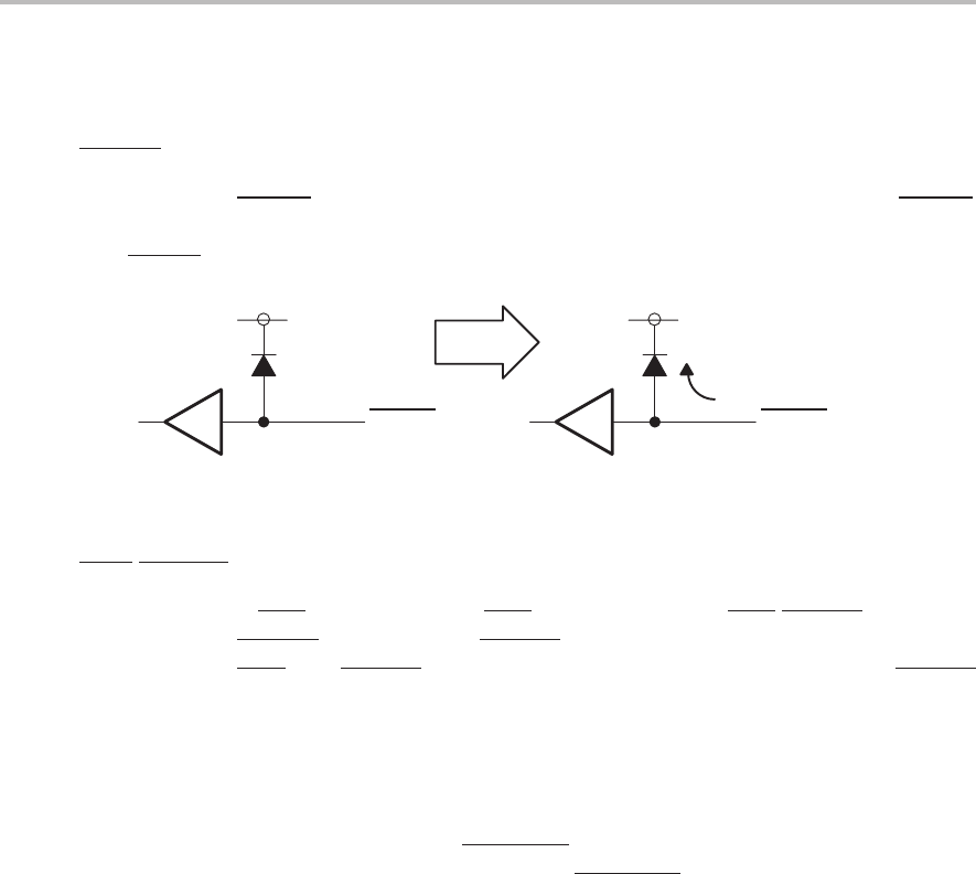
1.5.1 G_RST Clamping Rail
G_RST is clamped to VCCP, so removing VCCP causes assertion of G_RST.
Figure 1–7.
G_RST and V
CCP
Relationship
VCCP
G_RST
VCCP = 0
VCCP
removed
G_RST
All other signals with clamping rails behave the same way.
1.5.2 PME/RI_OUT Bit Definition
If PME is selected, only PME is signaled on the PME/RI_OUT terminal. If
RI_OUT is selected, only RI_OUT is signaled. The PCI445X device can signal
PME and RI_OUT as completely separated signals. In this case RI_OUT
should be assigned on the MFUNC terminal.
1.5.3 Serialized IRQ Data Stream
PCI clock is needed for operation of the PCI445X serialized IRQ
state-machine. During SUSPEND assertion, the PCI445X device stops the
IRQSER stream. Before asserting SUSPEND, IRQSER must be stopped.
1.5.4 Socket Power Control
An internal or external CLOCK source is needed for the socket power control
through the P2C interface. The internal ring oscillator is on while the core VCC
is applied to the PCI445X device. External CLOCK source is dependent on the
system.
1.5.5 External CLOCK Frequency for P2C Interface
If an external P2C CLOCK is used, then it will affect:
Advanced CD line noise filtering
VS test speed
TPS22X6 power control interface speed
Use of the internal ring oscillator is recommended. Recommended external
CLOCK source is the 32.768-kHz real-time clock (RTC).

Global Reset Only Bits/PME Context Bits
A-1
Global Reset Only Bits, PME Context Bits
Global Reset Only Bits, PME Context Bits
Topic Page
A.1 Global Reset Only Bits/PME Context Bits A-2
Appendix A

Global Reset Only Bits/PME Context Bits
A-2
A.1 Global Reset Only Bits/PME Context Bits
Table A–1.Global Reset Only Cleared Bits
Register Name Space Offset Bit
Subsystem IDs PCI 40h 31–0
PC card 16-bit legacy mode base address PCI 44h 31–1
System control PCI 80h 31–29, 27–24, 22–14, 6–3,
1–0
Multimedia control PCI 84h 7–0
General status PCI 85h 2–0
GPIO0 control PCI 88h 7, 6, 4, 3, 1, 0
GPIO1 control PCI 89h 7, 6, 3, 1, 0
GPIO2 control PCI 8Ah 7, 6, 4, 3, 1, 0
GPIO3 control PCI 8Bh 7, 6, 3, 1, 0
MFUNC routing PCI 8Ch 31–0
Retry status PCI 90h 7–1
Card control PCI 91h 7, 6, 2, 1, 0
Device control PCI 92h 7–0
Diagnostic PCI 93h 7–0
Socket DMA register 0 PCI 94h 1–0
Socket DMA register 1 PCI 98h 15–0
GPE control/status PCI A8h 10, 9, 8, 2, 1, 0
Note: The following link registers are reset by global reset only.
PCI subsystem identification register—PCI offset 2Ch
MIN_GNT and MAX_LAT register—PCI offset 3Eh
PCI OHCI control register—PCI offset 40h
Power management control and status register—PCI offset 48h
PCI miscellaneous and configuration register—PCI offset F0h
Link enhancement control register—PCI offset F4h
However, there is no support in the OS for the PME-type wake events of the
1394 peripherals at this time.
Global Reset Only Bits/PME Context Bits
A-3
Global Reset Only Bits, PME Context Bits
Table A–2.PME Context Bits
Register Name Space Offset Bit
Bridge control PCI 3Eh 6
Power management capabilities PCI A2h 15
Power management control/status PCI A4h 15, 8
ExCA power control ExCA 802h, 842h 4, 3, 1, 0
ExCA interrupt and general control ExCA 803h/843h 6
ExCA card status change ExCA 804h/844h 3, 2, 1, 0
ExCA card status change interrupt ExCA 805h/845h 3, 2, 1, 0
CardBus socket event CardBus 00h 3, 2, 1, 0
CardBus socket mask CardBus 04h 3, 2, 1, 0
CardBus socket status CardBus 10h 6, 5, 4, 2, 1, 0
Global reset only bits are cleared (to default value) only when G_RST is
asserted.
PME context bits are not cleared (to default value) by PRST if the PME_EN
bit is set to 1.
Both G_RST and PRST can be gated by asserting the SUSPEND signal.

A-4
B-1
PME and RI Behavior
PME and RI Behavior
This appendix clarifies PME and RI signal behavior. These signals are
important to support the wake-up event from a PC Card (CardBus and 16-bit
cards.)
Topic Page
B.1 PME and RI Behavior B-2
Appendix B

B-2
B.1 PME and RI Behavior
Table B–1.CardBus CTSCHG and Wake-Up Signals Truth Table
RINGEN RIMUX RIENB PME_EN PME_STAT RI_OUT/PME MFUNC7
0 0 0 0 Latched ––– –––
0 0 0 1 Latched Latched CSTSCHG –––
0 0 1 0 Latched ––– –––
0 0 1 1 Latched ––– –––
0 1 0 0 Latched ––– –––
0 1 0 1 Latched Latched CSTSCHG –––
0 1 1 0 Latched ––– –––
0 1 1 1 Latched Latched CSTSCHG –––
1 0 0 0 Latched ––– –––
1 0 0 1 Latched Latched CSTSCHG –––
1 0 1 0 Latched CSTSCHG CSTSCHG
1 0 1 1 Latched CSTSCHG CSTSCHG
1 1 0 0 Latched ––– –––
1 1 0 1 Latched Latched CSTSCHG –––
1 1 1 0 Latched ––– CSTSCHG
1 1 1 1 Latched Latched CSTSCHG CSTSCHG
Table B–2.16-Bit Card RI/STSCHG and Wake-Up Signals Truth Table
RINGEN RIMUX RIENB PME_EN PME_STAT RI_OUT/PME MFUNC7
0 ––– ––– ––– ––– ––– –––
1 0 0 0 Latched ––– –––
1 0 0 1 Latched Latched RI –––
1 0 1 0 Latched RI RI
1 0 1 1 Latched RI RI
1 1 0 0 Latched ––– –––
1 1 0 1 Latched Latched RI –––
1 1 1 0 Latched ––– RI
1 1 1 1 Latched Latched RI RI
PCI445X Buffer Types
C-1
PCI445X Buffer Types
PCI445X Buffer Types
Topic Page
C.1 PCI445X Buffer Types C-2
Appendix C
PCI445X Buffer Types
C-2
C.1 PCI445X Buffer Types
Table C–1. PCI445X Terminal Function Assignment and Buffer Types
Signal Name Terminal Type Signal Name Terminal Type
A_CAD0 B8 TS A_CAD28 N2 TS
A_CAD1 A7 TS A_CAD29 N3 TS
A_CAD2 C8 TS A_CAD30 P1 TS
A_CAD3 A6 TS A_CAD31 D9 TS
A_CAD4 B7 TS A_CAUDIO M1 I
A_CAD5 B6 TS A_CBLOCK D2 P
A_CAD6 C7 TS A_CC/BE0 A4 TS
A_CAD7 D7 TS A_CC/BE1 C3 TS
A_CAD8 C6 TSO A_CC/BE2 F2 TS
A_CAD9 C5 TS A_CC/BE3 J1 TS
A_CAD10 B4 TS A_CCD1 A8 I
A_CAD11 A3 TS A_CCD2 M4 TS
A_CAD12 C4 TS A_CCLK E3 TS
A_CAD13 D5 TS A_CLKRUN M3 STS
A_CAD14 B2 TS A_CDEVSEL D1 STS
A_CAD15 B3 TS A_CFRAME G4 STS
A_CAD16 A2 TS A_CGNT C1 STS
A_CAD17 F1 TS A_CINT L2 I
A_CAD18 G3 TS A_CIRDY E1 STS
A_CAD19 G2 P A_CPAR C2 TS
A_CAD20 H3 TS A_CPERR D3 STS
A_CAD21 H1 TS A_CREQ J3 I
A_CAD22 J4 TS A_CRST H2 O
A_CAD23 J2 TS A_CSERR L3 I
A_CAD24 K2 TS A_CSTOP E4 STS
A_CAD25 K3 TS A_CSTSCHG M2 I
A_CAD26 K1 TS A_CTRDY E2 STS
A_CAD27 N1 TS A_CVS1 L1 I/O
Note: The voltage sense terminals (VS1/CVS1, VS2/CVS2) are always driven low except under the following conditions:
1) High-impedance state during RESET
2) Toggle during socket interrogation

PCI445X Buffer Types
C-3
PCI445X Buffer Types
Table C–1. PCI445X Terminal Function Assignment and Buffer Types (Continued)
Signal Name Terminal Type Signal Name Terminal Type
A_CVS2 G1 I/O AD25 N20 TS
A_RSVD A5 TS AD26 M17 TS
A_RSVD B1 TS AD27 M18 TS
A_RSVD P2 TS AD28 M19 TS
AD0 V13 TS AD29 M20 TS
AD1 Y14 TS AD30 L19 TS
AD2 W14 TS AD31 L18 TS
AD3 Y15 TS B_CAD0 J19 TS
AD4 W15 TS B_CAD1 J17 TS
AD5 Y16 TS B_CAD2 J18 TS
AD6 U14 TS B_CAD3 H19 TS
AD7 V15 TS B_CAD4 H20 TS
AD8 Y17 TS B_CAD5 G20 TS
AD9 V16 TS B_CAD6 H18 TS
AD10 W17 TS B_CAD7 F20 TS
AD11 Y18 TS B_CAD8 G18 TS
AD12 U16 TS B_CAD9 E20 TS
AD13 V17 TS B_CAD10 G17 TS
AD14 W18 TS B_CAD11 F18 TS
AD15 Y19 TS B_CAD12 E18 TS
AD16 T18 TS B_CAD13 D20 TS
AD17 T19 TS B_CAD14 C20 TS
AD18 T20 TS B_CAD15 D19 TS
AD19 R18 TS B_CAD16 E17 TS
AD20 P17 TS B_CAD17 C16 TS
AD21 R19 TS B_CAD18 B16 TS
AD22 R20 TS B_CAD19 A16 TS
AD23 P18 TS B_CAD20 D14 TS
AD24 N19 TS B_CAD21 A15 TS
Note: The voltage sense terminals (VS1/CVS1, VS2/CVS2) are always driven low except under the following conditions:
1) High-impedance state during RESET
2) Toggle during socket interrogation
PCI445X Buffer Types
C-4
Table C–1. PCI445X Terminal Function Assignment and Buffer Types (Continued)
Signal Name Terminal Type Signal Name Terminal Type
B_CAD22 C14 TS B_CSERR B11 STS
B_CAD23 A14 TS B_CSTOP A20 STS
B_CAD24 A13 TS B_CSTSCHG A11 I
B_CAD25 D12 TS B_CTRDY C17 STS
B_CAD26 C12 TS B_CVS1 B12 I/O
B_CAD27 C10 TS B_CVS2 C15 I/O
B_CAD28 D10 TS B_RSVD C9 TS
B_CAD29 A9 TS B_RSVD C19 TS
B_CAD30 B9 TS B_RSVD G19 TS
B_CAD31 D9 TS C/BE0 W16 TS
B_CAUDIO C11 I C/BE1 V18 TS
B_CBLOCK C18 STS C/BE2 U20 TS
B_CC/BE0 F19 TS C/BE3 N18 TS
B_CC/BE1 D18 TS CLKRUN K18 O
B_CC/BE2 A17 TS CLOCK U12 O
B_CC/BE3 C13 I DATA V12 O
B_CCD1 J20 I DEVSEL U19 STS
B_CCD2 B10 I FRAME V20 STS
B_CCLK B17 TS G_RST Y12 I
B_CDEVSEL B18 STS GND A1 P
B_CFRAME A18 STS GND D4 P
B_CGNT A19 O GND D8 P
B_CINT A12 I GND D13 P
B_CIRDY D16 STS GND D17 P
B_CLKRUN A10 STS GND H4 P
B_CPAR B20 TS GND H17 P
B_CPERR B19 STS GND N4 P
B_CREQ B14 I GND N17 P
B_CRST B15 O GND U4 P
Note: The voltage sense terminals (VS1/CVS1, VS2/CVS2) are always driven low except under the following conditions:
1) High-impedance state during RESET
2) Toggle during socket interrogation

PCI445X Buffer Types
C-5
PCI445X Buffer Types
Table C–1. PCI445X Terminal Function Assignment and Buffer Types (Continued)
Signal Name Terminal Type Signal Name Terminal Type
GND U8 P PHY_DATA6 U9 TS
GND U13 P PHY_DATA7 V9 TS
GND U17 P PHY_LREQ Y5 O
GNT K20 I PME/RI_OUT Y13 OD
IDSEL/MFUNC7 P20 I/O PRST K19 I
IRDY T17 STS REQ L20 O
IRQSER W13 TS SCL W10 TS
LATCH W12 TS SDA Y9 TS
LINKON Y6 I SERR Y20 OD
LPS W5 O SPKROUT V11 O
MFUNC0 W11 I/O STOP V19 STS
MFUNC1 Y11 I/O SUSPEND U11 I
MFUNC2 Y10 I/O TRDY U18 STS
MFUNC3 V10 I/O VCCA B5 P
MFUNC4 W9 I/O VCCA F3 P
MFUNC5 V5 I/O VCCA L4 P
MFUNC6 Y4 I/O VCCB B13 P
PAR W19 STS VCCB E19 P
PCLK K17 I VCCP P19 P
PERR W20 STS VCCP V14 P
PHY_CLK V6 I VCC3.3 D6 P
PHY_CTL0 U7 TS VCC3.3 D11 P
PHY_CTL1 W6 TS VCC3.3 D15 P
PHY_DATA0 V7 TS VCC3.3 F4 P
PHY_DATA1 W7 TS VCC3.3 F17 P
PHY_DATA2 Y7 TS VCC3.3 K4 P
PHY_DATA3 V8 TS VCC3.3 L17 P
PHY_DATA4 W8 TS VCC3.3 R4 P
PHY_DATA5 Y8 TS VCC3.3 R17 P

PCI445X Buffer Types
C-6
Table C–1. PCI445X Terminal Function Assignment and Buffer Types (Continued)
Signal Name Terminal Type Signal Name Terminal Type
VCC3.3 U6 P ZV_UV4 W1 TSO
VCC3.3 U10 P ZV_UV5 Y1 TSO
VCC3.3 U15 P ZV_UV6 W2 TSO
ZV_HREF P3 TSO ZV_UV7 Y2 TSO
ZV_LRCLK V4 TSO ZV_VSYNC R2 TS
ZV_MCLK W4 TSO ZV_Y0 T1 TSO
ZV_PCLK Y3 TSO ZV_Y1 P4 TSO
ZV_SCLK W3 TSO ZV_Y2 R3 TSO
ZV_SDATA U5 TSO ZV_Y3 T2 TSO
ZV_UV0 T4 TSO ZV_Y4 U1 TSO
ZV_UV1 V2 TSO ZV_Y5 T3 TSO
ZV_UV2 U3 TSO ZV_Y6 U2 TSO
ZV_UV3 V3 TSO ZV_Y7 V1 TSO

PCI445X Buffer Types
C-7
PCI445X Buffer Types
Table C–2. Buffer Type Abbreviations
Buffer Type Description
I/O Standard input/output
IStandard input only
OStandard output only
OD Open drain
PPower, GND, or clamp rail
STS Sustained 3-state bidirectional. An active-low signal must be driven high for one cycle
before deasserting.
TS 3-state bidirectional
TSO 3-state output only

C-8
