Thermo Scientific W1001 W1001 Module User Manual TF W1001 Manual Rev 1
Thermo Scientific, Inc. W1001 Module TF W1001 Manual Rev 1
UserManual.wiki
>
Thermo Scientific
>
W1001 User Manual
User Manual
Navigation menu
Upload a User Manual
Namespaces
Wiki Guide
HTML
PDF
Info
Views
User Manual
Discussion / Help
Navigation
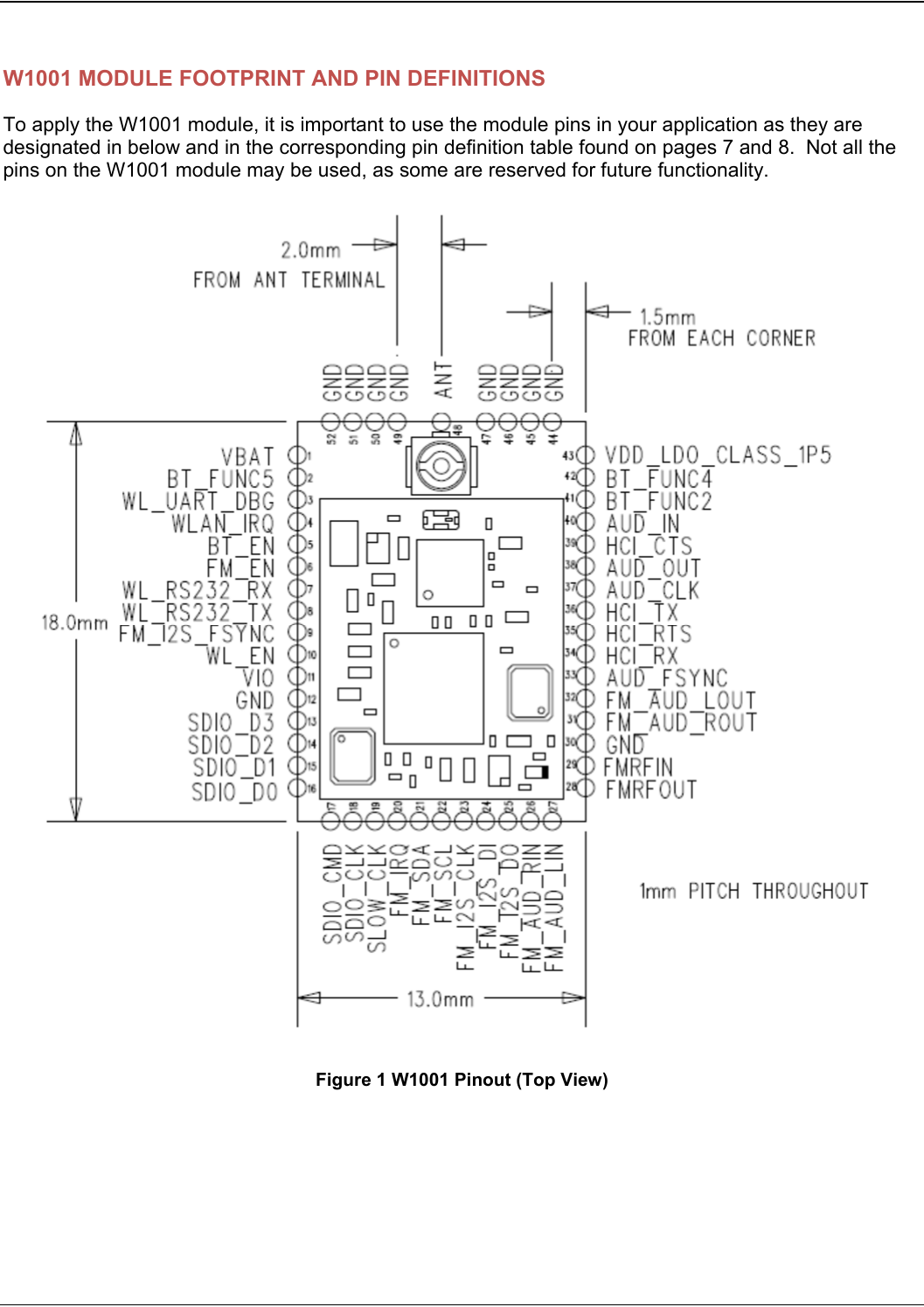
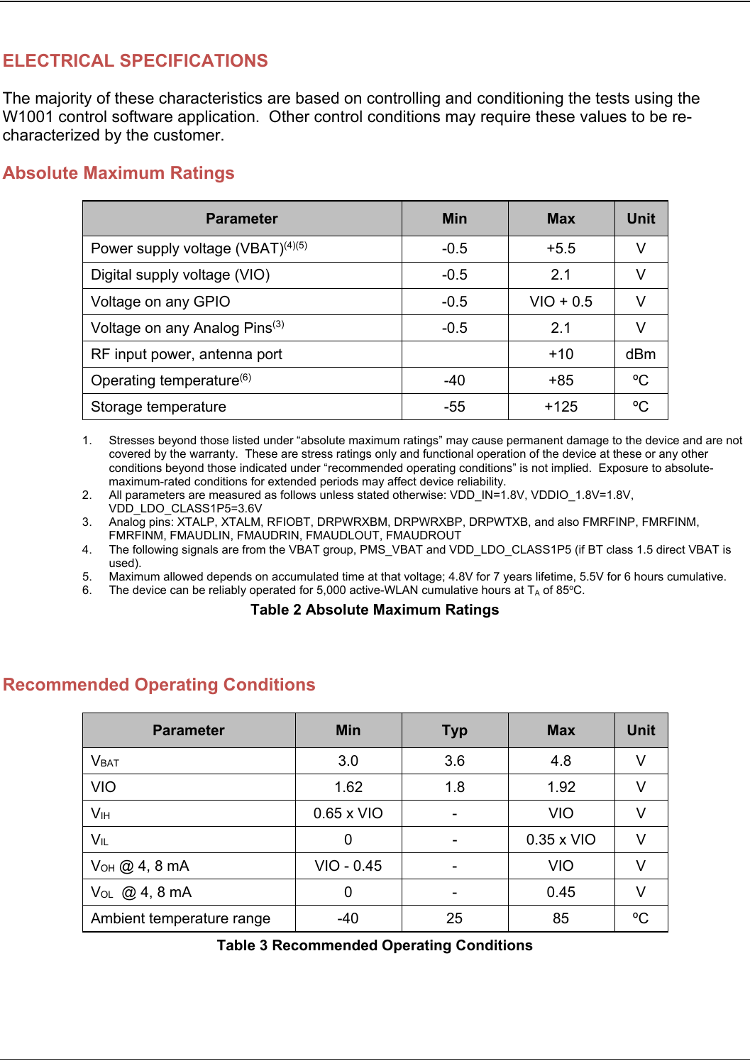
![ModulePin Name I/O Type BufferTypeLogic Level Description 32 FM_AUD_LOUT AO - - NOT SUPPORTED, NO CONNECT33 AUD_FSYNC DIO 4 mA 1.8 VDC PCM I/F34 HCI_RX DI 8 mA 1.8 VDC Bluetooth HCI UART RX (*) 35 HCI_RTS DO 4 mA 1.8 VDC Bluetooth HCI UART RTS (*) 36 HCI_TX DIO 8 mA 1.8 VDC Bluetooth HCI UART TX 37 AUD_CLK DO 4 mA 1.8 VDC PCM I/F (*)38 AUD_OUT DO 4 mA 1.8 VDC PCM I/F (*)39 HCI_CTS DI 4 mA 1.8 VDC Bluetooth HCI UART CTS (*) 40 AUD_IN DI 4 mA 1.8 VDC PCM I/F (*)41 BT_FUNC2 DO 4 mA 1.8 VDC Bluetooth Wakeup / DC2DC Mode (*)42 BT_FUNC4 DO 4 mA 1.8 VDC BT_UARTD (DEBUG) (*) 43 VDD_LDO_CLASS_1P5 NC - - VBAT VOLTAGE PRESENT, NO CONNECT44 GND GND - - Ground45 GND GND - - Ground46 GND GND - - Ground47 GND GND - - Ground48 ANT RF - Antenna terminal for WLAN and Bluetooth (Note [1])49 GND GND - - Ground50 GND GND - - Ground51 GND GND - - Ground52 GND GND - - GroundPI = Power Input PO = Power Output DI = Digital Input (1.8 VDC Logic Level) DO=Digital Output (1.8 VDC Logic Level) AI = Analog Input AO = Analog Output AIO = Analog Input/Output RF = RF Port GND = Ground Note[1]: Antenna terminal presents d.c. short circuit to ground. (*) indicates that pin is capable of bidirectional operation, but is used as the type shown. Table 1 W1001 Module Pin Descriptions All digital I/O signals use 1.8V logic. If the host microcontroller does not support 1.8V logic, then level shifters MUST be used.](https://usermanual.wiki/Thermo-Scientific/W1001/User-Guide-3268237-Page-4.png)