Thermo Scientific W1001 W1001 Module User Manual TF W1001 Manual Rev 1
Thermo Scientific, Inc. W1001 Module TF W1001 Manual Rev 1
User Manual

Integrated Transceiver Modules for WLAN 802.11 b/g/n, Bluetooth,
Bluetooth Low Energy (BLE), and ANT
FEATURES
IEEE 802.11b,g,n,d,e,i compliant
Typical WLAN Transmit Power:
o 20.0dBm, 11 Mbps,CCK (b)
o 14.5dBm, 54 Mbps,OFDM (g)
o 12.5dBm, 65 Mbps,OFDM (n)
Typical WLAN Sensitivity:
o -89dBm, 8% PER, 11 Mbps
o -76dBm, 10% PER, 54 Mbps
o -73dBm, 10% PER, 65 Mbps
Bluetooth 2.1+EDR, Power Class 1.5
Full support for BLE 4.0 and ANT
Miniature footprint: 18 mm x 13 mm
Low height profile: 1.9 mm
U.FL connector for external antenna
Terminal for PCB/Chip antenna feeds
Integrated band-pass filter
Compact design based on Texas
Instruments WL1271L Transceiver
Seamless integration with TI OMAP™
application processors
SDIO Host data path interfaces
Bluetooth Advanced Audio Interfaces
Low power operation mode
RoHS compliant
APPLICATIONS
Security
HVAC Control, Smart Energy
Sensor Networks
Medical
DESCRIPTION
The W1001 module is a high performance 2.4
GHz IEEE 802.11 b/g/n, Bluetooth 2.1+EDR,
and Bluetooth Low Energy (BLE) 4.0 radio in a
cost effective, pre-certified footprint.
The module realizes the necessary PHY/MAC
layers to support WLAN applications in
conjunction with a host processor over a SDIO
interface.
The module also provides a Bluetooth platform
through the HCI transport layer. Both WLAN
and Bluetooth share the same antenna port.

W1001 MODULE FOOTPRINT AND PIN DEFINITIONS
To apply the W1001 module, it is important to use the module pins in your application as they are
designated in below and in the corresponding pin definition table found on pages 7 and 8. Not all the
pins on the W1001 module may be used, as some are reserved for future functionality.
Figure 1 W1001 Pinout (Top View)

PIN DESCRIPTIONS
ModulePin Name I/O
Type
Buffer
Type
Logic
Level Description
1 VBAT PI - - Battery Voltage 3.6 VDC Nominal (3.0-4.8 VDC)
2 BT_FUNC5 DO 4 mA 1.8 VDC HOST_WU (*)
3 WL_UART_DBG DIO 4 mA 1.8 VDC WL_UART_DBG
4 WLAN_IRQ DO 4 mA 1.8 VDC WLAN Interrupt Request
5 BT_EN DI -1.8 VDC Bluetooth Enable
6 FM_EN DI -1.8 VDC NOT SUPPORTED, CONNECT TO GND
7 WL_RS232_RX DI -1.8 VDC WLAN TEST UART RX (*)
8 WL_RS232_TX DO 4 mA 1.8 VDC WLAN TEST UART TX (*)
9 FM_I2S_FSYNC DO 4 mA 1.8 VDC NOT SUPPORTED, NO CONNECT
10 WL_EN DI -1.8 VDC WLAN Enable
11 VIO PI - - POWER SUPPLY FOR 1.8 VDC DIGITAL
DOMAIN
12 GND GND - - Ground
13 SDIO_D3 DIO 8 mA 1.8 VDC SDIO INTERFACE, HOST PULL UP
14 SDIO_D2 DIO 8 mA 1.8 VDC SDIO INTERFACE, HOST PULL UP
15 SDIO_D1 DIO 8 mA 1.8 VDC SDIO INTERFACE, HOST PULL UP
16 SDIO_D0 DIO 8 mA 1.8 VDC SDIO INTERFACE, HOST PULL UP
17 SDIO_CMD DIO 8 mA 1.8 VDC HOST PULL UP
18 SDIO_CLK DI -1.8 VDC HOST PULL UP
19 SLOW_CLK DI -1.8 VDC SLEEP CLOCK (32 kHz)
20 FM_IRQ DO 4 mA 1.8 VDC NOT SUPPORTED, NO CONNECT
21 FM_SDA DO 4 mA 1.8 VDC NOT SUPPORTED, NO CONNECT
22 FM_SCL DO 4 mA 1.8 VDC NOT SUPPORTED, NO CONNECT
23 FM_I2S_CLK DO 4 mA 1.8 VDC NOT SUPPORTED, NO CONNECT
24 FM_I2S_DI DI 4 mA 1.8 VDC NOT SUPPORTED, CONNECT TO GND
25 FM_I2S_DO DO 4 mA 1.8 VDC NOT SUPPORTED, NO CONNECT
26 FM_AUD_RIN AI - - NOT SUPPORTED, CONNECT TO GND
27 FM_AUD_LIN AI - - NOT SUPPORTED, CONNECT TO GND
28 FMRFOUT AO - - NOT SUPPORTED, NO CONNECT
29 FMRFIN AI - - NOT SUPPORTED, CONNECT TO GND
30 GND GND - - Ground
31 FM_AUD_ROUT AO - - NOT SUPPORTED, NO CONNECT
ModulePin Name I/O
Type
Buffer
Type
Logic
Level Description
32 FM_AUD_LOUT AO - - NOT SUPPORTED, NO CONNECT
33 AUD_FSYNC DIO 4 mA 1.8 VDC PCM I/F
34 HCI_RX DI 8 mA 1.8 VDC Bluetooth HCI UART RX (*)
35 HCI_RTS DO 4 mA 1.8 VDC Bluetooth HCI UART RTS (*)
36 HCI_TX DIO 8 mA 1.8 VDC Bluetooth HCI UART TX
37 AUD_CLK DO 4 mA 1.8 VDC PCM I/F (*)
38 AUD_OUT DO 4 mA 1.8 VDC PCM I/F (*)
39 HCI_CTS DI 4 mA 1.8 VDC Bluetooth HCI UART CTS (*)
40 AUD_IN DI 4 mA 1.8 VDC PCM I/F (*)
41 BT_FUNC2 DO 4 mA 1.8 VDC Bluetooth Wakeup / DC2DC Mode (*)
42 BT_FUNC4 DO 4 mA 1.8 VDC BT_UARTD (DEBUG) (*)
43 VDD_LDO_CLASS_1P5 NC - - VBAT VOLTAGE PRESENT, NO CONNECT
44 GND GND - - Ground
45 GND GND - - Ground
46 GND GND - - Ground
47 GND GND - - Ground
48 ANT RF - Antenna terminal for WLAN and Bluetooth (Note
[1])
49 GND GND - - Ground
50 GND GND - - Ground
51 GND GND - - Ground
52 GND GND - - Ground
PI = Power Input PO = Power Output DI = Digital Input (1.8 VDC Logic Level) DO=Digital Output (1.8 VDC Logic Level)
AI = Analog Input AO = Analog Output AIO = Analog Input/Output RF = RF
Port GND = Ground
Note[1]: Antenna terminal presents d.c. short circuit to ground.
(*) indicates that pin is capable of bidirectional operation, but is used as the type shown.
Table 1 W1001 Module Pin Descriptions
All digital I/O signals use 1.8V logic. If the host microcontroller does not support 1.8V
logic, then level shifters MUST be used.
ELECTRICAL SPECIFICATIONS
The majority of these characteristics are based on controlling and conditioning the tests using the
W1001 control software application. Other control conditions may require these values to be re-
characterized by the customer.
Absolute Maximum Ratings
Parameter Min Max Unit
Power supply voltage (VBAT)(4)(5) -0.5 +5.5 V
Digital supply voltage (VIO) -0.5 2.1 V
Voltage on any GPIO -0.5 VIO + 0.5 V
Voltage on any Analog Pins(3) -0.5 2.1 V
RF input power, antenna port +10 dBm
Operating temperature(6) -40 +85 ºC
Storage temperature -55 +125 ºC
1. Stresses beyond those listed under “absolute maximum ratings” may cause permanent damage to the device and are not
covered by the warranty. These are stress ratings only and functional operation of the device at these or any other
conditions beyond those indicated under “recommended operating conditions” is not implied. Exposure to absolute-
maximum-rated conditions for extended periods may affect device reliability.
2. All parameters are measured as follows unless stated otherwise: VDD_IN=1.8V, VDDIO_1.8V=1.8V,
VDD_LDO_CLASS1P5=3.6V
3. Analog pins: XTALP, XTALM, RFIOBT, DRPWRXBM, DRPWRXBP, DRPWTXB, and also FMRFINP, FMRFINM,
FMRFINM, FMAUDLIN, FMAUDRIN, FMAUDLOUT, FMAUDROUT
4. The following signals are from the VBAT group, PMS_VBAT and VDD_LDO_CLASS1P5 (if BT class 1.5 direct VBAT is
used).
5. Maximum allowed depends on accumulated time at that voltage; 4.8V for 7 years lifetime, 5.5V for 6 hours cumulative.
6. The device can be reliably operated for 5,000 active-WLAN cumulative hours at TA of 85oC.
Table 2 Absolute Maximum Ratings
Recommended Operating Conditions
Parameter Min Typ Max Unit
VBAT 3.0 3.6 4.8 V
VIO 1.62 1.8 1.92 V
VIH 0.65 x VIO - VIO V
VIL 0 - 0.35 x VIO V
VOH @ 4, 8 mA VIO - 0.45 - VIO V
VOL @ 4, 8 mA 0 - 0.45 V
Ambient temperature range -40 25 85 ºC
Table 3 Recommended Operating Conditions
General Characteristics
Parameter Min Typ Max Unit
WLAN RF frequency range 2412 2472 MHz
WLAN RF data rate 1
802.11 b/g/n
rates
supported
65 Mbps
BT RF frequency Range 2402 2480 MHz
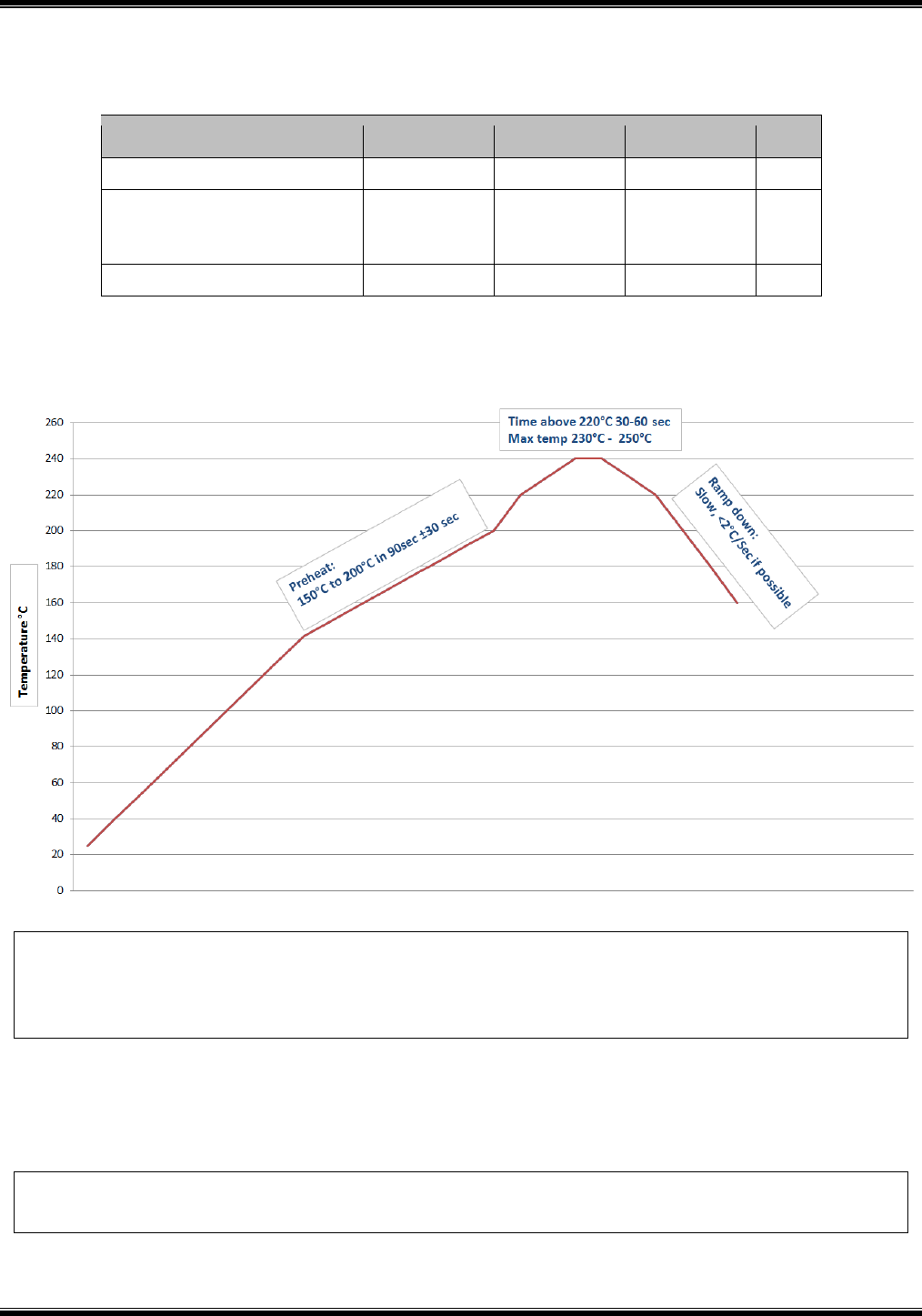
Table 4 General CharacteristicsSoldering Recommendations
Recommended Reflow Profile for Lead Free Solder
Note: The quality of solder joints on the castellations (‘half vias’) where they contact the
host board should meet the appropriate IPC Specification. See IPC-A-610-D Acceptability
of Electronic Assemblies, section 8.2.4 Castellated Terminations.”
Figure 2 Reflow Profile
Repeating Reflow Soldering
Only a single reflow soldering process is encouraged for host boards.

Cleaning
In general, cleaning the populated modules is
strongly discouraged. Residuals under the
module cannot be easily removed with any
cleaning process.
Cleaning with water can lead to capillary
effects where water is absorbed into the gap
between the host board and the module.
The combination of soldering flux residuals
and encapsulated water could lead to short
circuits between neighboring pads. Water
could also damage any stickers or labels.
Cleaning with alcohol or a similar organic
solvent will likely flood soldering flux
residuals into the RF shield, which is not
accessible for post-washing inspection. The
solvent could also damage any stickers or
labels.
Ultrasonic cleaning could damage the
module permanently.
OPTICAL INSPECTION
After soldering the Module to the host board,
consider optical inspection to check the
following:
Proper alignment and centering of the
module over the pads.
Proper solder joints on all pads.
Excessive solder or contacts to neighboring
pads, or vias.
REWORK
The module can be unsoldered from the host
board if the Moisture Sensitivity Level (MSL)
requirements are met as described in this
datasheet.
Never attempt a rework on the module
itself, e.g. replacing individual
components. Such actions will
terminate warranty coverage.
HANDLING AND STORAGE
Handling
The W1001 modules contain a highly sensitive
electronic circuitry. Handling without proper
ESD protection may destroy or damage the
module permanently. ESD protection may
destroy or damage the module permanently.
Moisture Sensitivity Level (MSL)
Per J-STD-020, devices rated as MSL 4 and
not stored in a sealed bag with desiccant pack
should be baked prior to use.
After opening packaging, devices that will be
subjected to reflow must be mounted within 72
hours of factory conditions (<30°C and 60%
RH) or stored at <10% RH.
Bake devices for 48 hours at 125°C.
Storage
Please use this product within 6 months after
receipt. Any product used after 6 months of
receipt needs to have solderability confirmed
before use.
The product shall be stored without opening the
packing under the ambient temperature from 5 to
35deg.C and humidity from 20 to 70%RH.
(Packing materials, in particular, may be
deformed at the temperatures above this range.)
Do not store in salty air or in an environment
with a high concentration of corrosive gas, such
as Cl2, H2S, NH3, SO2, or NOX.
Do not store in direct sunlight.
The product should not be subject to excessive
mechanical shock.

AGENCY CERTIFICATIONS
FCC ID: Z4H-W1001
IC: 9812A-W1001
AGENCY STATEMENTS
Federal Communication Commission Interference Statement
This equipment has been tested and found to comply with the limits for a Class B digital device,
pursuant to Part 15 of the FCC Rules. These limits are designed to provide reasonable protection
against harmful interference in a residential installation. This equipment generates uses and can radiate
radio frequency energy and, if not installed and used in accordance with the instructions, may cause
harmful interference to radio communications. However, there is no guarantee that interference will not
occur in a particular installation. If this equipment does cause harmful interference to radio or television
reception, which can be determined by turning the equipment off and on, the user is encouraged to try
to correct the interference by one of the following measures:
Reorient or relocate the receiving antenna.
Increase the separation between the equipment and receiver.
Connect the equipment into an outlet on a circuit different from that to which the receiver is
connected.
Consult the dealer or an experienced radio/TV technician for help.
This device complies with Part 15 of the FCC Rules. Operation is subject to the following two
conditions: (1) This device may not cause harmful interference, and (2) this device must accept any
interference received, including interference that may cause undesired operation.
FCC CAUTION: Any changes or modifications not expressly approved by the party
responsible for compliance could void the user's authority to operate this equipment.
To comply with FCC and Industry Canada RF exposure limits for general population / uncontrolled
exposure, the antenna(s) used for this transmitter must be installed to provide a separation distance of
at least 20cm from all persons and must not be operating in conjunction with any other antenna or
transmitter, except in accordance with FCC multi-transmitter product procedures.

Industry Canada Statements
This Device complies with Industry Canada License-exempt RSS standard(s). Operation is subject to
the following two conditions: 1) this device may not cause interference, and 2) this device must accept
any interference, including interference that may cause undesired operation of the device.
Under Industry Canada regulations, this radio transmitter may only operate using an antenna of a type
and maximum (or lesser) gain approved for the transmitter by Industry Canada. To reduce potential
radio interference to other users, the antenna type and its gain should be so chosen that the equivalent
isotropically radiated power (e.i.r.p.) is not more than that necessary for successful communication.
This device has been designed to operate with the antenna(s) listed below, and having a maximum
gain of 4.3 dBi (LSR Dipole) and -0.6dBi (Ethertronics Presetta). Antennas not included in this list or
having a gain greater than 4.3 dBi and -0.6dBi are strictly prohibited for use with this device. The
required antenna impedance is 50 ohms.
List of all Antennas Acceptable for use with the Transmitter
1) LS Research 001-0001 center-fed dipole antenna and LS Research 080-0001 U.FL to Reverse
Polarity SMA connector cable.
2) Ethertronics Presetta 1000423 and Johnson Emerson U.FL. to U.FL coaxial cable 415-0088-150.
3) LS Research 001-0014 2.4 GHz FlexPIFA Antenna w/U.FL Cable.
Cet appareil est conforme avec Industrie Canada, exempts de licence standard RSS (s). Son
fonctionnement est soumis aux deux conditions suivantes: 1) ce dispositif ne peut pas causer
d'interférences, et 2) ce dispositif doit accepter toute interférence, y compris les interférences qui
peuvent causer un mauvais fonctionnement de l'appareil.
En vertu des règlements d'Industrie Canada, cet émetteur de radio ne peut fonctionner en utilisant une
antenne d'un type et maximale (ou moins) Gain approuvé pour l'émetteur par Industrie Canada. Pour
réduire les interférences radio potentielles pour les autres utilisateurs, le type d'antenne et son gain
doivent être choisis afin que la puissance isotrope rayonnée équivalente (PIRE) ne dépasse pas ce qui
est nécessaire pour une communication réussie.
Cet appareil a été conçu pour fonctionner avec l'antenne (s) ci-dessous, et ayant un gain maximum de
4,3 dBi (LSR dipôle) et -0.6dBi (Ethertronics Presetta). Antennes pas inclus danscette liste ou
d'avoir un gain supérieur à 4,3 dBi et -0.6dBi sont strictement interdites pour l'utilisation avec cet
appareil. L'impédance d'antenne requise est de 50 ohms.
Liste de toutes les antennes acceptables pour une utilisation avec l'émetteur
1) LS Research 001-0001 alimenté par le centre antenne dipôle et LS Research 080-0001
U.FL d'inversion de polarité du câble connecteur SMA.
2) Ethertronics Presetta 1000423 et Johnson Emerson U.FL d'un câble coaxial U.FL 415-0088-150.
3) LS Research 001-0014 2,4 GHz antenne FlexPIFA w/U.FL Cable.

OEM RESPONSIBILITIES TO COMPLY WITH FCC AND INDUSTRY CANADA
REGULATIONS
The W1001 Module has been certified for integration into products only by OEM integrators under the
following condition:
To comply with FCC and Industry Canada RF exposure limits for general population / uncontrolled
exposure, the antenna(s) used for this transmitter must be installed to provide a separation distance of
at least 20cm from all persons and must not be operating in conjunction with any other antenna or
transmitter, except in accordance with FCC multi-transmitter product procedures.
However, the OEM integrator is still responsible for testing their end-product for any additional
compliance requirements required with this module installed (for example, digital device emissions, PC
peripheral requirements, etc.).
IMPORTANT NOTE: In the event that these conditions cannot be met (for certain
configurations or co-location with another transmitter), then the FCC and Industry Canada
authorizations are no longer considered valid and the FCC ID and IC Certification Number
cannot be used on the final product. In these circumstances, the OEM integrator will be
responsible for re-evaluating the end product (including the transmitter) and obtaining a
separate FCC and Industry Canada authorization.
Le module de W1001 a été certifié pour l'intégration dans des produits uniquement par des
intégrateurs OEM dans les conditions suivante:
Pour se conformer aux limites d'exposition aux RF de la FCC et d'Industrie Canada pour la population
générale / exposition non contrôlée, l'antenne(s) utilisée pour ce transmetteur doit être installé pour
fournir une distance de séparation d'au moins 20cm de toutes les personnes et fonctionnant
conjointement avec une autre antenne ou émetteur, sauf en conformité avec les procédures de
produits multi- émetteur FCC.
Toutefois, l'intégrateur OEM est toujours responsable de tester leur produit final pour toutes les
exigences de conformité supplémentaires requis avec ce module installé (par exemple, les émissions
appareil numérique, les exigences de périphériques PC, etc.)
NOTE IMPORTANTE: Dans le cas où ces conditions ne peuvent être satisfaites (pour
certaines configurations ou de co-implantation avec un autre émetteur), puis la FCC et
Industrie autorisations Canada ne sont plus considérés comme valides et l'ID de la FCC et
IC numéro de certification ne peut pas être utilisé sur la produit final. Dans ces
circonstances, l'intégrateur OEM sera chargé de réévaluer le produit final (y compris
l'émetteur) et l'obtention d'un distincte de la FCC et Industrie Canada l'autorisation.

OEM LABELING REQUIREMENTS FOR END-PRODUCT
The W1001 module is labeled with its own FCC ID and IC Certification Number. The FCC ID and IC
certification numbers are not visible when the module is installed inside another device, as such the
end device into which the module is installed must display a label referring to the enclosed module.
The final end product must be labeled in a visible area with the following:
“Contains Transmitter Module FCC ID: Z4H-W1001”
“Contains Transmitter Module IC: 9812A-W1001”
or
“Contains FCC ID: Z4H-W1001”
“Contains IC: 9812A-W1001”
The OEM of the W1001 Module must only use the approved antenna(s) listed above, which have been
certified with this module.
Le module de W1001 est étiqueté avec son propre ID de la FCC et IC numéro de certification. L'ID de
la FCC et IC numéros de certification ne sont pas visibles lorsque le module est installé à
l'intérieur d'un autre appareil, comme par exemple le terminal dans lequel le module est installé
doit afficher une etiquette faisant référence au module ci-joint. Le produit final doit être étiqueté dans un
endroit visible par le suivant:
“Contient Module émetteur FCC ID: Z4H-W1001"
“Contient Module émetteur IC: 9812A-W1001"
ou
“Contient FCC ID: Z4H-W1001"
“Contient IC: 9812A-W1001"
L’OEM du module W1001 ne doit utiliser l'antenne approuvée (s) ci-dessus, qui ont été certifiés avec
ce module.

OEM END PRODUCT USER MANUAL STATEMENTS
The OEM integrator should not provide information to the end user regarding how to install or remove
this RF module or change RF related parameters in the user manual of the end product.
The user manual for the end product must include the following information in a prominent
location:
To comply with FCC and Industry Canada RF exposure limits for general population / uncontrolled
exposure, the antenna(s) used for this transmitter must be installed to provide a separation distance of
at least 20cm from all persons and must not be operating in conjunction with any other antenna or
transmitter, except in accordance with FCC multi-transmitter product procedures.
Other user manual statements may apply.
L'intégrateur OEM ne devrait pas fournir des informations à l'utilisateur final en ce qui concerne la façon
d'installer ou de retirer ce module RF ou modifier les paramètres RF connexes dans le manuel
utilisateur du produit final.
Le manuel d'utilisation pour le produit final doit comporter les informations suivantes dans
unendroit bien en vue:
Pour se conformer aux limites d'exposition aux RF de la FCC et d'Industrie Canada pour la population
générale / exposition non contrôlée, l'antenne(s) utilisée pour ce transmetteur doit être installé pour
fournir une distance de séparation d'au moins 20cm de toutes les personnes et fonctionnant
conjointement avec une autre antenne ou émetteur, sauf en conformité avec les procédures de
produits multi- émetteur FCC.
Autres déclarations manuel de l'utilisateur peuvent s'appliquer.
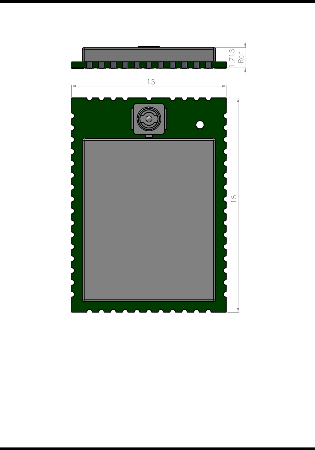
MECHANICAL DATA
Figure 3 Module Mechanical Dimensions (Maximum Module Height = 1.9 mm)

Figure 4 W1001 Recommended PCB Footprint (Top View)