Thomson Broadcast and Multimedia 8BUSD2500B 25 watt digital transmitter system User Manual 33 0040 SD2500 manual
Thomson Broadcast & Multimedia, Inc. 25 watt digital transmitter system 33 0040 SD2500 manual
manual
38
SD2500 TECHNICAL MANUAL
COMWAVE DIVISION
All information contained in this document is confidential and proprietary to THOMCAST and shall not be disclosed without the prior written permission of THOMCAST.
CREATED: KAS...................................................................12/9/99 CHECKED: DMW ................................................................12/9/99 RELEASED: PRC..................................................................12/9/99
Document #: DOC33-0040
REV: DEC.09.99
5. Close the 4-pack master box and seal
the top seam with 2” clear box tape,
using three layers to assure strength.
Then put 4 pieces of fiberglass
strapping tape over the edges. Clearly
mark the RA number on the outside of
the box before shipping.
Figure 21: Power amplifier segments ready to ship.

37
SD2500 TECHNICAL MANUAL
COMWAVE DIVISION
All information contained in this document is confidential and proprietary to THOMCAST and shall not be disclosed without the prior written permission of THOMCAST.
CREATED: KAS...................................................................12/9/99 CHECKED: DMW ................................................................12/9/99 RELEASED: PRC..................................................................12/9/99
Document #: DOC33-0040
REV: DEC.09.99
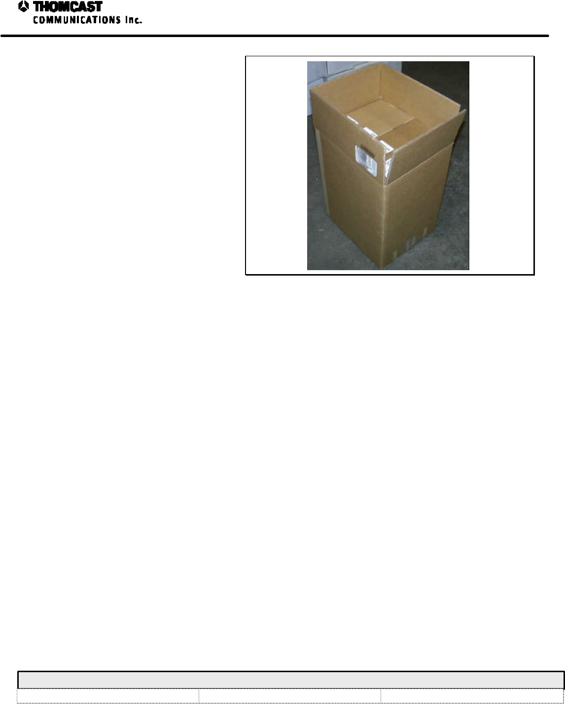
RETURN PACKAGING OF THE POWER AMPLIFER SEGMENT
1. Start with an empty power amplifier
segment box, shown in Figure19. If
you don’t have one please inform
Comwave customer service when you
contact them for a return authorization
(RA) number, which you MUST do
prior to returning ANY equipment.
2. Place the power amplifier segment into
the box, as shown in Figure20. The
heatsink should always face up and the
connectors on the rear of the power
amp segment rest against the soft gray
foam for protection.
Figure 19: Empty power amplifier segment box.
HEATSINK
REAR
Figure 20: Boxed power amplifier segment.
3. Fold the edges of the inner box in and
close.
4. Place the inner box into the 4-pack
master (outer box), being sure to
include three empty power amplifier
boxes for a secure fit, as shown in
Figure21. The power amplifier
segments are generally packed 4 per
master box and shipped. When
returning segment(s) please pack them
the same way, ALL boxes will be
returned to you. If you need to
assemble a master box, use 2” clear
box tape over the bottom seam, using
three layers to assure strength. Then
put 4 pieces of fiberglass strapping
tape over the edges.
36
SD2500 TECHNICAL MANUAL
COMWAVE DIVISION
All information contained in this document is confidential and proprietary to THOMCAST and shall not be disclosed without the prior written permission of THOMCAST.
CREATED: KAS...................................................................12/9/99 CHECKED: DMW ................................................................12/9/99 RELEASED: PRC..................................................................12/9/99
Document #: DOC33-0040
REV: DEC.09.99
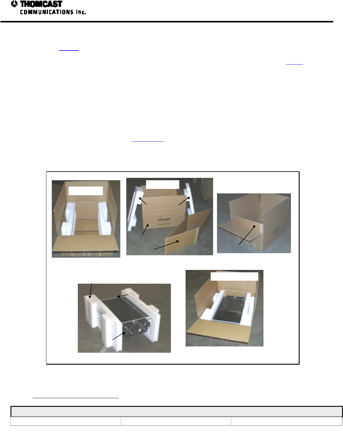
RETURN PACKAGING
Below is a pictorial view of the following steps.
1) Begin with an empty Thomcast box, if you don’t have one please inform customer service when you contact
them for a return authorization (RA) number, which you MUST do prior to returning ANY equipment. NOTE:
A box consists of 4 parts, one cardboard box, one cardboard tube, and two polyethylene endcaps.
a) To assemble a flattened box put three23 layers of 2” clear box tape over the bottom seam, then position four
pieces of fiberglass strapping tape over the edges.
2) Put the cardboard tube in the box.
3) Place the polyethylene endcaps against the sides of the equipment. NOTE the front panel fits snuggly into a
slotted opening in the endcap.
4) Put the chassis in the box.
5) Close the box and seal the top seam with three layers of 2” clear box tape, then position four pieces of fiberglass
strapping tape over the edges.
6) Affix a shipping label to the box see DOC20-0001, preceding this document, for shipping address.
7) Mark the RA number on the outside of the box before shipping. If the RA number is not clearly visible
Thomcast cannot be held responsible for delays in repair and return time.
EMPTY BOX.
CARDBOARD BOX
CARDBOARD TUBE
POLYETHYLENE ENDCAPS
BOX PARTS.
CARDBOARD TUBE
PLACING THE CARDBOARD TUBE.
REAR
FRONT
SLOTTED OPENING
PLACING THE ENDCAPS. PACKED CHASSIS.
Figure 18: Equipment packing.
23 Using several layers of tape assures the strength of the box.
35
SD2500 TECHNICAL MANUAL
COMWAVE DIVISION
All information contained in this document is confidential and proprietary to THOMCAST and shall not be disclosed without the prior written permission of THOMCAST.
CREATED: KAS...................................................................12/9/99 CHECKED: DMW ................................................................12/9/99 RELEASED: PRC..................................................................12/9/99
Document #: DOC33-0040
REV: DEC.09.99
CUSTOMER SERVICE
DOC20-0001
CONTACT INFORMATION
DURING BUSINESS HOURS
Inquiries may be directed to Thomcast Communications, Comwave Division during business hours, 8 am to 5 pm
Monday through Friday. When the automated attendant answers you will be given the option of dialing your party
direct or speaking with the operator.
AFTER BUSINESS HOURS
If you need emergency assistance due to equipment shutdown or malfunction, customer support personnel are
available 24 hours a day. Call Thomcast at one of the numbers listed below; when the automated attendant answers
press 6, leave your name, company name, phone number, equipment model number(s), and a brief description of the
problem you’re encountering. When you hang up the system will automatically page the on-call technician who will
then return your call in a timely manner. You can listen to the message prompt for other options as well, however,
for emergency assistance you MUST use option 6.
Thomcast Communications, Comwave Division
Crestwood Industrial Park, 395 Oakhill Road
Mountaintop, PA 18707
1-800-266-9283 USA & Canada
1-570-474-6751 International21 & USA
(Please note, as of 12/98, our area code changed from 717 to 570)
1-570-474-5469 FAX
(Please note, as of 12/98, our area code changed from 717 to 570)
COMMENTS/SUGGESTIONS
Please forward comments regarding documentation content and/or layout, or suggestions to improve Thomcast
publications to ksimeone@thomcastcom.com.
EQUIPMENT RETURNS
If the equipment requires return for factory service, please follow the guidelines listed. Thomcast cannot be held
responsible for damaged equipment received due to improper packing; contact Thomcast with any questions or
concerns.
1. Contact Thomcast: Call Thomcast to report the problem and to obtain a “Return Authorization”
number22 (RA). This enables accurate tracking and identity of returned equipment for prompt and efficient
service.
2. Obtain packaging materials: Use original boxes and packing materials when returning any equipment. This will
safeguard against most in-transit damages. If original boxes and packing materials are not available, contact
Thomcast to obtain replacement materials prior to shipping, they are provided at a nominal cost.
4. Pack equipment: Use original packing materials and directions provided. Most equipment is packed in a box
within another box; this varies with each product. Double boxing provides maximum protection.
Caution: Do not pack equipment using “PEANUTS” as filler it does NOT provide sufficient protection
during shipping. Rough handling by the carrier may cause permanent damage to the equipment.
Thomcast cannot be held responsible for damaged equipment received due to improper packing.
21 International calls must dial the country code before the phone number, i.e. 001-570-474-6751.
22 If you do not obtain an RA number prior to returning equipment Thomcast cannot be held responsible for delays in repair and return time.

34
SD2500 TECHNICAL MANUAL
COMWAVE DIVISION
All information contained in this document is confidential and proprietary to THOMCAST and shall not be disclosed without the prior written permission of THOMCAST.
CREATED: KAS...................................................................12/9/99 CHECKED: DMW ................................................................12/9/99 RELEASED: PRC..................................................................12/9/99
Document #: DOC33-0040
REV: DEC.09.99
POWER AMPLIFIER SEGMENT SPECIFICATIONS
Table 3: DOC19-0014, REV D.
PARAMETER SPECIFICATION
Primary Voltage 48 VDC
Primary Current 4.9 A
Secondary Voltage 10 ±0.5 VDC
Secondary Current 400 mA
Communication Port RS-232 and RS-485
Input Power
Digital
Analog 12.0 dBm
17.5 dBm (@ POut1dB)
Output Power
Digital
Analog
41.5 dBm
47.0 dBm (@ POut1dB)
DC Connector Floating Molex p/n 15-06-0141
Impedance / RF Connector 50 O / Blindmate
Operating Temperature 0° to 50° C
Dimensions 10.3” H x 2.1” W x 17.1” D
26.16 cm H x 5.33 cm W x 43.43 cm D
Approximate Weight20 10 lbs (4 Kg)
20 Weight doesn’t include shipping material.
33
SD2500 TECHNICAL MANUAL
COMWAVE DIVISION
All information contained in this document is confidential and proprietary to THOMCAST and shall not be disclosed without the prior written permission of THOMCAST.
CREATED: KAS...................................................................12/9/99 CHECKED: DMW ................................................................12/9/99 RELEASED: PRC..................................................................12/9/99
Document #: DOC33-0040
REV: DEC.09.99
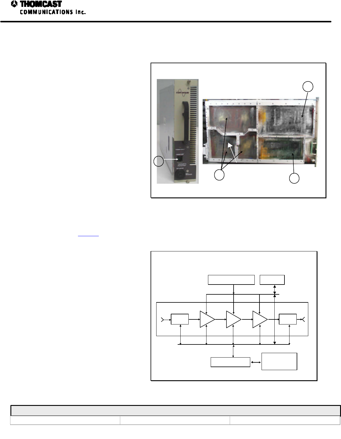
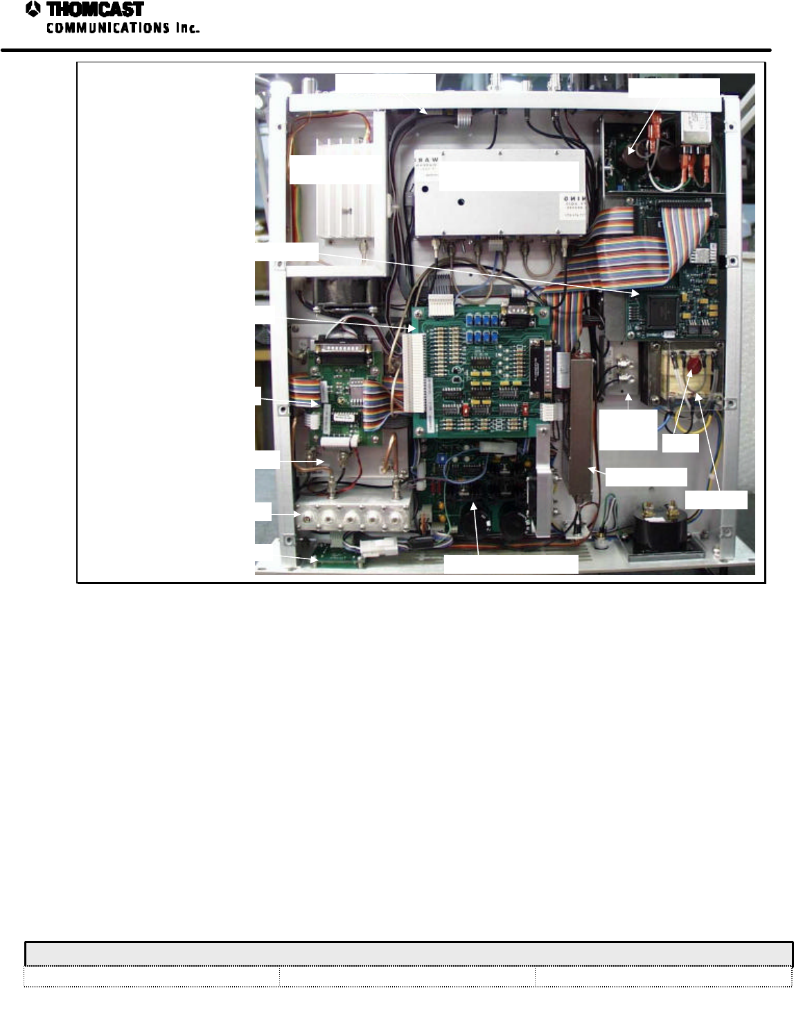
POWER AMPLIFIER SEGMENT THEORY OF OPERATION
DOC14-0008
The power amplifier segments of the high
power single channel transmitter series or
broadband booster series use the latest
technology in power FET’s. The transistors
provide high output power, as well as more
linearity and higher efficiency.
Mechanically, the power amplifier segments
have a plug-in architecture that allows hot
replacement. In addition to hot
replacement, the architecture of the
amplifier enables flexibility to tailor the
system to higher output power levels and
can be easily upgraded.
The power amplifier segment consists of a
microwave amplifier2, control board1, DC to
DC converter3, and a front panel. A
microcontroller system, located on the
control board, supervises and controls the
power amplifier segment in each of its
functions. The DC to DC converter reduces
48 V
DC front-end power supply input to the
nominal amplifier voltage of 10.5 V. The
front panel displays the status of the
amplifier segment and interfaces the control
board to a computer by means of a serial
RS-232 port4. See Figure48 for numerical
references.
1
2
3
FRONT VIEW
SIDE VIEW
4
Figure 16: Power amplifier segment.
OPERATION
The amplifier segment is equipped with a
key lock switch on the front panel to retain
it in place. When pushing-in or pulling-out
the Segment, turn the key lock switch to the
OFF position. After plugging the amplifier
segment into the sub-rack and tightening
the front panel thumbscrews, turn the key-
lock switch to the ON position. The 10
V
DC
secondary power supply will start up
the control board, which applies a negative
voltage to the gates of the FET’s and turns
the DC to DC converter on. It also adjusts
the transistor’s current and releases the
input signal to the microwave amplifier.
The airflow passes through the heatsink
from the front to the rear of the sub-rack.
The airflow loss to the other power
amplifier segments during hot replacement
is negligible.
POWER AMPLIFIER SEGMENT BLOCK DIAGRAM
Microwave Amplifier
Rear Panel
Connector
DC to DC Converter
Control Panel
Front Panel
Connector & Key
Lock Switch
Document #: DOC15-0013 REV: C, ECO #: 98-116
Created by: KAS 9/15/98
Checked by: DMW 9/18/98
Released by: PRC 10/29/98
Figure 17 : DOC15-0013 power amplifier segment block diagram.
32
SD2500 TECHNICAL MANUAL
COMWAVE DIVISION
All information contained in this document is confidential and proprietary to THOMCAST and shall not be disclosed without the prior written permission of THOMCAST.
CREATED: KAS...................................................................12/9/99 CHECKED: DMW ................................................................12/9/99 RELEASED: PRC..................................................................12/9/99
Document #: DOC33-0040
REV: DEC.09.99
SD-SERIES FREQUENCY FIXED DIGITAL DRIVER (2RU)
SPECIFICATIONS18
DOC19-0008
Parameter Specification Notes / Test Conditions
Average Output Power 1.25 Watts @ maximum drive level 223-1 PN data sequence (at transmitter output)
IF Input Frequency 44 MHz Other frequency options available
Impedance/Connector
Input
Output 75 Ω/BNC-female
50 Ω/N-female
Average Input Power -15 dBm ± 0.5 dB 223-1 PN data sequence (at transmitter output)
Output Frequency 2000 - 2700 MHz In select bands
Frequency Stability ≤ ±500 Hz
≤ ±1 Hz (Optional GPS)
SSB Phase Noise
Direct measurement of microwave LO = -80 dBc/Hz @ 10 KHz offset
= -110 dBc/Hz @ 10 KHz offset Optional
Standard (recommended for digital transmission)
Power Requirement 117/230 V
AC ±10%; 50/60 Hz
(=150 VA)
Operating Temperature 0°C to +50°CFrequency stability and equipment functionality
guaranteed
Specified Temperature Range 13° to +33°CAll Specified parameters guaranteed
Relative Humidity 95% non-condensing
Hum and Noise =-60 dBc
Dimensions 3.5” H x 19” W x 17” D
8.89cm H x 48.26cm W x 43.18cm D
Approximate Shipping Weight19 17.5 lb (7.93kg)
18 All factory test measurements made at approximately 23° C.
19 Shipping weight includes the transmitter and shipping material only. Digital modulators are typically shipped directly from the manufacturer.

DRAWN:
RELEASED:
CHECKED:
DWG. NUMBER:
TITLE:
REV: A
DOC15-0067
Block Diagram, SD Series Driver
KAS / 12-6-99
PRC / 12-7-99
DMW / 12-7-99 Scale:
none Sheet
1of 1
COMWAVE DIVISION
REFL
ENVELOPE
DETECTOR
12-027
FWD
EXTERNAL
COUPLER
IF IN
-15 dBm
05-037
BANDPASS FILTER
J1
J2
J1
J3 J4
J5 J6
J7 J1
J2
IPA
RF OUT
IF LINEAR
PROCESSOR
05-073
J2
J1
J1
J5
J4
J3
J2
1 WATT
TERMINATIONS
SYNTHESIZER - OEM
FREQ REF IN
7 dB typical
04-128
09-067
ECO #
NAME/DATE
DescriptionREV
2 dB
AMP 1 AMP 2
-2 dB 22 dB 24 dB
-3 dB
8 dB
10 dBm
1. SD2500 ≈ 19 dBm
2. SD5000 ≈ 22 dBm
3. SD10000 ≈ 25 dBm
RF
PRECORRECTOR
04-302
1. 11 dBm ±2dB
2. 14 dBm ±2dB
3. 17 dBm ±2dB
04-292
1. -10 dBm ±2dB
2. -10 dBm ±2dB
3. -7 dBm ±2dB
-19 dBm ±2dB
-22 dBm ±2dB
-17 dBm ±2dB
0 dBm ±2dB
0 dBm ±2dB
10 dB
6 dB (SD10000 only)
3 dB
(SD2500 only)
14 dBm ±2dB
J6
31
SD2500 TECHNICAL MANUAL
COMWAVE DIVISION
All information contained in this document is confidential and proprietary to THOMCAST and shall not be disclosed without the prior written permission of THOMCAST.
CREATED: KAS...................................................................12/9/99 CHECKED: DMW ................................................................12/9/99 RELEASED: PRC..................................................................12/9/99
Document #: DOC33-0040
REV: DEC.09.99
IF Linear Processor 05-073 (top)
RF Precorrector 04-302 (bottom)
Final Amplifier
Module 04-292
Bandpass filter 05-037
Display board 33-207
RS-485 Board 33-284 OEM Power Supply
Microcontroller Board 34-011
Envelope
Detector
12-027 MOV
OEM Synthesizer
Mother Board 35-081(bottom)
Transition Board 33-420 (top)
Diagnostic Board 33-426 (top)
Mixer/Driver Module 04-128 (bottom)
Transformer
Figure 15: Driver layout.

30
SD2500 TECHNICAL MANUAL
COMWAVE DIVISION
All information contained in this document is confidential and proprietary to THOMCAST and shall not be disclosed without the prior written permission of THOMCAST.
CREATED: KAS...................................................................12/9/99 CHECKED: DMW ................................................................12/9/99 RELEASED: PRC..................................................................12/9/99
Document #: DOC33-0040
REV: DEC.09.99
12 3
1234
56 7 89
FRONT PANEL
REAR PANEL
Figure 14: Driver front and rear panels.

29
SD2500 TECHNICAL MANUAL
COMWAVE DIVISION
All information contained in this document is confidential and proprietary to THOMCAST and shall not be disclosed without the prior written permission of THOMCAST.
CREATED: KAS...................................................................12/9/99 CHECKED: DMW ................................................................12/9/99 RELEASED: PRC..................................................................12/9/99
Document #: DOC33-0040
REV: DEC.09.99
The following status monitoring RED LED’s remain OFF during normal operation. When a failure is detected, the
appropriate LED will illuminate RED. Controlled automatic transmitter shut down is a function of failure severity.
Presence of a RED status LED with normal meter readings and/or normal transmitter operation indicates an out of
tolerance condition with that circuit.
TEMPERATURE: Illuminates RED when internal chassis temperature exceeds 140° Fahrenheit
(60° Celsius). Transmitter shut down occurs. Allow transmitter to cool. Transmitter reset can be
attempted by rotating the front panel function switch to STANDBY.
LO LEVEL: Illuminates RED when the local oscillator loses phase lock. Transmitter shut down
occurs.
DRIVER: Illuminates RED to indicate a failure or an out of tolerance condition with the driver
module. Transmitter usually operates at reduced output power.
FINAL: Illuminates RED to indicate a failure or an out of tolerance condition with the
intermediate power module. Transmitter usually operates at reduced output power.
+11 VDC: Illuminates RED when a failure in the + 11 volt DC main switching power supply or an
out of tolerance condition has been detected by the diagnostic and monitoring circuitry.
-12 VDC:Illuminates RED when a failure in the -12 V
DC gate bias/interlock has been detected.
REAR PANEL
1. RF OUT: RF output connector (Female N type).
2. GRILL: Air outlet vent for cooling.
3. J2: Female 25 pin D-Sub connector for diagnostics monitoring.
4. ACCESS HOLES: For three phone jack connectors and a termination switch from the RS 485 Board used for
communication to ComView Network.
5. J1: Female nine pin D-Sub connector for system monitoring and control.
6. INPUT CONNECTORS (FEMALE BNC’S):
IF IN: Input signal from modulator.
LO IN: Input signal provided by an external source. (ONLY USED IN AGILE TRANSMITTER)
FREQ REF: Input signal from an external frequency reference source.
FWD PWR IN: RF sample from an external coupler.
REFL PWR IN: RF sample from an external coupler.
7. FAN: A rear mounted DC Fan provides switching power supply cooling.
8. FUSE: Main line fuse location (2 amperes).
9. AC INPUT: AC Line input power cord connector.

28
SD2500 TECHNICAL MANUAL
COMWAVE DIVISION
All information contained in this document is confidential and proprietary to THOMCAST and shall not be disclosed without the prior written permission of THOMCAST.
CREATED: KAS...................................................................12/9/99 CHECKED: DMW ................................................................12/9/99 RELEASED: PRC..................................................................12/9/99
Document #: DOC33-0040
REV: DEC.09.99
DIGITAL DRIVER THEORY OF OPERATION
DOC14-0035
The digital driver transmitter receives a digitized intermediate frequency signal typically at -15 dBm, which is
upconverted to an S-band frequency. The transmitter is capable of providing an output of 1.25 W average power. Refer
to the block diagram for the RF signal path.
The IF signal being received is sent to an IF linear processor pre-correcting for frequency response, group delay, and
detection of IF presence. The IF linear processor output is applied to a mixer/amplifier module where it is mixed with a
microwave local oscillator. A bandpass filter follows the mixer to prevent out-of-band products from being amplified
and transmitted. The filtered mixer/amplifier output drives the first intermediate power amplifier. Then a microwave
precorrector module introduces precorrection to reduce amplitude distortions of the power amplifier. It contains an ALC
circuit for maintaining 100% output power over a +2 dB gain variation. Both precorrection and ALC can be separately
turned off by individual switch controls located on the module exterior. Two more stages of amplification assure the
correct level for the final intermediate power amplifier.
The intermediate power amplifier is a broad band, fixed gain linear amplifier that does not require any tuning. An
external coupler provides a metering sample to an envelope detector for forward and reflected powers through 3 dB
isolation attenuators. The average output power is dependent on the drive level needed by the power amplifier array to
achieve rated power.
FRONT AND REAR PANEL DESCRIPTIONS
Refer to the Figure below for numerical references.
FRONT PANEL
1. METER: Provides a visual indication of transmitter status and performance of +11 V
DC switching power
supply, peak forward power, or reflected power. The meter is calibrated to display relative measurements. The
four-position rotary selector switch controls meter function.
2. FUNCTION SWITCH: A four position, user selectable, rotary switch that controls front panel meter
monitoring. The following parameters are selectable for monitoring by the function switch.
STANDBY: Disables transmitting. Power remains applied to all circuits, except the microwave
amplifier modules. Meter will read approximately 0 %.
+ 11 V PS: Provides status of main switching power supply. Meter reads 100 % indicating proper
switching power supply voltage.
REFL PWR: Relative reflected power measurement. Readings of less than 10 % are typical.
FWD PWR: Relative forward output power measurement. 100 % meter reading confirms correct
output power.
3. LED’s: Status monitoring LED’s which provide visual indication of operating parameters and internal
diagnostics. The following status monitoring LED’s illuminate GREEN during normal operation. Absence of
an LED indicates missing signal or parameter that results in a controlled automatic transmitter shut down.
IN SIGNAL: Illuminates GREEN when IF is present or when the bypass switch on the
motherboard is in bypass.
INTERLOCK: Illuminates GREEN when Interlock Logic conditions are satisfied. Interlock
Logic conditions are satisfied when all Microwave Amplifier Modules have -12 V gate bias.

27
SD2500 TECHNICAL MANUAL
COMWAVE DIVISION
All information contained in this document is confidential and proprietary to THOMCAST and shall not be disclosed without the prior written permission of THOMCAST.
CREATED: KAS...................................................................12/9/99 CHECKED: DMW ................................................................12/9/99 RELEASED: PRC..................................................................12/9/99
Document #: DOC33-0040
REV: DEC.09.99
MONTHLY MAINTENANCE RECORD17
DOC18-0006
Analog MeteringDate Channel
FWD REFL +11V PS
Failure LED’s Comments
17 You are encouraged to make copies of this document for future use. Recording the meter readings on a monthly basis assists Thomcast
personnel when problems arise.

26
SD2500 TECHNICAL MANUAL
COMWAVE DIVISION
All information contained in this document is confidential and proprietary to THOMCAST and shall not be disclosed without the prior written permission of THOMCAST.
CREATED: KAS...................................................................12/9/99 CHECKED: DMW ................................................................12/9/99 RELEASED: PRC..................................................................12/9/99
Document #: DOC33-0040
REV: DEC.09.99
HEATSINK
Figure 12: Power amplifier segment
heatsink.
POWER AMPLIFIER SEGMENTS:
Pull each power amplifier segment one at a time from the front
of the rack and vacuum the heatsinks. Due to the hot
replacement feature, if one segment is removed at a time, the
transmitter does not need to be turned off. Plug the segment
back in after cleaning.
• NOTE: Be sure not to bend or damage the fins of the
heatsinks during cleaning.
POWER SUPPLY:
Remove the blanking panel from the rear of
the rack and clean any debris found on the
power supply located behind the driver.
Replace the blanking panel after cleaning.
EXHAUST FANS:
Clean the exhaust fans attached to the rear
door of the rack, removing the fan guards if
necessary. The RF connection will need to
be removed before the door can be opened.
Note: The number of fans is dependent
upon the transmitter configuration.
Blanking panel
Exhaust fans
Figure 13: Blanking panel & exhaust fans.

25
SD2500 TECHNICAL MANUAL
COMWAVE DIVISION
All information contained in this document is confidential and proprietary to THOMCAST and shall not be disclosed without the prior written permission of THOMCAST.
CREATED: KAS...................................................................12/9/99 CHECKED: DMW ................................................................12/9/99 RELEASED: PRC..................................................................12/9/99
Document #: DOC33-0040
REV: DEC.09.99
MAINTENANCE
DOC18-0012
COMWAVE products have been carefully designed to be maintenance free. Only periodic inspection and cleaning
is necessary.
INSPECTIONS
1. Periodically inspect cooling fans on the rear door of the rack and the heatsinks of the power amplifier segments
for heavy accumulations of dirt and/or insects. Heavy accumulation of foreign debris impedes cooling
effectiveness and could lead to premature failure. Should any debris be detected, shut down the transmitter and
follow the cleaning instructions to remove debris from transmitter.
• NOTE: The agile transmitter will automatically recover the channel of the transmitter that is
being cleaned.
2. Record analog meter readings of each driver on a monthly basis. This establishes a performance historical
database. These entries can identify degraded performance before it becomes a hard failure.
3. After performing routine maintenance, be sure to check the tightness of all cable connections and especially the
integrity of crimp type connectors.
CLEANING
DRIVER:
Pull the driver from the front of the rack and remove the top cover. Clean the fan on the rear panel of the driver and
remove any internal accumulation of foreign debris concentrating on the areas highlighted in the diagram below.
• NOTE: The faceplates and covers may be cleaned using a mixture of a mild detergent and water.
Air inlet
Air outlet
Heatsink
Fan
Fan
This photo doesn’t depict the agile driver, however, all points of reference are in the same location.
Figure 11: Internal view of driver.
24
SD2500 TECHNICAL MANUAL
COMWAVE DIVISION
All information contained in this document is confidential and proprietary to THOMCAST and shall not be disclosed without the prior written permission of THOMCAST.
CREATED: KAS...................................................................12/9/99 CHECKED: DMW ................................................................12/9/99 RELEASED: PRC..................................................................12/9/99
Document #: DOC33-0040
REV: DEC.09.99
EQUIPMENT FUSING AND PROTECTION
DOC18-0009
Resettable and replaceable fuses16 are found in the driver and power amplifier segment. Refer to the tables below
for fuse locations and values.
Table 1: Driver fuse locations.
LOCATION REFERENCE VALUE
Motherboard F1 10 amperes
Microcontroller board F1, F2 .75 amperes resettable
Microcontroller board F3 .30 amperes resettable
Microcontroller board F4 .35 amperes resettable
Rear Panel AC Input 4 amperes slow blow @ 117 V
AC or
2 amperes slow blow @ 230 V
AC
100 watt Power Supply (OEM) AC line fused internally
Table 2: Power amplifier segment fuse locations.
LOCATION REFERENCE VALUE
Microcontroller board F1, F2 .75 amperes resettable
Microcontroller board F3 .30 amperes resettable
Microcontroller board F4 .35 amperes resettable
DC - DC converter board F1 10 amperes
Thermal Protection: The AC line input is supplied with voltage suppressers to protect the equipment from moderate
power surges. Thermal protection is accomplished using thermostats that close when the internal temperature
exceeds 140° Fahrenheit (60° Celsius). When thermal shut down occurs, logic control removes power from the
finals until the unit is sufficiently cooled.
Interlocks: Interlocks are designed for transistor bias protection for both the FET gate and drain power supply
voltages. Refer to the motherboard description for more information.
Surge Suppression: Thomcast transmitters employ a metal oxide varistor (MOV) voltage suppressor across the AC
line input for protection from moderate power surges. The surge suppressor value is dependent upon the AC line
input voltage. 117 V
AC employs a 150 V
AC MOV and 230 V
AC uses a 275 V
AC MOV.
This system can be configured to operate at either 117 V
AC or 230 V
AC, when leaving the factory it is typically
configured to operate at 230 V
AC. The power supply drawer operates ONLY from 230 V
AC.
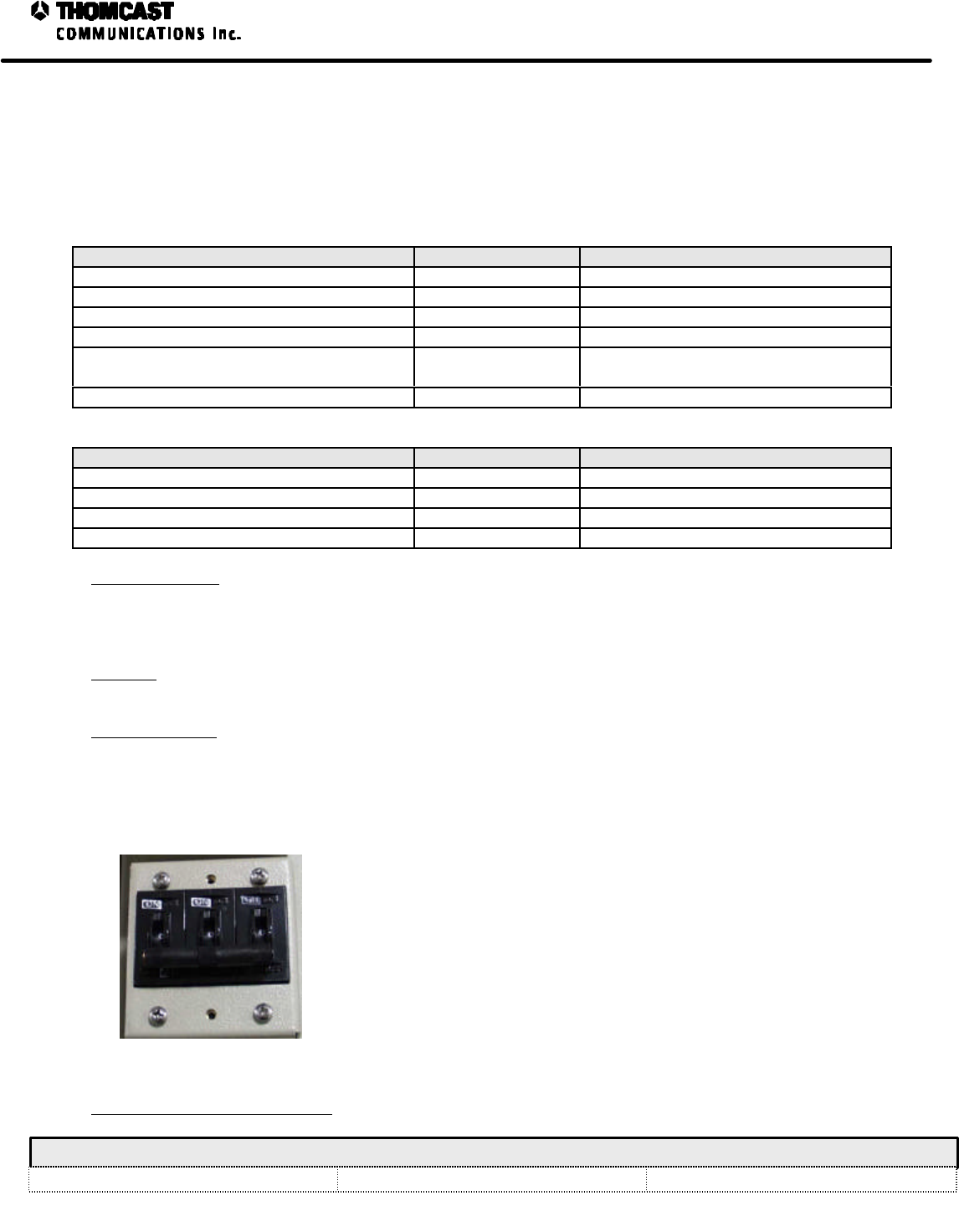
Figure 10: Circuit breaker.
A three-phase 15-Ampere circuit breaker is provided with each transmitter for
system protection. In a phase-to-phase system the circuit breaker is 25-
Ampere. It is located on the rear of the rack above the fans. When the current
exceeds its rating the circuit breaker trips and the transmitter, including AC to
DC front end converter, driver drawer, ultra low phase noise drawer (Agile
applications only), power amplifier segments and fans are shut down. A
plastic cover is provided to protect the circuit breaker from accidental shut
down.
16 Replace only with the same type and rating.
23
SD2500 TECHNICAL MANUAL
COMWAVE DIVISION
All information contained in this document is confidential and proprietary to THOMCAST and shall not be disclosed without the prior written permission of THOMCAST.
CREATED: KAS...................................................................12/9/99 CHECKED: DMW ................................................................12/9/99 RELEASED: PRC..................................................................12/9/99
Document #: DOC33-0040
REV: DEC.09.99
TROUBLESHOOTING WORKSHEET
DOC18-0011
This troubleshooting worksheet identifies each interface pin, the associated internal test point, nominal value, and the
expected voltage range. Please fill in all blank spaces completely.
J2: Rear Panel
Diagnostic Pin Function
Checked Low Limit
“VDC”Nominal
Voltage “VDC”High Limit
“VDC”Measured
Voltage
1Ground 0.00 0.00 0.00
2+12 V
DC PS +11.88 +12.00 +12.12
3-12 V
DC PS -12.12 -12.00 -11.88
4+11 V
DC PS +8.84 +11.00 +12.51
5+5 V
DC PS +4.50 +5.00 +5.50
6Mixer 0.98 1.95 2.86
7AMP 1 1.24 2.75 3.78
8AMP 2 0.88 1.08 1.46
9Final Q2 1.49 2.20 2.98
10 N/A N/A N/A N/A
11 N/A N/A N/A N/A
12 N/A N/A N/A N/A
13 System Reset 3.40 5.00 5.50
14 ALC 1.00 1.40 2.00
15 PA Standby 3.40 5.00 5.50
16 PA Fault 3.40 5.00 5.50
17 Driver Standby 3.40 5.00 5.50
18 Reset 1 3.40 5.00 5.50
19 Reset 2 3.40 +5.00 5.50
20 N/A N/A N/A N/A
21 LO 0.00 .30 1.02
22 Temp 0.00 0.70 2.50
23 FWD Power 0.74 1.40 2.32
24 N/A N/A N/A N/A
25 REFL Power 0.00 0.10 0.32
FILL IN ALL THE ABOVE BLANK SPACES COMPLETELY
COMPANY NAME: ________________________ CUSTOMER’S NAME: ________________________
PHONE NUMBER: ________________________ FAX NUMBER: ________________________
MODEL: __________ CHANNEL: ____________ SERIAL NUMBER (REAR PANEL): _____________
SEND RESULTS TO: THOMCAST COMMUNICATIONS, COMWAVE DIVISION
ATTENTION TECHNICAL SUPPORT
TOLL FREE PHONE (U.S.A. & Canada): 1-800-COMWAVE (1-800-266-9283)
International and U.S.A. 1-570-474-675115
FAX 1-570-474-5469
15 International calls must dial the country code before the phone number, i.e. 001-570-474-6751.
22
SD2500 TECHNICAL MANUAL
COMWAVE DIVISION
All information contained in this document is confidential and proprietary to THOMCAST and shall not be disclosed without the prior written permission of THOMCAST.
CREATED: KAS...................................................................12/9/99 CHECKED: DMW ................................................................12/9/99 RELEASED: PRC..................................................................12/9/99
Document #: DOC33-0040
REV: DEC.09.99
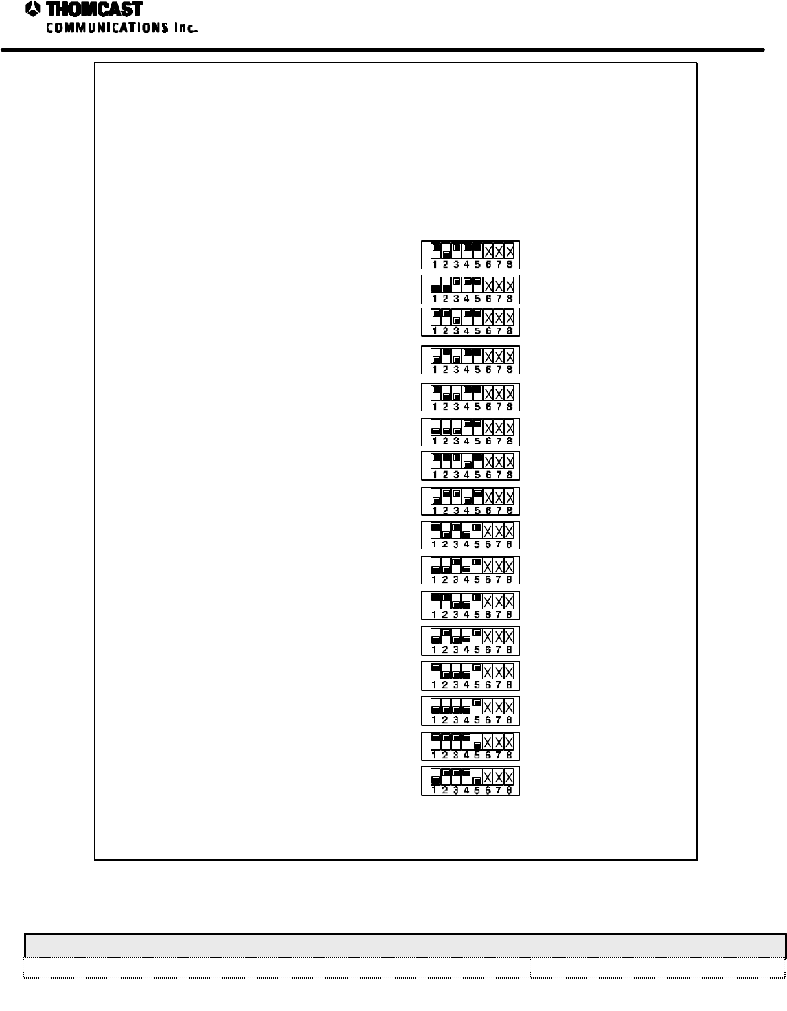
NODE ADDRESSES
1 to 16 Channels
NOTE: Do not change
node switch Settings 6, 7,
and 8. They should
remain as set by the
factory.
MODULE POSITION NODE ADDRESS NODE SWITCH SETTING
1ON
OFF
ON
OFF
ON
OFF
ON
OFF
ON
OFF
ON
OFF
ON
OFF
ON
OFF
ON
OFF
ON
OFF
ON
OFF
ON
OFF
ON
OFF
ON
OFF
ON
OFF
ON
OFF
2
2
3
4
4
3
6
5
5 6
7
8
9
7
8
910
14
15
16
17
12
13
1110
13
14
15
16
11
12
Figure 9: DOC22-0019 node addresses.

21
SD2500 TECHNICAL MANUAL
COMWAVE DIVISION
All information contained in this document is confidential and proprietary to THOMCAST and shall not be disclosed without the prior written permission of THOMCAST.
CREATED: KAS...................................................................12/9/99 CHECKED: DMW ................................................................12/9/99 RELEASED: PRC..................................................................12/9/99
Document #: DOC33-0040
REV: DEC.09.99
REFL PWR
(Reflected power is greater than 10%)
CAUSES: REMEDY:
Loose RF cable connection(s) Check integrity of all RF cable connections
RF cable kinked Check cabling for kinks or severe bends
Wave guide leak/depressurized Check wave guide pressure
Reflected metering out of adjustment Calibrate reflected metering per calibration
documentation in section 3 of the manual
Measure voltages at 25-pin diagnostic interface
FWD PWR
(Meter does not indicate 100% forward power)
CAUSES: REMEDY:
Driver Module Confirm output power
Final Module(s) Troubleshoot per front panel LED diagnostic display
Switching Power Supply Check for defective module
Forward metering out of adjustment Calibrate forward power metering per calibration
documentation in section 3 of the manual
Measure voltages at 25-pin diagnostic interface, J2
POWER AMPLIFIER SEGMENT
Hot replacement of the power amplifier segment may be required if a failure occurs. To remove a segment, turn the
key-lock switch to the OFF position, loosen the thumbscrews on the segment’s front panel and slide the failed
segment out of the sub-rack. Before the replacement segment can be installed, the node address must be set, refer to
document # DOC22-0019. A set of DIP switches is accessible through the cover of each segment directly behind
the key-lock switch. Set the DIP switches of the replacement segment to the same positions as the failed segment’s
DIP switches. Refer to the installation procedure in this manual to replace power amplifier segments.

20
SD2500 TECHNICAL MANUAL
COMWAVE DIVISION
All information contained in this document is confidential and proprietary to THOMCAST and shall not be disclosed without the prior written permission of THOMCAST.
CREATED: KAS...................................................................12/9/99 CHECKED: DMW ................................................................12/9/99 RELEASED: PRC..................................................................12/9/99
Document #: DOC33-0040
REV: DEC.09.99
-12 VDC
(Low or missing -12 VDC)
CAUSES: REMEDY:
Defective -12 V
DC source Check -12 V
DC source
Disconnected module Check module connectors
Shorted module Measure voltages at 25-pin diagnostic interface, J2
TEMPERATURE
(Internal chassis temperature exceeded +140 degrees Fahrenheit (+60 degrees Celsius)
CAUSES: REMEDY:
Fans inoperative Check fan operation
Heavy accumulation of debris on fans or heatsinks Check site air conditioning
Module(s) overheating Allow transmitter to cool, check latched failure logic by
rotating function switch momentarily to “STANDBY”
Site air conditioning Measure voltages at 25-pin diagnostic interface, J2
+11 VDC
(Switching power supply voltage has deviated beyond a set operating window {high or low}
CAUSES: REMEDY:
Defective main input line fuse Check switching power supply output voltage
Switching power supply module Check for defective fuses(s)
Open switching power supply fuse, F1 Measure voltages at 25-pin diagnostic interface, J2
Shorted amplifier module Measure voltages at 25-pin diagnostic interface, J2
Open motherboard fuse, F1
A 25-pin computer type diagnostic interface connector, labeled J2, is located on the rear of the chassis to assist in
troubleshooting. Critical power supply, module, and motherboard voltage test points can be accessed/monitored at
this location. Should a failure occur, the combination of meter readings, diagnostic LED status lights, and the
diagnostic interface voltage test points help identify the failure.
ANALOG METER
The analog meter provides a visual indication of the +11 V
DC switching power supply, peak relative forward or
reflected power. The +11 V
DC switching power supply and forward power should indicate 100%. Reflected power
meter readings less than 10% are typical.
+11 V PS
(Meter does not indicate 100%)
CAUSES: REMEDY:
Defective switching power supply Check for defective fuse(s)
Shorted module Check switching power supply output voltage
Open switching power supply fuse, F1 Troubleshoot per front panel LED diagnostic display
Switching power supply out of adjustment Adjust switching power supply output voltage per
calibration documentation is section 3 of the manual
Metering out of adjustment Calibrate meter per calibration documentation in
section 3 of the manual
Measure voltages at 25-pin diagnostic interface, J2
19
SD2500 TECHNICAL MANUAL
COMWAVE DIVISION
All information contained in this document is confidential and proprietary to THOMCAST and shall not be disclosed without the prior written permission of THOMCAST.
CREATED: KAS...................................................................12/9/99 CHECKED: DMW ................................................................12/9/99 RELEASED: PRC..................................................................12/9/99
Document #: DOC33-0040
REV: DEC.09.99
SD/SDA SERIES TROUBLESHOOTING
DOC18-0010
DRIVER
The driver is equipped with comprehensive diagnostic circuitry that monitors the status of power amplifier modules
and critical circuits so failures can be readily detected. Observing the front panel LED diagnostic display, analog
panel meter and diagnostic interface will inform you of the complete operational status. The following lists explain
various failure mode displays and possible solutions.
• NOTE: Due to internal transmitter design, there are no user serviceable modules, parts, or components. Repair of
these modules is not recommended or advised. Contact COMWAVE customer support should a failure occur.
The LED’s listed below continuously operate GREEN during normal operation. Absence of a green LED indicates
a missing signal or parameter that results in a controlled automatic shutdown
IN SIGNAL
(Missing IF input signal)
CAUSES: REMEDY:
Defective cabling to modulator baseband IF INPUT Check Cabling
Modulator Failure Verify IF source signal
Missing IF source signal Replace modulator
Measure voltages at 25-pin diagnostic interface, J2
INTERLOCK
(Missing system Interlock signal)
CAUSES: REMEDY:
RF module unplugged or shorted Check driver for disconnected module(s)
Measure voltages at 25-pin diagnostic interface, J2
The following LED’s continuously illuminate RED when a failure is detected. Controlled automatic transmitter shut
down is a function of the failure and severity. Presence of a RED status LED with normal meter readings and/or
normal transmitter operation indicates an out of tolerance condition with that circuit.
LO LEVEL
(Local Oscillator failure)
CAUSES: REMEDY:
Oscillator failure Check external cabling
10 MHz reference missing or low level Measure voltages at 25-pin diagnostic interface, J2
DRIVER
(Defective driver module)
CAUSES: REMEDY:
Driver module current Measure voltages at 25-pin diagnostic interface, J2
Power supply failure
FINAL
(Power Amplifier) (Defective final module.)
CAUSES: REMEDY:
Final module current Measure voltages at 25-pin diagnostic interface, J2
Power supply failure

18
SD2500 TECHNICAL MANUAL
COMWAVE DIVISION
All information contained in this document is confidential and proprietary to THOMCAST and shall not be disclosed without the prior written permission of THOMCAST.
CREATED: KAS...................................................................12/9/99 CHECKED: DMW ................................................................12/9/99 RELEASED: PRC..................................................................12/9/99
Document #: DOC33-0040
REV: DEC.09.99
TURN-ON PROCEDURE
DOC26-0003
• Before initial equipment turn-on, verify that all appropriate wiring interconnections have been accomplished
and the installation procedures have been followed precisely. Ensure proper AC power distribution to the
exhaust fans and cabling of the driver chassis and the ultra low phase noise drawer (Agile applications only).
INITIAL OPERATION PROCEDURE
Driver
1. Position the front panel rotary function switch to “STANDBY”.
2. Place the circuit breaker on the rear of the rack in the “ON” position.
3. The following GREEN LED’s continuously illuminate verifying successful initial operation:
ë IN SIGNAL (Modulator operation is required if an input signal is applied)
ë INTERLOCK (Motherboard IF presence switch, SW1, in by-pass, will cause false indication of IF
presence)
Power Amplifier Segment
No initial operation procedure is needed for the power amplifier segments. Proceed to the normal operation
procedures.
NORMAL OPERATION PROCEDURE
Driver
Rotating the function switch from “STANDBY” to any other position enables driver operation. Once the function
switch is rotated, the following GREEN LED’s continuously illuminate confirming normal operation:
ë IN SIGNAL
ë INTERLOCK
Absence of a green LED indicates a missing signal or parameter. Continuous illumination of any red status LED
indicates a failure has been detected by the diagnostic circuitry. Refer to troubleshooting guide.
To verify other transmitter parameters using the front panel meter, rotate the function switch. +11 V
DC PS and FWD
PWR should have meter readings of 100%. REFL PWR is a function of combiners, the transmission line, and
antenna. Reflected power readings less than 10% are typical.
Power Amplifier Segment
Power Amplifier Segment operation is accomplished by turning the key-lock switch to the “ON/LOCKED”
position.
• Note: The locks are an added safety feature; however, the keys are interchangeable.
The POWER/FAULT LED should continuously illuminate GREEN. If the LED flashes RED, the power amplifier
segment has faulted. After three faults, a failure will occur and the segment will shut down. Turning the key-lock
switch to the “OFF/UNLOCKED” position and then back to the “ON/LOCKED” position will reset it. Should
failure occur again, hot replacement is necessary. Turn the key-lock switch to the “OFF/UNLOCKED” position and
pull the failed segment out of the rack by the handle. Slide a new power amplifier segment into the vacant space, set
the correct node address, and turn the key-lock switch to the “ON/LOCKED” position. Refer to installation guide.
17
SD2500 TECHNICAL MANUAL
COMWAVE DIVISION
All information contained in this document is confidential and proprietary to THOMCAST and shall not be disclosed without the prior written permission of THOMCAST.
CREATED: KAS...................................................................12/9/99 CHECKED: DMW ................................................................12/9/99 RELEASED: PRC..................................................................12/9/99
Document #: DOC33-0040
REV: DEC.09.99
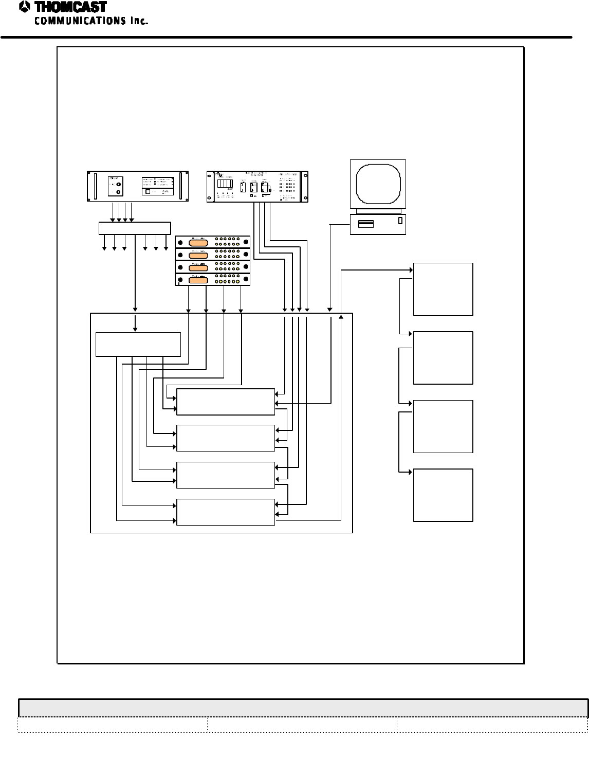
SD/SDA SERIES SYSTEM INTERCONNECTION
The following diagram is applicable to reference distribution, IF distribution, agile controller and ComView monitoring system installation
Transmitter 3
Transmitter 2
Transmitter 1
Transmitter 4
Splitter
Rack N
2
Rack N + 1
Rack N + 2
Rack N + 3
Rack N + 43
ModulatorsSplitter1
Comview
Monitoring
System
Agile ControllerReference Drawer
1. The type of splitter used is dependent upon the configuration of the transmitter.
2. A certain level must be obtained at this input, refer to the cabling document in section 2 of the manual.
3. The network end termination switch located on the rear panel of the driver must be set to TERM on the
last transmitter in the system (all other are set to OUT).
Figure 8: DOC30-0010 External interconnections.
COMWAVE DIVISION
All information contained in this document is confidential and proprietary to THOMCAST and shall not be disclosed without the prior written permission of THOMCAST.
CREATED: KAS 1/18/99 CHECKED: DMW 1/18/99 RELEASED: PRC 1/18/99
Document #: DOC30-0005 REV: NOV.11.99 ECO #: 98-116 1
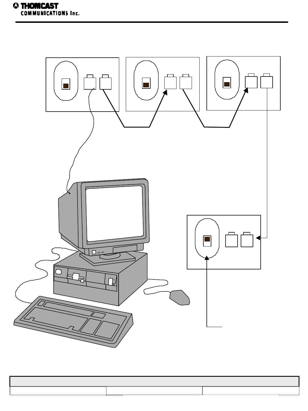
COMVIEW STATUS MONITORING INTERCONNECTIONS
COMWAVE
STATUS
MONITORING
SYSTEM
NOTE: Position
switch to TERM for last
drawer in the series
LAST DRAWER IN
SERIES
TO FINAL
DRAWER IN THE
SERIES
TERM
OUT
NETWORK END
TERMINATION NET NET
TERM
OUT
NETWORK END
TERMINATION NET NET
TERM
OUT
NETWORK END
TERMINATION NET NET
TERM
OUT
NETWORK END
TERMINATION NET NET
ComView Status Monitoring Interconnections
16
SD2500 TECHNICAL MANUAL
COMWAVE DIVISION
All information contained in this document is confidential and proprietary to THOMCAST and shall not be disclosed without the prior written permission of THOMCAST.
CREATED: KAS...................................................................12/9/99 CHECKED: DMW ................................................................12/9/99 RELEASED: PRC..................................................................12/9/99
Document #: DOC33-0040
REV: DEC.09.99
SD SERIES DRIVER CHASSIS CABLING
Figure 6: Driver chassis cabling.
TOP PANEL INTERFACE FOR THE SD/SDA/HPB SERIES OF
TRANSMITTERS/BOOSTERS
AC POWER
DISTRIBUTION
BOX
P6
P5
P4
P3
P2
P1
J5
J6
J7
J8
J9
FRONT OF RACK
P6 - Comview Input
P5 - Comview Output
P4 - Agile Control Input (Transmitter 4) (NOT USED IN THE HPB SYSTEM)
P3 - Agile Control Input (Transmitter 3) (NOT USED IN THE HPB SYSTEM)
P2 - Agile Control Input (Transmitter 2) (NOT USED IN THE HPB SYSTEM)
P1 - Agile Control Input (Transmitter 1) (NOT USED IN THE HPB SYSTEM)
J5 - Reference Signal Input
J6-J9 - IF Signal Input (Transmitters 1 through 4) (NOT USED IN THE HPB SYSTEM)
Figure 7: AC interface box.

15
SD2500 TECHNICAL MANUAL
COMWAVE DIVISION
All information contained in this document is confidential and proprietary to THOMCAST and shall not be disclosed without the prior written permission of THOMCAST.
CREATED: KAS...................................................................12/9/99 CHECKED: DMW ................................................................12/9/99 RELEASED: PRC..................................................................12/9/99
Document #: DOC33-0040
REV: DEC.09.99
CABLING FOR THE SD SERIES TRANSMITTER
DOC18-0019
DRIVER
Pull the driver out of the rack until the rack slides lock, to provide access to the rear panel of the driver chassis.
Wrap-around labels are located on each cable to denote proper destination. Refer to Figure6 for cabling details.
REFERENCE DISTRIBUTION
The reference drawer distributes a signal through the top of each rack, refer to the system interconnect diagram,
document # DOC30-0010, for more detail. The RG-59 coaxial cable enters the rack at connector J5. The level
should equal 15 +5 dB/-10 dB at the input of each rack (point 2 on the system interconnect diagram). This level
should be measured to determine if attenuation is needed. Place the appropriate size attenuator in-line with the
frequency reference input to the rack. Refer to Figure6 for cabling details.
IF DISTRIBUTION
The modulators that provide the IF signal are typically located in a separate rack. Cabling is accomplished by
distributing the modulator outputs using RG-59 coaxial cable to the top of each rack. Refer to the system
interconnect diagram, document # DOC30-0010 for more detail. The cables enter the top of the rack through
connectors J6 - J9 Refer to the top panel interface diagram, Figure7, for connector locations. The modulator levels
should be set to equal -15 dBm at the top of the rack.
COMVIEW INTERCONNECTIONS
ComView interconnections are achieved through six-conductor telephone cables with RJ-11 connectors at each end.
The first cabling harness exits the PC and enters the ComView Port P6 on the top of the rack, refer to the top panel
interface diagram, Figure7, for connector location. Once inside the rack, a second harness is cabled from a RJ-11
socket at the inside of the top of the rack to the net input on the RS-485 board of the first transmitter. Another
harness is cabled from the net output of the first transmitter to the net input of the second transmitter. This daisy
chain effect continues to the last transmitter in the rack. At the last transmitter in the rack, a harness is cabled from
the net out back to the top of the rack at connector, P5. This enables the cabling to continue in the same manner to
the next rack. Refer to the system interconnect diagram, document # DOC30-0010, for more detail on daisy chain
cabling. DOC30-0005 will also provide information regarding ComView interconnections.

14
SD2500 TECHNICAL MANUAL
COMWAVE DIVISION
All information contained in this document is confidential and proprietary to THOMCAST and shall not be disclosed without the prior written permission of THOMCAST.
CREATED: KAS...................................................................12/9/99 CHECKED: DMW ................................................................12/9/99 RELEASED: PRC..................................................................12/9/99
Document #: DOC33-0040
REV: DEC.09.99
Installation of the Driver Chassis
The rack is equipped with slide rails for convenient installation of the driver chassis. Slide rails also enable easy
access to internal adjustable controls and other maintenance/adjustments. To install the driver chassis in the rack,
pull the slide rails outward until they lock into place. Carefully align drawer with the slide rails and mate. Unlock
the slide rails by depressing the lock button on each rail while pushing the chassis inward. The chassis should slide
easily into rack. If binding occurs, rail-mounting brackets are in need of adjustment. Loosen brackets and
manipulate drawer to seat rails to match transmitter drawer. Tighten brackets once free sliding motion has been
achieved.
Once the driver chassis has been installed in the rack and the rack slides are adjusted, cabling can begin. Refer to
the cabling section of this manual for assistance.
Installation of the Power Amplifier Segments
The power amplifier segments slide into the sub-rack on nylon slides and connect to the motherboard via a floating
connector. The key-lock switch, located on the segment’s front panel, must be in the OFF position in order to plug
the segment into the sub-rack. This is to ensure that there is no arcing between connections before the segment is
fully engaged. Once the segment is slid into place, thumbscrews on the segment’s front panel are provided to fasten
the segment to the sub-rack and to provide additional ground connection. The key-lock switch may now be turned
to the ON position to apply power to the segment. Once the key-lock switch is turned on, the segment will
automatically set the gain and currents of the amplifier.
SYSTEM GROUNDING
For proper system operation, it is imperative that the system be adequately grounded. Each individual equipment
rack requires grounding to the main building ground. When bolting ground wires to racks, sand finish to remove
paint ensuring a good bond.
ENVIRONMENTAL AND SAFETY CONSIDERATIONS
Environmental Considerations
The equipment can be safely operated in ambient temperatures of -30 to +50 degrees Celsius (-22 to +122 degrees
Fahrenheit). However, moderate temperatures generally extend equipment life. Although the equipment may be
operated with relative humidity of up to 95%, the equipment must be protected from conditions that cause
condensation within the equipment.
A rear door is used to force proper ventilation through the cabinet (600 cfm fans per transmitter are used). If failure
of a fan occurs, replacement should be made as soon as possible. An air or temperature interlock should be
incorporated for protection against interruption of ventilation. The area should be kept dry and clean.
There should be sufficient space in front of the transmitter cabinet for the serviceman and test equipment plus the
full extension of the racked 27” deep chassis. A minimum of 36” behind the cabinet should be free for rear cabinet
access and air movement. Also, ample room must be available at the cabinet rear for cable placement.
Safety Considerations This equipment uses a grounding plug on all power cords. For personal safety, do not
defeat this safety feature. As with all similar types of equipment, high voltage can be
accessed when the driver chassis cover is removed. Special care should be given in
areas of fuses, line switches, and power supplies.
Modern high power solid state equipment contains low output voltage power supplies
with very high current capability. To prevent severe burns, avoid contact of rings;
watch bands, etc., with these circuits. When servicing the transmission line and
antenna, care must be taken to avoid exposure to high-energy microwave.
13
SD2500 TECHNICAL MANUAL
COMWAVE DIVISION
All information contained in this document is confidential and proprietary to THOMCAST and shall not be disclosed without the prior written permission of THOMCAST.
CREATED: KAS...................................................................12/9/99 CHECKED: DMW ................................................................12/9/99 RELEASED: PRC..................................................................12/9/99
Document #: DOC33-0040
REV: DEC.09.99
Non-Upgradeable Series
To begin mounting, align the holes on the bottom side of the notch filter to the slots located on the mounting
bracket. Insert the three #4-40 3/8” screws, flat washers and split-locking washers provided (do not tighten). Once
the notch filter is in place, connect it to the corresponding channel combiner and tighten the three #4-40 3/8” screws.
Now, the mounting bracket must be attached to the mounting plate. Align the bracket to the tapped holes in the
mounting plate and secure the bracket with the two #10-32 1/2” screws, flat washers and split-locking washers
provided. Finally, the mounting plate must be mounted to the top of the racks. Position the plate so that the holes in
the mounting plate correspond to the pre-drilled holes in the top of the racks. Secure the mounting plate to the top of
the racks using the three 1/4-20 3/4” bolts, nuts and split locking washers provided. See Figure5 for a pictorial.
• NOTE: The following diagram is not drawn to scale. The mounting plate is eight feet long, occupies
four rack-tops, and accommodates 16 notch filters.
Figure 5: Notch filter mounting for the upgradeable series of transmitters.

12
SD2500 TECHNICAL MANUAL
COMWAVE DIVISION
All information contained in this document is confidential and proprietary to THOMCAST and shall not be disclosed without the prior written permission of THOMCAST.
CREATED: KAS...................................................................12/9/99 CHECKED: DMW ................................................................12/9/99 RELEASED: PRC..................................................................12/9/99
Document #: DOC33-0040
REV: DEC.09.99
Notch Filter Mounting
The notch filters are mounted on the top of the rack(s). The upgradeable and non-upgradeable series have different
mounting plates and separate mounting instructions, refer to the instructions which correspond to your system.
Upgradeable Series
To begin mounting, align the holes on the bottom side of the notch filter to the slots located on the mounting
bracket. Insert the three #4-40 3/8” screws, flat washers, and split-locking washers provided (do not tighten
screws). Once the notch filter is in place, connect it to the corresponding channel combiner. Now, the mounting
bracket must be attached to the mounting plate, which is already installed on the top of the rack. Align the bracket
to the mounting plate slots, being sure the notch filter is in the desired location. Secure the mounting bracket with
two #10-32 1/2” screws, nuts, flat washers and split-locking washers provided. Finally, tighten the three, #4-40 3/8”
screws that secure the notch filter to the mounting bracket. Refer to Figure4 for a pictorial.
• This mounting system is designed to allow movement of the notch filter and mounting bracket. The
double-sided arrows denote motion. If a different position of the notch filter or mounting bracket is
desired, loosen the corresponding hardware, move to the new position, and retighten the hardware.
Figure 4: Notch filter mounting for the upgradeable series of transmitters.

11
SD2500 TECHNICAL MANUAL
COMWAVE DIVISION
All information contained in this document is confidential and proprietary to THOMCAST and shall not be disclosed without the prior written permission of THOMCAST.
CREATED: KAS...................................................................12/9/99 CHECKED: DMW ................................................................12/9/99 RELEASED: PRC..................................................................12/9/99
Document #: DOC33-0040
REV: DEC.09.99
Channel Combiner Mounting
See Figure3 for numerical references. A 99-093-02-option kit is typically used to mount the channel combiners to
the top of the rack. To begin mounting, the C-Channel must be fastened to the top of the rack. Refer to Bubble #1
for a magnified view of mounting the C-Channel to the rack. Align the pre-drilled holes of the C-Channel (A) to the
pre-existing #10-32 2” screws, nuts, and split-locking washers (B) in the top of the rack. Insert hole A onto
hardware B and secure with a nut and split-locking washer as shown.
Once the C-Channels are mounted to the top of the rack, the channel combiners can be attached to the C-Channels.
Refer to Bubble #2 for mounting the channel combiner to the C-Channel. Align the holes on the feet of the channel
combiner (A) to the pre-drilled holes in the C-Channel (B). Secure the channel combiner foot A with the 1/4-20
1/2” bolt and split-locking washer provided. If pre-existing holes cannot be found on the C-Channel, stage the
channel combiners on the floor and determine where the combiner’s feet will rest on the mounting channel. Drill
holes in the mounting channel to accommodate the channel combiner feet. Secure the feet with the 1/4-20 1/2”
bolts, split-locking washers and nuts provided. After the channel combiners are mounted in place, the notch filter
can be mounted to the top of the rack. Proceed to the next section for detailed instructions.
Figure 3: Channel combiner mounting.

10
SD2500 TECHNICAL MANUAL
COMWAVE DIVISION
All information contained in this document is confidential and proprietary to THOMCAST and shall not be disclosed without the prior written permission of THOMCAST.
CREATED: KAS...................................................................12/9/99 CHECKED: DMW ................................................................12/9/99 RELEASED: PRC..................................................................12/9/99
Document #: DOC33-0040
REV: DEC.09.99
Bolting the Racks Together
A minimum of six bolts should be used to bolt each rack to the adjacent (three in the front and three in the rear).
After all of the racks have been placed in their final destination; insert the provided hardware in the accessible-side-
panel holes of the racks. The hardware can be located on the bottom side of the racks. Refer to Figure2 for hole
locations.
• NOTE: Be sure that all three exposed planes of the Racks are straight and flush before the bolts are
tightened.
After the racks are bolted together, bolt the side-panels to the ends of the outer racks.
Side-Panel
Holes
Figure 2: Racks.

9
SD2500 TECHNICAL MANUAL
COMWAVE DIVISION
All information contained in this document is confidential and proprietary to THOMCAST and shall not be disclosed without the prior written permission of THOMCAST.
CREATED: KAS...................................................................12/9/99 CHECKED: DMW ................................................................12/9/99 RELEASED: PRC..................................................................12/9/99
Document #: DOC33-0040
REV: DEC.09.99
INSTALLATION PROCEDURE
DOC17-0006
UNPACKING
The racks should remain in their original packing containers until they are placed in the equipment shelter. Place all
racks outside of the shelter sequentially so they can be installed in their proper position. Packing materials should
be removed from the racks inside the equipment shelter as they are being installed.
The drivers and power amplifier segments should be removed from their boxes, as they are ready to be installed.
Any unused equipment should remain in the original packing box until needed. As each piece of equipment is being
unpacked, compare the packing list with the contents of the box and check for in-transit damage. Should any
damage be noted, notify the freight carrier immediately to file a freight claim. Also, notify Comwave of any
damages or of materials missing from the shipment. Refer to the customer service document # DOC20-0001 for
information about contacting Comwave.
Please do not discard original packaging material. It should be returned to Comwave to be
recycled. Be sure to retain several boxes for each type of equipment at the transmitting site.
This is to be used in the event the equipment is shipped back to the factory for repairs,
upgrades, or modifications to ensure adequate protection.
PHYSICAL INSTALLATION:
Installation of the Rear Door
Install the rear door of each transmitter as it is unpacked. Place the hinged portion of the door over the
corresponding holes in the fan shroud assembly. Insert the screws provided into the existing rack clips. After
adjusting the door position, close and lock the door to ensure proper mechanical operation.
AC Power Connections to the Exhaust Fans
The exhaust fans located on the rear door of the rack have attached wiring harnesses. The harnesses must be routed
into the transmitter chassis through a hole in the fan shroud and connected to the AC terminal strip. The terminal
strip must be accessed before the racks are bolted together. Verify that the circuit breaker is in the OFF position.
Connect the fan harness to the terminal strip.
8
SD2500 TECHNICAL MANUAL
COMWAVE DIVISION
All information contained in this document is confidential and proprietary to THOMCAST and shall not be disclosed without the prior written permission of THOMCAST.
CREATED: KAS...................................................................12/9/99 CHECKED: DMW ................................................................12/9/99 RELEASED: PRC..................................................................12/9/99
Document #: DOC33-0040
REV: DEC.09.99
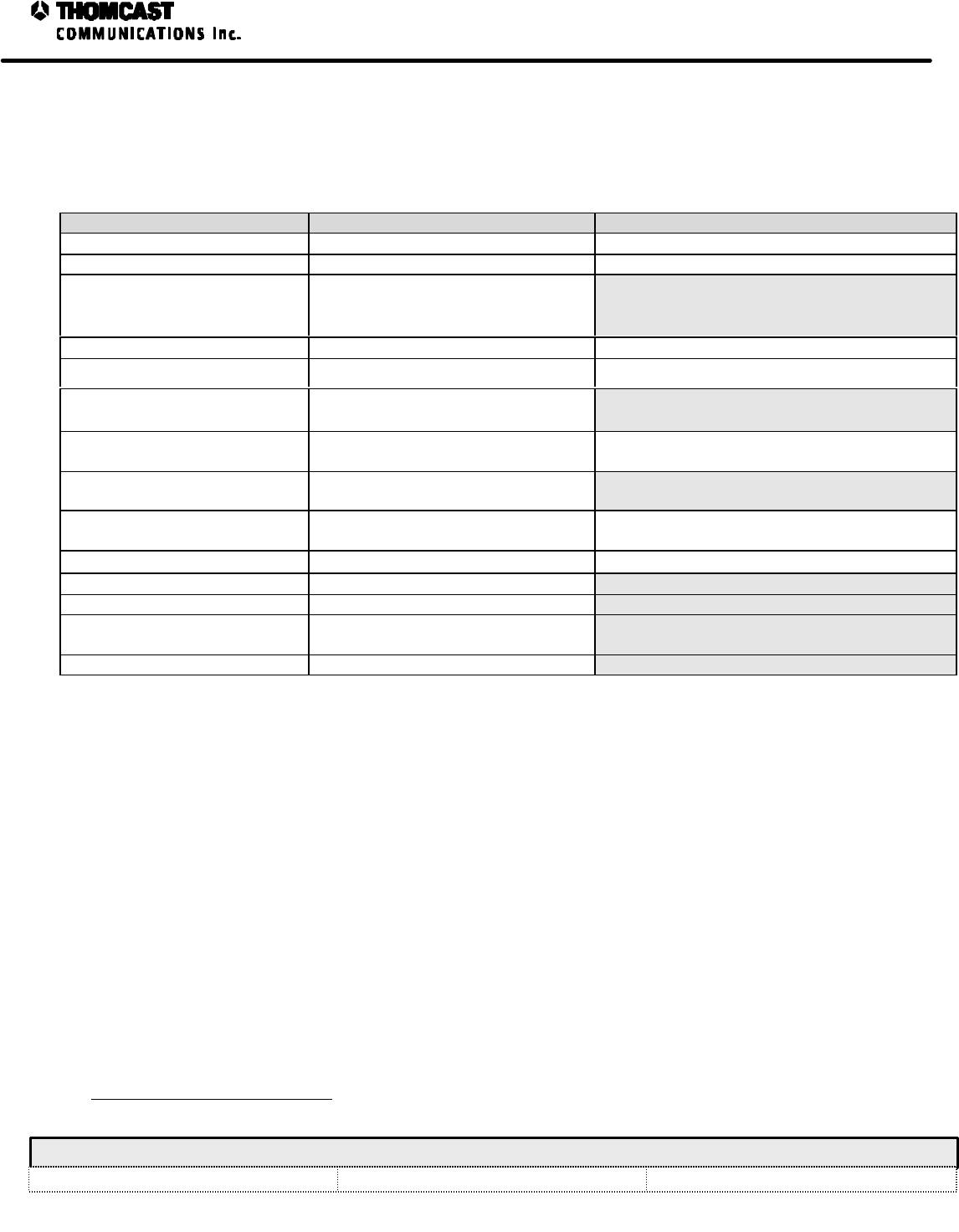
Parameter Specification Notes / Test Conditions
AURAL PERFORMANCE
Output Power12 15 dB visual/aural ratio
+0.5 dB to -2 dB
Measured at transmitter output
Other ratios available upon request
IF Input Level
Impedance/Connector -23 dBm peak ± 2 dB
75O / female BNC Combined visual and aural
Emission 250KF3E or per CCIR
Inter Carrier Frequency Accuracy = ± 50 Hz relative to visual carrier
Frequency Response
13, 14
Mono
Stereo = ± 1 dB 30 Hz to 15 KHz
= ± 1 dB 50 Hz to 105 KHz w/o pre-
emphasis
Pre-emphasis 50 or 75 microseconds (defeatable)
Deviation ±25 KHz (System M/N) (±50 KHz Stereo)
±50 KHz (System B/G/D/K/I) NICAM
and IRT Stereo compatible
Harmonic Distortion13, 14 = 1%
FM Noise13, 14 = -60 dB
Audio Input Level13
Mono @ ±25 KHz deviation
Mono @ ±50 KHz deviation
Stereo @ ±50 KHz deviation
-10 to +10 dBm into 600Ω
-10 to +10 dBm into 600Ω
-10 to +10 dBm
GENERAL
Power Requirement (Line PF =0.95)
Operating
Stand-by Mode
117/230 V
AC ±10%; 50/60 Hz
<900 VA
<950 VA
Operating Temperature 0°C to +50°CFrequency stability and equipment functionality
guaranteed
Specified Temperature Range 13° to +33°CAll Specified parameters guaranteed
Relative Humidity 95% non-condensing
Vertical Rack Requirement 12.25” Does not include modulator
Dimensions 15.75” H x 21.1” W x 34.5” D
40.0cm H x 53.6 cm W x 87.6 cm D
Approximate Shipping Weight 215 lb (97.40 kg)
12 In band intermodulation specification is based on 15 dB visual to aural ratio. Contact factory for specification change due to other ratios
13 Using TVM-102 modulator
14 Factory video/audio performance test limits may include up to 50% of the test demodulator measurement uncertainty.
7
SD2500 TECHNICAL MANUAL
COMWAVE DIVISION
All information contained in this document is confidential and proprietary to THOMCAST and shall not be disclosed without the prior written permission of THOMCAST.
CREATED: KAS...................................................................12/9/99 CHECKED: DMW ................................................................12/9/99 RELEASED: PRC..................................................................12/9/99
Document #: DOC33-0040
REV: DEC.09.99
Parameter Specification Notes / Test Conditions
ANALOG
VISUAL PERFORMANCE
Output Power 10 - 100 Watts Peak Sync Adjustable from 10 to 100% of peak sync power
Output Frequency Any 6, 7, or 8 MHz Channel 2000 - 2700 MHz
In select bands
Emission 5M75C3F or per CCIR
Impedance/Connector
Input
Output 75Ω/F female
50Ω/N female
Input Level Video 1 VP-P ± 6dB
IF Input Level
Impedance/Connector
-8 dBm peak ± 2 dB
75O / female BNC
Frequency Stability = ± 500 Hz
= ± 1 Hz (Optional GPS)
Frequency Response
8, 9, 10 = ± 1 dB FCC Multiburst video pattern
Group Delay 8, 10 Per FCC 73.687(a)(3) or per CCIR Sin(x)/x video pattern
Harmonics = -60 dBc Measured in 30 KHz RBW at transmitter output
relative to visual carrier (unmodulated carriers)
Spurious Products 8= -60 dBc (out of band) Measured in 30 KHz RBW at transmitter output
relative to visual carrier using 75% color bars
video pattern
Intermodulation Distortion (IM3)11 = -60 dBc (in band) Measured in 100 KHz RBW at transmitter output
relative to visual carrier using red field video
pattern
Differential Gain8, 10 = 3% NTC-7 composite video pattern
Differential Phase8, 10 = 2°NTC-7 composite video pattern
Sync Pulse Amplitude8, 10 = ±5% NTC-7 composite video pattern
Luminance Non-linearity8, 10 = 3% NTC-7 composite video pattern
Weighted SNR8, 10 = 55 dB Quiet Line - Line 12
Hum and Noise8, 10 = 60 dB
K Factor 2T8, 10 = 2% NTC-7 composite video pattern
Incidental Carrier Phase8, 10
Modulation (I.C.P.M.) = 3°NTC-7 composite video pattern
RF Output Regulation = ± 0.2 dB
SSB Phase Noise
Direct measurement of microwave LO = -80 dBc/Hz @ 10 KHz offset
= -110 dBc/Hz @ 10 KHz offset
Standard
Optional (recommended for digital transmission)
8 Using TVM-102 modulator.
9 Spectral occupancy per FCC ruling for both analog and digital
10 Factory video/audio performance test limits may include up to 50% of the test demodulator measurement uncertainty.
11 In band intermodulation specification is based on 15 dB visual to aural ratio. Contact factory for specification change due to other ratios

6
SD2500 TECHNICAL MANUAL
COMWAVE DIVISION
All information contained in this document is confidential and proprietary to THOMCAST and shall not be disclosed without the prior written permission of THOMCAST.
CREATED: KAS...................................................................12/9/99 CHECKED: DMW ................................................................12/9/99 RELEASED: PRC..................................................................12/9/99
Document #: DOC33-0040
REV: DEC.09.99
SD2500 TRANSMITTER SPECIFICATIONS TRANSMITTER1
DOC19-0087
Parameter Specification Notes / Test Conditions
DIGITAL
Average Output Power 2 - 25 Watts 223-1 PN data sequence (at transmitter output)
IF Input Frequency 44 MHz Other frequency options available
Impedance/Connector
Input
Output 75 Ω/BNC-female
50 Ω/N-female
Average Input Power -15 dBm ± 0.5 dB 223-1 PN data sequence (at transmitter output)
Output Frequency 2000 - 2700 MHz In select bands
Frequency Response
2≤ ±0.25 dB FC ±2.6 MHz
Measured at channel combiner output
Frequency Stability ≤ ±500 Hz
≤ ±1 Hz (Optional GPS)
Carrier to Noise (C/N) ≥ 55 dB
Hum and Noise ≤ -60 dBc
Group Delay2≤ ±15 ns FC ±2.6 MHz
Measured at channel combiner output
Digital Modulation
Error Vector Magnitude 2, 3 (EVM) ≤ 2.0% 64-QAM/8-VSB @ 5.06 Msps RMS average over
12,500 symbols
Measured at channel combiner output
Digital Modulation
Signal to Noise Ratio 2,3 (SNR) ≥ 30 dB 64-QAM/8-VSB @ 5.06 Msps RMS average over
12,500 symbols
Measured at channel combiner output
Magnitude Linearity
(AM-AM conversion) ≤ ±0.125 dB Measured at channel combiner output
Phase Linearity
(AM-PM conversion) ≤ ±0.75°Measured at channel combiner output
Adjacent Channel Interference4, 5
(FCC ATV Spectral Mask) Sidelobe power spectral density (PSD)
≤ -38 dB at channel edge; decreasing to
≤ -60dB at ±3 MHz from channel edge
Relative to in-band average PSD measured @ 100
KHz RBW at the channel combiner output
Harmonics 6≤ -60 dBc Relative to unmodulated carrier power measured
@ 100 KHz RBW at the channel combiner output
Spurious Products7≤ -60 dBc Relative to unmodulated carrier power measured
@ 100 KHz RBW at the channel combiner output
RF Output Regulation ≤ ± .2 dB Measured at transmitter output
SSB Phase Noise
Direct measurement of microwave LO = -80 dBc/Hz @ 10 KHz offset
= -110 dBc/Hz @ 10 KHz offset Optional
Standard (recommended for digital transmission)
1 All factory test measurements made at approximately 23°C.
2 Upconverter amplifier drawer with optional group delay and frequency equalizer @ the output of the non-adjacent channel combiner.
3 Or equivalent threshold BER measurement.
4 Spectral occupancy per FCC ruling for both analog and digital
5 Measured with a non-adjacent channel combiner, notch filter and optional IF equalizer module.
6 Undesired signal power 2 dB higher than the nominal PSD of the adjacent spectral regions that is harmonically related to unmodulated carrier
7 Undesired signal power 2 dB higher than the nominal PSD of the adjacent spectral regions that is harmonically related to internal system
signals such as clock, LOs, etc.

5
SD2500 TECHNICAL MANUAL
COMWAVE DIVISION
All information contained in this document is confidential and proprietary to THOMCAST and shall not be disclosed without the prior written permission of THOMCAST.
CREATED: KAS...................................................................12/9/99 CHECKED: DMW ................................................................12/9/99 RELEASED: PRC..................................................................12/9/99
Document #: DOC33-0040
REV: DEC.09.99
• NOTE: ALL SPECIFICATIONS
CONTAINED WITHIN THIS
MANUAL ARE SUBJECT TO
CHANGE WITHOUT NOTICE.

4
SD2500 TECHNICAL MANUAL
COMWAVE DIVISION
All information contained in this document is confidential and proprietary to THOMCAST and shall not be disclosed without the prior written permission of THOMCAST.
CREATED: KAS...................................................................12/9/99 CHECKED: DMW ................................................................12/9/99 RELEASED: PRC..................................................................12/9/99
Document #: DOC33-0040
REV: DEC.09.99
MONTHLY MAINTENANCE RECORD --------------------------------------------------------------------------------------------27
DOC18-0006------------------------------------------------------------------------------------------------------------------------------27
DIGITAL DRIVER THEORY OF OPERATION---------------------------------------------------------------------------------28
DOC14-0035------------------------------------------------------------------------------------------------------------------------------28
FRONT PANEL-------------------------------------------------------------------------------------------------------------------------------28
REAR PANEL---------------------------------------------------------------------------------------------------------------------------------29
SD-SERIES FREQUENCY FIXED DIGITAL DRIVER (2RU) SPECIFICATIONS ---------------------------------32
DOC19-0008------------------------------------------------------------------------------------------------------------------------------32
POWER AMPLIFIER SEGMENT THEORY OF OPERATION------------------------------------------------------------33
DOC14-0008------------------------------------------------------------------------------------------------------------------------------33
OPERATION -------------------------------------------------------------------------------------------------------------------------------------33
POWER AMPLIFIER SEGMENT SPECIFICATIONS ------------------------------------------------------------------------34
CUSTOMER SERVICE---------------------------------------------------------------------------------------------------------------------35
DOC20-0001------------------------------------------------------------------------------------------------------------------------------35
CONTACT INFORMATION -------------------------------------------------------------------------------------------------------------35
COMMENTS/SUGGESTIONS-----------------------------------------------------------------------------------------------------------35
EQUIPMENT RETURNS ------------------------------------------------------------------------------------------------------------------35
RETURN PACKAGING ----------------------------------------------------------------------------------------------------------------------36
RETURN PACKAGING OF THE POWER AMPLIFER SEGMENT-----------------------------------------------------37
TABLE OF FIGURES
Figure 1: SD2500 transmitting system..........................................................................................................................................1
Figure 2: Racks...............................................................................................................................................................................10
Figure 3: Channel combiner mounting.......................................................................................................................................11
Figure 4: Notch filter mounting for the upgradeable series of transmitters.........................................................................12
Figure 5: Notch filter mounting for the upgradeable series of transmitters.........................................................................13
Figure 6: Driver chassis cabling..................................................................................................................................................16
Figure 7: AC interface box............................................................................................................................................................16
Figure 8: DOC30-0010 External interconnections...................................................................................................................17
Figure 9: DOC22-0019 node addresses......................................................................................................................................22
Figure 10: Circuit breaker. ............................................................................................................................................................24
Figure 11: Internal view of driver................................................................................................................................................25
Figure 12: Power amplifier segment heatsink. ..........................................................................................................................26
Figure 13: Blanking panel & exhaust fans.................................................................................................................................26
Figure 14: Driver front and rear panels......................................................................................................................................30
Figure 15: Driver layout................................................................................................................................................................31
Figure 16: Power amplifier segment...........................................................................................................................................33
Figure 17 : DOC15-0013 power amplifier segment block diagram. .....................................................................................33
Figure 18: Equipment packing.....................................................................................................................................................36
Figure 19: Empty power amplifier segment box. ......................................................................................................................37
Figure 20: Boxed power amplifier segment...............................................................................................................................37
Figure 21: Power amplifier segments ready to ship.................................................................................................................38
TABLE OF TABLES
Table 1: Driver fuse locations......................................................................................................................................................24
Table 2: Power amplifier segment fuse locations.....................................................................................................................24
Table 3: DOC19-0014, REV D....................................................................................................................................................34

3
SD2500 TECHNICAL MANUAL
COMWAVE DIVISION
All information contained in this document is confidential and proprietary to THOMCAST and shall not be disclosed without the prior written permission of THOMCAST.
CREATED: KAS...................................................................12/9/99 CHECKED: DMW ................................................................12/9/99 RELEASED: PRC..................................................................12/9/99
Document #: DOC33-0040
REV: DEC.09.99
TABLE OF CONTENTS
THOMCAST COMMUNICATIONS, COMWAVE DIVISION TWO YEAR LIMITED WARRANTY---------2
DOC12-0001------------------------------------------------------------------------------------------------------------------------------- 2
SD2500 TRANSMITTER SPECIFICATIONS TRANSMITTER --------------------------------------------------------------6
DOC19-0087------------------------------------------------------------------------------------------------------------------------------- 6
INSTALLATION PROCEDURE----------------------------------------------------------------------------------------------------------9
DOC17-0006------------------------------------------------------------------------------------------------------------------------------- 9
UNPACKING-------------------------------------------------------------------------------------------------------------------------------------- 9
PHYSICAL INSTALLATION:------------------------------------------------------------------------------------------------------------------- 9
Installation of the Rear Door------------------------------------------------------------------------------------------------------------9
Upgradeable Series---------------------------------------------------------------------------------------------------------------------- 12
SYSTEM GROUNDING-------------------------------------------------------------------------------------------------------------------------14
ENVIRONMENTAL AND SAFETY CONSIDERATIONS------------------------------------------------------------------------------------14
CABLING FOR THE SD SERIES TRANSMITTER-----------------------------------------------------------------------------15
DOC18-0019------------------------------------------------------------------------------------------------------------------------------15
DRIVER-----------------------------------------------------------------------------------------------------------------------------------------15
REFERENCE DISTRIBUTION -----------------------------------------------------------------------------------------------------------------15
IF DISTRIBUTION------------------------------------------------------------------------------------------------------------------------------15
COMVIEW INTERCONNECTIONS------------------------------------------------------------------------------------------------------------15
TURN-ON PROCEDURE------------------------------------------------------------------------------------------------------------------18
DOC26-0003------------------------------------------------------------------------------------------------------------------------------18
INITIAL OPERATION PROCEDURE----------------------------------------------------------------------------------------------------------18
Driver---------------------------------------------------------------------------------------------------------------------------------------- 18
Power Amplifier Segment -------------------------------------------------------------------------------------------------------------- 18
NORMAL OPERATION PROCEDURE--------------------------------------------------------------------------------------------------------18
Driver---------------------------------------------------------------------------------------------------------------------------------------- 18
Power Amplifier Segment -------------------------------------------------------------------------------------------------------------- 18
SD/SDA SERIES TROUBLESHOOTING--------------------------------------------------------------------------------------------19
DOC18-0010------------------------------------------------------------------------------------------------------------------------------19
DRIVER-----------------------------------------------------------------------------------------------------------------------------------------19
ANALOG METER ------------------------------------------------------------------------------------------------------------------------ 20
POWER AMPLIFIER SEGMENT-------------------------------------------------------------------------------------------------------21
TROUBLESHOOTING WORKSHEET ----------------------------------------------------------------------------------------------23
DOC18-0011------------------------------------------------------------------------------------------------------------------------------23
EQUIPMENT FUSING AND PROTECTION --------------------------------------------------------------------------------------24
DOC18-0009------------------------------------------------------------------------------------------------------------------------------24
MAINTENANCE------------------------------------------------------------------------------------------------------------------------------25
DOC18-0012------------------------------------------------------------------------------------------------------------------------------25
INSPECTIONS------------------------------------------------------------------------------------------------------------------------------------25
CLEANING------------------------------------------------------------------------------------------------------------------------------------25
DRIVER: ------------------------------------------------------------------------------------------------------------------------------------ 25
POWER AMPLIFIER SEGMENTS:-------------------------------------------------------------------------------------------------26
POWER SUPPLY:------------------------------------------------------------------------------------------------------------------------ 26
EXHAUST FANS:------------------------------------------------------------------------------------------------------------------------- 26

2
SD2500 TECHNICAL MANUAL
COMWAVE DIVISION
All information contained in this document is confidential and proprietary to THOMCAST and shall not be disclosed without the prior written permission of THOMCAST.
CREATED: KAS...................................................................12/9/99 CHECKED: DMW ................................................................12/9/99 RELEASED: PRC..................................................................12/9/99
Document #: DOC33-0040
REV: DEC.09.99
THOMCAST COMMUNICATIONS, COMWAVE DIVISION TWO YEAR
LIMITED WARRANTY
DOC12-0001
Thomcast warrants each product of its manufacture to be free from any defect in material and workmanship for a
period of two years after delivery to, and return by the original purchaser. No returns, however, will be accepted
unless accompanied by a written factory return authorization.
The limit of liability under this warranty shall be to repair or replace any product, or part thereof, which proves to be
defective after inspection by Thomcast with the exception of tubes, semiconductor devices, lamps, fuses or
equipment (i.e. modulators) manufactured by others, which are subject to only such loss adjustment as Thomcast
may obtain for the suppliers thereof.
This warranty shall not apply to any Thomcast product which has been modified, physically or electrically damaged,
or to modules which seals have been broken, or any product which has been subjected to conditions exceeding the
applicable specifications or ratings or improper service techniques.
Thomcast will not be liable for any direct or consequential injury, loss or damage incurred through the use, or the
inability to use, any Thomcast product.
Thomcast reserves the right to make design changes to any Thomcast product without incurring any obligation to
make the same changes to previously purchased units.
This warranty is the full extent of the obligation and liability assumed by Thomcast with respect to any and all
Thomcast products. Thomcast neither makes, nor authorizes any person to make, any other guarantee or warranty
concerning Thomcast products.

1
SD2500 TECHNICAL MANUAL
COMWAVE DIVISION
All information contained in this document is confidential and proprietary to THOMCAST and shall not be disclosed without the prior written permission of THOMCAST.
CREATED: KAS...................................................................12/9/99 CHECKED: DMW ................................................................12/9/99 RELEASED: PRC..................................................................12/9/99
Document #: DOC33-0040
REV: DEC.09.99
Figure 1: SD2500 transmitting system.
TECHNICAL MANUAL
DOC33-0040
SD2500 - 25 Watt Digital Transmitter System
COMWAVE DIVISION