Toshiba 6F3B0253 Users Manual
2014-12-13
: Toshiba Toshiba-6F3B0253-Users-Manual-131794 toshiba-6f3b0253-users-manual-131794 toshiba pdf
Open the PDF directly: View PDF ![]() .
.
Page Count: 301 [warning: Documents this large are best viewed by clicking the View PDF Link!]

6F3B0253
UM-TS01∗∗∗-E031
PROGRAMMABLE CONTROLLER
PROSEC T1- 16S
USER’S MANUAL
−
−−
− Basic Hardware and Function −
−−
−
TOSHIBA CORPORATION
6F3B0253
Important Information
Misuse of this equipment can result in property damage or human injury.
Because controlled system applications vary widely, you should satisfy yourself
as to the acceptability of this equipment for your intended purpose.
In no event will Toshiba Corporation be responsible or liable for either indirect
or consequential damage or injury that may result from the use of this equipment.
No patent liability is assumed by Toshiba Corporation with respect to use of
information, illustrations, circuits, equipment or examples of application in this
publication.
Toshiba Corporation reserves the right to make changes and improvements to this
publication and/or related products at any time without notice. No obligation shall be
incurred other than as noted in this publication.
This publication is copyrighted and contains proprietary material. No part of this book
may be reproduced, stored in a retrieval system, or transmitted, in any form or by any
means electrical, mechanical, photocopying, recording, or otherwise without
obtaining prior written permission from Toshiba Corporation.
© TOSHIBA Corporation 2001. All rights reserved
IBM is a registered trademark of International Business Machines Corporation.
MS-DOS and Windows are registered trademarks of Microsoft Corporation.
Publication number: UM-TS01∗∗∗-E031
1st edition April 2001, 2nd edition November 2001

6F3B0253
Basic Hardware and Function 1
CE Marking
The Programmable Controller PROSEC T1-16S (hereafter called T1-16S) complies with the
requirements of the EMC Directive 89/336/EEC and Low Voltage Directive 72/23/EEC under the
condition of use according to the instructions described in this manual.
The contents of the conformity are shown below.
Application of EMC : 89/336/EEC (as amended by 91/263/EEC and 92/31/EEC)
Council Directive LVD : 72/23/EEC (as amended by 93/68/EEC)
Manufacture’s Name : Toshiba Corporation,
Fuchu Operations-Social Infrastructure Systems
Address : 1, Toshiba-Cho
Fuchu-shi
TOKYO 183-8511
Japan
declares, that the product
Product Name : Programmable Controller , T1-16S
Model Number : TDR116S6S, TDR116S6C
TDR116S3S, TDR116S3C
conforms to the following Product Specifications:
EMC
Radiated Interference : EN 55011 Group 1 Class A
Mains Interference : EN 55011 Group 1 Class A
Radiated Susceptibility : ENV50140
Conducted RFI Susceptibility : ENV50141, IEC100-4-6.
Electrostatic Discharge : IEC1000-4-2
Electrical Fast Transient : IEC1000-4-4
LVD : EN61131-2:1995 3.10 Dielectric Properties
4. Mechanical Requirements
Supplementary information :
(1) Included Handy Programmer THP911A*S.
(2) Included each type of associated input/output unit in a typical configuration.
(3) Product must be installed in accordance with manufacturers instructions

6F3B0253
2 T1-16S User’s Manual
UL/c-UL Listing
The Programmable Controller PROSEC T1-16S (hereafter called T1-16S) is UL/c-UL listed as
shown below.
UL and c-UL Listing
File Number : E95637
Product Name : Programmable Controller , T1-16S
Product Covered : Main Unit
TDR116S6S, TDR116S6C,
TDR116S3S, TDR116S3C
I/O module
TDI116M*S, TDD116M*S, TDO116M*S,
TAD121M*S, TAD131M*S, TDA121M*S, TDA131M*S,
TFR112M*S
Peripherals
TRM102**S, TCU111**S, THP911A*S
UL and c-UL Listing For Use in Hazardous Locations
File Number : E184034
Product Name : Programmable Controller , T1-16S
Product Covered : Main Unit
TDR116S6S, TDR116S6C
Locations Class : Class I, Division 2, Groups A, B, C, D
Important Notice : 1. THIS EQUIPMENT IS SUITABLE FOR USE IN CLASS I,
DIVISION 2, GROUPS A, B, C, D OR NON-HAZARDOUS
LOCATIONS ONLY.
2. WARNING - EXPLOSION HAZARD - SUBSTITUTION OF
COMPONENTS MAY IMPAIR SUITABILITY FOR CLASS I,
DIVISION 2.
3. WARNING - EXPLOSION HAZARD - DO NOT DISCONNECT
EQUIPMENT UNLESS POWER HAS BEEN SWITCHED OFF
OR THE AREA IS KNOWN TO BE NON-HAZARDOUS.

6F3B0253
Basic Hardware and Function 3
Safety Precautions
This manual is prepared for users of Toshiba’s Programmable Controller T1-16S.
Read this manual thoroughly before using the T1-16S. Also, keep this manual and related
manuals so that you can read them anytime while the T1-16S is in operation.
General Information
1. The T1-16S has been designed and manufactured for use in an industrial
environment. However, the T1-16S is not intended to be used for systems which may
endanger human life. Consult Toshiba if you intend to use the T1-16S for a special
application, such as transportation machines, medical apparatus, aviation and space
systems, nuclear controls, submarine systems, etc.
2. The T1-16S has been manufactured under strict quality control. However, to keep
safety of overall automated system, fail-safe systems should be considered outside
the T1-16S.
3. In installation, wiring, operation and maintenance of the T1-16S, it is assumed that the
users have general knowledge of industrial electric control systems.
If this product is handled or operated improperly, electrical shock, fire or damage to
this product could result.
4. This manual has been written for users who are familiar with Programmable
Controllers and industrial control equipment. Contact Toshiba if you have any
questions about this manual.
5. Sample programs and circuits described in this manual are provided for explaining the
operations and applications of the T1-16S. You should test completely if you use them
as a part of your application system.
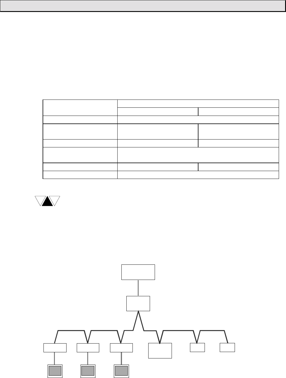
Hazard Classifications
In this manual, the following two hazard classifications are used to explain the safety
precautions.
Indicates a potentially hazardous situation which, if not avoided, could
result in death or serious injury.
Indicates a potentially hazardous situation which, if not avoided, may
result in minor or moderate injury. It may also be used to alert
against unsafe practices.
Even a precaution is classified as CAUTION, it may cause serious results depending on
the situation. Observe all the safety precautions described on this manual.
!WARNING
!CAUTION

6F3B0253
4 T1-16S User’s Manual
Safety Precautions
Installation:
1. Excess temperature, humidity, vibration, shocks, or dusty and corrosive gas
environment can cause electrical shock, fire or malfunction. Install and use the T1-
16S and related equipment in the environment described in this manual.
2. Improper installation directions or insufficient installation can cause fire or the units
to drop. Install the T1-16S and related equipment in accordance with the instructions
described in this manual.
3. Turn off power before installing or removing any units, modules, racks, terminal
blocks or battery. Failure to do so can cause electrical shock or damage to the T1-
16S and related equipment.
4. Entering wire scraps or other foreign debris into to the T1-16S and related
equipment can cause fire or malfunction. Pay attention to prevent entering them into
the T1-16S and related equipment during installation and wiring.
5. Turn off power immediately if the T1-16S or related equipment is emitting smoke or
odor. Operation under such situation can cause fire or electrical shock. Also
unauthorized repairing will cause fire or serious accidents. Do not attempt to repair.
Contact Toshiba for repairing.
Wiring:
1. Turn off power before wiring to minimize the risk of electrical shock.
2. Exposed conductive parts of wire can cause electrical shock. Use crimp-style
terminals with insulating sheath or insulating tape to cover the conductive parts. Also
close the terminal covers securely on the terminal blocks when wiring has been
completed.
3. Operation without grounding may cause electrical shock or malfunction. Connect the
ground terminal on the T1-16S to the system ground.
4. Applying excess power voltage to the T1-16S can cause explosion or fire. Apply
power of the specified ratings described in the manual.
5. Improper wiring can cause fire, electrical shock or malfunction. Observe local
regulations on wiring and grounding.
!CAUTION
!CAUTION

6F3B0253
Basic Hardware and Function 5
Safety Precautions
Operation:
1. Configure emergency stop and safety interlocking circuits outside the T1-16S.
Otherwise, malfunction of the T1-16S can cause injury or serious accidents.
2. Operate the T1-16S and the related modules with closing the terminal covers. Keep
hands away from terminals while power on, to avoid the risk of electrical shock.
3. When you attempt to perform force outputs, RUN/HALT controls, etc. during
operation, carefully check for safety.
4. Turn on power to the T1-16S before turning on power to the loads. Failure to do so
may cause unexpected behavior of the loads.
5. Do not use any modules of the T1-16S for the purpose other than specified. This
can cause electrical shock or injury.
6. Do not modify the T1-16S and related equipment in hardware nor software. This can
cause fire, electrical shock or injury.
7. Configure the external circuit so that the external 24 Vdc power required for
transistor output circuits and power to the loads are switched on/off simultaneously.
Also, turn off power to the loads before turning off power to the T1-16S.
8. Install fuses appropriate to the load current in the external circuits for the outputs.
Failure to do so can cause fire in case of load over-current.
9. Check for proper connections on wires, connectors and modules. Insufficient contact
can cause malfunction or damage to the T1-16S and related equipment.
!WARNING
!CAUTION

6F3B0253
6 T1-16S User’s Manual
Safety Precautions
Maintenance:
1. Turn off power before removing or replacing units, modules, terminal blocks or wires.
Failure to do so can cause electrical shock or damage to the T1-16S and related
equipment.
2. When you remove both input and output terminal blocks with wires for maintenance
purpose, pay attention to prevent inserting them upside down.
3. Touch a grounded metal part to discharge the static electricity on your body before
touching the equipment.
4. Otherwise, charged static electricity on your body can cause malfunction or failure.
5. Do not disassemble the T1-16S because there are hazardous voltage parts inside.
6. Perform daily checks, periodical checks and cleaning to maintain the system in
normal condition and to prevent unnecessary troubles.
7. Check by referring “Troubleshooting” section of this manual when operating
improperly. Contact Toshiba for repairing if the T1-16S or related equipment is failed.
Toshiba will not guarantee proper operation nor safety for unauthorized repairing.
8. The contact reliability of the output relays will reduce if the switching exceeds the
specified life. Replace the unit or module if exceeded.
9. The battery used in T1-16S may present a risk of fire of chemical burn if mistreated.
Do not recharge, disassemble, heat above 100ºC (212ºF), or incinerate.
10. Replace battery with CR2032 only. Use of another battery may present a risk of fire
or explosion.
11. Dispose of used battery promptly. Keep away from children. Do not disassemble
and do not dispose of in fire.
!CAUTION
6F3B0253
Basic Hardware and Function 7
Safety Precautions
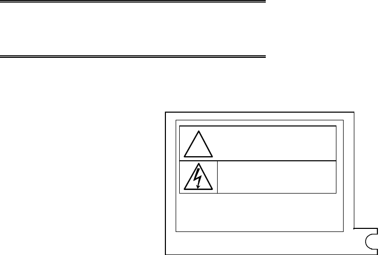
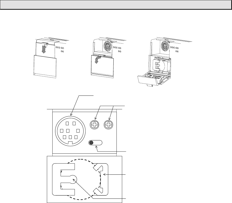
Safety Label
The safety label as shown on the right is
attached to the power terminal of the
T1-16S.
Remove the mount paper before wiring.
Peel off the label from the mount paper
and stick it near the power terminals
where it can be readily seen.
Contact Toshiba if the label is damaged.
!
Do not touch terminals
while power on.
CAUTION
Hazardous voltage can shock, burn or cause death.
Do not touch terminals while power on.
Read related manual thoroughly for safety.
Stick this seal on unit or near unit.
Take off this sheet before wiring.

6F3B0253
8 T1-16S User’s Manual
About This Manual
About This Manual
This manual has been prepared for first-time users of Toshiba’s Programmable Controller
T1-16S to enable a full understanding of the configuration of the equipment, and to
enable the user to obtain the maximum benefits of the equipment.
This manual introduces the T1-16S, and explains the system configuration,
specifications, installation and wiring for T1-16S’s basic hardware. This manual provides
the information for designing T1-16S user program, such as the internal operation,
memory configuration, I/O allocation and programming instructions. Information for
maintenance and troubleshooting are also provided in this manual.
The T1-16S’s computer link function and T1-16S’s multi-purpose communication
functions are covered by the separate manual. Read the T1-16S User’s Manual -
Communication Function - for details.
Inside This Manual
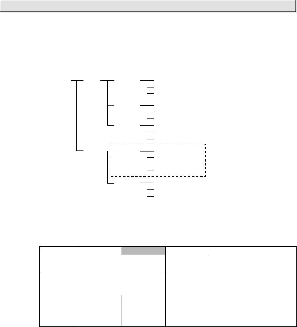
This manual consists of 10 main sections and an appendix.
Section 1 outlines the T1-16S configuration. To fully understand the T1-16S, it is
important to read this section carefully. Sections 2, to 4 describe the hardware used in
designing external circuits and panels. Sections 5 to 7 are mainly concerned with
software. Section 8 explains the T1-16S’s special I/O functions. Sections 9 and 10
describe the maintenance procedure for the T1-16S, to ensure safe operation and long
service life.
Related Manuals
The following related manuals are available for T1-16S. Besides this manual, read the
following manuals for your better understanding.
T1-16S User’s Manual
- Basic Hardware and Function - (this manual) UM-TS01∗∗∗-E031
- I/O Modules - UM-TS01∗∗∗-E034
- Communication Function - UM-TS01∗∗∗-E033
T-Series Handy Programmer (HP911) Operation Manual UM-TS03∗∗∗-E025
T-Series Program Development System (T-PDS) User’s Manual UM-TS03∗∗∗-E045

6F3B0253
Basic Hardware and Function 9
About This Manual
Terminology
The following is a list of abbreviations and acronyms used in this manual.
µ
µµ
µsmicrosecond
ASCII American Standard Code For Information Interchange
AWG American Wire Gage
BCC Block Check Code
CCW Counter-Clockwise
CPU Central Processing Unit
CW Clockwise
EEPROM Electrically Erasable Programmable Read Only Memory
Hhexadecimal (when it appears in front of an alphanumeric string)
I/O Input/Output
LED Light Emitting Diode
LSB Least Significant Bit
ms millisecond
MSB Most Significant Bit
PWM Pulse Width Modulation
RAM Random Access Memory
ROM Read Only Memory
Vac AC voltage
Vdc DC voltage

6F3B0253
10 T1-16S User’s Manual
Contents
Contents
Safety Precautions .................................................................................. 3
About This Manual .................................................................................. 8
1. System Configuration .................................................................... 13
1.1 Introducing the T1-16S ................................................................ 14
1.2 Features .............................................................................................. 16
1.3 System configuration .......................................................................... 19
1.4 I/O expansion ...................................................................................... 20
1.5 Components ........................................................................................ 21
1.5.1 Basic unit ......................................................................................... 21
1.5.2 I/O modules ...................................................................................... 25
1.5.3 Options ............................................................................................ 26
1.6 Programmer port function .................................................................. 27
1.7 RS-485 port communication function ................................................. 28
1.8 Real-time data link system ................................................................. 32
1.9 Peripheral tools .................................................................................. 33
2. Specifications .................................................................................. 37
2.1 General specifications ........................................................................ 38
2.2 Functional specifications .................................................................... 40
2.3 I/O specifications ................................................................................ 42
2.4 External dimensions ........................................................................... 46
3. I/O Application Precautions .......................................................... 47
3.1 Application precautions for input signals ............................................ 48
3.2 Application precautions for output signals .......................................... 50
4. Installation and Wiring ................................................................... 53
4.1 Environmental conditions ................................................................... 54
4.2 Installing the unit ................................................................................. 55
4.3 Wiring terminals .................................................................................. 57
4.4 Grounding ........................................................................................... 58
4.5 Power supply wiring ............................................................................ 59
4.6 I/O wiring ............................................................................................ 61

6F3B0253
Basic Hardware and Function 11
Contents
5. Operating System Overview ......................................................... 63
5.1 Operation modes ................................................................................ 64
5.2 About the built-in EEPROM ................................................................ 66
5.3 Scanning ............................................................................................. 69
6. Programming Information ............................................................. 73
6.1 Devices and registers ......................................................................... 74
6.2 Index modification ............................................................................... 86
6.3 Real-time clock/calendar .................................................................... 88
6.4 I/O allocation ....................................................................................... 89
6.5 T1-16S memory mode setting.............................................................. 91
6.6 User program configuration ................................................................ 92
6.6.1 Main program .................................................................................. 94
6.6.2 Sub-program #1 .............................................................................. 95
6.6.3 Timer interrupt program .................................................................. 95
6.6.4 I/O interrupt programs ..................................................................... 96
6.6.5 Subroutines .................................................................................... 97
6.7 Programming language ...................................................................... 98
6.8 Program execution sequence ............................................................ 99
6.9 On-line debug support functions ........................................................ 100
6.10 Password protection ........................................................................... 103
7. Instructions ...................................................................................... 105
7.1 List of instructions .............................................................................. 106
7.2 Instruction specifications .................................................................... 116
8. Special I/O Functions .................................................................... 255
8.1 Special I/O function overview ............................................................. 256
8.2 Variable input filter constant .............................................................. 260
8.3 High speed counter ............................................................................ 261
8.3.1 Single phase up-counter ................................................................. 262
8.3.2 Single phase speed-counter ............................................................ 263
8.3.3 Quadrature bi-pulse counter ............................................................ 265
8.4 Interrupt input function ........................................................................ 268
8.5 Analog setting function ....................................................................... 270
8.6 Pulse output function .......................................................................... 271
8.7 PWM output function .......................................................................... 273
9. Maintenance and Checks .............................................................. 275
9.1 Precautions during operation ............................................................. 276
9.2 Daily checks ........................................................................................ 277
9.3 Periodic checks ................................................................................... 278
9.4 Maintenance parts ............................................................................... 279
9.5 Battery ................................................................................................. 280

6F3B0253
12 T1-16S User’s Manual
Contents
10. Troubleshooting .............................................................................. 281
10.1 Troubleshooting procedure ................................................................ 282
10.1.1 Power supply check ......................................................................... 283
10.1.2 CPU check ....................................................................................... 284
10.1.3 Program check ................................................................................. 284
10.1.4 Input check ....................................................................................... 285
10.1.5 Output check .................................................................................... 286
10.1.6 Environmental problem .................................................................... 287
10.2 Self-diagnostic items .......................................................................... 288
Appendix ......................................................................................................... 293
A.1 List of models and types ..................................................................... 294
A.2 Instruction index ................................................................................. 295

6F3B0253
Basic Hardware and Function 13
Section 1
System Configuration
1.1 Introducing the T1-16S, 14
1.2 Features, 16
1.3 System configuration, 19
1.4 I/O expansion, 20
1.5 Components, 21
1.6 Computer link system, 27
1.7 T1-16S Communication function, 28
1.8 Real-time data link system, 32
1.9 Peripheral tools, 33
6F3B0253
14 T1-16S User’s Manual
1. System Configuration
1.1 Introducing the T1-16S
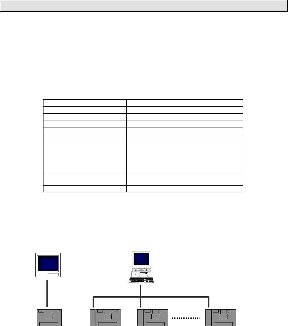
The T1-16 is compact, block style, high-performance programmable controller with a
range of 16 to 144 input and output points.
The figure below shows the T1 Series line-up. The T1 Series consists of the total 16
types.
T1 Series T1 T1-16 T1-MDR16
T1-MAR16
T1-MDR16D
T1-28 T1-MDR28
T1-MAR28
T1-MDR28D
T1-40 T1-MDR40
T1-MAR40
T1-MDR40D
T1S T1-16S T1-MDR16SS
T1-MDR16SC
T1-MDR16SSD
T1-MDR16SCD
T1-40S T1-MDR40S
T1-MAR40S
T1-MDR40SD
I/O points:
The T1 Series are available in five models, T1-16, T1-28, T1-40, T1-40S and T1-
16S. Each model has the following I/O points.
T1-16 T1-16S T1-28 T1-40 T1-40S
Input 8 points 14 points 24 points
Output 8 points
(6 relay plus 2 slid-state) 14 points
(12 relay plus
2 slid-state)
16 points
(14 relay plus 2 solid-state)
Expansion No Up to 8 I/O
modules.
Total up to
144 points.
No 2 option cards plus
1 expansion rack or unit.
Total up to 382 points.
The T1-16S can expand its I/O points by connecting I/O modules. Up to eight I/O
modules can be connected. If eight 16-point I/O modules are connected to the T1-
16S, it can control up to 144 points.

6F3B0253
Basic Hardware and Function 15
1. System Configuration
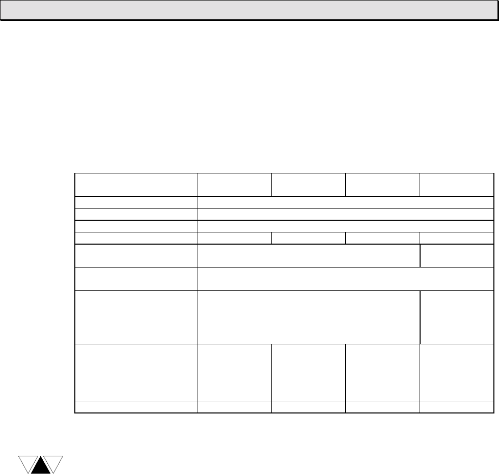
Memory capacity:
Program memory capacity of the T1 is 2 k steps. And that of the T1S is 8 k steps.
Whole the program and a part of data registers are stored in built-in EEPROM.
T1-16/28/40 T1-40S T1-16S
Memory RAM (for execution) and EEPROM (for back-up)
Program
capacity 2 k steps 8 k steps
(4 k mode or 8 k mode)
Data capacity Auxiliary relay: 1024 points
Timer: 64 points
Counter: 64 points
Data register: 1024 words
Auxiliary relay: 4096 points
Timer: 256 points
Counter: 256 points
Data register: 4096 words
EEPROM
back-up Program and leading 512
words of Data register Program and the user specified range of
Data register (0 to 2048 words)
Capacitor: 1 hour
or more
RAM back-up
(at 25°C)
(at 77°F)
Capacitor: 6 hours or more Capacitor: 168 hours
or more
Battery: 2 years
or more
Control functions:
In addition to the basic relay ladder functions, the T1/T1S provides functions such as
data operations, arithmetic operations, various functions, etc. Furthermore, its high-
speed counter functions, pulse output functions and data communication functions
allow its application to a wide scope of control systems.
T1-16/28/40 T1-40S T1-16S
Language Ladder diagram with function block
Number of
instructions Basic: 17 types
Function: 76 types Basic: 21 types
Function: 99 types Basic: 21 types
Function: 97 types
Subroutines 16
(nesting not allowed) 256
(up to 3 levels of nesting)
Execution speed 1.4 µs/contact, 2.3 µs/coil, 4.2 µs/transfer, 6.5 µs/addition
Real-time
clock/calendar No Yes (year, month, day, week, hours,
minutes, seconds)
Communication RS-232C
(programmer port) RS-232C (programmer port),
RS-485 (multi-purpose)
Construction:
The T1-16S is a compact, easy-handling block style programmable controller. The
T1-16S has all of the features of a block style controller. In addition, the T1-16S has
modular expandability. The T1-16S provides flexibility into the block style controller.
Series compatibility:
Programming instructions are upward compatible in the T-Series programmable
controllers. The T1/T1S programs can be used for other models of the T-Series, T2,
T2E, T2N, T3 and T3H. Peripheral tools can also be shared.

6F3B0253
16 T1-16S User’s Manual
1. System Configuration
1.2 Features
I/O module support:
The T1-16S has an interface for connecting the I/O modules. Up to eight modules
can be connected to the T1-16S.
By using the 16 points I/O module, the T1-16S can control up to 144 I/O points.
Built-in high-speed counter:
Two single-phase or one quadrature (2-phase) pulses can be counted. The
acceptable pulse rate is up to 5 kHz. (DC input type only)
Built-in analog setting adjusters:
Two analog setting adjusters are provided on the T1-16S. This allows operators to
adjust time or other control parameters easily using a screwdriver.
High speed processing:
Sophisticated machine control applications require high speed data manipulations.
The T1-16S is designed to meet these requirements.
• 1.4 µs per contact • 2.3 µs per coil
• 4.2 µs per 16-bit transfer • 6.5 µs per 16-bit addition
The T1-16S also supports interrupt input function (DC input type only). This allows
immediate operation independent of program scan.
High performance software:
The T1-16S offers 21 basic ladder instructions and 97 function instructions.
Subroutines, Interrupt functions, Indirect addressing, For/Next loops, Pre-derivative
real PID, etc. are standard on the T1-16S. These functions allow the T1-16S to be
applied to the most demanding control applications.
Battery-less operation:
The T1-16S has a standard built-in EEPROM, permitting operation without need of a
battery. Also, the variable data can be written into and/or read from the EEPROM,
providing completely maintenance-free back-up operation.
This function is an important feature for OEMs, because it can eliminate the need for
changing the battery every few years.
(Optional battery is also available to back-up real-time clock and retentive data)

6F3B0253
Basic Hardware and Function 17
1. System Configuration
Pulse output / PWM output:
One point of variable frequency pulses (max. 5 kHz) or variable duty pulses can be
output. These functions can be used to drive a stepping motor or to simulate an
analog output. (DC input type only)
Built-in computer link function:
The T1-16S’s RS-232C programmer port can accept the computer link protocol (data
read/write). This results in easy connection to a higher level computer, an operator
interface unit, etc.
The parity setting of the programmer port can be selected either odd or none. The
none parity mode is provided especially for telephone modem connection. Using
modems, remote programming/monitoring is available.
Real-time control data link network:
By connecting the TOSLINE-F10 remote module (FR112M) to the T1 -16S, high-
speed data link network can be established. In this network, upper T-series PLC
model (T2/T2E/T2N or T3/T3H) works as master and up to 16 T1-16Ss can be
connected as remote. Each T1-16S can exchange data with the master through 1
word input and 1 word output. The transmission speed can be selected either 750
kbps or 250 kbps.
Sampling trace function:
The sampling trace is the function to collect the user specified data every user
specified timing (minimum every scan), and to display the collected data on the
programmer screen in time chart and/or trend graph format. This function is useful
for checking the input signals changing.
Password protection:
By registering your passwords, four levels of protection is available according to the
security levels required for your application.
Level 4: Reading/writing program and writing data are prohibited
Level 3: Reading/writing program are prohibited
Level 2: Writing program is prohibited
Level 1: No protection (changing passwords is available only in this level)
Two points of solid-state output:
Each model of the T1-16S has two points of solid-state output (transistors for DC
input type and triacs for AC input type). These solid-state outputs are suitable for
frequent switching application.

6F3B0253
18 T1-16S User’s Manual
1. System Configuration
DIN rail mounting:
The T1-16S is equipped with brackets for mounting on a standard 35 mm DIN rail.
The T1-16S can be mounted on a DIN rail as well as screw mounting.
On-line program changes:
When the T1-16S’s memory mode is set to 4 k steps mode, on-line (in RUN mode)
program changes are available. Furthermore, program writing into the built-in
EEPROM is also available in RUN mode. These functions are useful in program
debugging stage.
Real-time clock/calendar function: (Enhanced model only)
The T1-16S has the real-time-clock/calendar function (year, month, day, day of the
week, hours, minutes, seconds) that can be used for performing scheduled
operations, data gathering with time stamps, etc. To back-up the real-time
clock/calendar data, use of the optional battery is recommended.
RS-485 multi-purpose communication port: (Enhanced model only)
The T1-16S has an RS-485 multi-purpose communication port. Using this port, one
of the following communication modes can be selected.
•
••
•Computer link mode: T-series computer link protocol can be used in this mode.
Up to 32 T1-16Ss can be connected to a master computer. By using this mode,
MMI/SCADA system can be easily configured.
•
••
•Data link mode: Two PLCs (any combination of T1S, T2E or T2N) can be
directly linked together. This direct link is inexpensive, easily configured and
requires no special programming.
•
••
•Free ASCII mode: User defined ASCII messages can be transmitted and
received through this port. A terminal, printer, bar-code reader, or other serial
ASCII device can be directly connected.
•
••
•Inverter connection mode: This mode is specially provided to communicate with
Toshiba Inverters (ASDs) VF-A7/G7/S9 series. By using this function, the T1-16S
can control and monitor the connected Inverters.
6F3B0253
Basic Hardware and Function 19
1. System Configuration
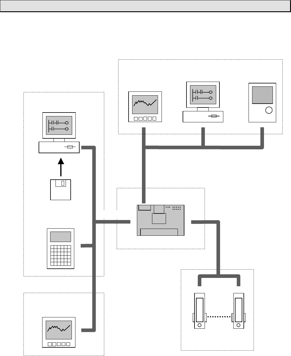
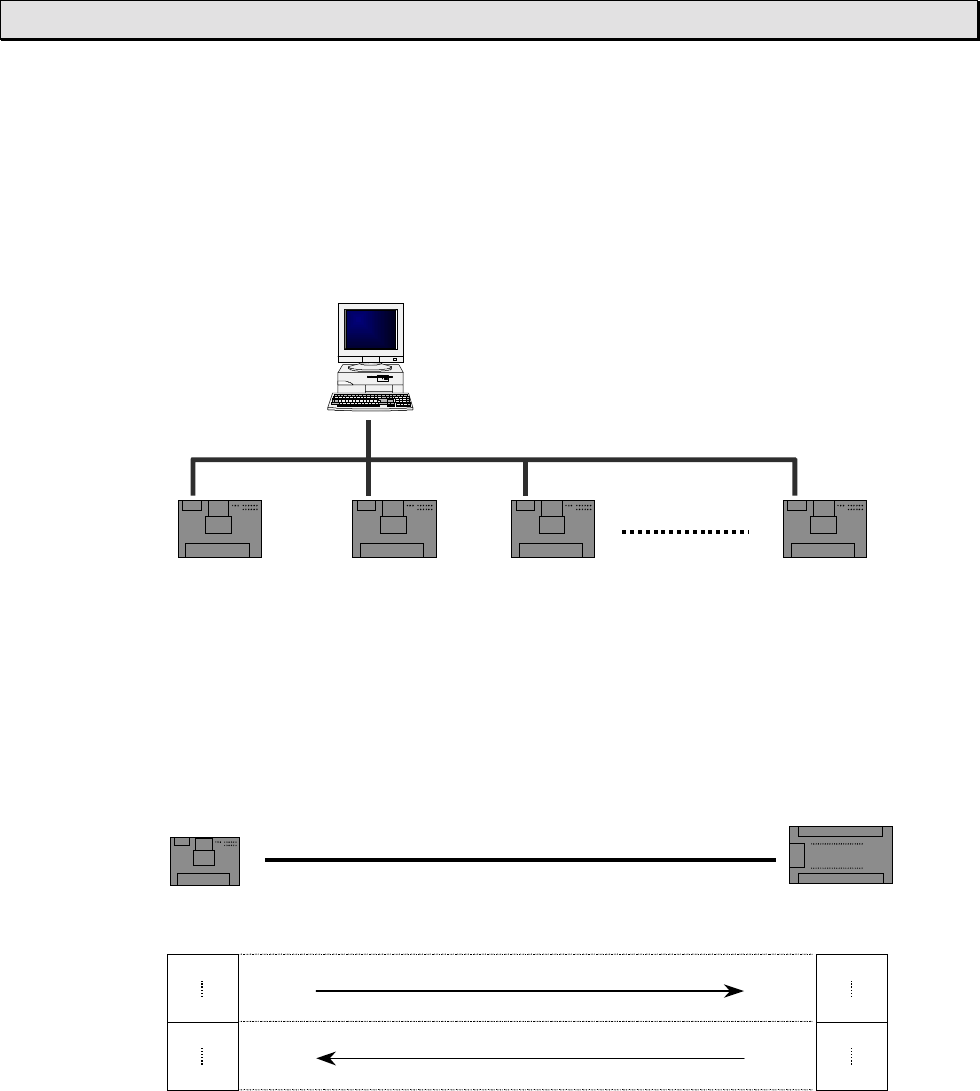
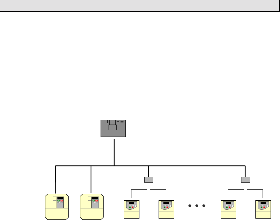
1.3 System configuration
The following figure shows the T1-16S system configuration.
IBM-PC compatible
personal computer
T-PDS
software
Handy programmer
HP911A
T1-16S basic unit
Peripheral tool
I/O modules
Computer link function
MMI/SCADA
system
8 modules max.
T1-16S
RS232C
IBM-PC compatible
personal computer
RS485 (Standard type only)
MMI/SCADA
system Inverter
6F3B0253
20 T1-16S User’s Manual
1. System Configuration
1.4 I/O expansion
The T1-16S provides I/O expandability by connecting the I/O modules. Up to eight
I/O modules can be connected.
Available I/O modules
DI116M: 16 points DC input
DO116M: 16 points DC output
DD116M: 8 points DC input + 8 points DC output
RO108M: 8 points relay output
AD121M: 1 channel analog input (0 to 5V or 0 to 20mA)
AD131M: 1 channel analog input (-10 to +10V)
DA121M: 1 channel analog output (0 to 20mA)
DA131M: 1 channel analog output (-10 to +10V)
TC111M: 1 channel thermocouple input (type K, J, E, or ±50mV)
FR112M: TOSLINE-F10 remote station
T1-16S maximum configuration
(1) The 5Vdc power to the I/O modules is supplied from the main unit. The main
unit can supply maximum 1.5A of the 5Vdc power to the I/O modules. Check
the current consumption of each I/O module used. Refer to section 2.1.
(2) The connecting order of the I/O modules is not restricted except TOSLINE-
F10 remote station FR112M. When the FR112M is used, it must be the right
end module.
(3) If more than 8 I/O modules are connected, the T1-16S cannot operate
normally.
T1-16S
main unit
Up to 8 I/O modules
NOTE

6F3B0253
Basic Hardware and Function 21
1. System Configuration
1.5 Components
1.5.1 Basic unit
The T1-16S is available in four types as shown in the following table.
Type
Link/ Calendar
Power supply
Input
Output
T1-MDR16SS
(Enhanced model)
Yes
T1-MDR16SC
(Standard model)
No
100-240 Vac,
50/60 Hz
T1-MDR16SSD
(Enhanced model)
Yes
T1-MDR16SCD
(Standard model)
No
24 Vdc
8 points - 24 Vdc
6 points - relay,
2 points - transistor
Power supply and
input/output terminals
Link terminals
(Enhanced model only)
Programmer
port cover
Battery holder
cover
Operation status LEDs
I/O status LEDs (Low side)
I/O status LEDs (High side)
Mounting hole
Expantion
connector
6F3B0253
22 T1-16S User’s Manual
1. System Configuration
♦ Behind the programmer port cover
PRG
H/R
V1 V0
Programmer port connector
Analog setting adjusters
(V0 and V1)
Mode control switch
(HALT / RUN)
Battery holder
Battery type: CR2032
(Optional)
A tab for battery eject
Power supply terminals:
Connect the power cable and grounding wire. The terminal screw size is M3.
See sections 4.4 and 4.5 for wiring.
Input terminals:
Connect input signal wires. The terminal screw size is M3. See section 2.4 for
details.
Output terminals:
Connect output signal wires. The terminal screw size is M3. See section 2.4 for
details.
6F3B0253
Basic Hardware and Function 23
1. System Configuration
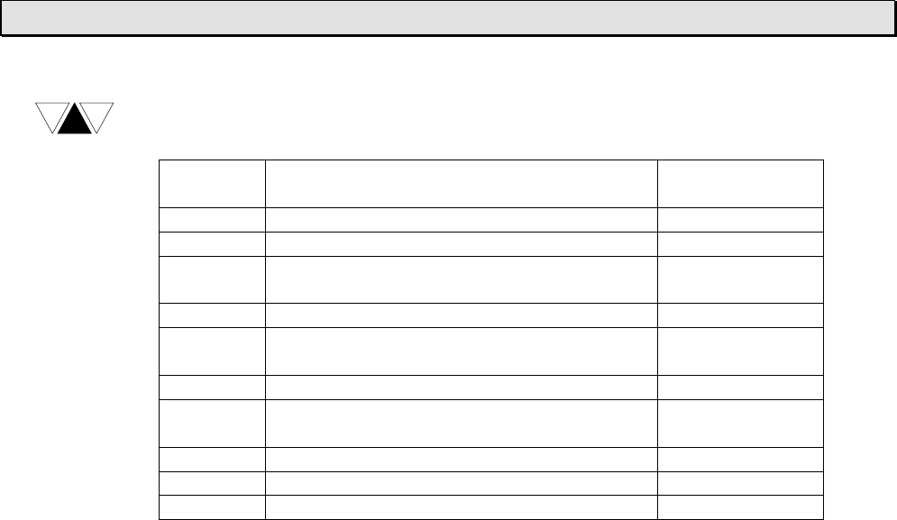
I/O status LEDs:
Indicates the ON/OFF status of each I/O signal. (color: red)
SW54 setting
value
I/O intending for an indication
Note
0 (default)
Basic unit (L: X000-007, H: Y020-027)
1
I/O module slot 0
2
I/O module slot 1
3
I/O module slot 2
4
I/O module slot 3
5
I/O module slot 4
6
I/O module slot 5
7
I/O module slot 6
8
I/O module slot 7
9
TOSLINE-F10 (FR112M), Low 1 word
10
TOSLINE-F10 (FR112M), High 1 word
It indicates these at the
time of only RUN
mode.
Others
Basic unit (L: X000-007, H: Y020-027)
Operation status LEDs:
Indicates the operation status of the T1-16S.
FLT
RUN
PWR
Lit
Internal 5 Vdc power is normal.
PWR
(Power) (green)
Not lit
Internal 5 Vdc power is not normal.
Lit
RUN mode (in operation)
Blinking
HOLD mode
RUN (green)
Not lit
HALT mode or ERROR mode
Lit
ERROR mode
Blinking
Hardware error (programmer cannot be connected)
FLT
(Fault) (red)
Not lit
Normal
Mode control switch:
Controls the operation modes of the T1-16S.
H (HALT)
When the switch is turned to H (HALT) side, the T1-16S stops
program execution (HALT mode). In this position, RUN/HALT
command from the programmer is disabled.
R (RUN)
When the switch is turned to R (RUN) side, the T1-16S starts
program execution. This is the position during normal operation.
In this position, RUN/HALT command from the programmer is also
available.
6F3B0253
24 T1-16S User’s Manual
1. System Configuration
Analog setting adjusters:
Two analog setting adjusters are provided. The V0 value is stored in SW30 and the
V1 value is stored in SW31. The converted value range is 0 to 1000. Refer to section
8.5 for details of the analog setting function.
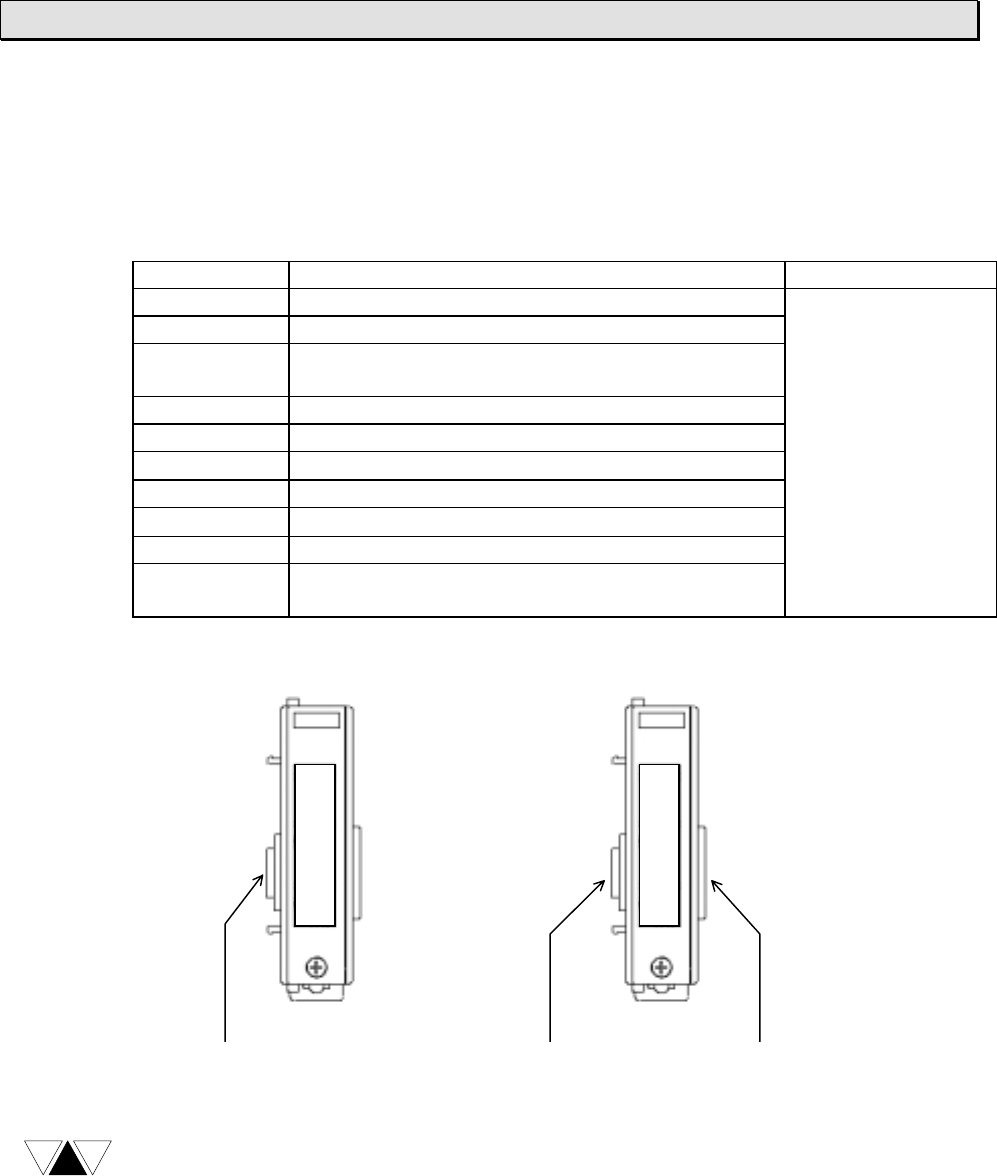
Programmer port connector:
Used to connect the programmer cable. The interface is RS-232C. This port can also
be used for the computer link function. Refer to section 1.6 for more information
about the computer link function.
Expansion connector:
Used to connect the I/O module.
RS-485 port (Enhanced model only):
Used to connect a computer (SCADA system), operator interface unit, other T1-16S,
or many kinds of serial ASCII devices including Toshiba’s Inverter through RS-485
interface. Refer to section 1.7 for more information about the T1-16S’s RS-485 multi-
purpose communication functions.
Mounting holes:
Used to fix the T1-16S on a mounting frame by screws. The mounting holes are
provided at two opposite corners.
Use two M4 screws for mounting. See section 4.2 for
installing the unit.
DIN rail bracket:
The DIN rail bracket is provided at the rear for mounting the T1-16S on a 35 mm DIN
rail. See section 4.2 for installing the unit.
T1
6F3B0253
Basic Hardware and Function 25
1. System Configuration
1.5.2 I/O modules
The T1-16S can connect up to eight I/O modules.
The following 10 types of the I/O modules are available.
For specification details of the I/O modules, refer to the separate manual “T1-16S
User’s Manual − I/O Modules −“.
Type
Description
Power supply
DI116M
16 points input, 24Vdc – 5mA
DO116M
16 points output, 24Vdc – 100mA
DD116M
8 points input, 24Vdc - 5mA
+ 8 points output, 24Vdc – 100mA
RO108M
8 points relay output, 24Vdc/240Vac - 1A
AD121M
1 channel analog input, 0 to 5V / 0 to 20mA
AD131M
1 channel analog input, ±10V
DA121M
1 channel analog output, 0 to 20mA
DA131M
1 channel analog output, ±10V
TC111M
1 channel thermo-couple input
FR112M
TOSLINE-F10 remote station,
1 word input + 1 word output
Supplied from the
basic unit (5 Vdc)
Expantion connector Expantion connectors
FR112M Other I/O modules
(1) If more than 8 I/O modules are connected, T1-16S cannot operate normally.
(2) The TOSLINE-F10 remote station module (FR112M) must be connected at the
right end. Tow or more FR112Ms cannot be used together.
NOTE

6F3B0253
26 T1-16S User’s Manual
1. System Configuration
1.5.3 Options
The following optional items are available.
Item
Type
Description
Cable for
programming tool
CJ105
For T-PDS, 5 m length
Programmer port
connector
PT16S
For RS-232C computer link, with 2 m cable
PT15S
Soldering type
Option card I/O
connector
PT15F
Cable side connector for
DI116M, DO116M, or DD116M
Flat cable type
Back-up battery
CR2032
For memory back up. (Available on the market.)
6F3B0253
Basic Hardware and Function 27
1. System Configuration
1.6 Programmer port function
The interface of the T1-16S’s programmer port is RS-232C. Normally this port is
used to connect the programmer. However, this port can also be used for the
computer link function.
The computer link is a data communication function between computer or operator
interface unit and the T1-16S. The data in the T1-16S can be read and written by
creating simple communication program on the computer. The computer link protocol
of the T1-16S is published in “T1-16S User’s Manual − Communication Function −”.
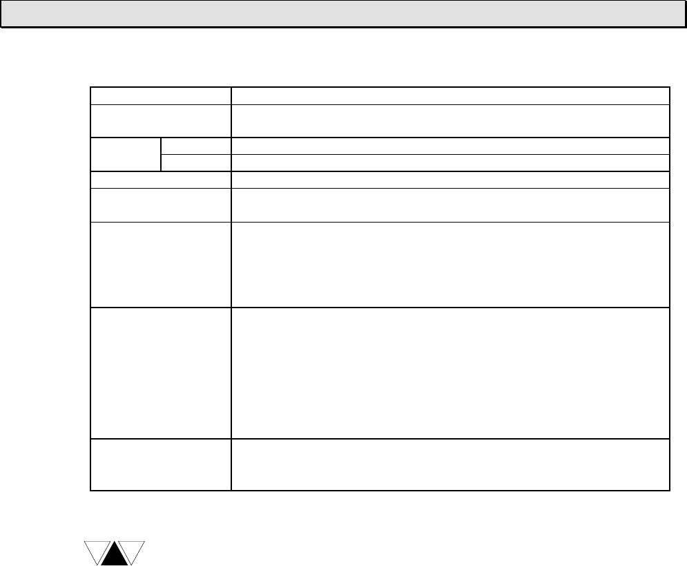
Item
Specifications
Interface
Conforms to RS-232C
Transmission system
Half-duplex
Synchronization
Start-stop system (asynchronous)
Transmission speed
9600 bps (fixed)
Transmission distance
15 m max.
Framing
Start bit:
Data bits:
Parity:
Stop bit:
1 bit
8 bits (fixed)
Odd or none
1 bit (fixed)
Protocol
T-series computer link (ASCII)
Programmer (binary)
Transmission delay option
0 to 300 ms
By using the multi-drop adapter (CU111), multiple T1-16Ss can be connected on an
RS-485 line. The T-series PLC programming software (T-PDS) can also be used in
this configuration.
T1-16S
C
U
Operator Interface Master Computer
RS-232C RS-485 (1 km max.) Max. 32 T1-16Ss
T1-16S
C
U
T1-16S
C
U
T1-16S
6F3B0253
28 T1-16S User’s Manual
1. System Configuration
1.7 RS-485 port communication function
The T1-16S enhanced model has an RS-485 multi-purpose communication port.
This port can work independent of the programmer port.
By using this communication port, one of the following four communication modes is
available, computer link mode, data link mode, free ASCII mode, and Inverter
connection mode.
For details of these functions, refer to the separate manual “T1-16S User’s Manual −
Communication Function −”.
Item
Computer
link
Free ASCII
Inverter
connection
Data link
Interface
Conforms to RS-458
Transmission system
Half-duplex
Synchronization
Start-stop system (asynchronous)
Transmission code
ASCII/binary
ASCII
Binary
Binary
Transmission speed
300, 600, 1200, 2400, 4800, 9600, or
19200 bps
19200 bps
(fixed)
Transmission
distance
1 km max.
Framing
Start bit: 1 bit
Data bits: 7 or 8 bits
Parity: Odd, even, or none
Stop bit: 1 or 2 bits
Special
Protocol
T-series
computer
link (ASCII),
Programmer
(binary)
User
defined
ASCII
messages
Inverter VF-
A7/G7/S9
binary
protocol
Special
Link configuration
1-to-N
N/A
1-to-N
1-to-1
T1-16S standard model does not have the RS-485 interface.
NOTE
6F3B0253
Basic Hardware and Function 29
1. System Configuration
Computer link mode
T-series computer link protocol can be used in this mode. A maximum of 32 T1-16Ss
can be connected to a master computer.
By using this mode, all the T1-16S’s data can be accessed by a master computer.
The T-series PLC programming software (T-PDS) can also be used in this
configuration.
Master Computer
RS-485 (1 km max.)
T1-16S T1-16S
T1-16S
Max. 32 T1-16Ss
T1-16S
Data link mode
Two PLCs (any combination of T1-16S, T2E or T2N) can be directly linked together.
This direct link is inexpensive, easily configured and requires no special
programming. Data registers D0000 to D0031 are used for the data transfer.
RS-485 (1 km max.)
Station No. 1
D0000
D0015
D0016
D0031
D0000
D0015
D0016
D0031
Station No. 2
T1
T1S
T1-16S
6F3B0253
30 T1-16S User’s Manual
1. System Configuration
Free ASCII mode
The free ASCII mode is used to connect between the T1-16S and various serial
ASCII devices, such as a micro computer, bar code reader, printer, display, etc.
By using this mode, the T1-16S can work as a communication master. Therefore, the
T1-16S can communicate with other PLCs using the computer link protocol.
• Bar-code reader
• ID system
• Weigh scale
• Power meter
• Printer
• Others
RS-485 (1 km max.)
T1-16S
6F3B0253
Basic Hardware and Function 31
1. System Configuration
Free ASCII mode
The T1-16S's Inverter connection mode is a special function to monitor/control the
Toshiba Inverters (ASDs) VF-A7/G7/S9 through the RS-485 line.
Using this mode, the T1-16S can perform the following functions for the Inverters
connected on the RS-485 line without any special communication program.
• Monitoring − Operating frequency and Terminal status
• Control − Run/Stop/Jog, Forward/Reverse, Frequency reference, etc.
• Parameter read/write
• Broadcast command
RS-485 (1 km max.)
VF-A7 VF-S9VF-A7
RS485 adapter
888
VF-S9
888
888 888
T1-16S
VF-S9 VF-S9
888 888
(Max. 64 Inverters)
6F3B0253
32 T1-16S User’s Manual
1. System Configuration
1.8 Real-time data link system
TOSLINE-F10
TOSLINE-F10 is a high speed data transmission system suited for small points I/O
distribution system. By inserting the TOSLINE-F10 remote module (FR112M), the
T1-16S can work as a remote station of the TOSLINE-F10 network. On this network,
the T1-16S sends 1 word data to the master station and receives 1 word data from
the master station.
Item
TOSLINE-F10 system specifications
High speed mode
Long distance mode
Topology
Bus (terminated at both ends)
Transmission distance
(without repeater)
500 m max. (total)
1 km max. (total)
Transmission speed
750 kbps
250 kbps
Scan transmission
capacity
512 points (32 words) max.
Scan cycle
7 ms/32 words
12 ms/32 words
Error checking
CRC check
Typical data link configuration
The figure below shows the typical data link configuration.
NOTE
T2E
(master)
T2E
(remote)
Master
computer
RI/O RI/O T1-16S
TOSLINE-F10
RI/O: remote I/O
Operator interface units
T1-16S T1-16S
(1) Refer to the separate “T1 User’s Manual − Option Card and I/O
Module −“ for details of the TOSLINE-F10 remote card (FR112).
(2) Refer to the separate TOSLINE-F10 User’s Manual for details of
overall TOSLINE-F10 system.

6F3B0253
Basic Hardware and Function 33
1. System Configuration
1.9 Peripheral tools
The following peripheral tools are available for the T1-16S.
T-Series Program Development System (T-PDS)
The T-Series Program Development System (T-PDS) is a software which runs on
any IBM-PC compatible personal computers such as Toshiba’s Notebook computers.
The same T-PDS software supports on-line/off-line programming, debugging and
program documentation for all the T-Series programmable controllers T1/T1S,
T2/T2E/T2N, T3/T3H and S2T.
• User-friendly program editor includes cut & paste, address search & replace,
program block move/copy, etc.
• Group programming − part program development by multiple designers and
merging them into a complete program − enhance the software productivity.
• Powerful monitoring, I/O force and data set functions fully support your program
debugging.
• Documentation of programs with commentary makes your maintenance work
easy.
• Remote monitoring/programming via modem (radio/phone) is possible.
The table below shows the T-PDS versions that support the T1-16S.
Type Part number Versions available for
T1-16/28/40 T1-40S/T1-16S
T-PDS for Windows TMW33E1SS Ver 1.0 or later *1) Ver 1.2 or later
T-PDS for MS-DOS TMM33I1SS Ver 1.61 or later *1) Ver 2.1 or later
*1) The T1-16S can be used with these versions. However, in this case, there are
the following functional limitations.
•The program size setting is only available as 2 k. It is set to 4 k mode in the
T1-16S.
•Some of the added instructions (MAVE, DFL, HTOA, ATOH) may not be
edited/monitored. (depending on the version)
NOTE
The connection cable for the T1-16S is different from that for upper T-Series
PLCs. These cables are supplied separately.
Connection cable for T1-16S ... Type: CJ105, 5 m length
Connection cable for T2/T3 …. Type: CJ905, 5 m length
6F3B0253
34 T1-16S User’s Manual
1. System Configuration
T-Series Handy Programmer (HP911A)
The HP911A is a hand-held programmer, that can be used to program the T1-16S
using ladder diagram. Its portability makes it ideal for maintenance use at remote
locations.
The HP911A has the following features.
• The HP911A supports ladder diagram programming of T-Series programmable
controllers T1-16S, T2/T2E/T2N and T3.
• Built-in EEPROM allows program copy between T-Series controllers.
• Two display modes are available,
- Normal: 5 lines and 12 columns
- Zoom: Full device description
• On-line data set and I/O force are useful for system checking.
• Backlit LCD display allows operation in dim light.
There are two types of the Handy Programmer (HP911) depending on the cable
included with.
Type Part number Cable included with Versions available for T1-16S
HP911A THP911A∗S2 m cable for T1-16S Ver 1.1 or later
HP911 THP911∗∗S2 m cable for the upper
T-series PLCs Ver 1.1 or later
The T1-16S can be used with the HP911(A). However, there are the following
functional limitations.
•The program size setting is only available as 2 k. It is set to 4 k mode in the T1-
16S.
•Some of the added instructions (MAVE, DFL, HTOA, ATOH) cannot be
edited/monitored.
NOTE A 2 m connection cable for the T1-16S (Type: CJ102) is supplied with the
HP911A. The cable for the T2/T3 is available separately. (Type: CJ902, 2 m
length)
6F3B0253
Basic Hardware and Function 35
1. System Configuration
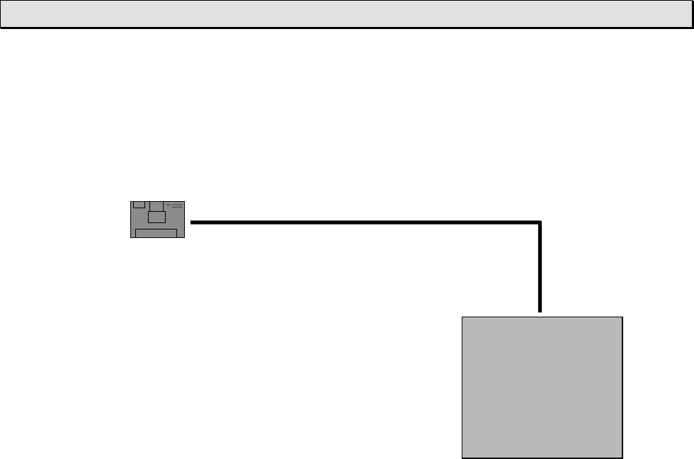
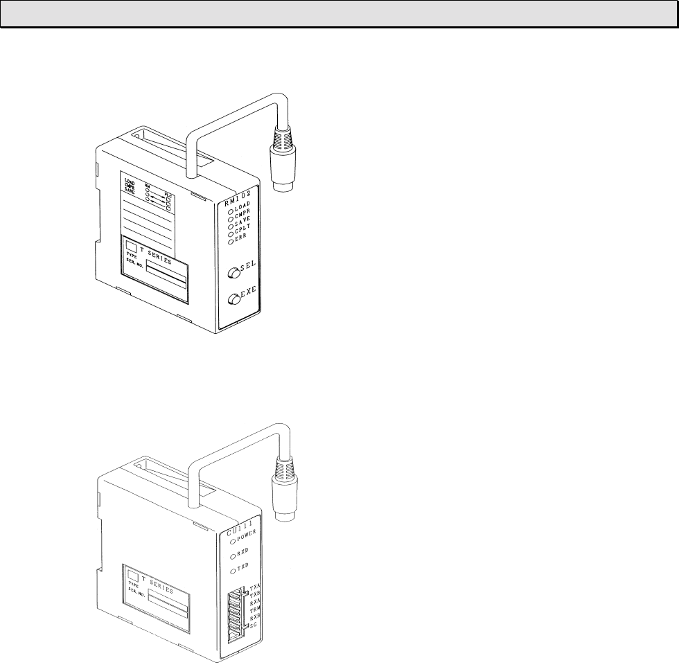
Program Storage Module (RM102)
The program storage module (RM102) is an
external memory for storing the T1-16S
program. By using the RM102, program saving
from the T1-16S to the RM102, and program
loading from the RM102 to the T1-16S can be
done without need of a programmer.
Because the RM102 has an EEPROM,
maintenance-free program storage and quick
saving/loading are available.
Multi-drop adapter (CU111)
The T1-16S’s RS-232C programmer port
supports the computer link function.
When two or more T1-16Ss are connected with
a master computer, the multi-drop adapter
(CU111) can be used. (One-to-N configuration)
The CU111 is an RS-232C/RS-485 converter
specially designed for the T1-16S’s
programmer port.
6F3B0253
36 T1-16S User’s Manual

6F3B0253
Basic Hardware and Function 37
Section 2
Specifications
2.1 General specifications, 38
2.2 Functional specifications, 40
2.3 I/O specifications, 42
2.4 External dimensions, 46

6F3B0253
38 T1-16S User’s Manual
2. Specifications
2.1 General specifications
Item T1-16S
Power supply voltage 100 to 240Vac (+10/-15%), 50/60 Hz
Power consumption 45VA or less
Inrush current 50A or less (at 240Vac, cold start)
24Vdc
(24Vdc, ±10%)
0.2A (for external devices and/or for input signals)
AC Power type
Output
rating
(Note) 5Vdc 1.5A (for I/O module)
Power supply voltage 24Vdc (+20/-15%)
Power consumption 18W or less
Inrush current 25A or less (at 24Vdc)
DC Power type
5Vdc output rating (Note) 1.5A (for I/O module)
Retentive power interruption 10ms or less
Insulation resistance 10MΩ or more
(between power terminals and ground terminal)
Withstand voltage 1500Vac - 1 minute
Ambient temperature 0 to 55°C (operation), -20 to 75°C (storage)
Ambient humidity 5 to 95%RH, no condensation
Noise immunity 1000Vp-p/1µs, Conform to EMC Directive 89/336/EEC
Vibration immunity 9.8m/s2 (1g)
(for 30 minutes per axis, on 3 mutually perpendicular axes)
Shock immunity 98m/s2 (10g)
(3 shocks per axis, on 3 mutually perpendicular axes)
Approximate weight 500g
(1) 24Vdc service power output is not provided on the DC power supply type.
(2) The maximum output current of the 5Vdc is 1.5A. However there is the following
restrictions, depending on the conditions.
• When HP911 is used:
→ Redused by 0.2A
• When RS-485 port is used:
→ Reduced by 0.1A
• When 24Vdc service power is used:
→ Refer to the right chart.
NOTE
24Vdc service power
5Vdc
maximum load current
0.2 (A)0.1
1.5
(A)
1.0
6F3B0253
Basic Hardware and Function 39
2. Specifications
(3) The 5Vdc current consumption of each I/O modules is described below.
Check that the total 5Vdc current consumption is within the limit.
Model Specifications 5Vdc consumer
current
DI116M 16points, 24Vdc-5mA input. 50mA
DO116M 16points, 24Vdc-100mA output. 50mA
DD116M 8points, 24Vdc-5mA input.
8points, 24Vdc-100mA output. 50mA
RO108M 8 points, 24Vdc/240Vac – 1A relay output 260mA
AD121M 1ch. 12bit analog input.
(0 to 20mA, 0 to 5V) 260mA
AD131M 1ch. 12bit analog input. (±10V) 260mA
DA121M 1ch. 12bit analog output.
(0 to 20mA, 0 to 5V) 350mA
DA131M 1ch. 12bit analog output. (±10V) 240mA
TC111M 1ch. 12bit thermo couple input. 400mA
FR112M TOSLINE-F10 remote station. 100mA
NOTE

6F3B0253
40 T1-16S User’s Manual
2. Specifications
2.2 Functional specifications
Item T1-16S
Control method Stored program, cyclic scan system
Scan system Floating scan or constant scan (10 – 200ms, 10ms units)
I/O update Batch I/O refresh
(direct I/O instruction available at basic unit’s I/O)
Program memory (Note) RAM and EEPROM (no back-up battery required)
Program capacity 8K steps
(4K or 8K mode)
Programming language Ladder diagram with function block
Instructions Basic: 21
Function: 97
Execution speed 1.4µs/contact, 2.3µs/coil,
4.2µs/16-bit transfer, 6.5µs/16-bit addition
1 main program
1 sub-program (initial program)
1 timer interrupt (interval: 5 to 1000ms, 5ms units)
4 I/O interrupt (high-speed counter and interrupt input)
Program types
256 subroutines (up to 3 levels of nesting)
I/O register 512 points/ 32 words (X/XW, Y/YW)
Auxiliary relay 4096 points/ 256 words (R/RW)
Special relay 1024 points/ 64 words (S/SW)
Timer 256 points (T./T)
64 at 0.01s, 192 at 0.1s
Counter 256 points (C./C)
Data register 4096 words (D)
User data
Index register 3 words (I, J, K)
Capacitor 1 hour (at 25°C)Memory
back-up Battery (option) Max. 2 years.
Min. 6 months. (Note)
(1) The user program stored in the EEPROM is transferred to the RAM
when power is turned on. Therefore, if the program is modified, it is
necessary to issue the EEPROM Write command from the programming
tool. Otherwise, the modified program is over-written by original
EEPROM contents at the next initial load timing.
(2) The data of RAM and calendar IC are backed up by built-in capacitor
and optional battery.
(3) When the optional battery is used, replace the battery periodically with
referring to the table below.
Annual average air temperature
Under 30°C (86°F) Over 30°C (86°F)
Over 8 hours 2 years 1 yearOperation
time per day Under 8 hours 1 year 6 months
NOTE
6F3B0253
Basic Hardware and Function 41
2. Specifications
Functional specifications (cont’d)
Item T1-16S
I/O capacity 16 points (basic)
+128 points (I/O modules)
Input 24Vdc input (8 points)I/O type Output Relay (6 points) + transistor (2 points)
I/O terminal block Fixed
Real-time clock
/calendar Yes, ±60 s/month at 25°C
(Enhanced model only)
Special I/O functions
(Note) • High speed counter, 2 single or 1 quadrature
• Interrupt input, 2 points
• Adjustable analog register, 2 points
• Pulse output, CW+CCW or pulse+direction
• PWM output
Communications
interface • 1 port RS-232C (programmer port)
- for Programmer or Computer link connection
• 1 port RS-485 (Enhanced model only)
- Programmer
- Computer link
- Data link
- Free ASCII
• TOSLINE-F10 remote (by I/O module)
Debug support
function • Sampling trace, 8 devices and 3 register - 256 times
• On-line programming
• On-line EEPROM write
(1) High-speed counter, interrupt input, pulse output and PWM output are
available in the DC input types.
(2) High-speed counter and interrupt input cannot be used simultaneously.
(3) Pulse output and PWM output cannot be used simultaneously.
NOTE
6F3B0253
42 T1-16S User’s Manual
2. Specifications
2.3 I/O specifications
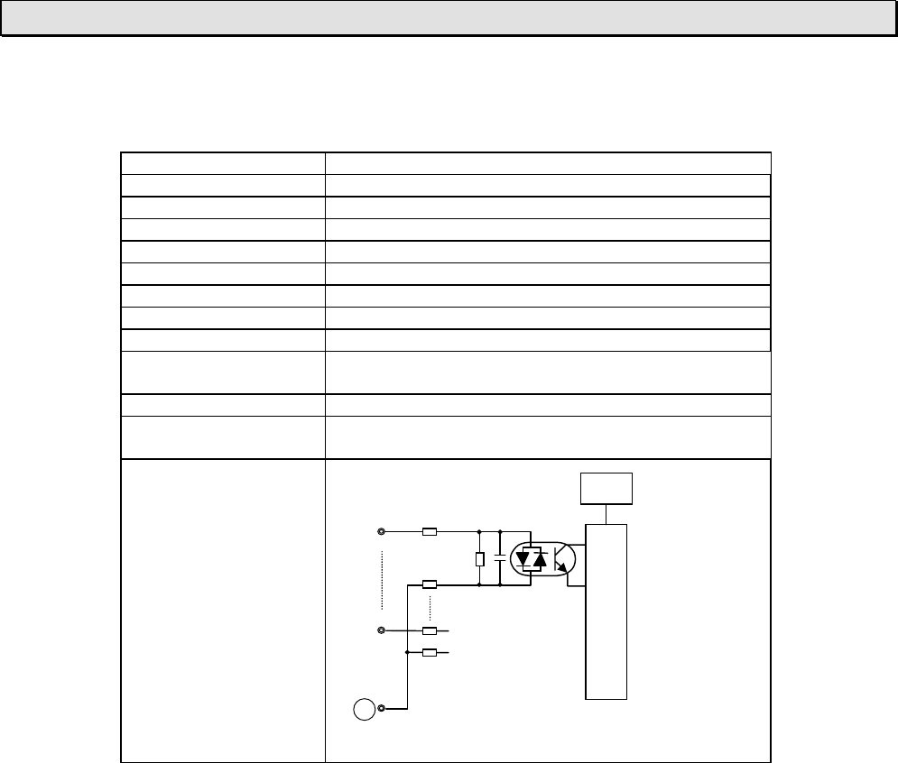
• Input specifications
Item Specifications
Input type DC input, current source/sink
Number of input points 8 points (8 points/common)
Rated input voltage 24Vdc, +10/-15 %
Rated input current 7mA (at 24Vdc)
Min. ON voltage 15Vdc
Max. OFF voltage 5Vdc
ON delay time 0 to 15ms *1
OFF delay time 0 to 15ms *1
Input signal display LED display for all points, lit at ON, internal logic
side
External connection Removable terminal block, M3
Withstand voltage 1500Vac, 1 minute
(between internal and external circuits)
Internal circuit
7
0
C
Internal circuit
LED
*1: User can change the input ON/OFF delay time of the DC input.
The setting range is 0 to 15ms. (Default value = 10ms) Refer to section 8.2.
6F3B0253
Basic Hardware and Function 43
2. Specifications
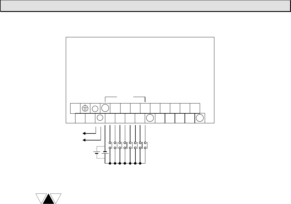
• Input signal connections
24Vdc
Service power
24Vdc
31
0
L
42
NCN
T1-16S
DC IN
−
+2422206
2321
Vin
75
26
2725
24Vdc input
C
C C
The 24Vdc service power output is not provided on the DC power supply type.
NOTE
6F3B0253
44 T1-16S User’s Manual
2. Specifications
• Output specifications
SpecificationsItem Relay output Transistor output
Output type Relay contact, normally open Transistor output, current sink
Number of output points 6 points
(6 pts/common) 2 points
(2 points/common)
Rated load voltage 240Vac/24Vdc (max.) 24Vdc
Range of load voltage Max. 264Vac/125Vdc 20.0 - 28.0Vdc
Maximum load current 2A/point (resistive),
4A/common 0.5A/point (resistive)
ON resistance 50mΩ or less
(initial value) −
Voltage drop at ON −0.5V or less
Leakage current at OFF None 0.1mA or less
Minimum load 5Vdc, 10mA
(50mW) −
ON delay time 10ms or less 0.1ms or less
OFF delay time 10ms or less 0.1ms or less
Input signal display LED display for all points, lit at ON, internal logic side
External connection Removable terminal block, M3
Withstand voltage 1500Vac, 1 minute (between internal and external circuits)
Internal circuit
Ry 22
27
Internal circuit
LED
C
Vin
21
Internal circuit
LED
C
20
*1: The switching life of the relay output is as follows.
20 million times or more (mechanical)
100 thousand times or more (electrical, at maximum rated voltage and current)
6F3B0253
Basic Hardware and Function 45
2. Specifications
• Output signal connections
24Vdc
Service power
24Vdc
3 1
0
L
4 2
NC
N
T1-16S
DC OUT
−
+ 24 22 20 6
23 21
Vin
7 5
26
27 25
C
C C
RELAY OUT
PS
+
Transister output
Relay output
PS 240Vac/24Vdc (max.)
6F3B0253
46 T1-16S User’s Manual
2. Specifications
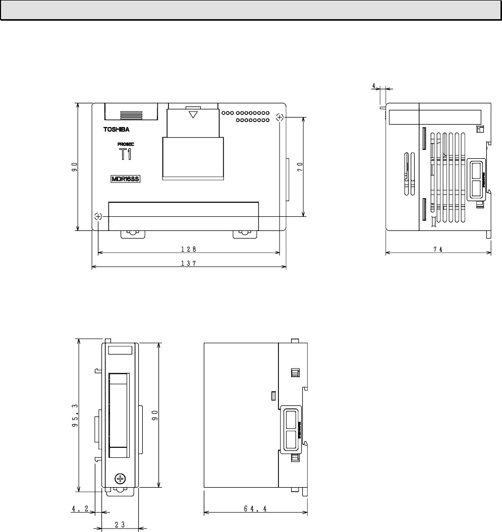
2.4 External dimensions
♦ T1-16S
[mm]
♦ I/O module
[mm]

6F3B0253
Basic Hardware and Function 47
Section 3
I/O Application Precautions
3.1 Application precautions for input signals, 48
3.2 Application precautions for output signals, 50
6F3B0253
48 T1-16S User’s Manual
3. I/O Application Precautions
3.1 Application precautions for input signals
(1) Minimum ON/OFF time of the input signal
The following conditions guarantee correct reading of the ON/OFF state of the input
signal:
Input ON time: ON delay time + the time for one scan
Input OFF time: OFF delay time + the time for one scan
The ON and OFF times of the input signals must be longer than these intervals.
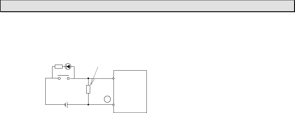
(2) Increasing the contact current
The reliability of some contacts cannot be guaranteed by the specified input current. In
this case, install an external bleeder resistor to increase the contact current.
T1
input
circuit
I1 I
Bleeder resistor
R
V
I2
RV
II
Wattage V
R
=−
>×
1
23
(3) Connecting transistor output device
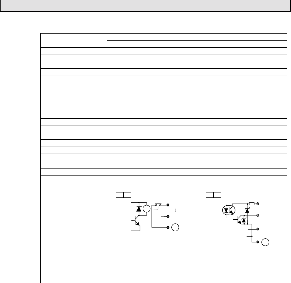
An example of connecting a transistor output device to T1-16S’s input circuit is shown
below.
• For NPN open collector • For PNP open collector
C
T1
input
circuit
T1
input
circuit
C
!WARNING Configure emergency stop and safety interlocking circuits outside the
T1-16S. Otherwise, malfunction of the T1-16S can cause injury or serious
accidents.
6F3B0253
Basic Hardware and Function 49
3. I/O Application Precautions
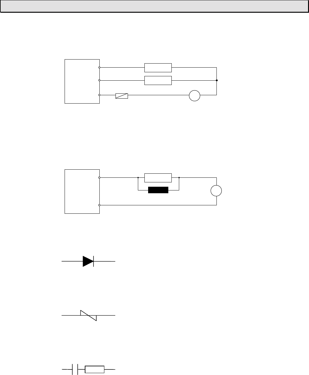
(4) Countermeasures against leakage current
When a switch with an LED or sensor is used, the input sometimes cannot recognize
that the switch is off due to the current leakage. In this case, install a bleeder resistor
to reduce input impedance.
Select a bleeder resistor according to the following criteria:
(a) The voltage between the input terminals must be lower than the OFF voltage
when the sensor is switched off.
(b) The current must be within the allowable range when the sensor is switched on.
(c) Calculate the wattage of the bleeder resistor by multiplying the current when the
sensor is switched on times three.
T1
input
circuit
Bleeder resistor
LE
C

6F3B0253
50 T1-16S User’s Manual
3. I/O Application Precautions
3.2 Application precautions for output signals
(1) 2 points of solid-state output
The leading 2 points of output (Y020 and Y021) are solid-state outputs, transistors on
the DC input types.
These solid-state outputs are suited for frequent switching applications.
Note that the specifications of the solid-state outputs and other outputs (relays) are
different.
(2) Switching life of output relays
Expected relay life is more than 100,000 electrical cycles at rated maximum voltage
and current, and more than 20 million mechanical cycles. The expected contact life
(electrical cycles) is shown on the table below.
Load
voltage Load
current Expected life
(thousand) Load
voltage Load
current Expected life
(thousand)
AC 110Vac, 2A 340 DC 24Vdc, 2A 280
load COSφ = 1 1A 720 load L/R = 0 ms 1A 600
0.5A 1,600 0.5A 1,300
110Vac, 2A 150 24Vdc, 2A 60
COSφ = 0.7 1A 320 L/R = 15 ms 1A 150
0.5A 700 0.5A 350
220Vac, 2A 220 48Vdc, 1A 200
COSφ = 1 1A 500 L/R = 0 ms 0.5A 420
0.5A 1,100 48Vdc, 0.5A 130
220Vac, 2A 100 L/R = 15 ms 0.2A 420
COSφ = 0.7 1A 210 110Vdc, 0.5A 200
0.5A 460 L/R = 0 ms 0.2A 550
110Vdc, 0.2A 150
L/R = 15 ms 0.1A 350
!
WARNING
!
CAUTION
Configure emergency stop and safety interlocking circuits outside the
T1-16S. Otherwise, malfunction of the T1-16S can cause injury or serious
accidents
1. Turn on power to the T1-16S before turning on power to the loads.
Failure to do so may cause unexpected behavior of the loads.
2. Configure the external circuit so that the external 24Vdc power required
for the transistor output circuits and power to the loads are switched
on/off simultaneously. Also, turn off power to the loads before turning off
power to the T1-16S.
3. Install fuses appropriate to the load current in the external circuits for the
outputs. Failure to do so can cause fire in case of load over-current.
6F3B0253
Basic Hardware and Function 51
3. I/O Application Precautions
(3) Over-current protection
The output circuit of the T1-16S does not contain protective fuses. Fuses rated for the
output should be provided by the user.
(4) Output surge protection
Where an inductive load is connected to the output, a relatively high energy transient
voltage will be generated when the relay turns OFF. To prevent the problems caused
by this surge, install a surge absorber in parallel to the inductive load.
Surge absorber:
• Flywheel diode (for DC output)
Inverse withstand voltage: At least three times that of the power supply
Forward current: Larger than the load current
• Varistor (for AC output)
The voltage rating is 1.2 times the maximum (peak) voltage of the power supply
• CR snubber (for DC or AC output)
R: 0.5 to 1Ω per volt coil voltage
C: 0.5 to 1µF per ampere of coil current (non-polarity capacitor)
T1
output
PS
Load
Load
Fuse appropriate to
the common current
T1
output
circuit
PS
Load
Surge absorber
6F3B0253
52 T1-16S User’s Manual

6F3B0253
Basic Hardware and Function 53
Section 4
Installation and Wiring
4.1 Environmental conditions, 54
4.2 Installing the unit, 55
4.3 Wiring terminals, 57
4.4 Grounding, 58
4.5 Power supply wiring, 59
4.6 I/O wiring, 61

6F3B0253
54 T1-16S User’s Manual
4. Installation and Wiring
4.1 Environmental conditions
Do not install the T1-16S in the following locations:
• Where the ambient temperature drops below 0°C or exceeds 55°C.
• Where the relative humidity drops below 20% or exceeds 90%.
• Where there is condensation due to sudden temperature changes.
• In locations subject to vibration that exceeds tolerance.
• In locations subject to shock that exceeds tolerance.
• Where there are corrosive or flammable gases.
• In locations subject to dust, machining debris or other particles.
• In locations exposed to direct sunlight.
Observe the following precautions when installing enclosures in which the T1-16S will
be installed:
• Provide the maximum possible distance from high-voltage or high-power panels.
This distance must be at least 200mm.
• If installing the enclosures in the vicinity of high-frequency equipment, be sure to
correctly ground the enclosures.
• When sharing the channel base with other panels, check for leakage current from
the other panels or equipment.
!
CAUTION
Excess temperature, humidity, vibration, shocks, or dusty and corrosive
gas environment can cause electrical shock, fire or malfunction.
Install and use the T1-16S and related equipment in the environment
described in this section.
6F3B0253
Basic Hardware and Function 55
4. Installation and Wiring
4.2 Installing the unit
The T1-16S basic unit and the I/O module come equipped with a bracket at the rear
for mounting on a 35mm DIN rail.
Installation precautions:
• Because the T1-16S is not dust-proof, install it in a dust-proof enclosure.
• Do not install the unit directly above equipment that generates a large amount of
heat, such as a heater, transformer, or large-capacity resistor.
• Do not install the unit within 200mm of high-voltage or high-power cables.
• Allow at least 70mm on all sides of the unit for ventilation.
• For safely during maintenance and operation, install the unit as far as possible from
high-voltage or power equipment. Alternatively, keep the unit separate using a
metal plate or similar separator.
• If high-frequency equipment is installed in the enclosure together with the T1-16S,
special attention is required for grounding. See section 4.4.
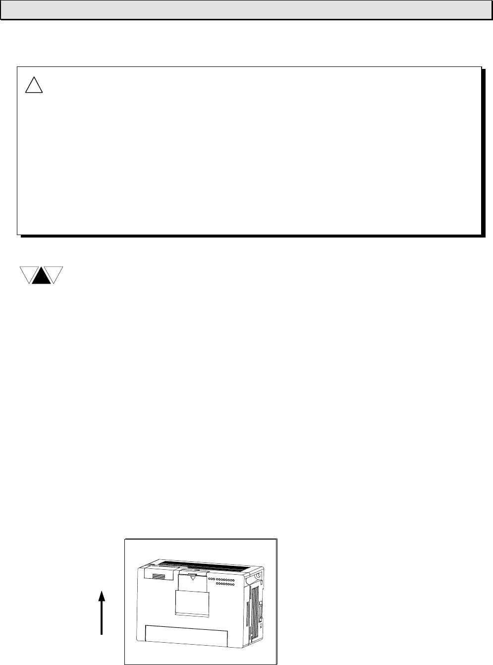
• Be sure to install the unit vertically with keeping the power terminals downside. Do
not install the unit horizontally or upside-down for safety reason.
• Use M4 size screws to mount the T1-16S.
(Recommended torque: 1.47N⋅m = 15Kgf⋅cm)
!
CAUTION
NOTE
1. Improper installation directions or insufficient installation can cause
fire or the units to drop. Install the T1-16S and related equipment in
accordance with the instructions described in this section.
2. Turn off power before installing or removing any units, modules,
racks or terminal blocks. Failure to do so can cause electrical shock
or damage to the T1-16S and related equipment.
3. Entering wire scraps or other foreign debris into to the T1-16S and
related equipment can cause fire or malfunction. Pay attention to
prevent entering them into the T1 and related equipment during
installation and wiring.
Mount the T1-16S on a vertical panel.
All other mounting positions are not
acceptable.
Upward
6F3B0253
56 T1-16S User’s Manual
4. Installation and Wiring
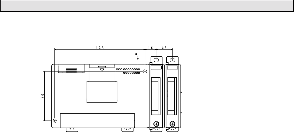
Dimensions for screw mounting:
6F3B0253
Basic Hardware and Function 57
4. Installation and Wiring
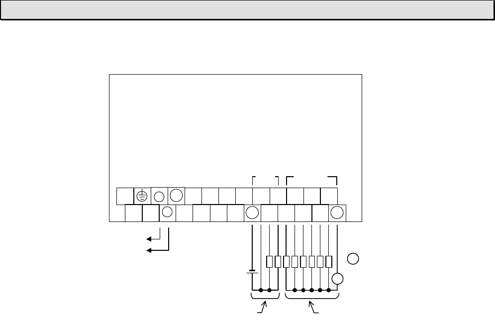
4.3 Wiring terminals
The terminal screw size of the T1-16S is M3. Use crimp-style terminals of 7mm width
or less useable for M3. The terminal block is not removable (fixed).
For input and output signal connections, refer to sections 2.4 and 3.
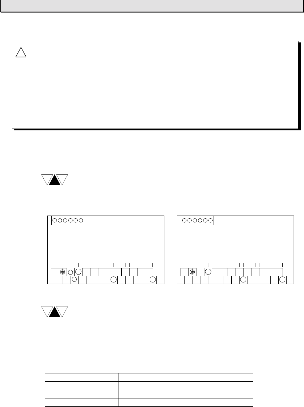
T1-MDR16SS .... AC power supply model T1-MDR16SSD..DC power supply model
3 1
0
L
4 2
NC
N
MDR16SS
DC OUT
−
+ 24 22 20 6
23 21
Vin
7 5
26
27 25
C
C C
RELAY OUT DC IN
RS-485 (Enhanced model only)
3 1
0
+
4 2
NC
-
MDR16SSD
DC OUT
NC
NC 24 22 20 6
23 21
Vin
7 5
26
27 25
C
C C
RELAY OUT DC IN
RS-485 (Enhanced model only)
TXA RXA RXB
TXB TRM SG TXA RXA RXB
TXB TRM SG
(1) NC stands for ”no connect”. Do not use the NC terminals for wire
relaying or branching.
(2) For the connections of the RS-485 communication port (the upper
terminal block), refer to the separate manual “T1-16S User’s Manual -
Communication Function -.
The applicable wire size is 0.3mm2 (22 AWG) to 1.25mm2 (16 AWG). The table below
shows the recommended wire size.
Type of signal Recommended wire size
Power 1.25mm2 (16 AWG)
Grounding 1.25mm2 (16 AWG)
I/O signals 0.3mm2 (22 AWG) to 0.75mm2 (18 AWG)
!
CAUTION
1. Turn off power before wiring to minimize the risk of electrical shock.
2. Exposed conductive parts of wire can cause electrical shock. Use
crimp-style terminals with insulating sheath or insulating tape to cover
the conductive parts. Also close the terminal covers securely on the
terminal blocks when wiring has been completed.
3. Turn off power before removing or replacing units, modules, terminal
blocks or wires. Failure to do so can cause electrical shock or damage
to the T1-16S and related equipment.
NOTE
NOTE
6F3B0253
58 T1-16S User’s Manual
4. Installation and Wiring
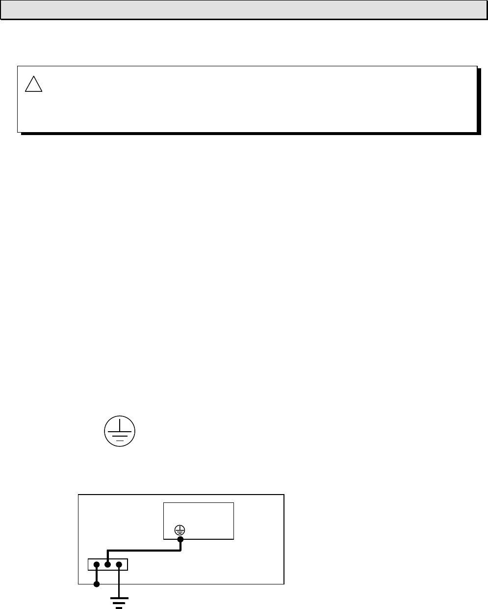
4.4 Grounding
The optimum method for grounding electronic equipment is to ground it separately
from other high-power systems, and to ground more than one units of electronic
equipment with a single-point ground.
Although the T1-16S has noise immunity to be used in industrial operating conditions,
grounding is important for safety and reliability.
Check the grounding against the following criteria.
1. The T1-16S must not become a path for a ground current. A high-frequency current
is particularly harmful.
2. Equalize the ground potentials when the expansion rack or unit is connected.
Ground the T1-16S and the expansion rack or unit at a single point.
3. Do not connect the ground of the T1-16S to that of high-power systems.
4. Do not use a ground that has unstable impedance, such as painted screws, or
ground subject to vibration.
The grounding marked terminal (see below) is provided on the T1-16S basic unit for
grounding purpose.
In case of the expansion rack is connected to the T1-16S, the rack mounting screw is
used for this purpose.
System ground
T1-16S
Mounting panel
• 1.25mm2 (16 AWG) wire should be used to connect the T1-16S and the expansion
rack/unit with the enclosure grounding bus bar.
• 100Ω or less to ground is required.
!CAUTION 1. Turn off power before wiring to minimize the risk of electrical shock.
2. Operation without grounding may cause electrical shock or malfunction.
Connect the ground terminal on the T1-16S to the system ground.
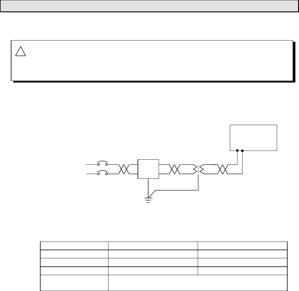
6F3B0253
Basic Hardware and Function 59
4. Installation and Wiring
4.5 Power supply wiring
Wire the power source to the T1-16S power supply terminals.
Insulation
transformer
Line filter
Power source
T1-16S
• Power conditions:
AC power supply type DC power supply type
Rated voltage 100 to 240Vac, +10/-15% 24Vdc, +20/-15%
Frequency 50/60Hz, ±5% -
Power consumption 45VA or less 18W or less
Retentive power
interruption Continuous operation for less than 10ms
• 1.25mm2 (16 AWG) twisted-pair cable should be used for the power cable.
• The power cable should be separated from other cables.
!CAUTION 1. Turn off power before wiring to minimize the risk of electrical shock.
2. Applying excess power voltage to the T1-16S can cause explosion or
fire. Apply power of the specified ratings described below.
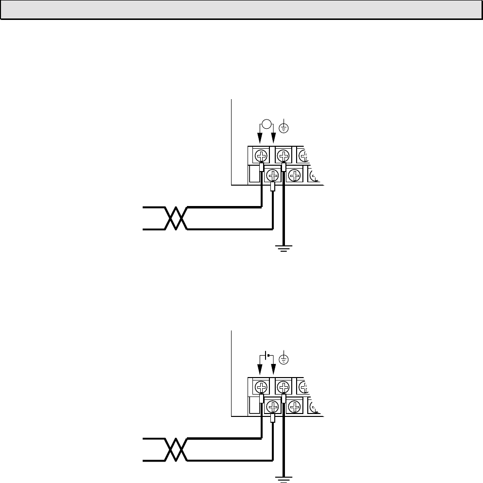
6F3B0253
60 T1-16S User’s Manual
4. Installation and Wiring
Connections of the power supply terminals are shown below.
• AC power supply type
100 to 240Vac
Grounding
N
L
∼
100-240Vac
• DC power supply type
24Vdc
Grounding
-
+
24 Vdc
+
-
6F3B0253
Basic Hardware and Function 61
4. Installation and Wiring
4.6 I/O wiring
• Refer to sections 2.4 and 3 for instructions on how to properly wire the I/O
terminals.
• 0.75mm2 (18 AWG) to 0.3mm2 (22 AWG) wires are recommended for I/O signals.
• Separate the I/O signal cables from high-power cables by at least 200mm.
• If expansion rack or unit is used, separate the expansion cable from the power and
I/O signal cables by or unit at least 50mm.
• It is recommended to separate the input signal cables from output signal cables.
T1-16S 200mm
or more
High-power
cable
Output
signal
Input
signal
!CAUTION 1. Turn off power before wiring to minimize the risk of electrical shock.
2. Exposed conductive parts of wire can cause electrical shock. Use
crimp-style terminals with insulating sheath or insulating tape to cover
the conductive parts. Also close the terminal covers securely on the
terminal blocks when wiring has been completed.
3. Turn off power before removing or replacing units, modules, terminal
blocks or wires. Failure to do so can cause electrical shock or damage
to the T1-16S and related equipment.
6F3B0253
62 T1-16S User’s Manual

6F3B0253
Basic Hardware and Function 63
Section 5
Operating System Overview
5.1 Operation modes, 64
5.2 About the built-in EEPROM, 66
5.3 Scanning, 69

6F3B0253
64 T1-16S User’s Manual
5. Operating System Overview
5.1 Operation modes
The T1-16S has three basic operation modes, the RUN mode, the HALT mode and
the ERROR mode. The T1-16S also has the HOLD and RUN-F modes mainly for
system checking.
RUN: The RUN mode is a normal control-operation mode.
In this mode, the T1-16S reads external signals, executes the user program
stored in the RAM, and outputs signals to the external devices according to
the user program. It is in the RUN mode that the T1-16S performs scans the
user program logic, which is the basic operation of a PLC.
Program changes and EEPROM write are possible while the T1-16S is in
the RUN mode. Refer to section 6.9.
HALT: The HALT mode is a programming mode.
In this mode, user program execution is stopped and all outputs are
switched off.
Program loading into the T1-16S is possible only in the HALT mode.
For the standard T1, program changes and EEPROM write are possible only
when the T1 is in the HALT mode.
ERROR: The ERROR mode is a shutdown mode as a result of self-diagnosis.
The T1-16S enters the ERROR mode if internal trouble is detected by self-
diagnosis. In this mode, program execution is stopped and all outputs are
switched off. The cause of the shutdown can be confirmed by connecting
the programming tool.
To exit from the ERROR mode, execute the Error Reset command from the
programming tool, or cycle power off and then on again.
HOLD: The HOLD mode is provided mainly for checking the external I/O signals.
In this mode, user program execution is stopped, with input and output
updating is executed. It is therefore possible to suspend program execution
while holding the output state. Moreover, a desired output state can be
established by setting any data by using the programming tool.
RUN-F: The RUN-F mode is a forced RUN mode provided for program checking.
This mode is effective when using the expansion I/Os.
Deferent from the normal RUN mode, the RUN-F mode allows operation
even if the registered I/O modules are not actually mounted.
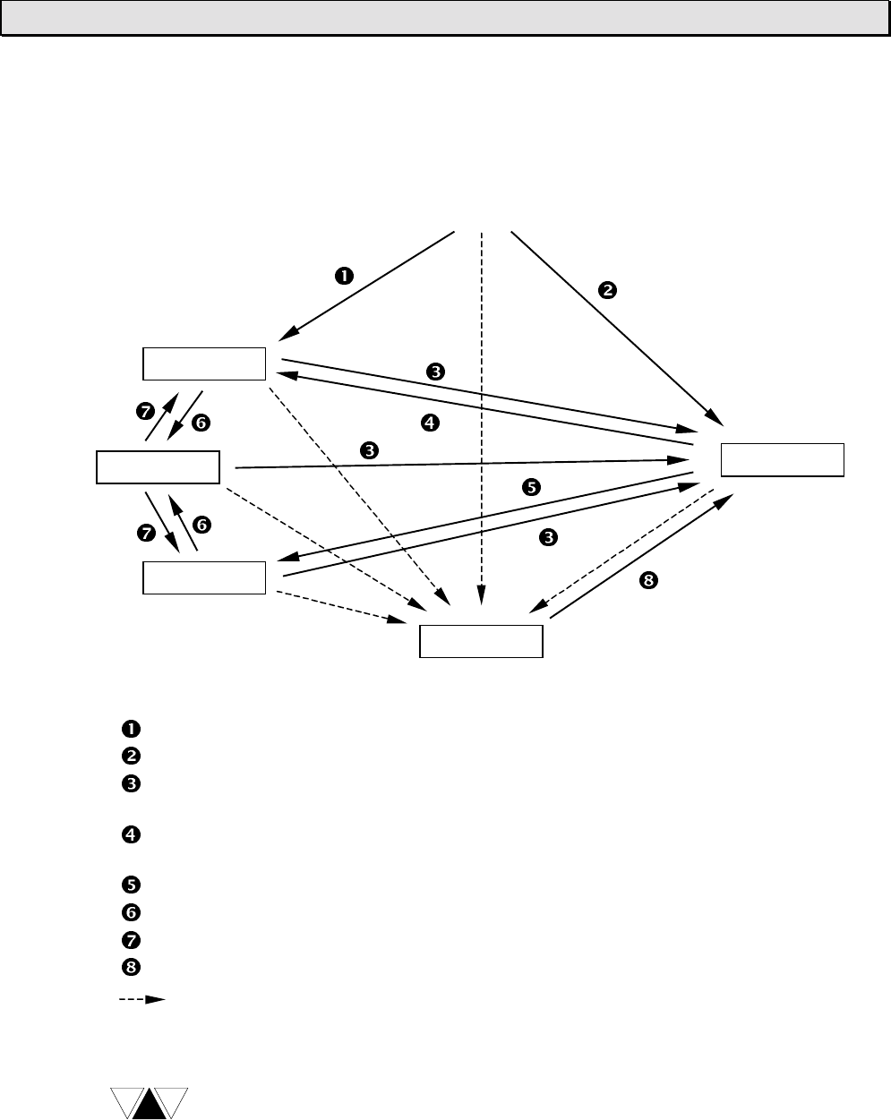
6F3B0253
Basic Hardware and Function 65
5. Operating System Overview
The operation modes are switched by the mode control switch provided on the T1-16S
and the mode control commands issued from the programming tool.
The mode transition conditions are shown below.
Mode control switch is in R (RUN) side.
Mode control switch is in H (HALT) side.
Mode control switch is turned to H (HALT) side, or HALT command is issued from
the programming tool.
Mode control switch is turned to R (RUN) side, or RUN command is issued from
the programming tool.
Force RUN (RUN-F) command is issued from the programming tool.
HOLD command is issued from the programming tool.
HOLD Cancel command is issued from the programming tool.
Error Reset command is issued from the programming tool.
(dotted line) Error is detected by self-diagnosis.
The commands from the programming tool are available when the mode
control switch is in R (RUN) side.
(Power ON)
RUN
HALT
HOLD
RUN-F
ERROR
NOTE

6F3B0253
66 T1-16S User’s Manual
5. Operating System Overview
5.2 About the built-in EEPROM
The T1-16S is equipped with a built-in EEPROM and a RAM as standard features.
The user program is stored in the EEPROM so that the user program can be
maintained without the need of a battery. A part of the Data register can also be
stored in the EEPROM.
The table below shows the contents stored in the built-in EEPROM.
T1-16S
User program Entire program (8 k steps) and System information
User data User specified number of Data register starting with address 0.
It is set by SW55.
D0000 - Dnnnn
(up to 2048 words)
Setting
information SW36 - SW38:
Programmer port settings
SW55:
Number of Data register to be saved in the EEPROM
SW56 - SW57:
RS-485 port settings
Sampling trace setting information
The user program and the data stored in the EEPROM are transferred to the RAM
when power is turned on. Subsequent program execution is done based on the RAM
contents. Program editing is also performed on the RAM contents.
Therefore, if the program is modified, it is necessary to issue the EEPROM Write
command from the programming tool. Otherwise, the modified program is over-
written by original EEPROM contents when the power is turned off and on again.
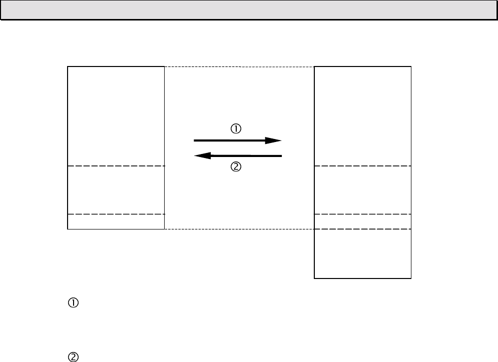
6F3B0253
Basic Hardware and Function 67
5. Operating System Overview
EEPROM
User program
(8 k steps)
and System info
User program
(8 k steps)
and System info
Data register
(D0000 to Dnnnn,
user setting)
Data register
(0 to 2048 words,
user setting)
Other dataOther data
RAM
The rest of Data
register and
other registers
Executed when power is turned on (it is called initial load) or EEPROM Read
command is issued from the programming tool. The EEPROM Read is possible
only in the HALT mode.
Executed when EEPROM Write command is issued from the programming tool.
It is possible in either HALT or RUN mode. (See Note)
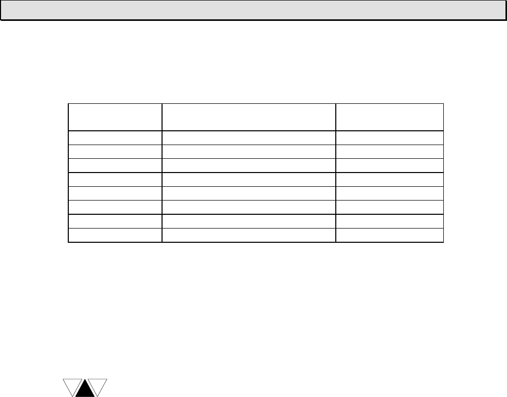
6F3B0253
68 T1-16S User’s Manual
5. Operating System Overview
Special register SW55 is used to specify the number of Data registers to be stored in
the EEPROM. The allowable setting value is 0 to 2048.
The table below shows the correspondence between the SW55 value and Data
registers saved in the EEPROM.
SW55 setting
value Range of Data registers saved
in EEPROM Remarks
0 None
1 D0000 only
2 D0000 to D0001
3 D0000 to D0002
::
2047 D0000 to D2046
2048 D0000 to D2047 Default value
Others D0000 to D2047 Regarded as 2048
When the EEPROM Write command is executed, the T1-16S checks the value of
SW55 and saves the Data registers into the EEPROM depending on the SW55 value.
The value of SW55 itself is also saved in the EEPROM.
At the initial load or the EEPROM Read command is executed, the T1-16S checks the
value for SW55 in the EEPROM and transfers the corresponding number of data to
the Data registers of the RAM.
(1) The EEPROM has the life limit for writing. It is 100,000 times. Pay
attention not to exceed the limit. If the number of execution of
EEPROM Write command exceeds 100,000 times, EEPROM alarm
flag (S007) comes ON.
(2) Even in RUN mode, the EEPROM Write command can be executed.
However, in this case, only the user program is written into the
EEPROM. (D register data and setting information are not saved.)
(3) The data in the EEPROM can also be read or written by using the
program instruction (FUN236 XFER instruction).
(4) When the EEPROM writing is executed by the XFER instruction in the
user program, T1-16S does not update the internal EEPROM write
counts. Therefore the EEPROM alarm flag (S007) will not correspond
to this operation. Pay attention to the life limit of the EEPROM.
NOTE
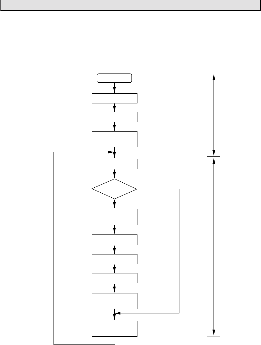
6F3B0253
Basic Hardware and Function 69
5. Operating System Overview
5.3 Scanning
The flowchart below shows the basic internal operations performed by the T1-16S
from the time power is turned on through program execution. As the diagram shows,
executing a program consists of continuous scanning operations. One scan is a cycle
starting with the self-diagnosis and ending with the completion of peripheral support.
Power ON
Hardware check
Initial load
Self-diagnosis
Register/device
initialization
Mode
control
Register/device
initialization
Program check
I/O update
Timer update
User program
execution
Peripheral
support
Power-up
Initialization
(approx. 1 s)
HALT mode
Scan cycle
RUN mode
At the first
scan
At the first
scan
Scan
6F3B0253
70 T1-16S User’s Manual
5. Operating System Overview
Hardware check:
Performs checking and initialization of the system ROM, the system RAM and the
peripheral LSIs.
Initial load:
Transfers the user program and user data from the EEPROM to the RAM. (Refer to
section 5.2)
Register/device initialization:
Initializes registers and devices as shown below.
Register/device Initialization
External input (X/XW) Forced inputs are retained. Others are cleared to 0.
External output (Y/YW) Forced coil devices are retained. Others are cleared to 0.
Auxiliary device/register
(R/RW) User specified retentive registers and forced coil devices
are retained. Others are cleared to 0.
Special device/register
(S/SW) Special setting data are retained. Others are cleared to 0.
Timer device/register
(T./T) User specified retentive registers are retained. Others are
cleared to 0.
Counter device/register
(C./C) User specified retentive registers are retained. Others are
cleared to 0.
Data register (D) User specified retentive registers are retained. Others are
cleared to 0.
Index register (I, J, K) Cleared to 0.
(1) When the data stored in the EEPROM (Data registers) are used, these
registers should be specified as retentive. Otherwise, these data are
transferred from EEPROM to RAM, but then cleared to 0 at the
initialization.
(2) The data in the retentive registers are stored in RAM and backed up by
built-in capacitor and by the optional battery if used. The back-up
period is 1 hours or more at 25 °C. If optional battery (CR2032) is
used, the back-up period is 1 year or more at 25 °C.
The T1-16S checks the validity of the retentive data at the power-up
initialization, and if they are not valid, sets the special device (S00F) to
ON. Therefore, check the status of S00F in the user program and
initialize the retentive registers if S00F is ON.
(3) The retentive registers can be set by the programming tool for RW, T,
C and D registers. The registers from address 0 to the designated
address for each type are set as retentive registers. Refer to the
separate manual for the programming tool for setting the retentive
registers.
(4) The input force and the forced coil are functions for program
debugging. For details, refer to section 6.7.
NOTE
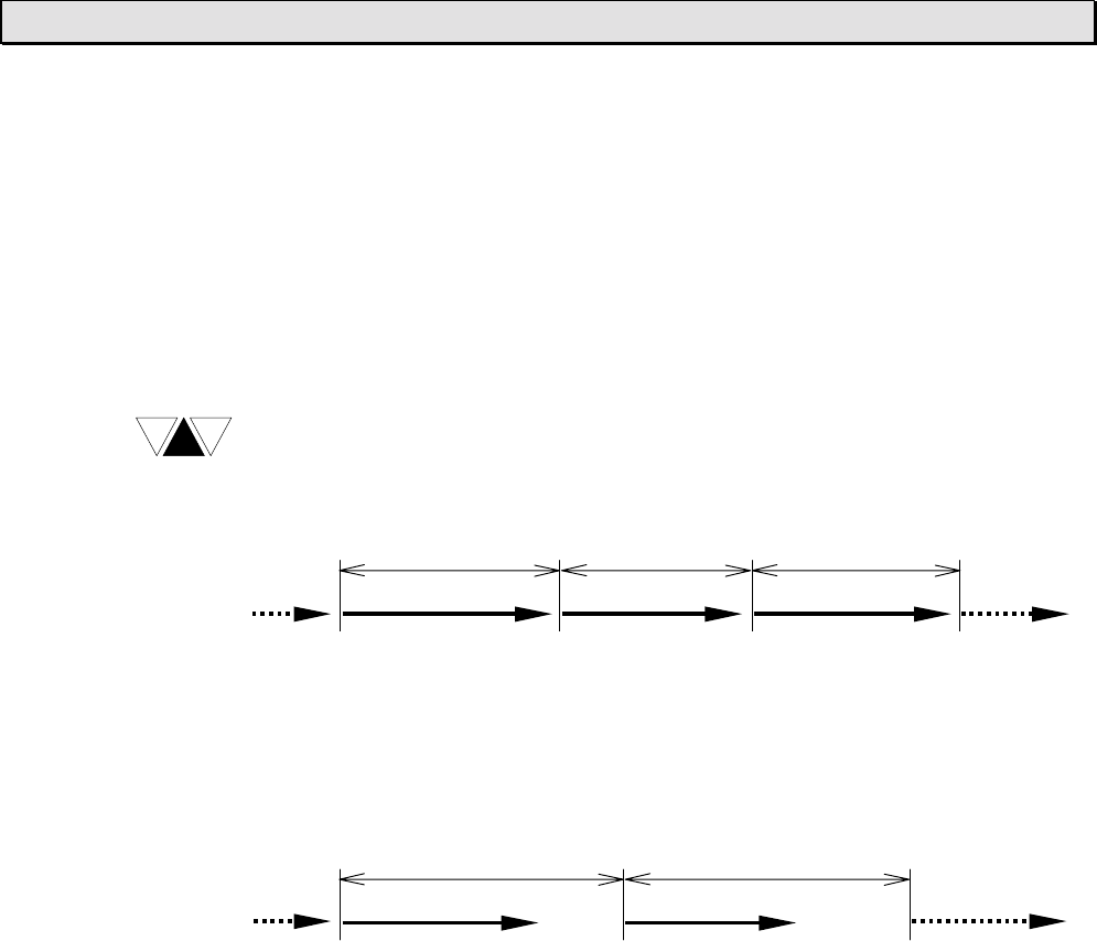
6F3B0253
Basic Hardware and Function 71
5. Operating System Overview
Self-diagnosis:
Checks the proper operation of the T1-16S itself. If an error has detected and cannot
be recovered by re-tries, the T1-16S moves into ERROR mode. For the self-diagnosis
items, refer to section 10.2.
Mode control:
Checks the mode control switch status and the mode control request commands from
the programming tool.
The scan mode − floating scan or fixed-time scan − is also controlled hear.
The floating scan:
When one scan is finished, immediately starts the next scan. The scan time
is shortest, but may vary depending on the program execution status.
Program check:
At the beginning of the RUN mode, the user program is compiled and its validity is
checked.
I/O update:
Reads the external input signals into the external input devices/registers (X/XW), and
sends the data of the external output devices/registers (Y/YW) to the external output
circuits. Then the outputs (relays, etc.) changes the states and latches until the next
I/O update timing.
The states of the forced input devices are not updated by this operation.
Timer update:
Updates the timer registers which are activated in the user program, and the timing
devices (S040 to S047).
The fixed-time scan:
The scan operation is started every user-specified time. The time setting
range is 10 to 200 ms (10 ms units). If an actual scan needs longer time
than the setting time, it works as the floating scan.
Scan timeScan time Scan time
Scan time (50 ms fixed) Scan time (50 ms fixed)
(idling) (idling)
NOTE

6F3B0253
72 T1-16S User’s Manual
5. Operating System Overview
User program execution:
Executes the programmed instructions from the beginning to the END instruction.
This is the essential function of the T1-16S.
In this section, only the main program execution is mentioned. For other program
types, such as timer interrupt, etc., refer to section 6.5.
Peripheral support:
Supports the communications with the programming tool or external devices
connected by the computer link function. The time for this operation is limited within
approx. 2 ms in the floating scan mode, and within allowable idling time in the fixed-
time scan mode.
If the special relay S158 is set to ON, the peripheral support priority mode is selected.
In the peripheral support priority mode, the peripheral support time is not limited. As
the result, the communication response is improved although the scan time becomes
long at the time.

6F3B0253
Basic Hardware and Function 73
Section 6
Programming Information
6.1 Devices and registers, 74
6.2 Index modification, 86
6.3 Real-time clock/calendar, 88
6.4 I/O allocation, 89
6.5 T1-16S memory mode setting, 91
6.6 User program configuration, 92
6.7 Programming language, 98
6.8 Program execution sequence, 99
6.9 On-line debug support functions, 100
6.10 Password protection, 103

6F3B0253
74 T1-16S User’s Manual
6. Programming Information
6.1 Devices and registers
The T1-16S program consists of bit-based instructions that handle ON/OFF
information, such as contact and coil instructions, and register-based (16-bit)
instructions, such as those for data transfer and arithmetic operations.
Devices are used to store the ON/OFF information of contacts and coils, and registers
are used to store 16-bit data.
Devices are divided into six types:
X External input devices
Y External output devices
R Auxiliary relay devices
S Special devices
T. Timer devices
C. Counter devices
Registers are divided into eight types:
XW External input registers
YW External output registers
RW Auxiliary relay registers
SW Special registers
T Timer registers
C Counter registers
D Data registers
I, J, K Index registers
Device and register numbers
X devices share the same memory area as XW registers. Device X004, for example,
represents the number 4 bit in the XW00 register.
Bit position / Number
(MSB) (LSB)
FEDCBA9876543210
XW00 1
X004
Thus, "X004 is ON" means that bit number 4 of XW00 is 1.
Y, R, and S devices work in a similar manner.

6F3B0253
Basic Hardware and Function 75
6. Programming Information
Addressing devices
A device number of X, Y, R and S devices consist of a register number and bit position
as follows.
X 00 4
Represents bit position 0 to F in the register.
Decimal number representing the register containing the corresponding
device.
Represents the type of device. (X, Y, R, or S)
As for the timer (T.) and the counter (C.) devices, a device number is expressed as
follows.
T. 12
Corresponding register number. (decimal number)
Represents the type of device. (T. or C.)
Dot (.) is used to identify as device.
Addressing registers
A register number except the index registers is expressed as follows.
XW 01
Register number. (decimal number)
Represents the type of register. (XW, YW, RW, SW, T, C or D)
The index registers (I, J and K) do not have the number.
J
I, J, or K
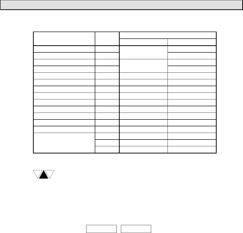
6F3B0253
76 T1-16S User’s Manual
6. Programming Information
Available address range
T1-16SDevice/register Symbol
Number of points Address range
External input device X X000 - X31F
External output device Y
Total 512 points
Y020 - Y31F
External input register XW XW00 - XW31
External output register YW
Total 32 words
YW02 - YW31
Auxiliary relay device R 4096 points R000 - R255F
Auxiliary relay register RW 256 words RW000 - RW255
Special device S 1024 points S000 - S63F
Special register SW 64 words SW00 - SW63
Timer device T. 256 points T.000 - T.255
Timer register T 256 words T000 - T255
Counter device C. 256 points C.000 - C.255
Counter register C 256 words C000 - C255
Data register D 4096 words D0000 - D4095
I 1 word I (no address)
J 1 word J (no address)
Index register
K 1 word K (no address)
(1) 1 word = 16 bits
(2) The available data range in each register is -32768 to 32767 (H8000 to
H7FFF) except for the timer and the counter registers.
The data range of the timer register is 0 to 32767. That of the counter
register is 0 to 65535.
(3) Double-word (32 bits) data is available in two consecutive registers.
In this case, lower address register stores the lower 16 bits data.
(MSB) F -------------0 F ------------ 0 (LSB)
Upper 16bits Lower 16bits
In this manual, a double-word register is expressed by using ‘⋅’.
For example, D0101⋅D0100.
D0100D0101
NOTE
6F3B0253
Basic Hardware and Function 77
6. Programming Information
External input devices (X)
These devices (X) indicate the ON/OFF states of external input signals through the
input circuits. External input devices can be used many times in a program.
External output devices (Y)
The external output devices (Y) store the ON/OFF signals that drive the external
devices through the output circuits. They can be used for coils in a program.
External input registers (XW)
These (XW) are 16-bit registers for storing values, which are received from the input
circuits.
External output registers (YW)
These 16-bit registers (YW) are used for storing values, which are sent to the output
circuits.
Auxiliary relay devices and registers (R/RW)
The auxiliary relay devices (R) are used to store intermediate results of sequences.
The auxiliary relay registers (RW) are used to store temporary results of function
instructions. The data in R/RW cannot be output directly to the output circuits. It is
necessary to move the data to Y/YW.
It is possible to make these registers retentive so that they retain data in the event of a
power failure. See section 5.3.
Timer devices and registers (T./T)
The timer registers (T) are used for storing the elapsed time of timer instructions, the
on-delay (TON), off-delay (TOF) and single-shot (SS) timers.
0.01 s base timers and 0.1 s base timers are provided.
Time base T1-16S
0.01 s T000 to T063
0.1 s T064 to T255
The timer devices (T.) work as the output of the timer instructions.
It is possible to specify the T registers as retentive to retain their data in the event of a
power failure. See section 5.3.

6F3B0253
78 T1-16S User’s Manual
6. Programming Information
Counter devices and registers (C./C)
The counter registers (C) are used for storing the count value of the counter (CNT)
and the up-down counter (U/D) instructions.
The counter devices (C.) work as the output of the counter instructions.
It is possible to specify the C registers as retentive to retain their data in the event of a
power failure. See section 5.3.
Data registers (D)
Functionally the data registers (D) are the same as auxiliary relay registers (RW)
except that the D registers cannot be used as devices.
A part of the data registers are saved in the built-in EEPROM as fixed data and
transferred into the RAM at the initial load.
The range of the data registers saved in the EEPROM can be specified by SW55.
See section 5.2.
It is possible to specify the D registers as retentive to retain their data in the event of a
power failure. See section 5.3.
Index registers (I, J, and K)
These index registers are used for indirect addressing for a register.
For example, if the value of I is 100 in the following register expression, it designates
D0100. For details, refer to section 6.2.
I
D0000 D0100 if I=100
6F3B0253
Basic Hardware and Function 79
6. Programming Information
Special devices and registers (S/SW)
The special devices (S) and special registers (SW) are used for special purposes. See
list below.
Device/
register Name Function
S000 0: Initialization 4: HOLD mode
S001 T1/T1S operation mode 1: HALT mode 6: ERROR mode
S002 2: RUN mode
S003 3: RUN-F mode
S004 CPU error (down) ON at error state (related to SW01)
S005 I/O error (down) ON at error state (related to SW02)
S006 Program error (down) ON at error state (related to SW03)
S007 EEPROM alarm (alarm) ON when EEPROM write exceeds 100,000 times
S008 Fixed-time scan time-over
(alarm) ON when actual scan time is longer than the setting
time as fixed-time scan
S009 −Reserved
S00A Clock/calendar error
(alarm) ON when clock/calendar data is illegal
S00B −Reserved
S00C −Reserved
S00D TL-F10 error (alarm) ON when TOSLINE-F10 transmission error occurs
S00E −Reserved
S00F Retentive data invalid
(alarm) ON when retentive data in RAM are invalid
(1) These devices are set by the T1-16S operating system. These devices
are read only for user.
(2) Devices marked as (down) are set in the ERROR mode. Therefore
these devices cannot be used in the user program.
(3) Devices marked as (alarm) are set in the normal operation mode.
These devices can be used in the user program.
NOTE

6F3B0253
80 T1-16S User’s Manual
6. Programming Information
Device/
register Name Function
S010 System ROM error (down) ON at error state
S011 System RAM error (down) ON at error state
S012 Program memory error
(down) ON at error state
S013 EEPROM error (down) ON at error state
S014 −Reserved
S015 −Reserved
S016 −Reserved
S017 −Reserved
S018 −Reserved
S019 −Reserved
S01A −Reserved
S01B −Reserved
S01C −Reserved
S01D −Reserved
S01E −Reserved
S01F Watchdog timer error
(down) ON at error state
S020 −Reserved
S021 I/O mismatch (down) ON at error state
S022 −Reserved
S023 −Reserved
S024 −Reserved
S025 −Reserved
S026 −Reserved
S027 −Reserved
S028 −Reserved
S029 −Reserved
S02A −Reserved
S02B −Reserved
S02C −Reserved
S02D −Reserved
S02E −Reserved
S02F −Reserved
(1) These devices are set by the T1-16S operating system. These devices
are read only for user.
(2) Devices marked as (down) are set in the ERROR mode. Therefore
these devices cannot be used in the user program.
NOTE
6F3B0253
Basic Hardware and Function 81
6. Programming Information
Device/
register Name Function
S030 Program error ON at error state (related to SW06)
S031 Scan time over (down) ON when the scan time exceeds 200 ms
S032 −Reserved
S033 −Reserved
S034 −Reserved
S035 −Reserved
S036 −Reserved
S037 −Reserved
S038 −Reserved
S039 −Reserved
S03A −Reserved
S03B −Reserved
S03C −Reserved
S03D −Reserved
S03E −Reserved
S03F −Reserved
S040 Timing relay 0.1 s OFF 0.05 s / ON 0.05 s (0.1 s interval)
S041 Timing relay 0.2 s OFF 0.1 s / ON 0.1 s (0.2 s interval)
S042 Timing relay 0.4 s OFF 0.2 s / ON 0.2 s (0.4 s interval) All OFF at the
S043 Timing relay 0.8 s OFF 0.4 s / ON 0.4 s (0.8 s interval) beginning of
S044 Timing relay 1.0 s OFF 0.5 s / ON 0.5 s (1.0 s interval) RUN mode
S045 Timing relay 2.0 s OFF 1.0 s / ON 1.0 s (2.0 s interval)
S046 Timing relay 4.0 s OFF 2.0 s / ON 2.0 s (4.0 s interval)
S047 Timing relay 8.0 s OFF 4.0 s / ON 4.0 s (8.0 s interval)
S048 −Reserved
S049 −Reserved
S04A −Reserved
S04B −Reserved
S04C −Reserved
S04D −Reserved
S04E Always OFF Always OFF
S04F Always ON Always ON
(1) These devices are set by the T1-16S operating system. These devices
are read only for user.
(2) Devices marked as (down) are set in the ERROR mode. Therefore
these devices cannot be used in the user program.
NOTE

6F3B0253
82 T1-16S User’s Manual
6. Programming Information
Device/
register Name Function
S050 CF (carry flag) Used for instructions which manipulate carry
S051 ERF (instruction error flag) ON when instruction execution error is occurred
(related to alarm flags of SW06)
S052 −Reserved
S053 −Reserved
S054 −Reserved
S055 −Reserved
S056 −Reserved
S057 −Reserved
S058 −Reserved
S059 −Reserved
S05A −Reserved
S05B −Reserved
S05C −Reserved
S05D −Reserved
S05E −Reserved
S05F −Reserved
S060 Illegal instruction (down) ON when illegal instruction is detected
S061 −Reserved
S062 −Reserved
S063 −Reserved
S064 Boundary error (alarm) ON when illegal address is designated by indirect
addressing (operation continued)
S065 −Reserved
S066 −Reserved
S067 −Reserved
S068 Division error (alarm) ON when error occurs in division instruction (operation
continued)
S069 BCD data error (alarm) ON when BCD data error has detected in BCD
operation instructions (operation continued)
S06A Table operation error
(alarm) ON when table size error has detected in table
operation instructions (operation continued) (T1S only)
S06B Encode error (alarm) ON when error occurs in encode instruction (operation
continued)
S06C −Reserved
S06D −Reserved
S06E −Reserved
S06F −Reserved
NOTE (1) Devices marked as (down) are set in the ERROR mode. Therefore
these devices cannot be used in the user program.
(2) CF, ERF and devices marked as (alarm) can be reset by the user
program.

6F3B0253
Basic Hardware and Function 83
6. Programming Information
Device/
register Name Function
SW07 Clock/calendar (Year) Lower 2 digits of the calendar year
(01, 02, ... )
SW08 Clock/calendar (Month) Month (01, 02, ... 12) They are stored in
SW09 Clock/calendar (Day) Day (01, 02, ... 31) the lower 8 bits by
SW10 Clock/calendar (Hour) Hour (00, 01, ... 59) BCD code
SW11 Clock/calendar (Minute) Minute (00, 01, ... 59)
SW12 Clock/calendar (Second) Second (00, 01, ... 59)
SW13 Clock/calendar (Week) Day of the week
(Sun = 00, Mon = 01, ... Sat = 06)
SW14 −Reserved
SW15 Peripheral support priority Bit 8 (S158) is used to select peripheral support priority
SW16 Mode of special input
functions Used to select the special input functions
SW17 Input filter constant Used to set the input filter constant
SW18 Preset values for high Used to set the preset values for high speed counters
SW19 speed counter
SW20
SW21
SW22 Count values for high Present count values of the high speed counters are
SW23 speed counter stored
SW24 High speed counter control
flags Control flags for the high speed counters
SW25 −Reserved
SW26 Mode of special output
functions Used to select the special output functions
SW27 Special output control flags Control flags for the pulse/PWM output
SW28 Special output frequency
setting Output frequency setting for the pulse/PWM output
SW29 PWM output duty setting Pulse duty setting for the PWM output
SW30 Analog setting value 1 Input value of the analog setting adjuster V0
SW31 Analog setting value 2 Input value of the analog setting adjuster V1
SW32 −Reserved
SW33 −Reserved
SW34 TL-F10 send data TOSLINE-F10 transmission data (send to master)
SW35 TL-F10 receive data TOSLINE-F10 transmission data (receive from master)
SW36 PRG port station address Used to set the programmer port station address
(1 to 32)
SW37 PRG port parity Used to set the programmer port parity (0=none,
1=odd)
SW38 PRG port response delay Used to set the programmer port response delay time
(0 to 30: 0 to 300ms)
(1) These devices are set by the T1-16S operating system. These devices
are read only for user.
(2) Devices marked as (down) are set in the ERROR mode. Therefore
these devices cannot be used in the user program.
NOTE

6F3B0253
84 T1-16S User’s Manual
6. Programming Information
Device/
register Name Function
S390 Timer interrupt execution
status ON during execution
S391 I/O interrupt #1 execution
status ON during execution
S392 I/O interrupt #2 execution
status ON during execution
S393 I/O interrupt #3 execution
status ON during execution
S394 I/O interrupt #4 execution
status ON during execution
S395 −Reserved
S396 −Reserved
S397 −Reserved
S398 −Reserved
S399 −Reserved
S39A −Reserved
S39B −Reserved
S39C −Reserved
S39D −Reserved
S39E −Reserved
S39F −Reserved
S400 −Reserved
S401 HOLD device ON during HOLD mode (setting by user program is also
available)
S402 −Reserved
S403 −Reserved
S404 −Reserved
S405 −Reserved
S406 −Reserved
S407 −Reserved
S408 −Reserved
S409 −Reserved
S40A −Reserved
S40B −Reserved
S40C −Reserved
S40D −Reserved
S40E −Reserved
S40F −Reserved
6F3B0253
Basic Hardware and Function 85
6. Programming Information
Device/
register Name Function
SW41 Sub-program #1 execution
status Bit 0 (S410) is ON during the sub-program #1 is
executed
SW42 −Reserved
SW43 −Reserved
SW44 −Reserved
SW45 −Reserved
SW46 −Reserved
SW47 −Reserved
SW48 −Reserved
SW49 −Reserved
SW50 −Reserved
SW51 −Reserved
SW52 −Reserved
SW53 −Reserved
SW54 Basic unit I/O LED display
mode Used to display the selected I/O module status
(0 = Basic unit, 1 to 8 = I/O module slot 0 to 7,
9 and 10 = TOSLINE-F10)
SW55 Number of EEPROM write
data Used to set the number of data registers to be saved in
the EEPROM (0 to 2048, initial value is 2048)
SW56 RS-485 port operation
mode Used to set the RS-485 port operation mode
(0 = Computer link, 1 = Data link, 2 = Free ASCII,
3 = Inverter connection)
SW57 RS-485 port response
delay Used to set the RS-485 port response delay time
(0 to 30: 0 to 300ms)
SW58 RS-485 port Free ASCII
flags Used for the RS-485 port Free ASCII function
SW59 −Reserved
SW60 −Reserved
SW61 −Reserved
SW62 −Reserved
SW63 −Reserved
(1) For details of SW54, refer to section 1.5.1.
(2) For details of SW55, refer to section 5.2.
(3) For details of SW56 through SW58, refer to the Communication
function manual.
NOTE

6F3B0253
86 T1-16S User’s Manual
6. Programming Information
6.2 Index modification
When registers are used as operands of instructions, the method of directly
designating the register address as shown in Example 1) below is called ‘direct
addressing’.
As opposed to this, the method of indirectly designating the register by combination
with the contents of the index register (I, J, or K) as shown in Example 2) below is
called ‘indirect addressing’. In particular, in this case, since the address is modified
using an index register, this is called ‘index modification’.
Example 1)
[ RW10 MOV D1000 ]
Data transfer instruction
Transfer data of RW10 to D1000
Example 2)
I J
[ RW10 MOV D0000 ]
Data transfer instruction (with index modification)
Transfer data of RW(10 + I) to D(0000 + J)
(If I = 3 and J = 200, the data of RW13 is transferred to D0200)
There are 3 types of index register, I, J and K. Each type processes 16-bit integers
(-32768 to 32767). There are no particular differences in function between these 3
types of index register.
There is no special instruction for substituting values in these index registers. These
are designated as destination of data transfer instructions, etc.
[ 00064 MOV I ](substitutes 64 in index register I)
[ D0035 MOV J ](substitutes the data of D0035 in index register J)
[ RW20 + 00030 → K ](substitutes the result of addition in index register K)
(1) The index modification is available for RW, T, C and D registers.
(2) If index registers are used as a double-length register, only the
combinations J×I and K×J are allowed.
NOTE
6F3B0253
Basic Hardware and Function 87
6. Programming Information
The followings are examples of index modifications.
When I = 0, it designates RW10.
When I = 1, it designates RW11.
When I = -1, it designates RW09.
When I = 10, it designates RW20.
When I = -10, it designates RW00.
When J = 0, it designates D0201⋅D0200.
When J = 1, it designates D0202⋅D0201.
When J = 2, it designates D0203⋅D0202.
When J = -1, it designates D0200⋅D0199.
When J = -2, it designates D0199⋅D0198.
Be careful that the registers do not exceed the address range by the index
modification. The address range is not checked by the T1-16S.
Substitutions of values into index registers and index modifications can be
used any times in a program. Normally, the program will be easier to see if
a value substitution into an index register is positioned immediately before
the index modification.
!CAUTION
I
RW10
J
D0201
⋅
D0200
NOTE
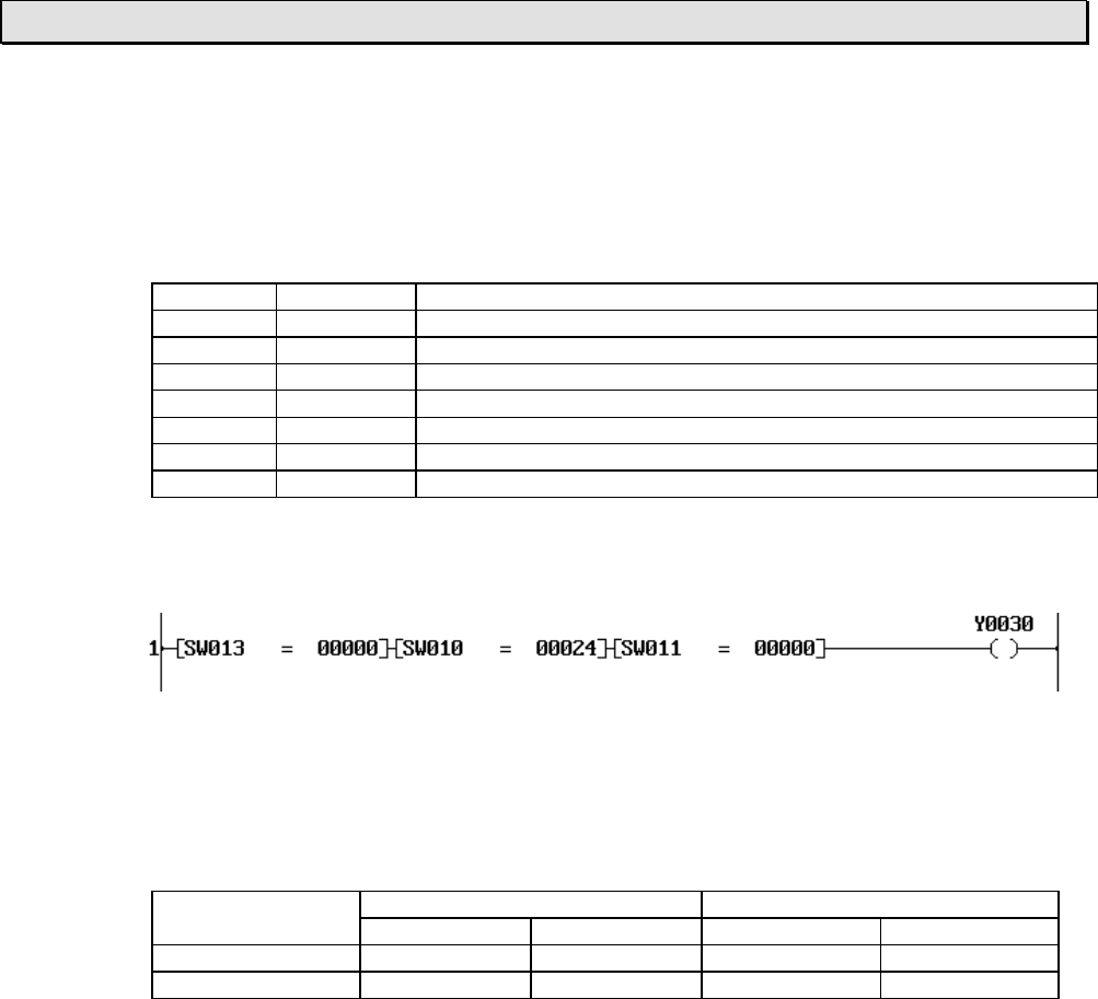
6F3B0253
88 T1-16S User’s Manual
6. Programming Information
6.3 Real-time clock/calendar (Enhanced model only)
The T1-16S enhanced model is equipped with the real-time clock/calendar for year,
month, day, day of the week, hour, minute, and second.
These data are stored in the special registers SW07 to SW13 by 2-digit BCD format
as follows.
Register Function Data
SW07 Year 1999 = H0099, 2000 = H0000, 2001 = H0001, 2002 = H0002 ...
SW08 Month Jan. = H0001, Feb. = H0002, Mar. = H0003, ... Dec. = H0012
SW09 Day 1st = H0001, 2nd = H0002, 3rd = H0003, ... 31st = H0031
SW10 Hour H0000, H0001, H0002, ... H0022, H0023
SW11 Minute H0000, H0001, H0002, ... H0058, H0059
SW12 Second H0000, H0001, H0002, ... H0058, H0059
SW13 Week Sun. = H0000, Mon. = H0001, Tue. = H0002, ... Sat. = H0006
Program example:
In the following circuit, output Y030 turns ON for 1 minute at every Sunday 6 pm.
Clock/calendar back up:
The clock/calendar continues updating even while the power to the T1-16S is off by
built-in capacitor and by the optional battery (CR2032) if used. Its buck-up period is as
follows.
Expected value Guarantee value
Environment
temperature Capacitor Battery Capacitor Battery
Under 30 °C (86 °F) 2 hours 2 year 1 hours 1 year
Over 30 °C (86 °F) 1 hours 1 year 30 minutes 6 months
As shown in the table, it is recommended to use the optional battery when the real-
time clock/calendar function is used.
In the T1-16S, the validity of the clock/calendar is checked. If the data is not valid by
excess power off period, special relay S00A is set to ON. Therefore, when the
clock/calendar is used, it is recommended to check the status of S00A in the user
program.
Setting the clock/calendar:
To set the clock/calendar data, the following 2 ways are available. In both cases, the
week data is automatically calculated.
(1) Setting the clock/calendar data on the system information screen of the
programming tool.
(2) Using the Calendar Set instruction (CLND) in the user program.
(H0018)

6F3B0253
Basic Hardware and Function 89
6. Programming Information
6.4 I/O allocation
The external input signals are allocated to the external input devices/registers (X/XW).
The external output signals are allocated to the external output devices/registers
(Y/YW).
The register numbers of the external input and output registers are consecutive. Thus
one register number can be assigned for either input or output.
As for the T1-16S basic unit, I/O allocation is fixed as follows.
Inputs: 8 points (X000 - X007)
T1-16S Outputs: 8 points (Y020 - Y027)
X000 --- X007 Y020---- Y027
Any operations for the I/O allocation are not required if only the T1-16S basic unit is
used.
However, if the I/O modules are used with the T1-16S, the I/O allocation operation is
necessary. Refer to the separate manual "T1-16S User's Manual - I/O Modules -".
6F3B0253
90 T1-16S User’s Manual
6. Programming Information
Internally, the T1-16S has information called ‘I/O allocation table’ in its memory. This
I/O allocation table shows the correspondence between I/O hardware and software,
i.e. register/device.
The contents of the I/O allocation table are as follows.
Unit Slot I/O type
PU
0 X+Y 4W
1
2
3
4
5
6
0
7
0
1
2
3
4
5
6
1
7
The T1-16S operating system automatically sets the I/O type ‘X+Y 4W’ on the slot 0 at
unit 0 position when the memory clear is executed for the T1-16S.
When the T1-16S program is developed in off-line, the above I/O allocation table
should be set before programming. For this operation (called manual I/O allocation),
refer to the programming tool manual.
(1) Unit base address setting function is not supported by the T1-16S.
Do not use this function with the T1-16S. It will causes malfunction.
(2) When the TOSLINE-F10 station module FR112M is used, allocate it at
the end of the I/O modules.
NOTE
PU slot must be blank
Slot 0 is for basic unit (XW00, XW01, YW02
and YW03 are assigned internally)
Slots 1 to 7 of unit 0 are not used
(must be blank)
These slots are for I/O modules

6F3B0253
Basic Hardware and Function 91
6. Programming Information
6.5 T1-16S memory mode setting
The program capacity of the T1-16S is 8 k steps. However, user can set the T1-16S’s
program capacity to 4 k steps. It is called the T1-16S’s memory mode.
That is, the T1-16S has two memory modes, 8 k mode and 4 k mode.
In the 4 k mode, on-line program changes become available, although the program
capacity is limited to 4 k steps. Refer to section 6.9 for the on-line debug support
functions.
To set the T1-16S’s memory mode, write 4 k or 8 k on the Program Size Setting of the
System Parameters using the programming tool. Then execute the EEPROM write
command.

6F3B0253
92 T1-16S User’s Manual
6. Programming Information
6.6 User program configuration
A group of instructions for achieving the PLC-based control system is called ‘user
program’. The T1-16S has 8 k steps capacity for storing the user program.
A ‘step’ is the minimum unit, which composes an instruction. Number of steps required
for one instruction is depending on the type of instruction. Refer to section 7.1.
The figure below shows the T1-16S’s memory configuration.
RAM
For conditions of transfer between RAM and EEPROM, see section 5.2.
System information
Back-up area
by EEPROM
4 k or 8 k steps User program
Data registers
mentioned in
section 5.2
Other registers/
devices
NOTE

6F3B0253
Basic Hardware and Function 93
6. Programming Information
System information
System information is the area which stores execution control parameters. The
following contents are included in the system information.
(1) Machine parameters (hardware type, memory type)
(2) User program information (program ID, system comments, number of steps used)
(3) Passwords
(4) Retentive register area information
(5) T1S program memory mode, 4 k steps or 8 k steps
(6) Execution control parameters (scan mode, timer interrupt interval)
(7) Station number setting for programmer port (T1), or RS-485 port communication
parameters (Enhanced model)
(8) I/O allocation table
(9) Input force table
The system information is stored in the built-in EEPROM. Therefore, when this
information is modified, the EEPROM write operation is necessary. Otherwise, these
are over-written by original EEPROM contents at the next initial load timing.
User program
The T1-16S has a capacity of 8 k steps of the user program.
The user program is stored by each program types as shown in the following diagram,
and is managed by units called blocks in each program types.
User program configuration Program type internal configuration
(Program types) (Blocks)
Subroutine
I/O interrupt #4
I/O interrupt #3
I/O interrupt #2
I/O interrupt #1
Timer interrupt
Sub-program #1
Block 1
Block N
(N = max. 256)
Block 10
Block 2
Block 1
Main program
6F3B0253
94 T1-16S User’s Manual
6. Programming Information
In the user program, the main program is the core. The scan operation explained in
section 5.3 is for the main program. The operation of other program types are
explained in the following sections.
The following 8 program types are supported by the T1-16S.
(1) Main program
(2) Sub-program #1
(3) Timer interrupt program
(4) I/O interrupt program #1
(5) I/O interrupt program #2
(6) I/O interrupt program #3
(7) I/O interrupt program #4
(8) Subroutine
The blocks are just separators of the program, and have no effect on the program
execution. However, by dividing the user program into some blocks, the program
becomes easy to understand. The block numbers need not be consecutive.
In each program type and block, there is no limit of program capacity. The only limit is
the total capacity.
6.6.1 Main program
The main program is the core of the user program. It is executed once in each scan.
In the above figure,
Mode means the mode control operation
I/O means the I/O update processing
Timer means the timer up date processing
Main program means the main program execution
the self-diagnostic check and peripheral support are omitted in this figure.
The end of the main program is recognized by the END instruction.
Although instructions may be present after the END instruction, these portions will not
be executed.
Mode Main programTimerI/O I/OMode
1 scan time
Time
Main program
Timer
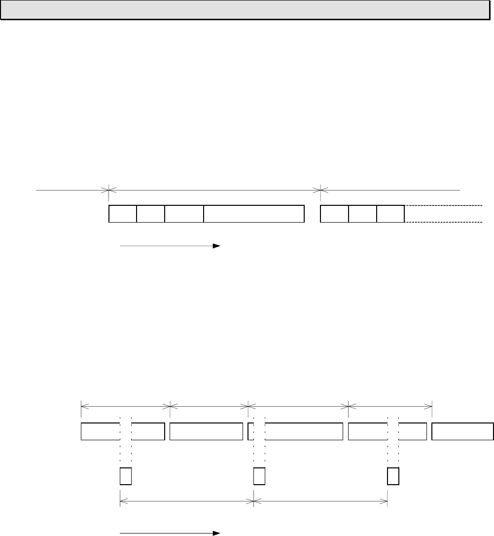
6F3B0253
Basic Hardware and Function 95
6. Programming Information
6.6.2 Sub-program #1
If the sub-program #1 is programmed, it is executed once at the beginning of the first
scan (before main program execution).
Therefore, the sub-program #1 can be used to set the initial value into the registers.
The sub-program #1 is called the initial program.
The figure below shows the first scan operation.
The end of the sub-program #1 is recognized by the END instruction.
6.6.3 Timer interrupt program
The timer interrupt is the highest priority task. It is executed cyclically with a user
specified interval, with suspending other operation.
The interrupt interval is set in the system information. (5 to 1000 ms, 5 ms units)
The end of the timer interrupt is recognized by the IRET instruction.
I/O Main program
Main programSub#1Timer I/OMode Timer
RUN mode
transition 1st scan 2nd scan
Time
1 scan1 scan1 scan
Scan
Timer interrupt
1 scan
Timer interrupt
interval
Timer interrupt
interval
Time

6F3B0253
96 T1-16S User’s Manual
6. Programming Information
6.6.4 I/O interrupt programs
The I/O interrupt program is also the highest priority task. It is executed immediately
when the interrupt factor is generated, with suspending other operation.
The following 4 types I/O interrupt programs are supported in the T1/T1S.
(1) I/O interrupt #1
The I/O interrupt #1 is used with the high speed counter function. When the count
value reaches the preset value, etc., the I/O interrupt #1 is activated immediately
with suspending other operation. The end of the I/O interrupt #1 is recognized by
the IRET instruction. For detailed information, refer to section 8.3.
(2) I/O interrupt #2
The I/O interrupt #2 is also used with the high speed counter function. Refer to
section 8.3 for details.
(3) I/O interrupt #3
The I/O interrupt #3 is used with the interrupt input function. When the state of the
interrupt input is changed from OFF to ON (or ON to OFF), the I/O interrupt #3 is
activated immediately with suspending other operation. The end of the I/O
interrupt #3 is also recognized by the IRET instruction. For detailed information,
refer to section 8.4.
(4) I/O interrupt #4
The I/O interrupt #4 is also used with the interrupt input function. Refer to section
8.4 for details.
If an interrupt factor is generated while other interrupt program is executing (including
the timer interrupt), the interrupt factor is held. Then it will be activated after finishing
the other interrupt program execution.
If two or more interrupt factors are generated at the same time, the priority is as
follows.
Timer > I/O #1 > I/O #2 > I/O #3 > I/O #4
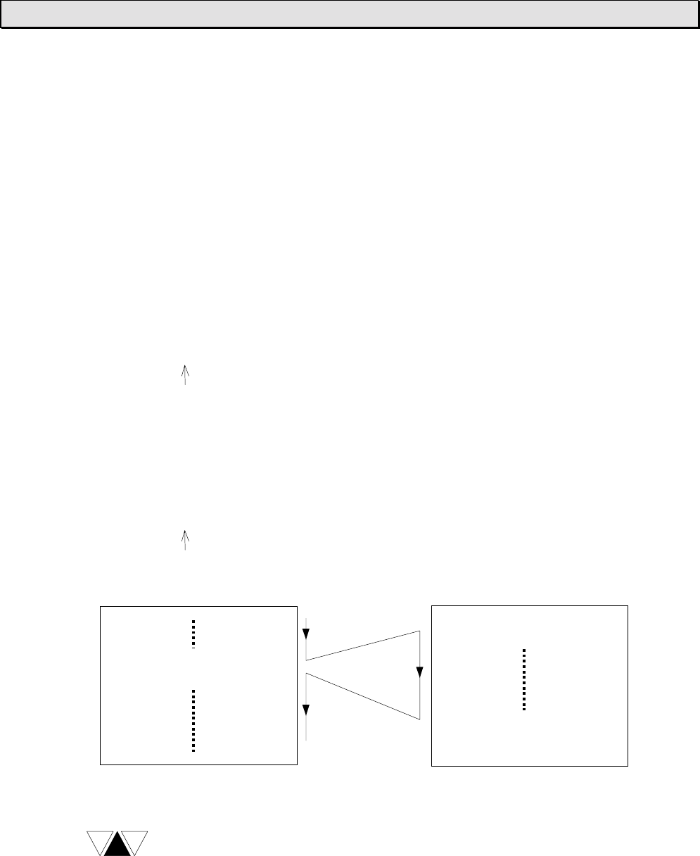
6F3B0253
Basic Hardware and Function 97
6. Programming Information
6.6.5 Subroutines
In the program type ‘Subroutine’, The following number of subroutines can be
programmed.
The T1-16S supports up to 256 subroutines.
The subroutine is not a independent program. It is called from other program types
(main program, sub-program, interrupt program) and from other subroutines.
One subroutine is started with the SUBR instruction, and ended by the RET
instruction.
It is necessary to assign a subroutine number to the SUBR instruction. The available
subroutine numbers are 0 to 255.
[ SUBR (000) ]
Subroutine number
The RET instruction has no subroutine number.
The instruction that calls a registered subroutine is the CALL instruction. The CALL
instruction has the subroutine number to be called.
[ CALL N.000 ]
Subroutine number
Main program Subroutine
[ SUBR (000) ]
[ CALL N.000 ]
[ RET ]
(1) Multiple subroutines can be programmed in a block. However, one
subroutine in one block is recommended.
(2) From the inside of a subroutine, other subroutines can be called
(nesting). Its allowable level is up to 3 levels.
NOTE
Execution
flow
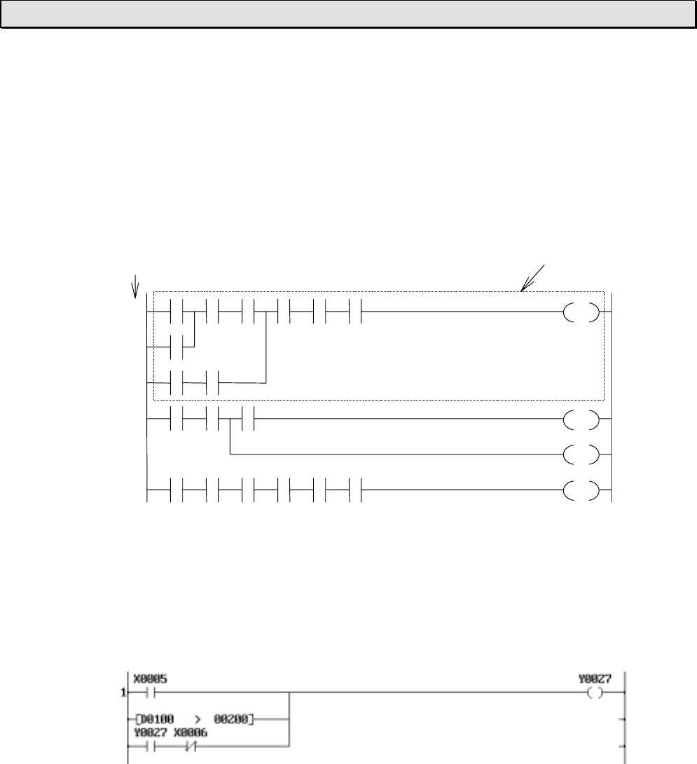
6F3B0253
98 T1-16S User’s Manual
6. Programming Information
6.7 Programming language
The programming language of the T1-16S is ‘ladder diagram’.
Ladder diagram is a language, which composes program using relay symbols as a
base in an image similar to a hard-wired relay sequence. In the T1/T1S, in order to
achieve an efficient data-processing program, ladder diagram which are combinations
of relay symbols and function blocks are used.
The ladder diagram program is constructed by units called ‘rung’. A rung is defined as
one network which is connected each other.
The rung numbers are a series of numbers (decimal number) starting from 1, and
cannot be skipped. There is no limit to the number of rungs.
The size of any one rung is limited to 11 lines × 12 columns.
A example of a ladder diagram program is shown below.
When X005 is ON or the data of D0100 is greater than 200, Y027 comes ON.
Y027 stays ON even if X005 is OFF and the data of D0100 is 200 or less.
Y027 will come OFF when X006 comes ON.
RungRung number
1
2
3
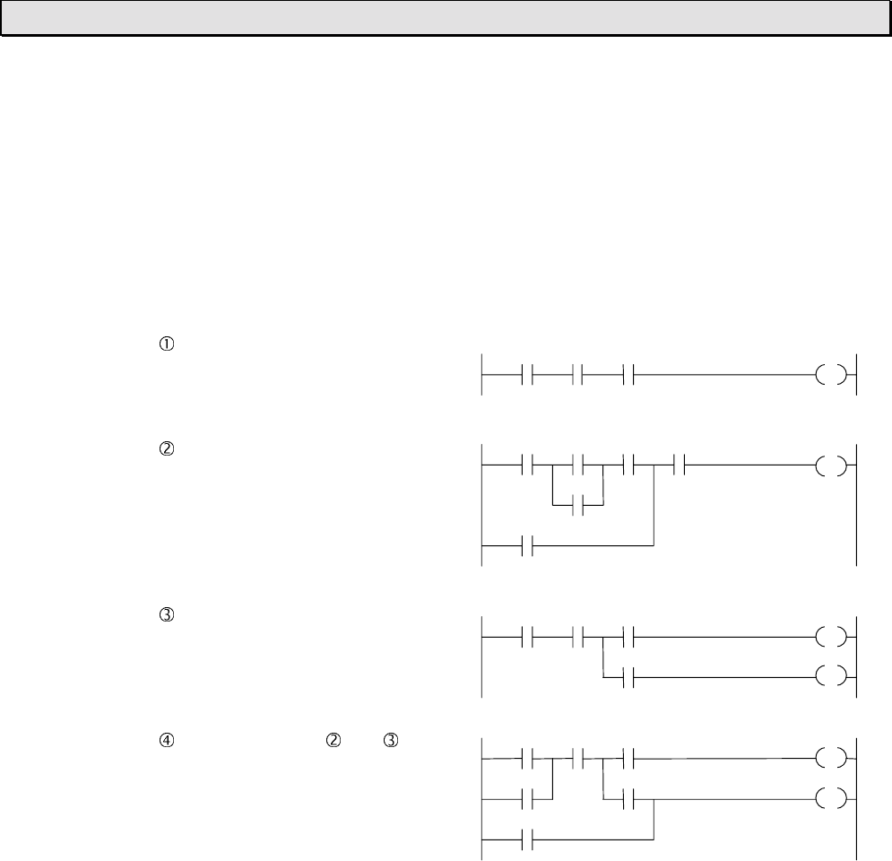
6F3B0253
Basic Hardware and Function 99
6. Programming Information
6.8 Program execution sequence
The instructions execution sequence is shown below.
(1) They are executed in the sequence from block 1 through the final block, which
contains the END instruction (or IRET in an interrupt program).
(2) They are executed in the sequence from rung 1 through the final rung in a block
(or the END instruction).
(3) They are executed according to the following rules in any one rung.
When there is no vertical
connection, they are
executed from left to right.
When there is an OR
connection, the OR logic
portion is executed first.
When there is a branch, they
are executed in the order from
the upper line to the lower line.
A combination of and
above.
The instructions execution sequence in which function instructions are included also
follows the above rules. However, for program execution control instructions, such as
jumps (JCS), loops (FOR-NEXT), subroutines (CALL-SUBR-RET), it will depend the
specifications of each instruction.
4321
86
7
2
5431
6
4
5
321
5
3
76421
6F3B0253
100 T1-16S User’s Manual
6. Programming Information
6.9 On-line debug support functions
The following on-line (during RUN) functions are supported in the T1-16S for effective
program debugging.
On-line function 4 k mode 8 k mode
Force function Yes Yes
Sampling trace function Yes Yes
Changing timer /counter
preset value Yes Yes
Changing constant operand of
function instruction Yes Yes
Changing device directly Yes Yes
Program changing in edit
mode Yes No
EEPROM write command Yes Yes
Refer to section 6.5 for 4 k/8 k mode.
Force function
Two types of force functions are available, input force and coil force.
The input force is used to disable the external input signals. When an external input
device is designated as forced input, the ON/OFF state of the device can be changed
manually by using the data setting function of the programming tool, regardless of the
corresponding external signal state. The input force designation is available for the
external input devices (X).
The coil force is used to disable the coil instruction. When a coil instruction on the
program is designated as forced coil, the ON/OFF state of the coil device can be
changed manually by using the data setting function of the programming tool,
regardless of the coil circuit execution status.
On the programming tool, the forced input and forced coil are expressed as follows.
Forced input
ForcedNormal
X005 x005
Forced coil
ForcedNormal
Y023 Y023
If EEPROM write operation is executed with remaining the force
designation, the force designation is also saved into the built-in EEPROM.
Because the force function is debugging function, release all force
designation before executing the EEPROM write operation. The force batch
release command is available when the T1-16S is in HALT mode.
NOTE
NOTE
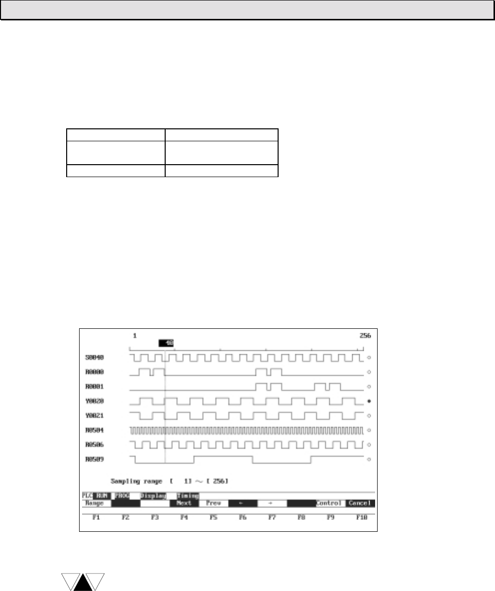
6F3B0253
Basic Hardware and Function 101
6. Programming Information
Sampling trace function
The sampling trace function collects the status of specified devices or register at every
specified sampling timing. The collected data can be displayed on the programmer
(T-PDS) screen in the format of timing chart (for devices) or trend graph (for register).
The minimum sampling timing is the T1-16S’s scan cycle.
This function is useful for program debugging and troubleshooting.
T1-16S
Sampling target Devices (up to 8) and
Registers (up to 3)
Sampling capacity 256 times
The collected data is stored in the T1-16S internal buffer.
The buffer works as a ring buffer, and latest collected data can be displayed.
The sampling start/stop condition (arm condition) and the collection timing (trigger
condition) can be specified by status changing of devices.
For detailed key operations for arm/trigger conditions setting on the T-PDS, refer to
the manual for T-PDS.
T-PDS screen example of device timing chart
(1) On the T-PDS, select ‘3 registers + 8 devices’ as the sampling type.
(2) As the arm and trigger conditions, register values cannot be used.
(3) The After times setting is not effective for the T1-16S.
NOTE

6F3B0253
102 T1-16S User’s Manual
6. Programming Information
Timer/counter preset value (constant data) changing
The preset value (constant data) of timer or counter instruction can be changed in on-
line (during RUN) by using the programming tool.
Function instruction constant operand changing
The constant operand of function instruction can be changed in on-line (during RUN)
by using the programming tool.
Device changing
The device of contact or coil instruction can be changed in on-line (during RUN) by
using the programming tool.
On-line program changing
When the T1S’s memory mode is 4 k mode, the program can be changed using
normal edit mode. (rung by rung)
In the on-line program changing, it is not allowed to change the number or order of the
following instructions.
END, MCS, MCR, JCS, JCR, FOR, NEXT, CALL, SUBR, RET, IRET
The above on-line functions are performed on the RAM memory. Therefore,
when program has been changed, execute the EEPROM write operation
before turning off power. Otherwise, program stored in the EEPROM will be
overwritten.
On-line EEPROM write
The EEPROM write is possible in on-line (during RUN) as well as in HALT mode.
In the on-line EEPROM write, user data is not written into the EEPROM.
During this operation, the T1-16S’s scan time becomes longer. However, as it has the
time limit per scan, the T1-16S’s control operation is not stopped.
NOTE

6F3B0253
Basic Hardware and Function 103
6. Programming Information
6.10 Password protection
The T1-16S has the password function to protect the user program and data from
unauthorized operations.
There are four levels of protection. Accordingly, three levels of passwords can be
registered to control the protection levels.
These passwords are stored in the built-in EEPROM. Therefore, if you entered,
changed or cleared the passwords, the EEPROM write operation is necessary.
The outline of the protection levels are shown below. For details, refer to the manual
for the programming tool.
Protection level 4 (disabled functions)
• Writing register/device data
• Writing system information
• I/O allocation
Protection level 3 (disabled functions)
• Reading program
• Program write into EEPROM
Protection level 2 (disabled functions)
• Clear memory
• Writing/loading program
• T1/T1S operation mode changes (by programming tool)
• Setting/changing passwords
Protection level 1 (disabled functions)
• None (all functions are available)
When the level 1, 2 and 3 passwords are registered, the T1-16S will be started as
protection level 4. In this state, for example, entering the level 2 password changes
the protection level to 2.
When you use the password function, do not forget the level 1 password.
Otherwise, you cannot change/release the registered passwords.
Strict
NOTE
6F3B0253
104 T1-16S User’s Manual

6F3B0253
Basic Hardware and Function 105
Section 7
Instructions
7.1 List of instructions, 106
7.2 Instruction specifications, 116
6F3B0253
106 T1-16S User’s Manual
7. Instructions
7.1 List of instructions
The T1-16S has 21 types of basic ladder instructions and 97 types of function
instructions as listed below. The specifications of each instruction will be described in
detail later.
The tables listing these instructions are provided as a quick reference. (Note: In the
following table, italic character means operand, i.e. register, device or constant value.)
Basic ladder instructions
FUN
No. Name Expression Function Steps Speed
(µs) Page
−NO contact ANO (normally open) contact of
device A. 1 1.4 - 3.3 117
−NC contact A
NC (normally closed) contact
of device A. 1 1.4 - 3.3 118
−Transitional
contact (rising) Turns ON output for 1 scan
when input changes from OFF
to ON. 1 3.0 119
−Transitional
contact (falling) Turns ON output for 1 scan
when input changes from ON
to OFF. 1 3.0 120
−Coil A
Relay coil of device A. 1 2.3 121
−Forced coil A
Forced coil of device A. State
of device A is retained
regardless of the input state. 1 2.3 122
−Inverter I Inverts the input state. 1 1.4 - 3.3 123
−Invert coil A
I Stores the inverse state of
input into device A. 1 2.3 124
−Positive pulse
contact A
P Turns ON output for 1 scan
when input is ON and device A
changes from OFF to ON. 1 125
−Negative pulse
contact A
N Turns ON output for 1 scan
when input is ON and device A
changes from ON to OFF. 1 126
−Positive pulse coil A
P Turns ON device A for 1 scan
when input changes from OFF
to ON. 1 127
−Negative pulse coil A
N Turns ON device A for 1 scan
when input changes from ON
to OFF. 1 128
−ON delay timer −[ A TON B ]−Turns ON output when the
time specified by A has
elapsed after the input came
ON. B is a timer register.
2 12.6 129
−OFF delay timer −[ A TOF B ]−Turns OFF output when the
time specified by A has
elapsed after the input came
OFF. B is a timer register.
2 12.8 130
−Single shot timer −[ A SS B ]−Turns ON output for the time
specified by A when the input
comes ON. B is a timer
register.
2 13.0 131

6F3B0253
Basic Hardware and Function 107
7. Instructions
Basic ladder instructions (continued)
FUN
No. Name Expression Function Steps Speed
(µs) Page
−Counter C CNT Q
E A B Counts the number of cycles
the count input (C) comes ON
while the enable input (E) is
ON, and turns ON output (Q)
when the count reaches to the
value specified by A. B is a
counter register.
2 22.6 132
−Master control set −−[ MCS ]− 1
−Master control reset −−[ MCR ]−
Turns OFF power rail between
MCS and MCR when MCS
input is OFF. 1
3.75
(in a
pair) 133
−Jump control set −−[ JCS ]− 1
−Jump control reset −−[ JCR ]−
Jumps from JCS to JCR when
JCS input is ON. 1
2.75
(in a
pair) 134
−End −−[ END ]− Indicates end of main program
or sub-program. 1 1.4 135
Data transfer instructions
FUN
No. Name Expression Function Steps Speed
(µs) Page
018 Data transfer −[ A MOV B ]−Transfers data of A to B. 3 4.2 136
019 Double-word
data transfer
−[ A+1⋅A DMOV B+1⋅B ]−Transfers double-word data
of A+1⋅A to B+1⋅B. 3 7.2 137
020 Invert transfer −[ A NOT B ]−Transfers bit-inverted data of
A to B. 3 4.6 138
022 Data exchange −[ A XCHG B ]−Exchanges data of A with B. 3 6.5 139
024 Table initialize −[ A TINZ (n) B ]−Transfers data of A to n
registers starting with B. 3 140
025 Table transfer −[ A TMOV (n) B ]−Transfers data of n registers
starting with A to n registers
starting with B. 3 141
026 Table invert
transfer
−[ A TNOT (n) B ]−Transfers bit-inverted data of
n registers starting with A to
n registers starting with B. 3 142
090 Multiplexer −[ A MPX (n) B → C ]−Transfers data from the
register specified by B in the
table, size n starting with A,
to C.
5 70.6 176
091 Demultiplexer −[ A DPX (n) B → C ]−Transfers data from A to the
register specified by B in the
table, size n starting with C. 5 71.5 177

6F3B0253
108 T1-16S User’s Manual
7. Instructions
Arithmetic operations
FUN
No. Name Expression Function Steps Speed
(µs) Page
027 Addition −[ A + B → C ]−Adds data of A and B, and
stores the result in C. 4 6.5 143
028 Subtraction −[ A - B → C ]−Subtracts data of B from A,
and stores the result in C.4 6.5 144
029 Multiplication −[ A ∗ B → C+1
⋅
C ]−Multiplies data of A and B,
and stores the result in
double-length register C+1⋅C.4 8.8 145
030 Division −[ A / B → C ]−Divides data of A by B, and
stores the quotient in C and
the reminder in C+1. 4 9.7 146
031 Double-word
addition
−[ A+1⋅A D+ B+1⋅B → C+1⋅C ]−Adds data of A+1⋅A and
B+1⋅B, and stores the result
in C+1⋅C.
4 11.6 147
032 Double-word
subtraction
−[ A+1⋅A D- B+1⋅B → C+1⋅C ]−Subtracts data of B+1⋅B from
A+1⋅A, and stores the result
in C+1⋅C.
4 11.7 148
035 Addition with
carry
−[ A +C B → C ]−Adds data of A, B and the
carry, and stores the result in
C. The carry flag changes
according to the result.
4 9.7 149
036 Subtraction
with carry
−[ A -C B → C ]−Subtracts data of B and the
carry from A, and stores the
result in C. The carry flag
changes according to the
result.
4 9.7 150
039 Unsigned
multiplication
−[ A U∗ B → C+1
⋅
C ]−Multiplies data of A and B,
and stores the result in
double-length register C+1⋅C.
(Unsigned integer operation)
4 151
040 Unsigned
division
−[ A U/ B → C ]−Divides data of A by B, and
stores the quotient in C and
the reminder in C+1.
(Unsigned integer operation)
4 152
041 Unsigned
double/single
division
−[ A+1⋅A DIV B → C ]−Divides data of A+1⋅A by B,
and stores the quotient in C
and the reminder in C+1.
(Unsigned integer operation)
4 15.3 153
043 Increment −[ +1 A ]−Increments data of A by 1. 2 4.6 154
044 Decrement −[ -1 A ]−Decrements data of A by 1. 2 4.6 155

6F3B0253
Basic Hardware and Function 109
7. Instructions
Logical operations
FUN
No. Name Expression Function Steps Speed
(µs) Page
048 AND −[ A AND B → C ]−Finds logical AND of A and B,
and stores it in C. 4 5.7 156
050 OR −[ A OR B → C ]−Finds logical OR of A and B,
and stores it in C. 4 5.7 157
052 Exclusive OR −[ A EOR B → C ]−Finds logical exclusive OR of A
and B, and stores it in C. 4 5.7 158
064 Bit test −[ A TEST B ]−Turns ON output if logical AND
of A and B is not 0.3 5.0 163
Shift operations
FUN
No. Name Expression Function Steps Speed
(µs) Page
068 1 bit shift right −[ SHR1 A ]−Shifts data of A 1 bit to the right
(LSB direction). The carry flag
changes according to the result.2 6.8 164
069 1 bit shift left −[ SHL1 A ]−Shifts data of A 1 bit to the left
(MSB direction). The carry flag
changes according to the result.2 6.8 165
070 n bit shift right −[ A SHR n → B ]−Shifts data of A n bits to the
right (LSB direction) and stores
the result in B. The carry flag
changes according to the result.
4 10.2 166
071 n bit shift left −[ A SHL n → B ]−Shifts data of A n bits to the left
(MSB direction) and stores the
result in B. The carry flag
changes according to the result.
4 10.2 167
074 Shift register D SR Q
S (n)
E A
When shift input (S) comes ON,
shifts the data of specified shift
register 1 bit to the left, and
stores data input (D) state into
A. This operation is enabled
while enable input (E) is ON.
The carry flag changes
according to the result.
Shift register: n devices starting
with device A.
365.9 -
76.2 168
075 Bi-directional
shift register
D DSR Q
S (n)
E
L A
When shift input (S) comes ON,
shifts the data of specified shift
register 1 bit to the left or to the
right depending on direction
input (L). This operation is
enabled while enable input (E) is
ON. The carry flag changes
according to the result.
Shift register: n devices starting
with device A.
Direction: Left when L is ON,
right when L is OFF
369.0 -
79.3 170

6F3B0253
110 T1-16S User’s Manual
7. Instructions
Rotate operations
FUN
No. Name Expression Function Steps Speed
(µs) Page
078 1 bit rotate
right
−[ RTR1 A ]−Rotates data of A 1 bit to the
right (LSB direction). The
carry flag changes according
to the result.
2 6.8 172
079 1 bit rotate left −[ RTL1 A ]−Rotates data of A 1 bit to the
left (MSB direction). The
carry flag changes according
to the result.
2 6.8 173
080 n bit rotate
right
−[ A RTR n → B ]−Rotates data of A n bits to
the right (LSB direction) and
stores the result in B. The
carry flag changes according
to the result.
4 10.2 174
081 n bit rotate left −[ A RTL n → B ]−Rotates data of A n bits to
the left (MSB direction) and
stores the result in B. The
carry flag changes according
to the result.
4 10.2 175
Compare instructions
FUN
No. Name Expression Function Steps Speed
(µs) Page
096 Greater than −[ A > B ]−Turns ON output if A > B.3 6.1 178
097 Greater than or
equal
−[ A >= B ]−Turns ON output if A ≥ B.3 5.3 179
098 Equal −[ A = B ]−Turns ON output if A = B.3 5.0 180
099 Not equal −[ A <> B ]−Turns ON output if A ≠ B.3 5.0 181
100 Less than −[ A < B ]−Turns ON output if A < B.3 6.1 182
101 Less than or
equal
−[ A <= B ]−Turns ON output if A ≤ B.3 5.3 183
102 Double-word
greater than
−[ A+1⋅A D> B+1⋅B ]−Turns ON output
if A+1⋅A > B+1⋅B.3 6.1 184
103 Double-word
greater than or
equal
−[ A+1⋅A D>= B+1⋅B ]−Turns ON output
if A+1⋅A ≥ B+1⋅B.3 5.3 185
104 Double-word
equal
−[ A+1⋅A D= B+1⋅B ]−Turns ON output
if A+1⋅A = B+1⋅B.3 5.0 186
105 Double-word
not equal
−[ A+1⋅A D<> B+1⋅B ]−Turns ON output
if A+1⋅A ≠ B+1⋅B.3 5.0 187
106 Double-word
less than
−[ A+1⋅A D< B+1⋅B ]−Turns ON output
if A+1⋅A < B+1⋅B.3 6.1 188
107 Double-word
less than or
equal
−[ A+1⋅A D<= B+1⋅B ]−Turns ON output
if A+1⋅A ≤ B+1⋅B.3 5.3 189
6F3B0253
Basic Hardware and Function 111
7. Instructions
Compare instructions (continued)
FUN
No. Name Expression Function Steps Speed
(µs) Page
108 Unsigned
greater than
−[ A U> B ]−Turns ON output if A > B.
(Unsigned integer compare) 3 190
109 Unsigned
greater than or
equal
−[ A U>= B ]−Turns ON output if A ≥ B.
(Unsigned integer compare) 3 191
110 Unsigned
equal
−[ A U= B ]−Turns ON output if A = B.
(Unsigned integer compare) 3 192
111 Unsigned
not equal
−[ A U<> B ]−Turns ON output if A ≠ B.
(Unsigned integer compare) 3 193
112 Unsigned
less than
−[ A U< B ]−Turns ON output if A < B.
(Unsigned integer compare) 3 194
113 Unsigned
less than or
equal
−[ A U<= B ]−Turns ON output if A ≤ B.
(Unsigned integer compare) 3 195
Special data processing
FUN
No. Name Expression Function Steps Speed
(µs) Page
If A is a device:
Sets device A to ON.
114 Device/register
set
−[ SET A ]−
If A is a register:
Stores HFFFF in register A.
2 4.2 196
If A is a device:
Resets device A to OFF.
115 Device/register
reset
−[ RST A ]−
If A is a register:
Stores 0 in register A.
2 4.2 197
118 Set carry −[ SETC ]−Sets the carry flag to ON. 1 4.2 198
119 Reset carry −[ RSTC ]−Resets the carry flag to OFF. 1 4.2 199
120 Encode −[ A ENC (n) B ]−Finds the uppermost ON bit
position in the bit file of size 2n
bits starting with register A, and
stores it in B.
457.0 -
141.4 200
121 Decode −[ A DEC (n) B ]−In the bit file of size 2n bits
starting with register B, sets ON
the bit position indicated by
lower n bits of A, and resets
OFF all other bits.
469.5 -
99.1 201
122 Bit count −[ A BC B ]−Counts the number of ON bits
of A and stores it in B.3 202
147 Flip-flop S F/F Q
R ASets ON device A when set
input (S) is ON, and resets OFF
device A when reset input (R) is
ON.
(Reset takes priority)
2 26.7 215
149 Up-down
counter
U U/D Q
C
E A
While enable input (E) is ON,
counts up or down the number
of cycles the count input (C)
comes ON, depending on the
up/down select input (U).
Up when U is ON, down when U
is OFF.
2 30.1 216

6F3B0253
112 T1-16S User’s Manual
7. Instructions
Program control instructions
FUN
No. Name Expression Function Steps Speed
(µs) Page
128 Subroutine call −[ CALL N. n ]−Calls the subroutine number n.2 203
129 Subroutine
return
−−[ RET ]− Indicates the end of a
subroutine. 1
21.0
(in a
pair) 204
132 FOR −[ FOR n ]−When the input of FOR is ON,
executes the segment from 2 205
133 NEXT −[ NEXT ]−FOR to NEXT the number of
times specified by n.1
22.0
(in a
pair) 206
137 Subroutine
entry
−[ SUBR (n) ]−− Indicates the start of the
subroutine number n.2included
in CALL 207
140 Enable
interrupt
−[ EI ]−Enables execution of interrupt
program. 1 208
141 Disable
interrupt
−[ DI ]−Disables execution of interrupt
program. 1
27.6
(in a
pair) 209
142 Interrupt return −−[ IRET ]− Indicates the end of an interrupt
program. 1 1.4 210
143 Watchdog
timer reset
−[ WDT n ]−Extends the scan time over
detection time. 2 16.1 211
144 Step sequence
initialize
−[ STIZ (n) A ]−Resets OFF the n
devices stating with
A, and sets ON A.359.9 -
65.0 212
145 Step sequence
input
−[ STIN A ]−Turns ON output if
input is ON and A is
ON. 2 27.0 213
146 Step sequence
output
−[ STOT A ]− When input is ON,
resets OFF the
devices of STIN on
the same rung, and
sets ON A.
These
configure
a series
of step
sequence
227.0 -
119.0 214
RAS
FUN
No. Name Expression Function Steps Speed
(µs) Page
154 Set calendar −[ A CLND ]−Sets 6 registers data starting
with A into clock/calendar. 2 217
155 Calendar
operation
−[ A CLDS B ]−Calculates difference between
present date & time and past
date & time stored in 6 registers
starting with A, and stores the
result in 6 registers starting with
B.
3 218

6F3B0253
Basic Hardware and Function 113
7. Instructions
Functions
FUN
No. Name Expression Function Steps Speed
(µs) Page
056 Moving
average
−[ A MAVE (n) B → C ]−Calculates the average value
of latest n scan values of A,
and stores the result in C.5 159
061 Digital filter −[ A DFL B → C ]−Filters the value of A by filter
constant specified by B, and
stores the result in C.4 160
156 Pre-derivative
real PID
−[ A PID3 B → C ]−Performs PID control. (pre-
derivative real PID algorithm)
Process value (PV): A
Set value (SV): A+1
PID parameters: B and after
Manipulation value (MV): C
485.0 -
428.0 219
160 Upper limit −[ A UL B → C ]−Upper limits the value of A
by B, and stores the result in
C.4 224
161 Lower limit −[ A LL B → C ]−Lower limits the value of A
by B, and stores the result in
C.4 225
162 Maximum
value
−[ A MAX (n) B ]−Finds the maximum value of
n registers data starting with
A, and stores the value in C
and the pointer in C+1.
4 226
163 Minimum value −[ A MIN (n) B ]−Finds the minimum value of
n registers data starting with
A, and stores the value in C
and the pointer in C+1.
4 227
164 Average value −[ A AVE (n) B ]−Calculates the average value
of n registers data starting
with A, and stores the result
in C.
4 228
165 Function
generator
−[ A FG (n) B → C ]−Finds f(x) for given x=A, and
stores it in C. The function
f(x) is defined by parameters
stored in a table 2×n
registers starting with B.
577.7 -
142.1 229

6F3B0253
114 T1-16S User’s Manual
7. Instructions
Conversion instructions
FUN
No. Name Expression Function Steps Speed
(µs) Page
062 Hex to ASCII
conversion
−[ A HTOA (n) B ]−Converts the hexadecimal
data of n words stating with
A into ASCII characters, and
stores them in nx2 registers
starting with B.
4 161
063 ASCII to Hex
conversion
−[ A ATOH (n) B ]−Converts the ASCII
characters stored in n
registers stating with A into
hexadecimal data, and stores
them in n/2 registers starting
with B.
4 162
180 Absolute value −[ A ABS B ]−Stores the absolute value of
A in B.3 5.0 231
182 2’s
complement
−[ A NEG B ]−Stores the 2’s complement
value of A in B.3 4.6 232
183 Double-word
2’s
complement
−[ A+1⋅A DNEG B+1⋅B ]−Stores the 2’s complement
value of A+1⋅A in B+1⋅B.3 4.6 233
185 7-segment
decode
−[ A 7SEG B ]−Converts lower 4 bits of A
into 7-segment code, and
stores it in B.3 43.9 234
186 ASCII
conversion
−[ A ASC B ]−Converts the alphanumerics
(max. 16 characters) of A
into ASCII codes, and stores
them in registers starting
with B.
3 - 10 29.8 -
49.6 236
188 Binary
conversion
−[ A BIN B ]−Converts the BCD data in A
into binary data, and stores it
in B.3 65.5 237
190 BCD
conversion
−[ A BCD B ]−Converts the binary data in A
into BCD data, and stores it
in B.3 55.6 238

6F3B0253
Basic Hardware and Function 115
7. Instructions
Special I/O instructions
FUN
No. Name Expression Function Steps Speed
(µs) Available Page
235 Direct I/O −[ I/O (n) A ]−Performs the immediate
block I/O transfer of n
registers starting with A.320.7 +
21.3 × n√ *1 257
236 Expanded data
transfer
−[ A XFER B → C ]−Writes data into the built-in
EEPROM, or reads data
from the EEPROM. The
transfer source and
destination are indirectly
designated by A and C. The
transfer register size is
designated by B.
4
54.0
1w
read
-
7130
16w
write
√259
*1: Direct I/O instruction is effective only for the basic unit inputs/outputs.
*2: The expanded data transfer (XFER) instruction supports some special functions. It
also supports the communication function. The execution speed shown in the
above table is for the EEPROM read/write function. When the Inverter connection
mode is selected, the execution speed of this instruction is typically 150 µs (max.
500 µs).
The index modification is available for some instructions. The values in the
execution speed column show the execution time without index
modification.
If index modification is used, approx. 20 µs is added per one indexed
operand.
NOTE

6F3B0253
116 T1-16S User’s Manual
7. Instructions
7.2 Instruction specifications
The following pages in this section describe the detailed specifications of each
instruction. On each page, the following items are explained.
Expression
Shows the operands required for the instruction as italic characters.
Function
Explains the functions of the instruction with referring the operands shown on the
Expression box.
Execution condition
Shows the execution condition of the instruction and the instruction output status.
Operand
Shows available register, device or constant value for each operand. For constant
operand, available value range is described. If the constant column is just marked (√),
it means normal value range (-32768 to 32767 in 16-bit integer or -2147483648 to
2147483647 in 32-bit integer) is available.
Whether index modification for a register operand is usable or not is also shown for
each operand.
Example
Explains the operation of the instruction by using a typical example.
Note
Explains supplementary information, limitations, etc. for the instruction.
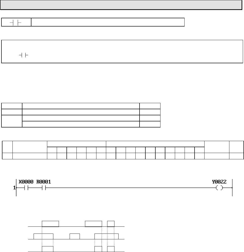
6F3B0253
Basic Hardware and Function 117
7. Instructions
NO contact
Expression
A
Input Output
Function
NO (normally open) contact of device A.
When the input is ON and the device A is ON, the output is turned ON.
Execution condition
Input Operation Output
OFF Regardless of the state of device AOFF
ON When device A is OFF OFF
When device A is ON ON
Operand
Name Device Register Constant Index
X Y R S T. C. XWYWRWSW T C D I J K
ADevice √√√√√√
Example
Coil Y022 comes ON when the devices X000 and R001 are both ON.
X000
R001
Y022
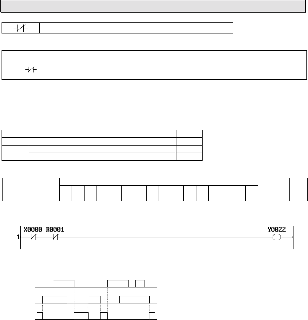
6F3B0253
118 T1-16S User’s Manual
7. Instructions
NC contact
Expression
A
Input Output
Function
NC (normally closed) contact of device A.
When the input is ON and the device A is OFF, the output is turned ON.
Execution condition
Input Operation Output
OFF Regardless of the state of device AOFF
ON When device A is OFF ON
When device A is ON OFF
Operand
Name Device Register Constant Index
X Y R S T. C. XWYWRWSW T C D I J K
ADevice √√√√√√
Example
Coil Y022 comes ON when the devices X000 and R001 are both OFF.
X000
R001
Y022
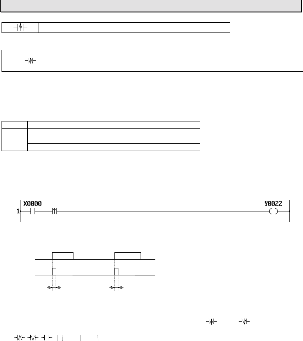
6F3B0253
Basic Hardware and Function 119
7. Instructions
Transitional contact (Rising edge)
Expression
Input Output
Function
When the input at last scan is OFF and the input at this scan is ON, the output is turned ON.
This instruction is used to detect the input changing from OFF to ON.
Execution condition
Input Operation Output
OFF Regardless of the input state at last scan OFF
ON When the input state at last scan is OFF ON
When the input state at last scan is ON OFF
Operand
No operand is required.
Example
Coil Y022 comes ON for only 1 scan when the device X000 comes ON.
X000
Y022
1 scan time 1 scan time
Note
• In case of T1, the maximum usable number in a program is 512. ( and total)
• In case of T1S, the maximum usable number in a program is 2048.
(PN(P)(N)total)
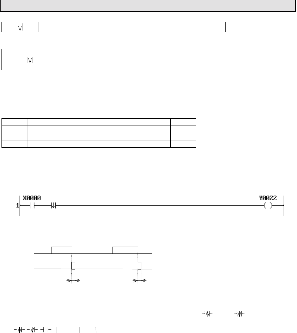
6F3B0253
120 T1-16S User’s Manual
7. Instructions
Transitional contact (Falling edge)
Expression
Input Output
Function
When the input at last scan is ON and the input at this scan is OFF, the output is turned ON.
This instruction is used to detect the input changing from ON to OFF.
Execution condition
Input Operation Output
OFF When the input state at last scan is OFF OFF
When the input state at last scan is ON ON
ON Regardless of the input state at last scan OFF
Operand
No operand is required.
Example
Coil Y022 comes ON for only 1 scan when the device X000 comes OFF.
X000
Y022
1 scan time 1 scan time
Note
• In case of T1, the maximum usable number in a program is 512. ( and total)
• In case of T1S, the maximum usable number in a program is 2048.
(PN(P)(N)total)
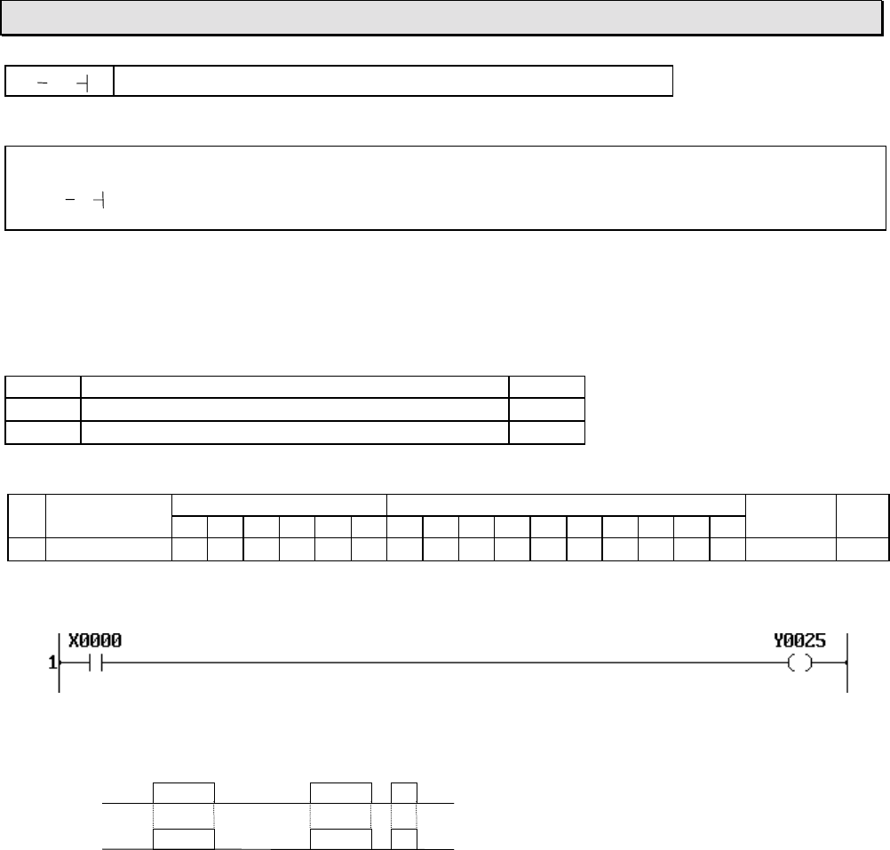
6F3B0253
Basic Hardware and Function 121
7. Instructions
( ) Coil
Expression
A
Input ( )
Function
Relay coil of device A.
When the input is ON, the device A is set to ON.
Execution condition
Input Operation Output
OFF Sets device A to OFF −
ON Sets device A to ON −
Operand
Name Device Register Constant Index
X Y R S T. C. XWYWRWSW T C D I J K
ADevice √√√
Example
Coil Y025 comes ON when the devices X000 is ON.
X000
Y025
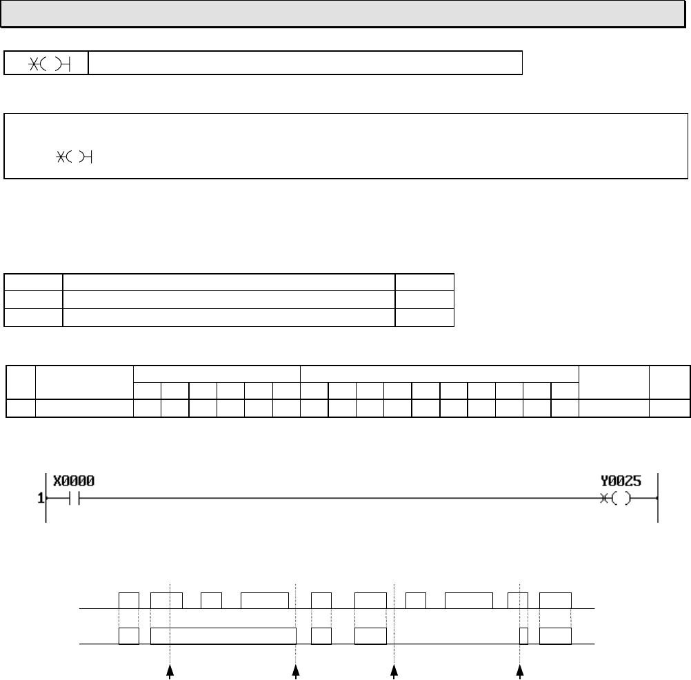
6F3B0253
122 T1-16S User’s Manual
7. Instructions
Forced coil
Expression
A
Input
Function
Regardless of the input sate the state of device A is retained.
Execution condition
Input Operation Output
OFF No operation −
ON No operation −
Operand
Name Device Register Constant Index
X Y R S T. C. XWYWRWSW T C D I J K
ADevice √√√
Example
Device Y025 retains the preceding state regardless of the devices X000 state.
X000
Y025
Set force Reset force Set force Reset force
Note
• The forced coil is a debugging function. The state of a forced coil device can be set ON or OFF
by the programming tool.
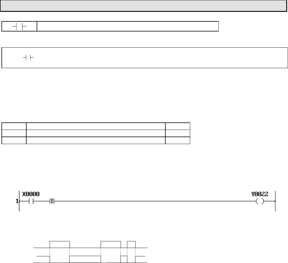
6F3B0253
Basic Hardware and Function 123
7. Instructions
I Inverter
Expression
Input I Output
Function
When the input is OFF, the output is turned ON, and when the input is ON, the output is turned
OFF.
This instruction inverts the link state.
Execution condition
Input Operation Output
OFF Inverts the input state ON
ON Inverts the input state OFF
Operand
No operand is required.
Example
Y022 comes ON when X000 is OFF, and Y022 comes OFF when X000 is ON.
X000
Y022
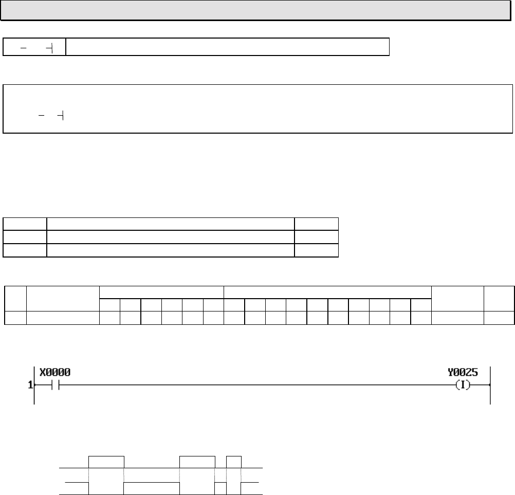
6F3B0253
124 T1-16S User’s Manual
7. Instructions
( I ) Invert coil
Expression
A
Input ( I )
Function
When the input is OFF, the device A is set to ON, and when the input is ON, the device A is set to
OFF. This instruction inverts the input state and store it in the device A.
Execution condition
Input Operation Output
OFF Sets device A to ON −
ON Sets device A to OFF −
Operand
Name Device Register Constant Index
X Y R S T. C. XWYWRWSW T C D I J K
ADevice √√√
Example
Y025 comes ON when X000 is OFF, and Y025 comes OFF when X000 is ON.
X000
Y025

6F3B0253
Basic Hardware and Function 125
7. Instructions
PPositive pulse contact
Expression
A
Input P Output
Function
When the input is ON and the device A is changed from OFF to ON (OFF at last scan and ON at
this scan), the output is turned ON.
This instruction is used to detect the device changing from OFF to ON.
Execution condition
Input Operation Output
OFF Regardless of the state of device AOFF
ON State of device A is OFF OFF
State of device A is ON A is OFF at last scan ON
A is ON at last scan OFF
Operand
Name Device Register Constant Index
X Y R S T. C. XWYWRWSW T C D I J K
ADevice √√√√√√
Example
R100 comes ON for only 1 scan when X000 is ON and X003 changes to ON.
X000
X003
R100
1 scan time 1 scan time
Note
• The maximum usable number in a program is 2048.
(PN(P)(N)total)
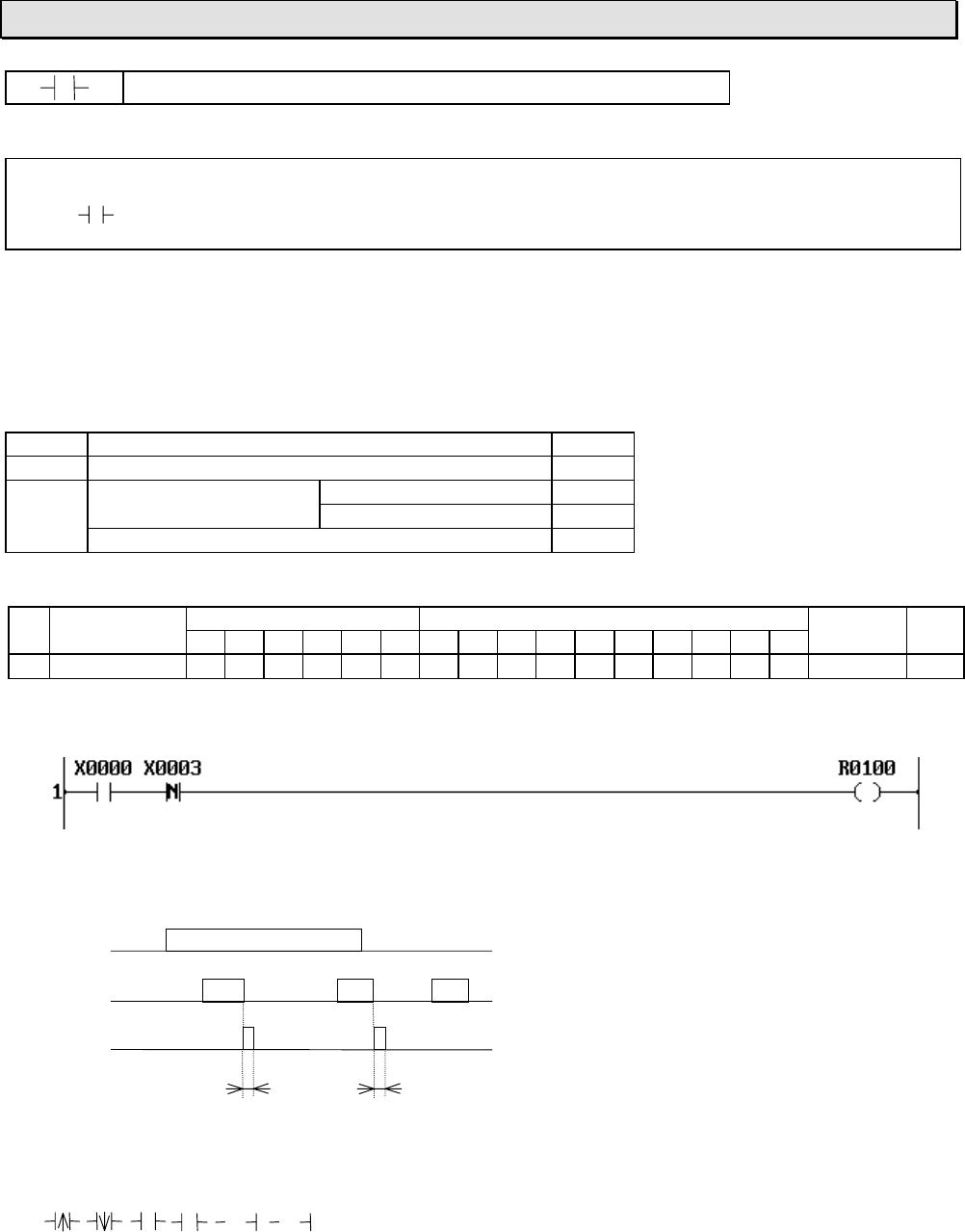
6F3B0253
126 T1-16S User’s Manual
7. Instructions
NNegative pulse contact
Expression
A
Input N Output
Function
When the input is ON and the device A is changed from ON to OFF (ON at last scan and OFF at
this scan), the output is turned ON.
This instruction is used to detect the device changing from ON to OFF.
Execution condition
Input Operation Output
OFF Regardless of the state of device AOFF
ON State of device A is OFF A is OFF at last scan OFF
A is ON at last scan ON
State of device A is ON OFF
Operand
Name Device Register Constant Index
X Y R S T. C. XWYWRWSW T C D I J K
ADevice √√√√√√
Example
R100 comes ON for only 1 scan when X000 is ON and X003 changes to OFF.
X000
X003
R100
1 scan time 1 scan time
Note
• The maximum usable number in a program is 2048.
(PN(P)(N)total)
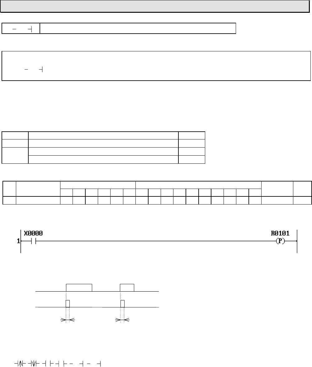
6F3B0253
Basic Hardware and Function 127
7. Instructions
( P ) Positive pulse coil
Expression
A
Input ( P )
Function
When the input is changed form OFF to ON, the device A is set to ON for 1 scan time.
This instruction is used to detect the input changing from OFF to ON.
Execution condition
Input Operation Output
OFF Sets device A to OFF −
ON When the input at last scan is OFF, sets A to ON −
When the input at last scan is ON, sets A to OFF −
Operand
Name Device Register Constant Index
X Y R S T. C. XWYWRWSW T C D I J K
ADevice √√√
Example
R101 comes ON for only 1 scan when X000 is changed from OFF to ON.
X000
R100
1 scan time 1 scan time
Note
• The maximum usable number in a program is 2048.
(PN(P)(N)total)
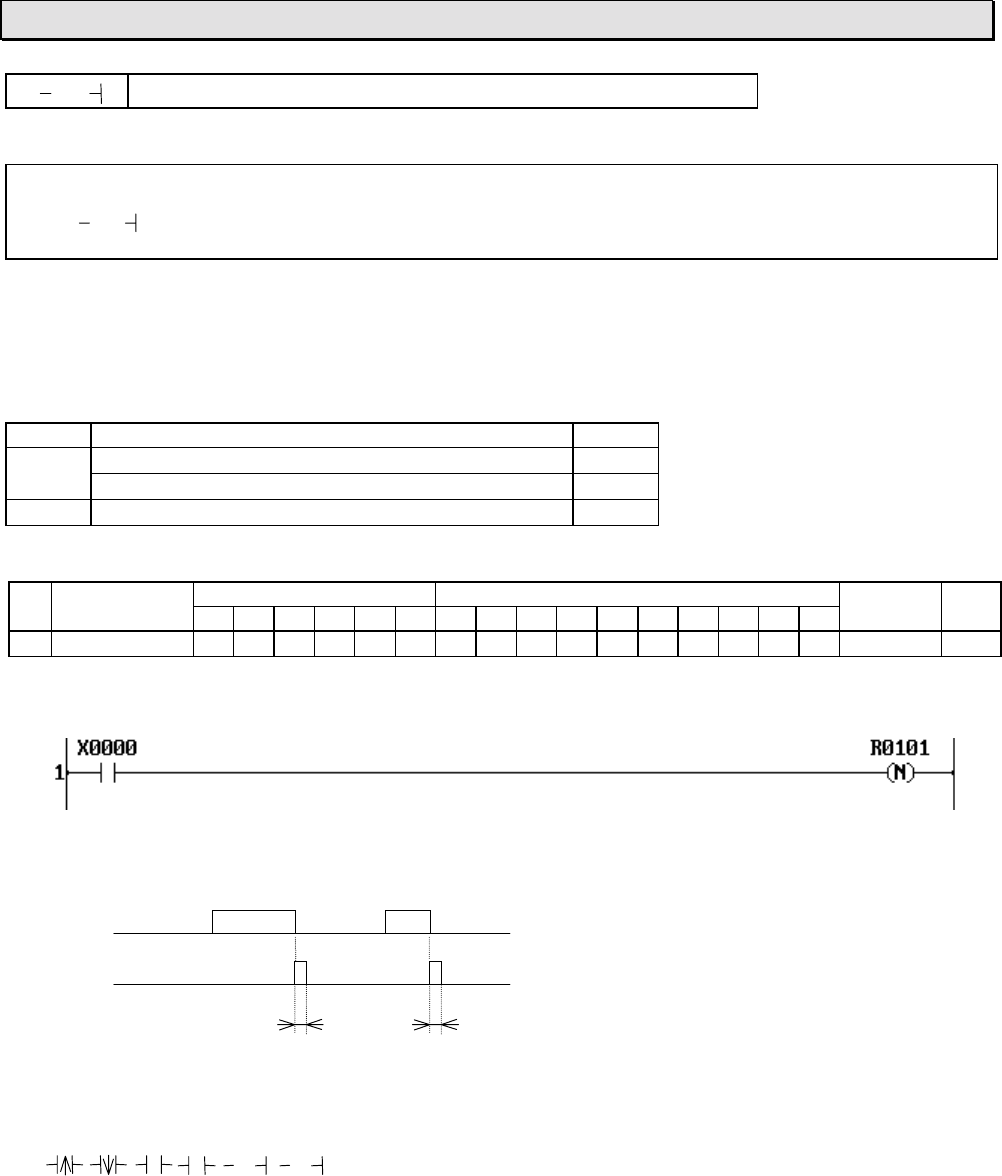
6F3B0253
128 T1-16S User’s Manual
7. Instructions
( N ) Negative pulse coil
Expression
A
Input ( N )
Function
When the input is changed form ON to OFF, the device A is set to ON for 1 scan time.
This instruction is used to detect the input changing from ON to OFF.
Execution condition
Input Operation Output
OFF When the input at last scan is OFF, sets A to OFF −
When the input at last scan is ON, sets A to ON −
ON Sets device A to OFF −
Operand
Name Device Register Constant Index
X Y R S T. C. XWYWRWSW T C D I J K
ADevice √√√
Example
R101 comes ON for only 1 scan when X000 is changed from ON to OFF.
X000
R100
1 scan time 1 scan time
Note
• The maximum usable number in a program is 2048.
(PN(P)(N)total)
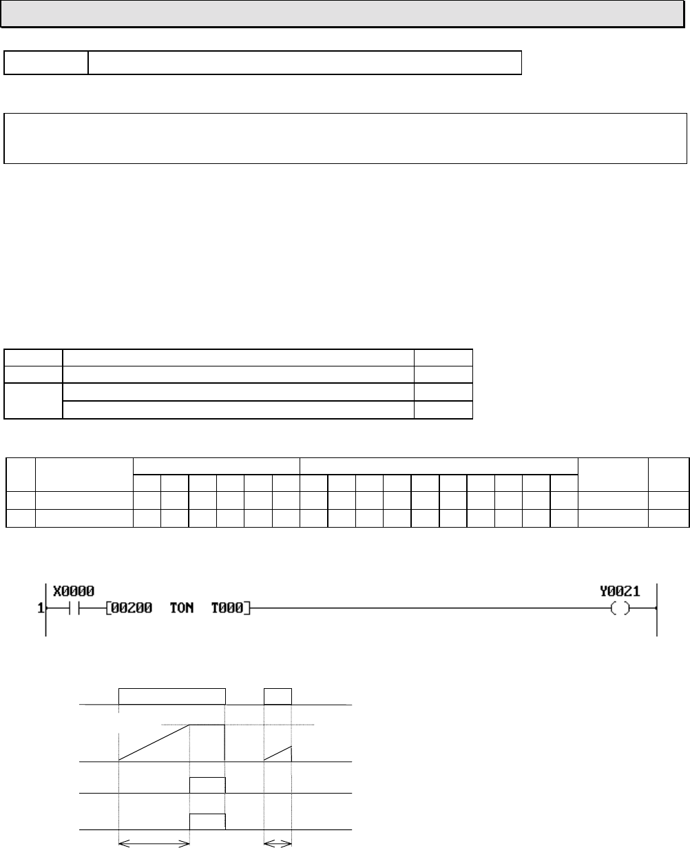
6F3B0253
Basic Hardware and Function 129
7. Instructions
TON ON delay timer
Expression
Input [ A TON B ] Output
Function
When the input is changed from OFF to ON, timer updating for the timer register B is started. The
elapsed time is stored in B. When the specified time by A has elapsed after the input came ON, the
output and the timer device corresponding to B is turned ON. (Timer updating is stopped)
When the input is changed from ON to OFF, B is cleared to 0, and the output and the timer device
are turned OFF.
The available data range for operand A is 0 to 32767.
Execution condition
Input Operation Output
OFF No operation (timer is not updating) OFF
ON Elapsed time < preset time (timer is updating) OFF
Elapsed time ≥ preset time (timer is not updating) ON
Operand
Name Device Register Constant Index
X Y R S T. C. XWYWRWSW T C D I J K
APreset time √√√√√√√√√√
0 - 32767
BElapsed time √
Example
Y021 (and the timer device T.000) is turned ON 2 seconds after X000 came ON.
X000
T000
T.000
Y021
Preset time (2s) Less than preset time
Preset value Note
• Time is set in 10 ms units for;
T1: T000 to T031 (0 to 327.67 s)
T1S: T000 to T063 (0 to 327.67 s)
• Time is set in 100 ms units for;
T1: T032 to T063 (0 to 3276.7 s)
T1S: T064 to T255 (0 to 3276.7 s)
• Multiple timer instructions (TON, TOF or
SS) with the same timer register are not
allowed.
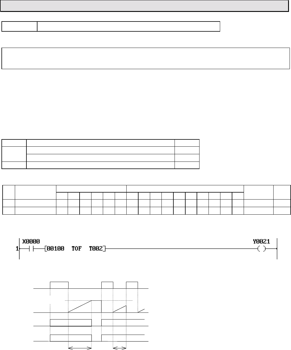
6F3B0253
130 T1-16S User’s Manual
7. Instructions
TOF OFF delay timer
Expression
Input [ A TOF B ] Output
Function
When the input is changed from OFF to ON, the output and the timer device corresponding to the
timer register B are set to ON. When the input is changed from ON to OFF, timer updating for B is
started. The elapsed time is stored in B. When the specified time by A has elapsed after the input
came OFF, the output and the timer device are turned OFF. (Timer updating is stopped)
The available data range for operand A is 0 to 32767.
Execution condition
Input Operation Output
OFF Elapsed time < preset time (timer is updating) ON
Elapsed time ≥ preset time (timer is not updating) OFF
ON No operation (timer is not updating) ON
Operand
Name Device Register Constant Index
X Y R S T. C. XWYWRWSW T C D I J K
APreset time √√√√√√√√√√
0 - 32767
BElapsed time √
Example
Y021 (and the timer device T.002) is turned OFF 1 second after X000 came OFF.
X000
T002
T.002
Y021
Preset time (1 s) Less than preset time
Preset value
Note
• Time is set in 10 ms units for;
T1: T000 to T031 (0 to 327.67 s)
T1S: T000 to T063 (0 to 327.67 s)
• Time is set in 100 ms units for;
T1: T032 to T063 (0 to 3276.7 s)
T1S: T064 to T255 (0 to 3276.7 s)
• Multiple timer instructions (TON, TOF or
SS) with the same timer register are not
allowed.
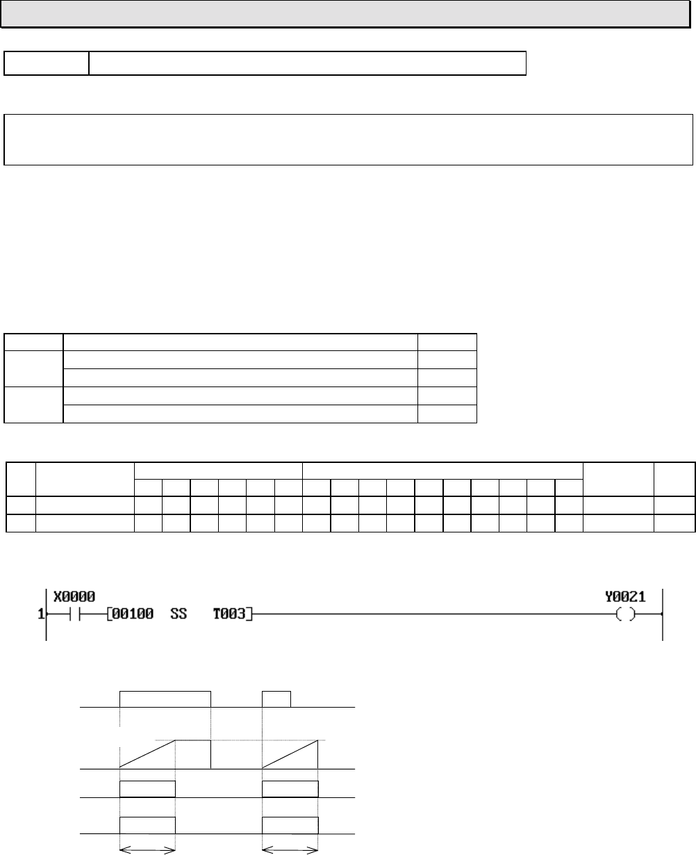
6F3B0253
Basic Hardware and Function 131
7. Instructions
SS Single shot timer
Expression
Input [ A SS B ] Output
Function
When the input is changed from OFF to ON, the output and the timer device corresponding to the
timer register B are set to ON, and timer updating for B is started. The elapsed time is stored in B.
When the specified time by A has elapsed after the input came ON, the output and the timer device
are turned OFF. (Timer updating is stopped)
The available data range for operand A is 0 to 32767.
Execution condition
Input Operation Output
OFF Elapsed time < preset time (timer is updating) ON
Elapsed time ≥ preset time (timer is not updating) OFF
ON Elapsed time < preset time (timer is updating) ON
Elapsed time ≥ preset time (timer is not updating) OFF
Operand
Name Device Register Constant Index
X Y R S T. C. XWYWRWSW T C D I J K
APreset time √√√√√√√√√√
0 - 32767
BElapsed time √
Example
Y021 (and the timer device T.003) is turned OFF 1 second after X000 came ON.
X000
T003
T.003
Y021
Preset time (1 s) Preset time (1 s)
Preset value
Note
• Time is set in 10 ms units for;
T1: T000 to T031 (0 to 327.67 s)
T1S: T000 to T063 (0 to 327.67 s)
• Time is set in 100 ms units for;
T1: T032 to T063 (0 to 3276.7 s)
T1S: T064 to T255 (0 to 3276.7 s)
• Multiple timer instructions (TON, TOF or
SS) with the same timer register are not
allowed.
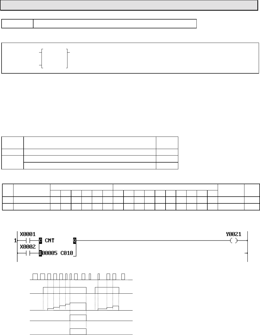
6F3B0253
132 T1-16S User’s Manual
7. Instructions
CNT Counter
Expression
Count input C CNT Q Output
Enable input E A B
Function
While the enable input is ON, this instruction counts the number of the count input changes from
OFF to ON. The count value is stored in the counter register B. When the count value reaches the
set value A, the output and the counter device corresponding to B are turned ON. When the enable
input comes OFF, B is cleared to 0 and the output and the counter device are turned OFF.
The available data range for operand A is 0 to 65535.
Execution condition
Enable
input Operation Output
OFF No operation (B is cleared to 0) OFF
ON Count value (B) < set value (A)OFF
Count value (B) ≥ set value (A)ON
Operand
Name Device Register Constant Index
X Y R S T. C. XWYWRWSW T C D I J K
ASet value √√√√√√√√√√
0 - 65535
BCount value √
Example
X001
X002
C010
C.010
Y021
Note
• No transitional contact is required for the
count input. The count input rising edge is
detected by this instruction.
• For the count input, direct linking to a
connecting point is not allowed. In this
case, insert a dummy contact (always ON
= S04F, etc.) just before the input.
Refer to Note of Shift register FUN 074.
• Multiple counter instructions (CNT) with
3
2
5
4
3
211
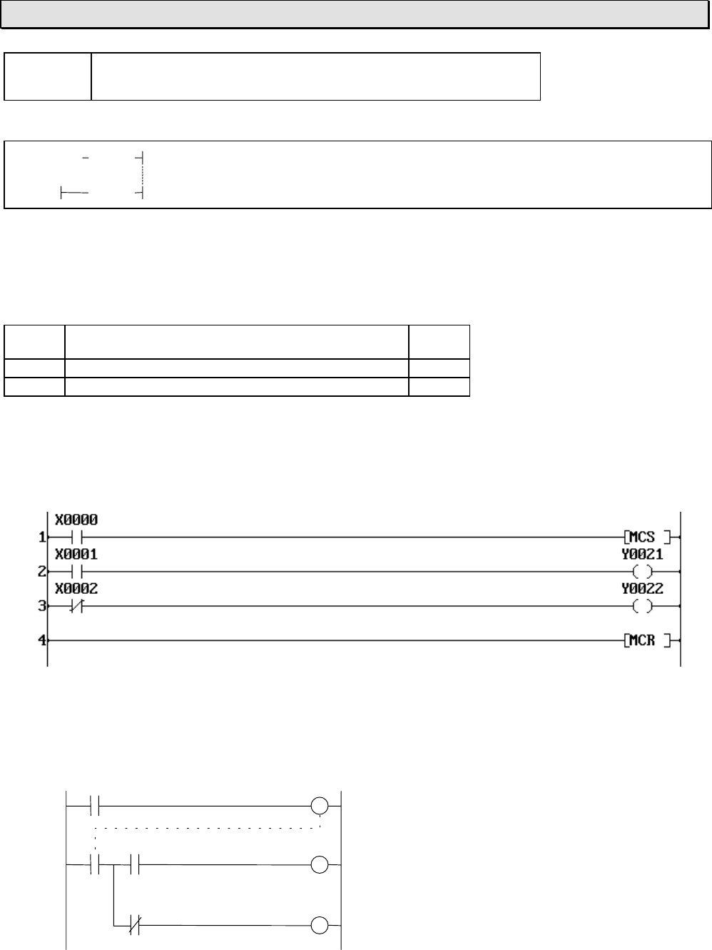
6F3B0253
Basic Hardware and Function 133
7. Instructions
MCS
MCR Master control set / reset
Expression
Input [ MCS ]
[ MCR ]
Function
When the MCS input is ON, ordinary operation is performed. When the MCS input is OFF, the state
of left power rail between MCS and MCR is turned OFF.
Execution condition
MCS
input Operation Output
OFF Sets OFF the left power rail until MCR −
ON Ordinary operation −
Operand
No operand is required.
Example
When X000 is OFF, Y021 and Y022 are turned OFF regardless of the states of X001 and
X002.
Equivalent circuit
X000
X001 Y021
X002 Y022
Note
• MCS and MCR must be used as a pair.
• Nesting is not allowed.
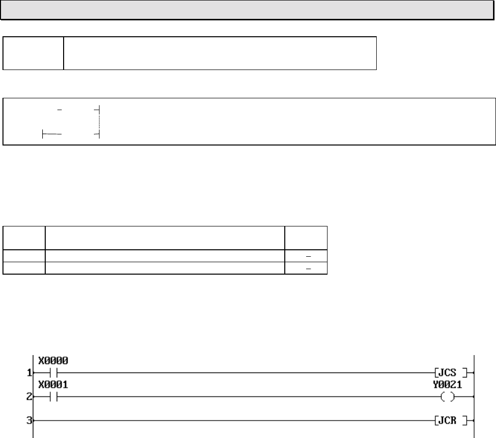
6F3B0253
134 T1-16S User’s Manual
7. Instructions
JCS
JCR Jump control set / reset
Expression
Input [ JCS ]
[ JCR ]
Function
When the JCS input is ON, instructions between JCS and JCR are skipped (not executed). When
the JCS input is OFF, ordinary operation is performed.
Execution condition
JCS
input Operation Output
OFF Ordinary operation
ON Skips until JCR
Operand
No operand is required.
Example
When X000 is ON, the rung 2 circuit is skipped, therefore Y021 is not changed its state
regardless of the X001 state. When X000 is OFF, Y021 is controlled by the X001 state.
Note
• JCS and JCR must be used as a pair.
• Nesting is not allowed.
6F3B0253
Basic Hardware and Function 135
7. Instructions
END End
Expression
[ END ]
Function
Indicates the end of main program or sub-program. Instructions after the END instruction are not
executed. At least one END instruction is necessary in a program.
Execution condition
Input Operation Output
Operand
No operand is required.
Example
Note
• For debugging purpose, 2 or more END instructions can be written in a program.
• Instructions after END instruction are not executed. Those steps are, however, counted as used
steps.
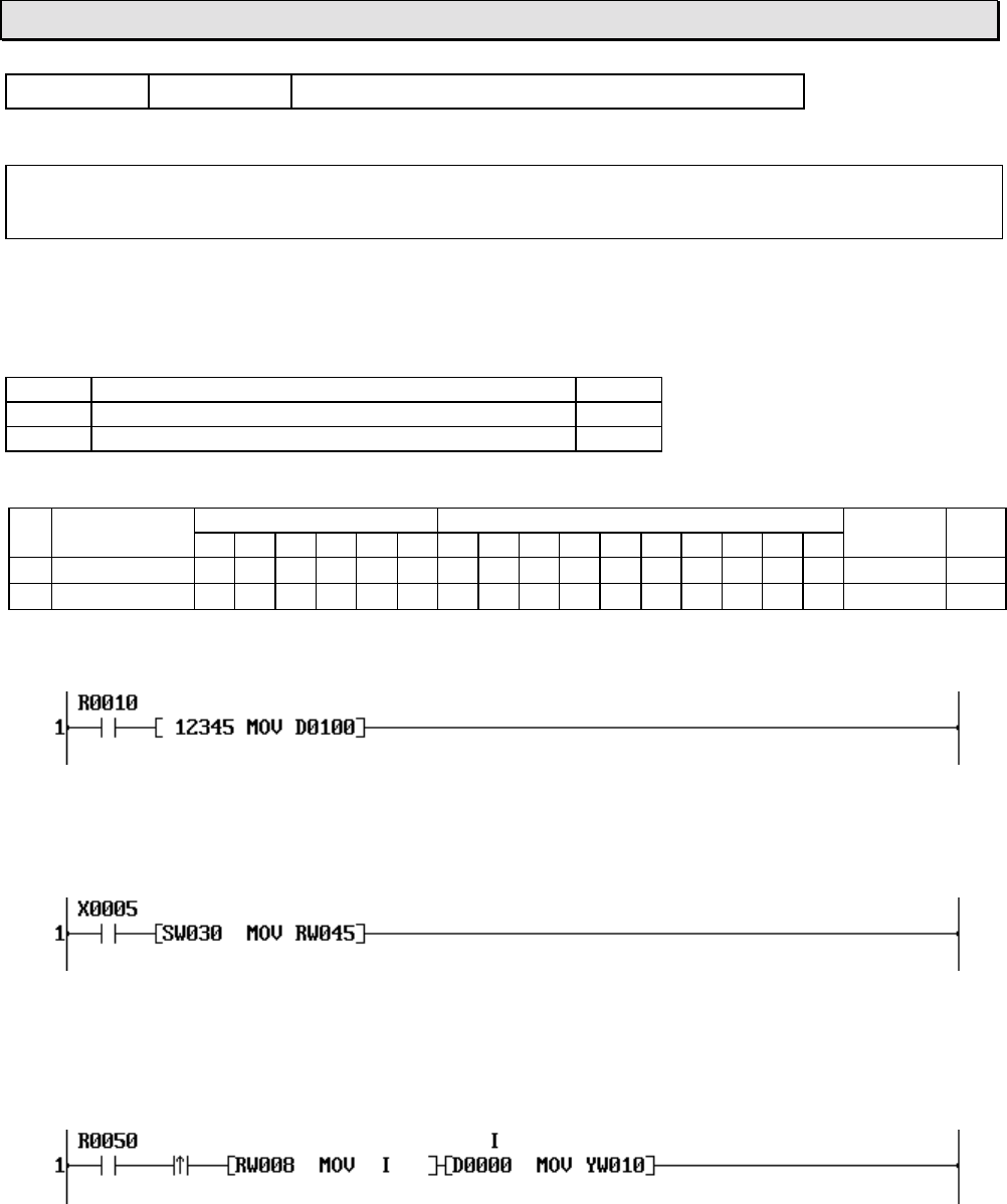
6F3B0253
136 T1-16S User’s Manual
7. Instructions
FUN 018 MOV Data transfer
Expression
Input −[ A MOV B ]− Output
Function
When the input is ON, the data of A is stored in B.
Execution condition
Input Operation Output
OFF No execution OFF
ON Execution ON
Operand
Name Device Register Constant Index
X Y R S T. C. XWYWRWSW T C D I J K
ASource √√√√√√√√√√ √ √
BDestination √√√√√√√√√ √
Example 1 (constant to register)
When R010 is ON, a constant data (12345) is stored in D0100 and the output is turned ON.
Example 2 (register to register)
When X005 is ON, the data of SW30 is stored in RW45 and the output is turned ON. If SW30
is 500, the data 500 is stored in RW45.
Example 3 (index modification)
When R050 is changed from OFF to ON, the data of RW08 is stored in the index register I and
the data of D(0000+I) is stored in YW10. If RW08 is 300, the data of D0300 is stored in YW10.
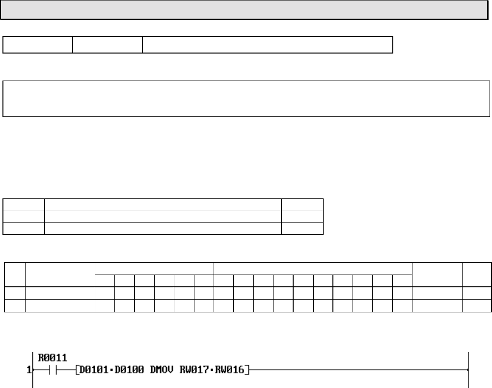
6F3B0253
Basic Hardware and Function 137
7. Instructions
FUN 019 DMOV Double-word data transfer
Expression
Input −[ A+1⋅A MOV B+1⋅B ]− Output
Function
When the input is ON, the double-word (32-bit) data of A+1⋅A is stored in double-word register
B+1⋅B. The data range is -2147483648 to 2147483647.
Execution condition
Input Operation Output
OFF No execution OFF
ON Execution ON
Operand
Name Device Register Constant Index
X Y R S T. C. XWYWRWSW T C D I J K
ASource √√√√√√√√√√ √ √
BDestination √√√√√√√√√ √
Example
When R011 is ON, a double-word data of D0101⋅D0100 is stored in RW17⋅RW16 and the
output is turned ON. If D0101⋅D0100 is 1234567, the data 1234567 is stored in RW17⋅RW16.
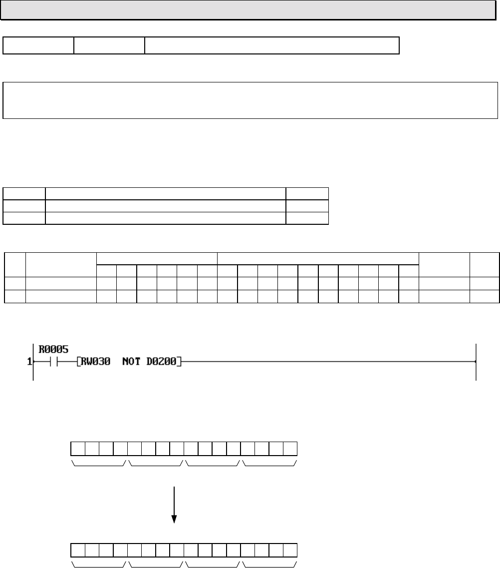
6F3B0253
138 T1-16S User’s Manual
7. Instructions
FUN 020 NOT Invert transfer
Expression
Input −[ A NOT B ]− Output
Function
When the input is ON, the bit-inverted data of A is stored in B.
Execution condition
Input Operation Output
OFF No execution OFF
ON Execution ON
Operand
Name Device Register Constant Index
X Y R S T. C. XWYWRWSW T C D I J K
ASource √√√√√√√√√√ √ √
BDestination √√√√√√√√√ √
Example
When R010 is ON, the bit-inverted data of RW30 is stored in D0200 and the output is turned
ON. If RW30 is H4321, the bit-inverted data (HBCDE) is stored in D0200.
FEDCBA9876543210
RW30 0100001100100001
4321
Bit-invert
FEDCBA9876543210
D0200 1011110011011110
BCDE
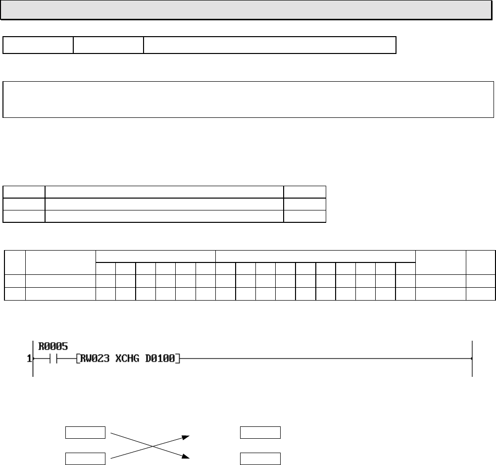
6F3B0253
Basic Hardware and Function 139
7. Instructions
FUN 022 XCHG Data exchange
Expression
Input −[ A XCHG B ]− Output
Function
When the input is ON, the data of A and the data of B is exchanged.
Execution condition
Input Operation Output
OFF No execution OFF
ON Execution ON
Operand
Name Device Register Constant Index
X Y R S T. C. XWYWRWSW T C D I J K
AOperation data √√√√√√√√√ √
BOperation data √√√√√√√√√ √
Example
When R005 is ON, the data of RW23 and D0100 is exchanged. If the original data of RW23 is
23456 and that of D0100 is 291, the operation result is as follows.
RW23 23456 RW23 291
D0100 291 D0100 23456
Before operation After operation
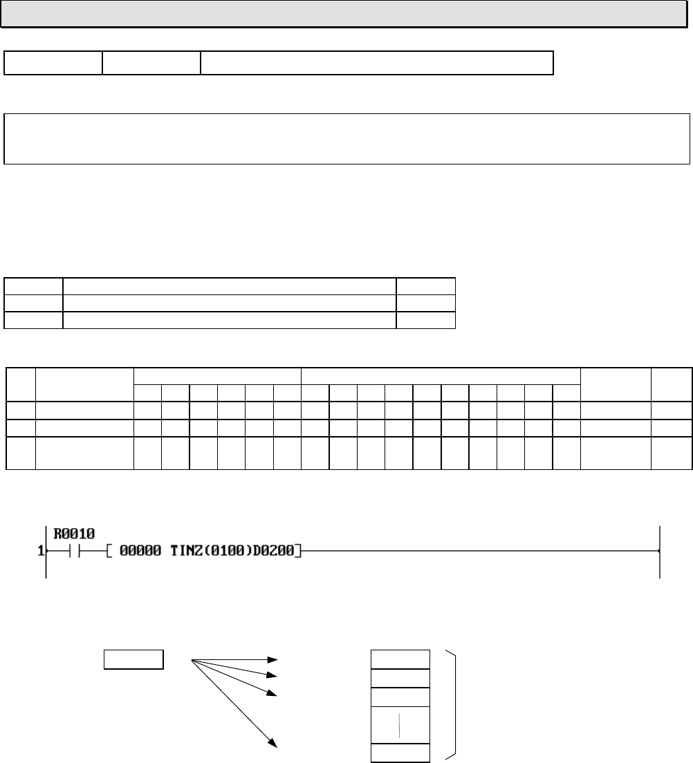
6F3B0253
140 T1-16S User’s Manual
7. Instructions
FUN 024 TINZ Table initialize
Expression
Input −[ A TINZ (n) B ]− Output
Function
When the input is ON, the data of A is stored in n registers starting with B.
The allowable range of the table size n is 1 to 1024 words.
Execution condition
Input Operation Output
OFF No execution OFF
ON Execution ON
Operand
Name Device Register Constant Index
X Y R S T. C. XWYWRWSW T C D I J K
ASource √√√√√√√√√√ √
nTable size 1 - 1024
BStart of
destination √√√√√√
Example
When R010 is ON, a constant data (0) is stored in 100 registers starting with D0200 (D0200 to
D0299) and the output is turned ON.
Constant 0 D0200 0
D0201 0
D0202 0 100 registers
D0299 0
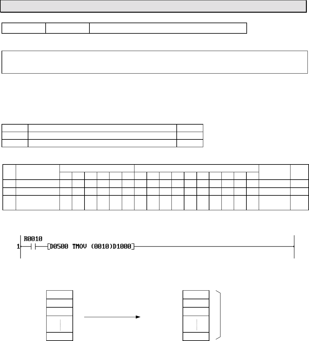
6F3B0253
Basic Hardware and Function 141
7. Instructions
FUN 025 TMOV Table transfer
Expression
Input −[ A TMOV (n) B ]− Output
Function
When the input is ON, the data of n registers starting with A are transferred to n registers starting
with B in a block. The allowable range of the table size n is 1 to 1024 words.
Execution condition
Input Operation Output
OFF No execution OFF
ON Execution ON
Operand
Name Device Register Constant Index
X Y R S T. C. XWYWRWSW T C D I J K
AStart of source √√√√√√√
nTable size 1 - 1024
BStart of
destination √√√√√√
Example
When R010 is ON, the data of D0500 to D0509 (10 registers) are block transferred to D1000 to
D1009, and the output is turned ON.
D0500 1111 D1000 1111
D0501 2222 D1001 2222
D0502 3333 Block transfer D1002 3333 10 registers
D0509 12345 D1009 12345
Note
• The source and destination tables can be overlapped.
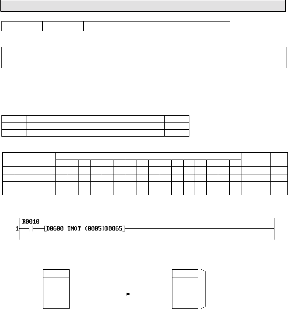
6F3B0253
142 T1-16S User’s Manual
7. Instructions
FUN 026 TNOT Table invert transfer
Expression
Input −[ A TNOT (n) B ]− Output
Function
When the input is ON, the data of n registers starting with A are bit-inverted and transferred to n
registers starting with B in a block. The allowable range of the table size n is 1 to 1024 words.
Execution condition
Input Operation Output
OFF No execution OFF
ON Execution ON
Operand
Name Device Register Constant Index
X Y R S T. C. XWYWRWSW T C D I J K
AStart of source √√√√√√√
nTable size 1 - 1024
BStart of
destination √√√√√√
Example
When R010 is ON, the data of D0600 to D0604 (5 registers) are bit-inverted and transferred to
D0865 to D0869, and the output is turned ON.
D0600 H00FF D0865 HFF00
D0601 H0000 Bit-invert D0866 HFFFF
D0602 H1234 and transfer D0867 HEDCB 5 registers
D0603 H5555 D0868 HAAAA
D0604 H89AB D0869 H7654
Note
• The source and destination tables can be overlapped.

6F3B0253
Basic Hardware and Function 143
7. Instructions
FUN 027 + Addition
Expression
Input −[ A + B → C ]− Output
Function
When the input is ON, the data of A and the data of B are added, and the result is stored in C.
If the result is greater than 32767, the upper limit value 32767 is stored in C, and the output is
turned ON. If the result is smaller than -32768, the lower limit value -32768 is stored in C, and the
output is turned ON.
Execution condition
Input Operation Output
OFF No execution OFF
ON Execution (normal) OFF
Execution (overflow or underflow occurred) ON
Operand
Name Device Register Constant Index
X Y R S T. C. XWYWRWSW T C D I J K
AAugend √√√√√√√√√√ √ √
BAddend √√√√√√√√√√ √ √
CSum √√√√√√√√√ √
Example
When R005 is ON, the data of D0100 and the constant data 1000 is added, and the result is
stored in D0110.
If the data of D0100 is 12345, the result 13345 is stored in D0110, and R010 is turned OFF.
D0100 12345 +D0110 13345 R010 is OFF
Constant 1000
If the data of D0100 is 32700, the result exceeds the limit value, therefore 32767 is stored in
D0110, and R010 is turned ON.
D0100 32700 Overflow
+D0110 32767 R010 is ON
Constant 1000
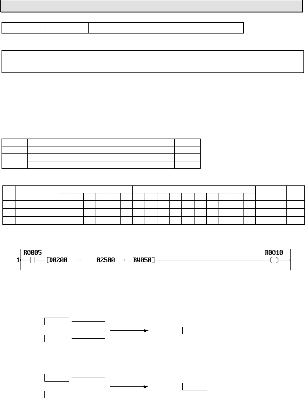
6F3B0253
144 T1-16S User’s Manual
7. Instructions
FUN 028 −Subtraction
Expression
Input −[ A − B → C ]− Output
Function
When the input is ON, the data of B is subtracted from the data of A, and the result is stored in C.
If the result is greater than 32767, the upper limit value 32767 is stored in C, and the output is
turned ON. If the result is smaller than -32768, the lower limit value -32768 is stored in C, and the
output is turned ON.
Execution condition
Input Operation Output
OFF No execution OFF
ON Execution (normal) OFF
Execution (overflow or underflow occurred) ON
Operand
Name Device Register Constant Index
X Y R S T. C. XWYWRWSW T C D I J K
AMinuend √√√√√√√√√√ √ √
BSubtrahend √√√√√√√√√√ √ √
CDifference √√√√√√√√√ √
Example
When R005 is ON, the constant data 2500 is subtracted from the data of D0200, and the result
is stored in RW50.
If the data of D0200 is 15000, the result 12500 is stored in RW50, and R010 is turned OFF.
D0200 15000 −RW50 12500 R010 is OFF
Constant 2500
If the data of D0200 is -31000, the result is smaller than the limit value, therefore -32768 is
stored in RW50, and R010 is turned ON.
D0100 -31000 Underflow
−RW50 -32768 R010 is ON
Constant 2500
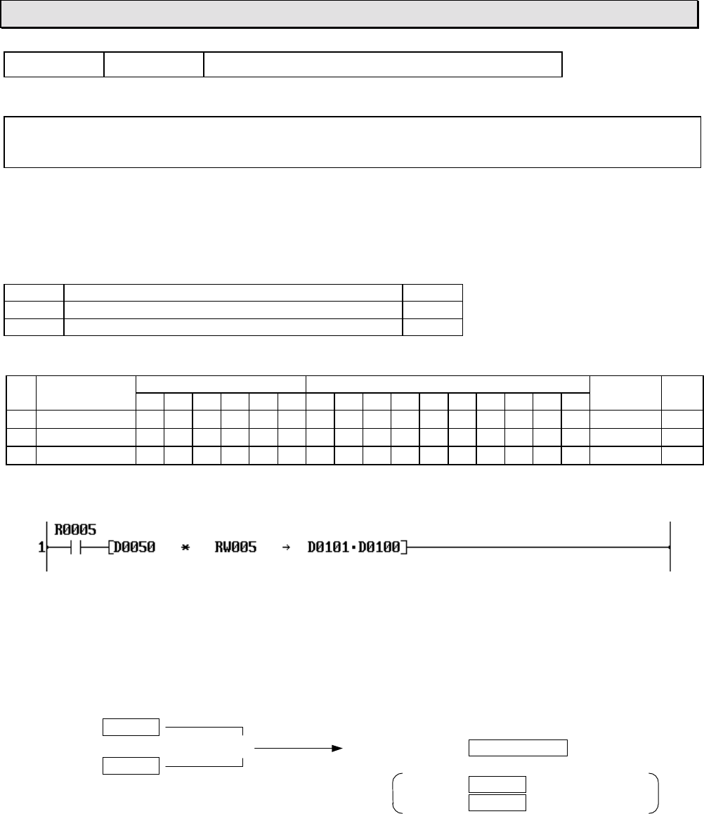
6F3B0253
Basic Hardware and Function 145
7. Instructions
FUN 029 ∗Multiplication
Expression
Input −[ A ∗ B → C+1
⋅
C ]− Output
Function
When the input is ON, the data of A is multiplied by the data of B, and the result is stored in
double-length register C+1
⋅
C.
Execution condition
Input Operation Output
OFF No execution OFF
ON Execution ON
Operand
Name Device Register Constant Index
X Y R S T. C. XWYWRWSW T C D I J K
AMultiplicand √√√√√√√√√√ √ √
BMultiplier √√√√√√√√√√ √ √
CProduct √√√√√√√√ √
Example
When R005 is ON, the data of D0050 is multiplied by the data of RW05, and the result is
stored in double-length register D0101⋅D0100 (upper 16-bit in D0101 and lower 16-bit in
D0100).
If the data of D0050 is 1500 and the data of RW05 is 20, the result 30000 is stored in
D0101⋅D0100.
D0050 1500 ×D0101⋅D0100 30000
RW05 20 D0101 H0000 (upper 16-bit)
D0100 H7530 (lower 16-bit)
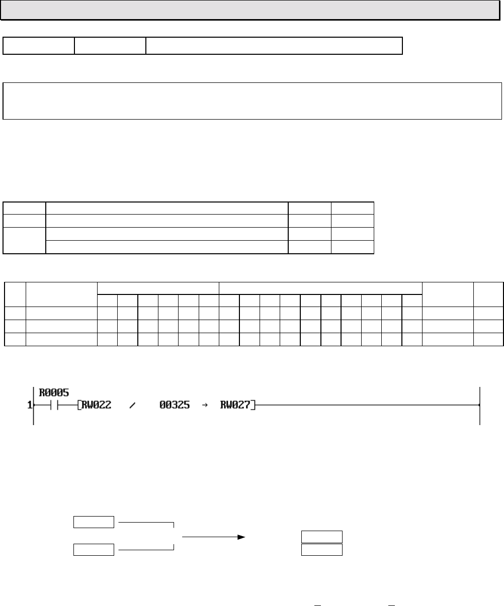
6F3B0253
146 T1-16S User’s Manual
7. Instructions
FUN 030 / Division
Expression
Input −[ A / B → C ]− Output
Function
When the input is ON, the data of A is divided by the data of B, and the quotient is stored in C and
the remainder in C+1.
Execution condition
Input Operation Output ERF
OFF No execution OFF −
ON Normal execution (B ≠ 0) ON −
No execution (B = 0) OFF Set
Operand
Name Device Register Constant Index
X Y R S T. C. XWYWRWSW T C D I J K
ADividend √√√√√√√√√√ √ √
BDivisor √√√√√√√√√√ √ √
CQuotient √√√√√√√√√ √
Example
When R005 is ON, the data of RW22 is divided by the constant data 325, and the quotient is
stored in RW27 and the remainder is stored in RW28.
If the data of RW22 is 2894, the quotient 8 is stored in RW27 and the remainder 294 is stored
in RW28.
RW22 2894 ÷RW27 8 (quotient)
Constant 325 RW28 294 (remainder)
Note
• If divisor (operand B) is 0, ERF (instruction error flag = S051) is set to ON.
The ERF (S051) can be reset to OFF by user program, e.g. [ RST S051 ] .
• If the index register K is used as operand C, the remainder is ignored.
• If operand A is -32768 and operand B is -1, the data -32768 is stored in C and 0 is stored in
C+1.
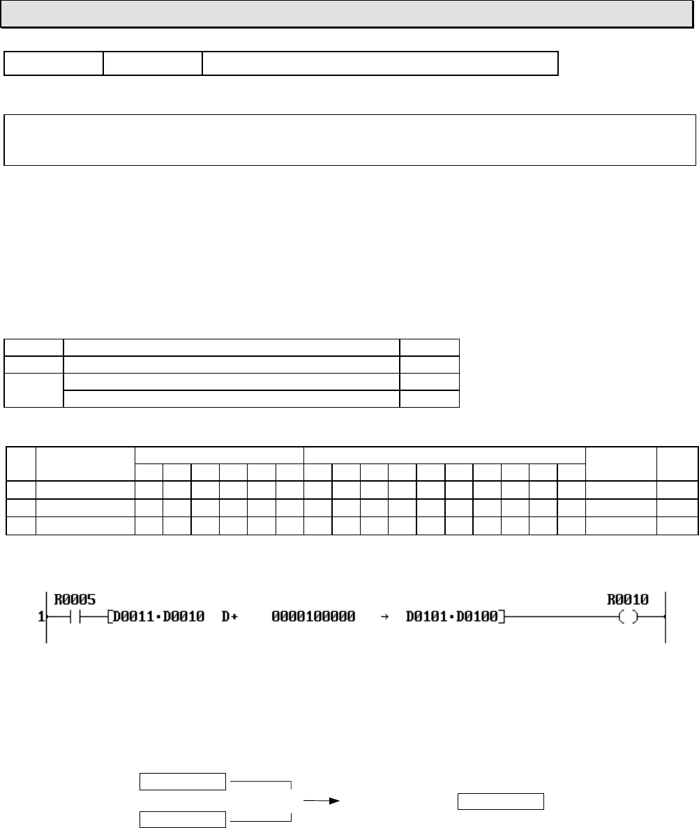
6F3B0253
Basic Hardware and Function 147
7. Instructions
FUN 031 D+ Double-word addition
Expression
Input −[ A+1⋅A D+ B+1⋅B → C+1⋅C ]− Output
Function
When the input is ON, the double-word data of A+1⋅A and B+1⋅B are added, and the result is
stored in C+1⋅C. The data range is -2147483648 to 2147483647.
If the result is greater than 2147483647, the upper limit value 2147483647 is stored in C+1⋅C, and
the output is turned ON. If the result is smaller than -2147483648, the lower limit value
-2147483648 is stored in C+1⋅C, and the output is turned ON.
Execution condition
Input Operation Output
OFF No execution OFF
ON Execution (normal) OFF
Execution (overflow or underflow occurred) ON
Operand
Name Device Register Constant Index
X Y R S T. C. XWYWRWSW T C D I J K
AAugend √√√√√√√ √
BAddend √√√√√√√ √
CSum √√√√√√
Example
When R005 is ON, the data of D0011⋅D0010 and the constant data 100000 is added, and the
result is stored in D0101⋅D0100.
If the data of D0011⋅D0010 is 300000, the result 400000 is stored in D0101⋅D0100, and R010
is turned OFF. (No overflow/underflow)
D0011⋅D0010 300000 +D0101⋅D0100 400000 R010 is OFF
Constant 100000
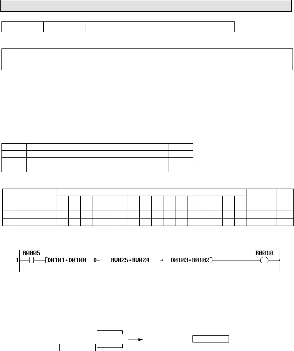
6F3B0253
148 T1-16S User’s Manual
7. Instructions
FUN 032 D−Double-word subtraction
Expression
Input −[ A+1⋅A D− B+1⋅B → C+1⋅C ]− Output
Function
When the input is ON, the double-word data of B+1⋅B is subtracted from A+1⋅A, and the result is
stored in C+1⋅C. The data range is -2147483648 to 2147483647.
If the result is greater than 2147483647, the upper limit value 2147483647 is stored in C+1⋅C, and
the output is turned ON. If the result is smaller than -2147483648, the lower limit value
-2147483648 is stored in C+1⋅C, and the output is turned ON.
Execution condition
Input Operation Output
OFF No execution OFF
ON Execution (normal) OFF
Execution (overflow or underflow occurred) ON
Operand
Name Device Register Constant Index
X Y R S T. C. XWYWRWSW T C D I J K
AMinuend √√√√√√√ √
BSubtrahend √√√√√√√ √
CDifference √√√√√√
Example
When R005 is ON, the double-word data of RW25⋅RW24 is subtracted from the double-word
data of D0101⋅D0100, and the result is stored in D0103⋅D0102.
If the data of D0101⋅D0100 is 1580000 and the data of RW25⋅RW24 is 80000, the result
1500000 is stored in D0103⋅D0102, and R010 is turned OFF. (No overflow/underflow)
D0101⋅D0100 1580000 −D0103⋅D0102 1500000 R010 is OFF
RW25⋅RW24 80000

6F3B0253
Basic Hardware and Function 149
7. Instructions
FUN 035 +C Addition with carry
Expression
Input −[ A +C B → C ]− Output
Function
When the input is ON, the data of A, B and the carry flag (CF = S050) are added, and the result is
stored in C. If carry is occurred in the operation, the carry flag is set to ON. If the result is greater
than 32767 or smaller than -32768, the output is turned ON.
This instruction is used to perform unsigned addition or double-length addition.
Execution condition
Input Operation Output CF
OFF No execution OFF −
ON Execution Normal No carry OFF Reset
Carry occurred OFF Set
Overflow / No carry ON Reset
underflow Carry occurred ON Set
Operand
Name Device Register Constant Index
X Y R S T. C. XWYWRWSW T C D I J K
AAugend √√√√√√√√√√ √ √
BAddend √√√√√√√√√√ √ √
CSum √√√√√√√√√ √
Example
When R013 is ON, the data of double-length registers D0101⋅D0100 and RW21⋅RW20 are
added, and the result is stored in D0201⋅D0200. The RSTC is a instruction to reset the carry
flag before starting the calculation.
If the data of D0101⋅D0100 is 12345678 and RW21⋅RW20 is 54322, the result 12400000 is
stored in D0201⋅D0200.
D0101⋅D0100 12345678 +D0201⋅D0200 12400000
RW21⋅RW20 54322
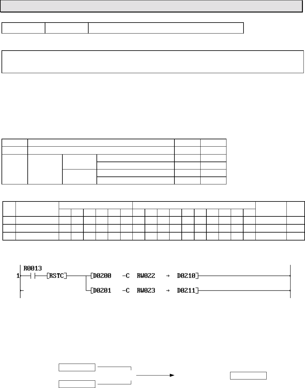
6F3B0253
150 T1-16S User’s Manual
7. Instructions
FUN 036 -C Subtraction with carry
Expression
Input −[ A -C B → C ]− Output
Function
When the input is ON, the data of B and the carry flag (CF = S050) are subtracted from A, and the
result is stored in C. If borrow is occurred in the operation, the carry flag is set to ON. If the result is
greater than 32767 or smaller than -32768, the output is turned ON.
This instruction is used to perform unsigned subtraction or double-length subtraction.
Execution condition
Input Operation Output CF
OFF No execution OFF −
ON Execution Normal No borrow OFF Reset
Borrow occurred OFF Set
Overflow / No borrow ON Reset
underflow Borrow occurred ON Set
Operand
Name Device Register Constant Index
X Y R S T. C. XWYWRWSW T C D I J K
AMinuend √√√√√√√√√√ √ √
BSubtrahend √√√√√√√√√√ √ √
CDifference √√√√√√√√√ √
Example
When R013 is ON, the data of double-length register RW23⋅RW22 is subtracted from the data
of D0201⋅D0200, and the result is stored in D0211⋅D0210. The RSTC is a instruction to reset
the carry flag before starting the calculation.
If the data of D0201⋅D0200 is 12345678 and RW23⋅RW22 is 12340000, the result 5678 is
stored in D0211⋅D0210.
D0201⋅D0200 12345678
-D0211⋅D0210 5678
RW23⋅RW22 12340000
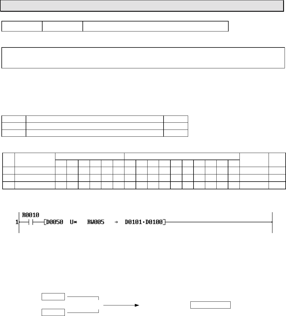
6F3B0253
Basic Hardware and Function 151
7. Instructions
FUN 039 U∗Unsigned multiplication
Expression
Input −[ A U∗ B → C+1
⋅
C ]− Output
Function
When the input is ON, the unsigned data of A and B are multiplied, and the result is stored in
double-length register C+1
⋅
C. The data range of A and B is 0 to 65535 (unsigned 16-bit data)
Execution condition
Input Operation Output
OFF No execution OFF
ON Execution ON
Operand
Name Device Register Constant Index
X Y R S T. C. XWYWRWSW T C D I J K
AMultiplicand √√√√√√√√√√ √ √
BMultiplier √√√√√√√√√√ √ √
CProduct √√√√√√√√ √
Example
When R010 is ON, the data of D0050 is multiplied by the data of RW05, and the result is
stored in double-length register D0101⋅D0100 (upper 16-bit in D0101 and lower 16-bit in
D0100).
If the data of D0050 is 52500 and the data of RW05 is 30, the result 1575000 is stored in
D0101⋅D0100.
D0050 52500 ×D0101⋅D0100 1575000
RW05 30
Note
• This instruction handles the register data as unsigned integer.
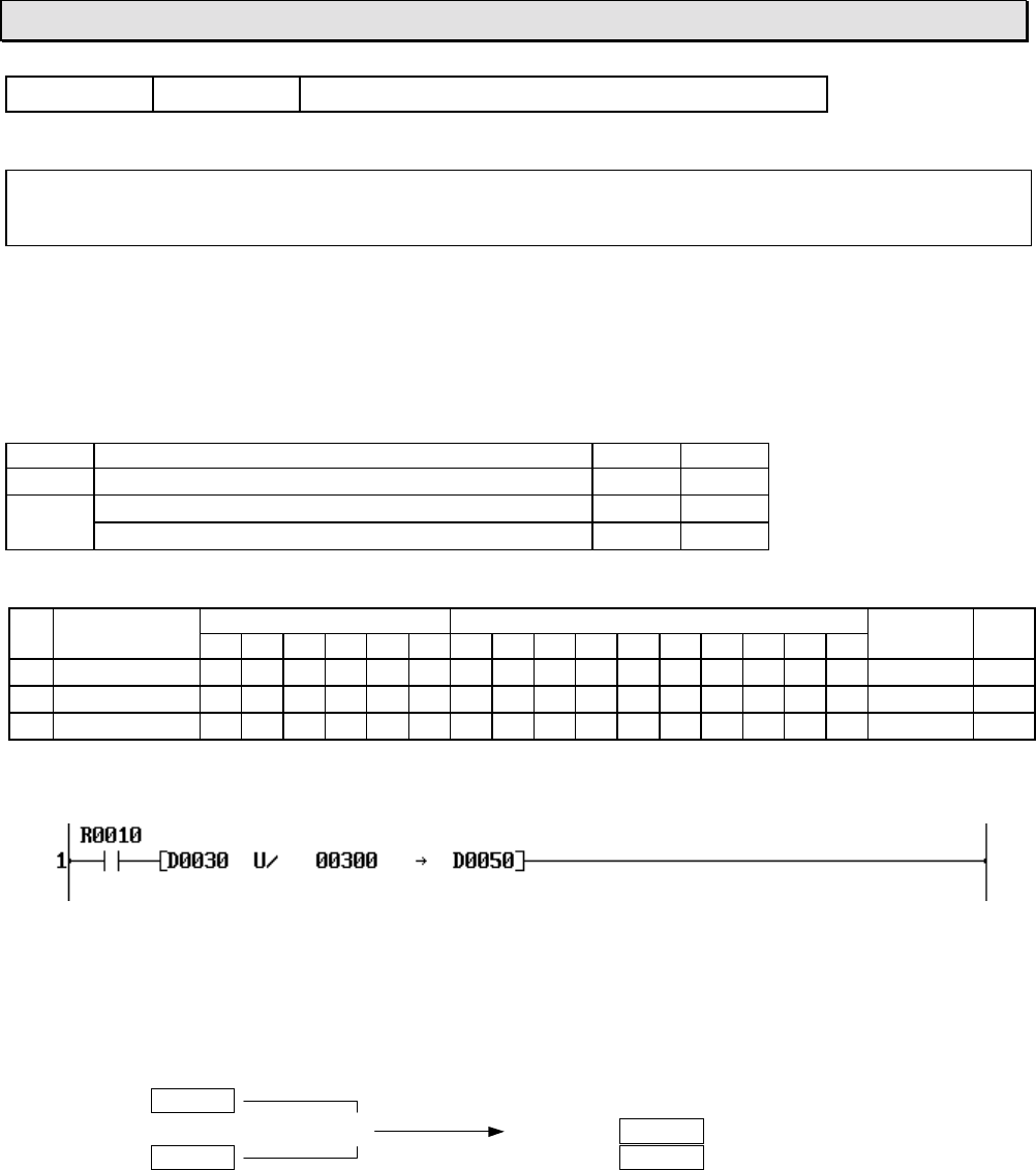
6F3B0253
152 T1-16S User’s Manual
7. Instructions
FUN 040 U/ Unsigned division
Expression
Input −[ A U/ B → C ]− Output
Function
When the input is ON, the unsigned data of A is divided by the unsigned data of B, and the
quotient is stored in C and the remainder in C+1.
The data range of A and B is 0 to 65535 (unsigned 16-bit data)
Execution condition
Input Operation Output ERF
OFF No execution OFF −
ON Normal execution (B ≠ 0) ON −
No execution (B = 0) OFF Set
Operand
Name Device Register Constant Index
X Y R S T. C. XWYWRWSW T C D I J K
ADividend √√√√√√√√√√ √ √
BDivisor √√√√√√√√√√ √ √
CQuotient √√√√√√√√√ √
Example
When R010 is ON, the data of D0030 is divided by the constant data 300, and the quotient is
stored in D0050 and the remainder is stored in D0051.
If the data of D0030 is 54321, the quotient 181 is stored in D0050 and the remainder 21 is
stored in D0051.
D0030 54321 ÷RW27 181 (quotient)
Constant 300 RW28 21 (remainder)
Note
• If divisor (operand B) is 0, ERF (instruction error flag = S051) is set to ON.
The ERF (S051) can be reset to OFF by user program, e.g. −[ RST S051 ]−.
• If the index register K is used as operand C, the remainder is ignored.
• This instruction handles the register data as unsigned integer.
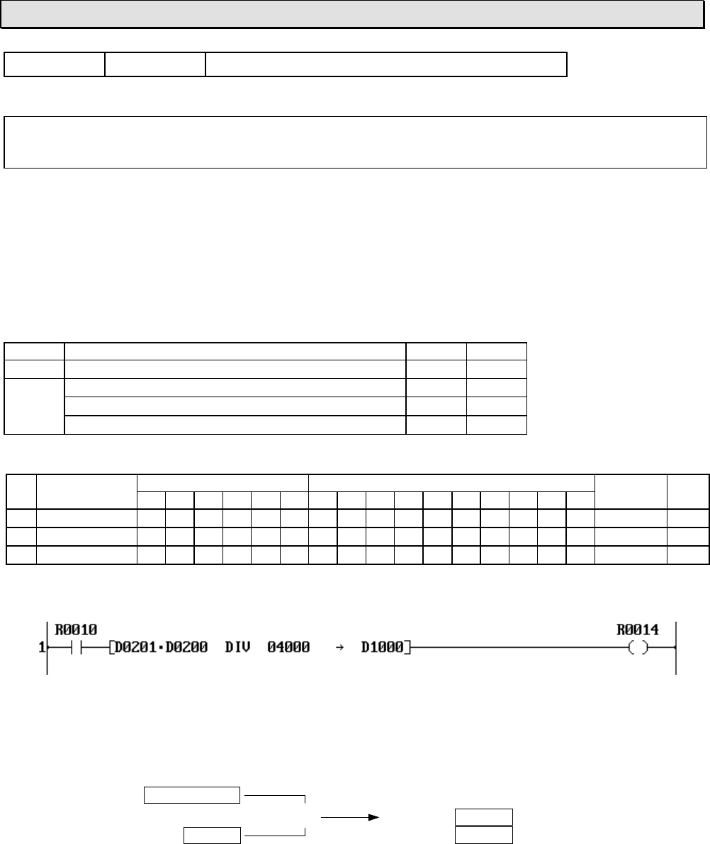
6F3B0253
Basic Hardware and Function 153
7. Instructions
FUN 041 DIV Unsigned double/single division
Expression
Input −[ A+1⋅A DIV B → C ]− Output
Function
When the input is ON, the double-word data of A+1⋅A is divided by the data of B, and the quotient
is stored in C and the remainder in C+1. The data range of A+1⋅A is 0 to 4294967295, and the data
range of B and C is 0 to 65535.
If the quotient is greater than 65535 (overflow), the limit value 65535 is stored in C, 0 is stored in
C+1, and the instruction error flag (ERF = S051) is set to ON.
Execution condition
Input Operation Output ERF
OFF No execution OFF −
ON Normal execution (B ≠ 0) ON −
Overflow (B ≠ 0) ON Set
No execution (B = 0) OFF Set
Operand
Name Device Register Constant Index
X Y R S T. C. XWYWRWSW T C D I J K
ADividend √√√√√√√ √
BDivisor √√√√√√√ √
CQuotient √√√√√√
Example
When R010 is ON, the double-word data of D0201⋅D0200 is divided by the constant data
4000, and the quotient is stored in D1000 and the remainder is stored in D1001.
If the data of D0201⋅D0200 is 332257, the quotient 83 is stored in D1000 and the remainder
257 is stored in D1001.
D0201⋅D0200 332257 ÷D1000 83 (quotient)
Constant 4000 D1001 257 (remainder)
Note
• If divisor (operand B) is 0, ERF (instruction error flag = S051) is set to ON.
The ERF (S051) can be reset to OFF by user program, e.g. −[ RST S051 ]−.
• This instruction handles the register data as unsigned integer.
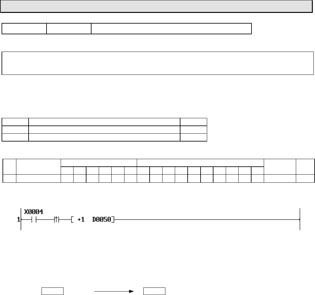
6F3B0253
154 T1-16S User’s Manual
7. Instructions
FUN 043 +1 Increment
Expression
Input −[ +1 A ]− Output
Function
When the input is ON, the data of A is increased by 1 and stored in A.
Execution condition
Input Operation Output
OFF No execution OFF
ON Execution ON
Operand
Name Device Register Constant Index
X Y R S T. C. XWYWRWSW T C D I J K
AOperation data √√√√√√√√√ √
Example
At the rising edge of X004 changes from OFF to ON, the data of D0050 is increased by 1 and
stored in D0050.
If the data of D0050 is 750 before the execution, it will be 751 after the execution.
D0050 D0050
750 + 1 751
Note
• There is no limit value for this instruction. When the data of operand A is 32767 before the
execution, it will be -32768 after the execution.
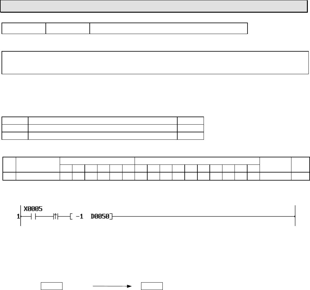
6F3B0253
Basic Hardware and Function 155
7. Instructions
FUN 045 -1 Decrement
Expression
Input −[ -1 A ]− Output
Function
When the input is ON, the data of A is decreased by 1 and stored in A.
Execution condition
Input Operation Output
OFF No execution OFF
ON Execution ON
Operand
Name Device Register Constant Index
X Y R S T. C. XWYWRWSW T C D I J K
AOperation data √√√√√√√√√ √
Example
At the rising edge of X005 changes from OFF to ON, the data of D0050 is decreased by 1 and
stored in D0050.
If the data of D0050 is 1022 before the execution, it will be 1021 after the execution.
D0050 D0050
1022 - 1 1021
Note
• There is no limit value for this instruction. When the data of operand A is -32768 before the
execution, it will be 32767 after the execution.
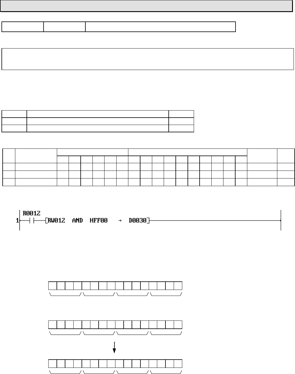
6F3B0253
156 T1-16S User’s Manual
7. Instructions
FUN 048 AND AND
Expression
Input −[ A AND B → C ]− Output
Function
When the input is ON, this instruction finds logical AND of A and B, and stores the result in C.
Execution condition
Input Operation Output
OFF No execution OFF
ON Execution ON
Operand
Name Device Register Constant Index
X Y R S T. C. XWYWRWSW T C D I J K
ASource √√√√√√√√√√ √ √
BSource √√√√√√√√√√ √ √
CAND √√√√√√√√√ √
Example
When R012 is ON, logical AND operation is executed for the data of RW12 and the constant
data HFF00, and the result is stored in D0030.
If the data of RW12 is H3456, the result H3400 is stored in D0030.
FEDCBA9876543210
RW12 0011010001010110
3456
AND
Constant 1111111100000000
FF00
D0030 0011010000000000
3400

6F3B0253
Basic Hardware and Function 157
7. Instructions
FUN 050 OR OR
Expression
Input −[ A OR B → C ]− Output
Function
When the input is ON, this instruction finds logical OR of A and B, and stores the result in C.
Execution condition
Input Operation Output
OFF No execution OFF
ON Execution ON
Operand
Name Device Register Constant Index
X Y R S T. C. XWYWRWSW T C D I J K
ASource √√√√√√√√√√ √ √
Bsource √√√√√√√√√√ √ √
COR √√√√√√√√√ √
Example
When R012 is ON, logical OR operation is executed for the data of RW13 and RW20, and the
result is stored in D0031.
If the data of RW13 is H5678 and RW20 is H4321, the result H5779 is stored in D0031.
FEDCBA9876543210
RW13 0101011001111000
5678
OR
RW20 0100001100100001
4321
D0031 0101011101111001
5779
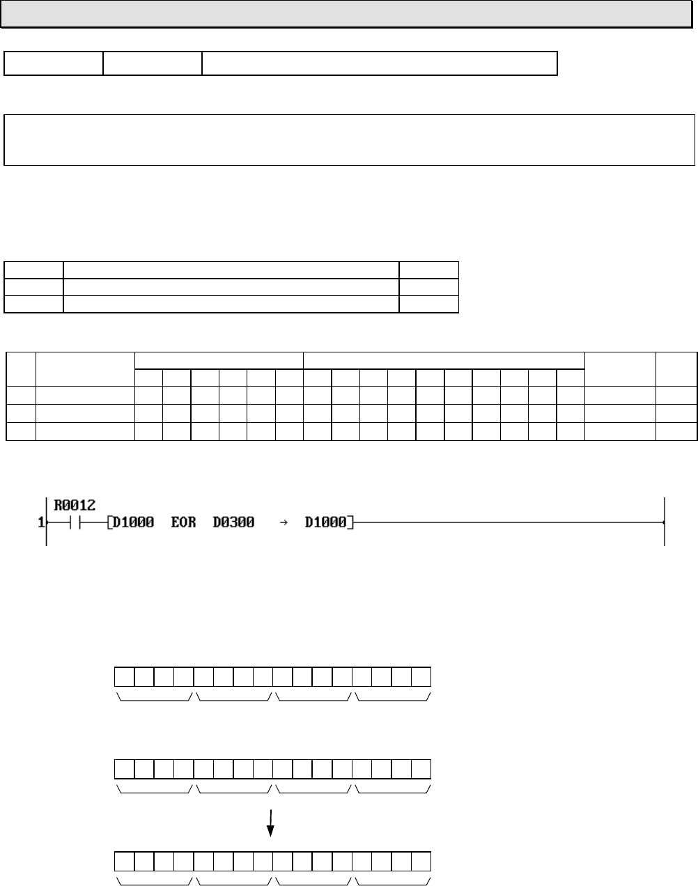
6F3B0253
158 T1-16S User’s Manual
7. Instructions
FUN 052 EOR Exclusive OR
Expression
Input −[ A EOR B → C ]− Output
Function
When the input is ON, this instruction finds exclusive OR of A and B, and stores the result in C.
Execution condition
Input Operation Output
OFF No execution OFF
ON Execution ON
Operand
Name Device Register Constant Index
X Y R S T. C. XWYWRWSW T C D I J K
ASource √√√√√√√√√√ √ √
Bsource √√√√√√√√√√ √ √
CExclusive OR √√√√√√√√√ √
Example
When R012 is ON, exclusive OR operation is executed for the data of D1000 and D0300, and
the result is stored in D1000.
If the data of D1000 is H5678 and D0300 is H4321, the result H1559 is stored in D1000.
FEDCBA9876543210
D1000 0101011001111000
5678
Exclusive OR
D0300 0100001100100001
4321
D1000 0001010101011001
1559
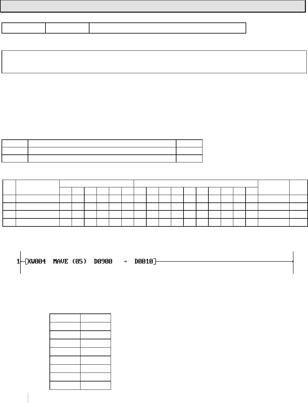
6F3B0253
Basic Hardware and Function 159
7. Instructions
FUN 056 MAVE Moving average
Expression
Input −[ A MAVE (n) B → C ]− Output
Function
When the input is ON, this instruction calculates the average value of the latest n scan’s register A
data, and stores it in C. The allowable range of n is 1 to 64.
This instruction is useful for filtering the analog input signal.
The latest n scan’s data of A are stored in n registers starting with B, and C+1 are used as pointer.
Execution condition
Input Operation Output
OFF No execution OFF
ON Execution ON
Operand
Name Device Register Constant Index
X Y R S T. C. XWYWRWSW T C D I J K
AInput data √√√√√√√√√√ √
nData size 1 - 64
BStart of table √√√√√√
COutput data √√√√√√√√
Example
The latest 5 scan’s data of XW04 is stored in D0900 to D0904 (5 registers), and the average
value of them is calculated and stored in D0010.
D0011 is used as internal work data.
XW04 D0010
1st scan 1000 200 = (1000) / 5
2nd scan 1005 401 = (1000 + 1005) / 5
3rd scan 1009 603 = (1000 + 1005 + 1009) / 5
4th scan 1012 805 = (1000 + 1005 + 1009 + 1012) / 5
5th scan 1007 1006 = (1000 + 1005 + 1009 + 1012 + 1007) / 5
6th scan 1004 1007 = (1005 + 1009 + 1012 + 1007 + 1004) / 5
7th scan 998 1006 = (1009 + 1012 + 1007 + 1004 + 998) / 5
8th scan 994 1003 = (1012 + 1007 + 1004 + 998 + 994) / 5
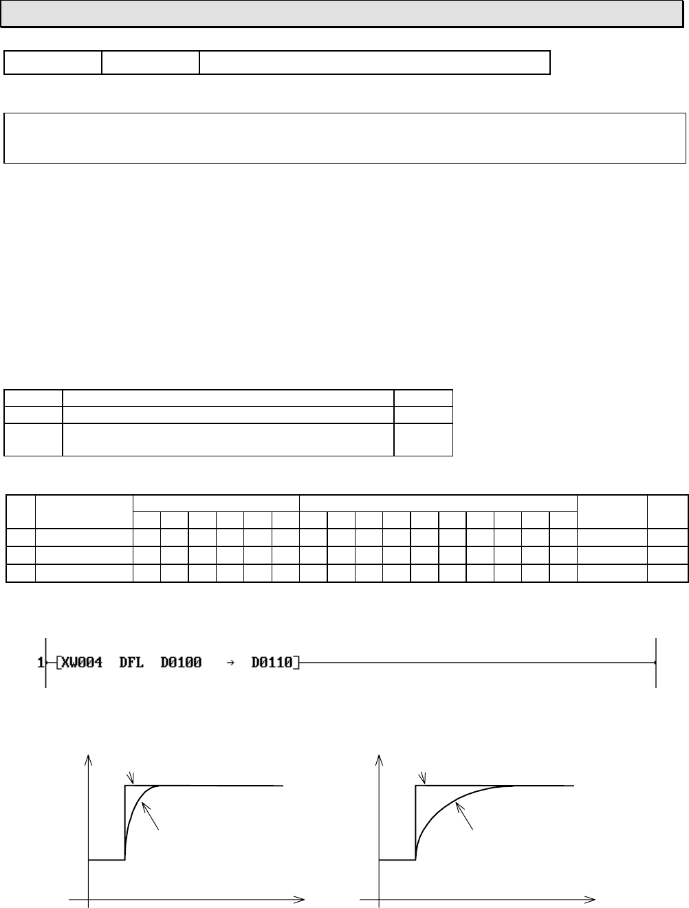
6F3B0253
160 T1-16S User’s Manual
7. Instructions
FUN 061 DFL Digital Filter
Expression
Input −[ A DFL B → C ]− Output
Function
When the input is ON, this instruction calculates the following formula to perform digital filtering for
input data A by filter constant by B, and stores the result in C.
()
yFLxFLy
nnn
=− × + × −
11
Here; xn is input data specified by A
FL is filter constant, 1/10000 of data specified by B (data range: 0 to 9999)
yn is output data to be stored in C
yn-1 is output data at last scan
This instruction is useful for filtering the analog input signal. C+1 is used for internal work data.
Execution condition
Input Operation Output
OFF No execution OFF
ON Execution (FL is limited within the range of 0 to
9999) ON
Operand
Name Device Register Constant Index
X Y R S T. C. XWYWRWSW T C D I J K
AInput data √√√√√√√√√√ √
BFilter constant √√√√√√√
COutput data √√√√√√
Example
The filtered data of XW04 is stored in D0110. (D0111 is used for internal work data)
XW04
D0110
Time
XW04
D0110
Time
When D0100 value is largeWhen D0100 value is small
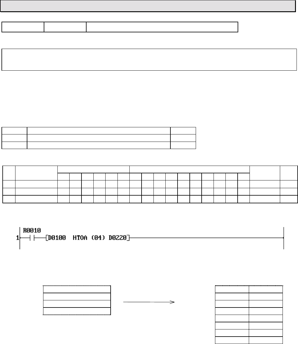
6F3B0253
Basic Hardware and Function 161
7. Instructions
FUN 062 HTOA Hex to ASCII conversion
Expression
Input −[ A HTOA (n) B ]− Output
Function
When the input is ON, the hexadecimal data of n registers starting with A is converted into ASCII
characters and stored in B and after. The uppermost digit of source A is stored in lower byte of
destination B, and followed in this order. The allowable range of n is 1 to 32.
Execution condition
Input Operation Output
OFF No execution OFF
ON Execution ON
Operand
Name Device Register Constant Index
X Y R S T. C. XWYWRWSW T C D I J K
ASource √√√√√√√√√√ √
nData size 1 - 32
BDestination √√√√√√
Example
When R010 is ON, 4 words data of D0100 to D0103 are converted into ASCII characters, and
stored in 8 words registers starting with D0200.
F0 F870
D0100 H0123 D0220 “1” (H31) “0” (H30)
D0101 H4567 Converted D0221 “3” (H33) “2” (H32)
D0102 H89AB D0222 “5” (H35) “4” (H34)
D0103 HCDEF D0223 “7” (H37) “6” (H36)
D0224 “9” (H39) “8” (H38)
D0225 “B” (H42) “A” (H41)
D0226 “D” (H44) “C” (H43)
D0227 “F” (H46) “E” (H45)
Note
• If index register (I, J or K) is used for the operand A, only n = 1 is allowed. Otherwise,
boundary error will occur.
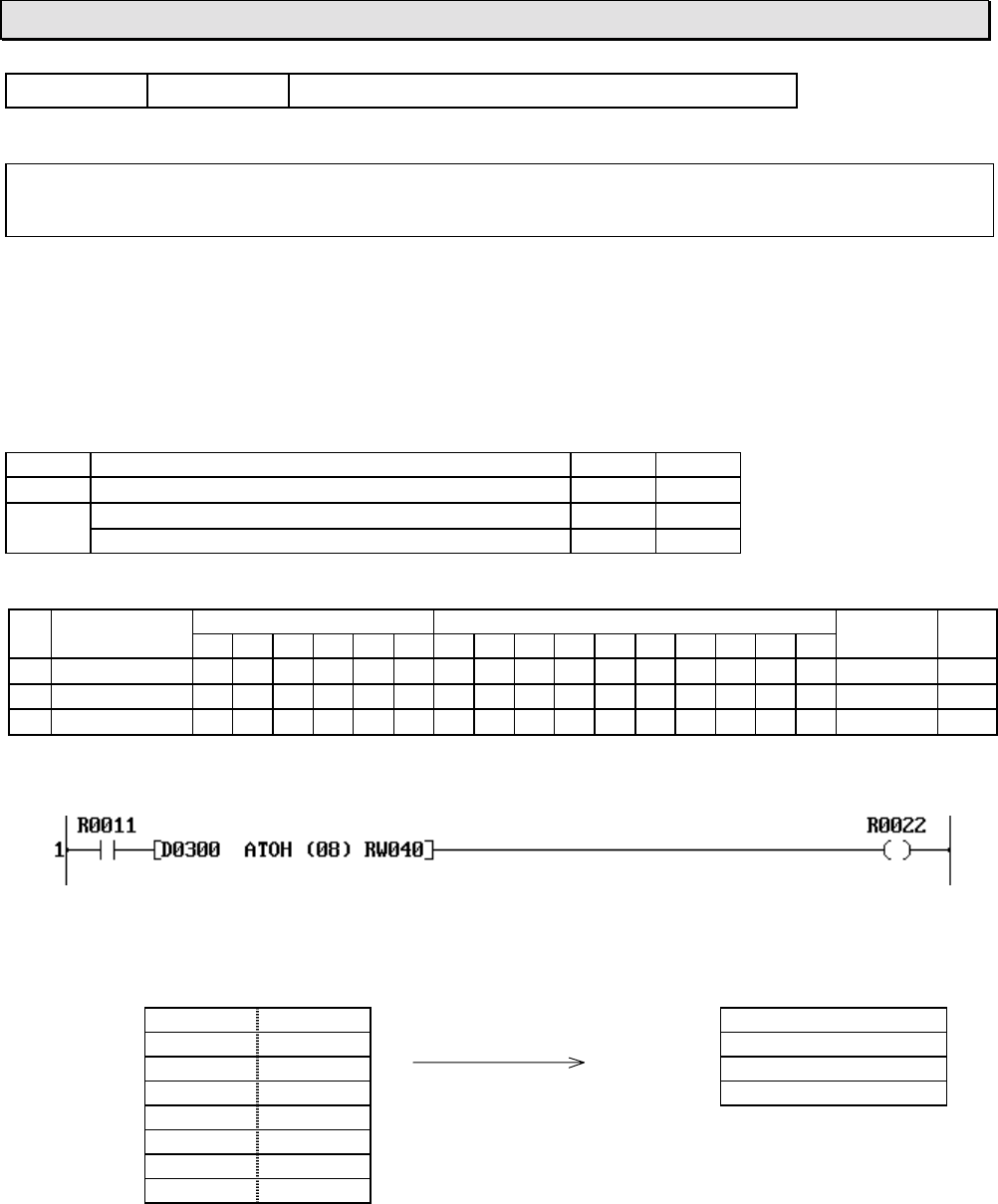
6F3B0253
162 T1-16S User’s Manual
7. Instructions
FUN 063 ATOH ASCII to Hex conversion
Expression
Input −[ A ATOH (n) B ]− Output
Function
When the input is ON, the ASCII characters stored in n registers starting with A is converted into
hexadecimal data and stored in B and after. The lower byte of source A is stored as uppermost
digit of destination B, and followed in this order. The allowable ASCII character in the source table
is “0” (H30) to “9” (H39) and “A” (H41) to “F” (H46). The allowable range of n is 1 to 64.
Execution condition
Input Operation Output ERF
OFF No execution OFF −
ON Normal execution ON −
Conversion data error (no execution) OFF Set
Operand
Name Device Register Constant Index
X Y R S T. C. XWYWRWSW T C D I J K
ASource √√√√√√√√√√ √
nData size 1 - 64
BDestination √√√√√√
Example
When R011 is ON, the ASCII characters stored in 8 words of D0300 to D0307 are converted
into hexadecimal data, and stored in 4 words registers starting with RW040.
F870 F 0
D0300 “1” (H31) “0” (H30) RW040 H0123
D0301 “3” (H33) “2” (H32) Converted RW041 H4567
D0302 “5” (H35) “4” (H34) RW042 H89AB
D0303 “7” (H37) “6” (H36) RW043 HCDEF
D0304 “9” (H39) “8” (H38)
D0305 “B” (H42) “A” (H41)
D0306 “D” (H44) “C” (H43)
D0307 “F” (H46) “E” (H45)
Note
• If index register (I, J or K) is used for the operand A, only n = 1 is allowed.
• If n is odd number, lower 2 digits of the last converted data will not be fixed, Use even for n.
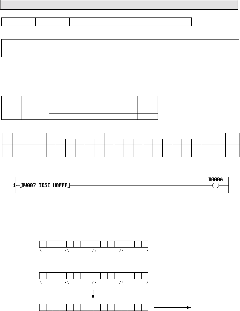
6F3B0253
Basic Hardware and Function 163
7. Instructions
FUN 064 TEST Bit test
Expression
Input −[ A TEST B ]− Output
Function
When the input is ON, this instruction finds logical AND of A and B. Then if the result is not 0, sets
the output to ON.
Execution condition
Input Operation Output
OFF No execution OFF
ON Execution When the result is not 0 ON
When the result is 0 OFF
Operand
Name Device Register Constant Index
X Y R S T. C. XWYWRWSW T C D I J K
ASource √√√√√√√√√√ √ √
BTest data √√√√√√√√√√ √ √
Example
Logical AND operation is executed for the data of RW07 and the constant data H0FFF, and if
the result is not 0, R00A is turned ON. (R00A is turned ON when any device from R070 to
R07B is ON.)
If the data of RW07 is H4008, R00A is turned ON.
FEDCBA9876543210
RW07 0100000000001000
4008
AND
Constant 0000111111111111
0FFF
Result is not 0
Result 0000000000001000 R00A comes ON

6F3B0253
164 T1-16S User’s Manual
7. Instructions
FUN 068 SHR1 1 bit shift right
Expression
Input −[ SHR1 A ]− Output
Function
When the input is ON, the data of register A is shifted 1 bit to the right (LSB direction). 0 is stored in
the left most bit (MSB). The pushed out bit state is stored in the carry flag (CF = S050). After the
operation, if the right most bit (LSB) is ON, the output is turned ON.
Execution condition
Input Operation Output CF
OFF No execution OFF −
ON Execution When LSB = 1 ON Set or reset
When LSB = 0 OFF Set or reset
Operand
Name Device Register Constant Index
X Y R S T. C. XWYWRWSW T C D I J K
AOperation data √√√√√√√√√ √
Example
When X007 is changed from OFF to ON, the data of RW15 is shifted 1 bit to the right.
The figure below shows an operation example.
(MSB) (LSB)
FEDCBA9876543210
RW15 0100001010001010
CF
RW15 0010000101000101 0
(Result)
0 R001 is turned ON

6F3B0253
Basic Hardware and Function 165
7. Instructions
FUN 069 SHL1 1 bit shift left
Expression
Input −[ SHL1 A ]− Output
Function
When the input is ON, the data of register A is shifted 1 bit to the left (MSB direction). 0 is stored in
the right most bit (LSB). The pushed out bit state is stored in the carry flag (CF = S050). After the
operation, if the left most bit (MSB) is ON, the output is turned ON.
Execution condition
Input Operation Output CF
OFF No execution OFF −
ON Execution When MSB = 1 ON Set or reset
When MSB = 0 OFF Set or reset
Operand
Name Device Register Constant Index
X Y R S T. C. XWYWRWSW T C D I J K
AOperation data √√√√√√√√√ √
Example
When X008 is changed from OFF to ON, the data of RW15 is shifted 1 bit to the left.
The figure below shows an operation example.
(MSB) (LSB)
FEDCBA9876543210
1110011100111010
CF
1 1100111001110100
R002 is turned ON 0
RW15
RW15 (Result)
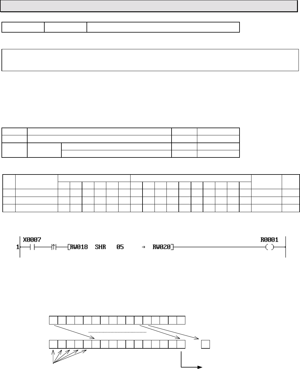
6F3B0253
166 T1-16S User’s Manual
7. Instructions
FUN 070 SHR n bit shift right
Expression
Input −[ A SHR n → B ]− Output
Function
When the input is ON, the data of register A is shifted n bits to the right (LSB direction) including
the carry flag (CF = S050), and stored in B. 0 is stored in upper n bits. After the operation, if the
right most bit (LSB) is ON, the output is turned ON.
Execution condition
Input Operation Output CF
OFF No execution OFF −
ON Execution When LSB = 1 ON Set or reset
When LSB = 0 OFF Set or reset
Operand
Name Device Register Constant Index
X Y R S T. C. XWYWRWSW T C D I J K
ASource √√√√√√√√√√ √ √
nShift bits 1 - 16
BDestination √√√√√√√√√ √
Example
When X007 is changed from OFF to ON, the data of RW18 is shifted 5 bits to the right and the
result is stored in RW20.
The figure below shows an operation example.
(MSB) (LSB)
FEDCBA9876543210
RW18 0100001010011010
CF
RW20 0000001000010100 1
(Result)
0 R001 is turned OFF
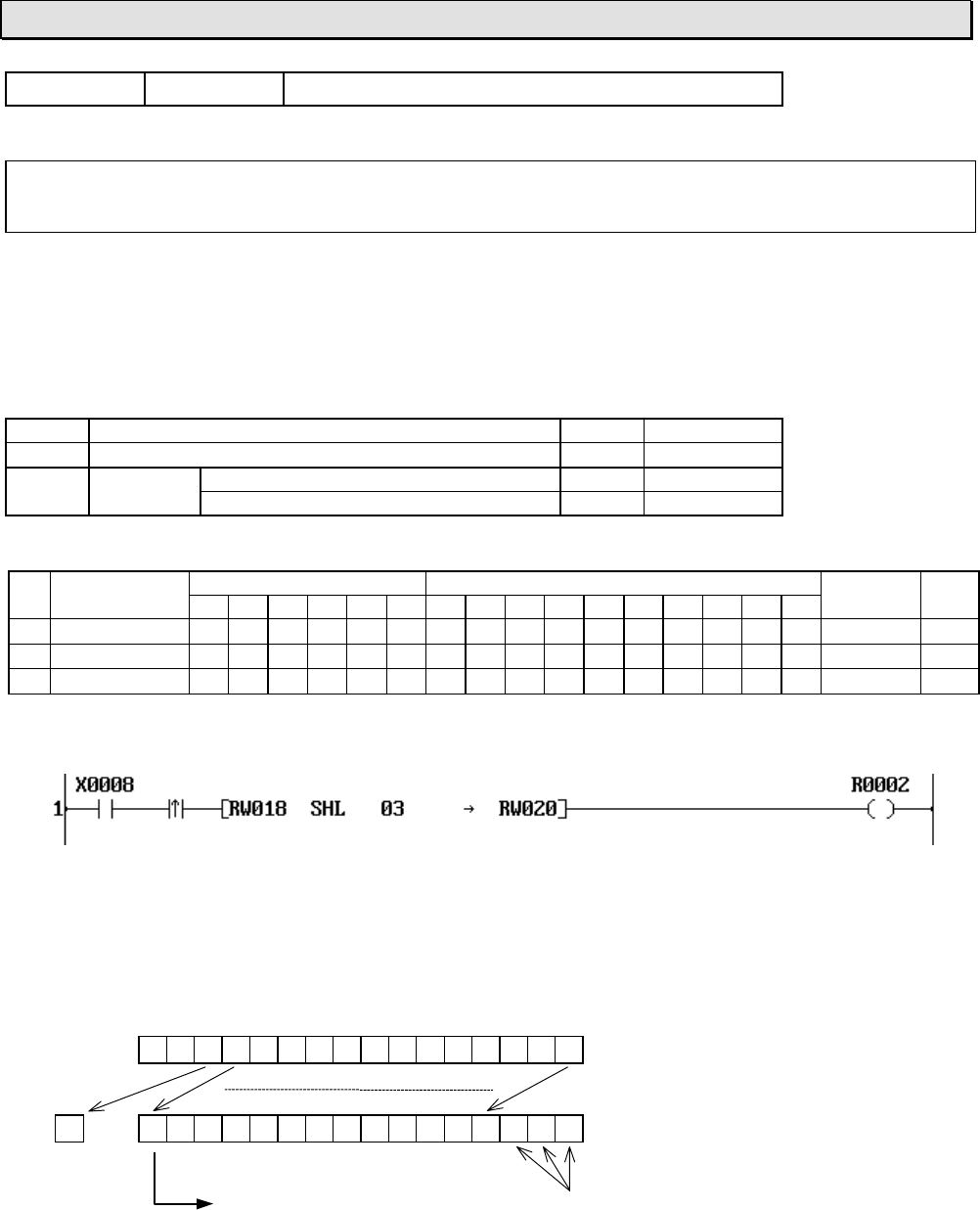
6F3B0253
Basic Hardware and Function 167
7. Instructions
FUN 071 SHL n bit shift left
Expression
Input −[ A SHL n → B ]− Output
Function
When the input is ON, the data of register A is shifted n bits to the left (MSB direction) including the
carry flag (CF = S050), and stored in B. 0 is stored in lower n bits. After the operation, if the left
most bit (MSB) is ON, the output is turned ON.
Execution condition
Input Operation Output CF
OFF No execution OFF −
ON Execution When MSB = 1 ON Set or reset
When MSB = 0 OFF Set or reset
Operand
Name Device Register Constant Index
X Y R S T. C. XWYWRWSW T C D I J K
ASource √√√√√√√√√√ √ √
nShift bits 1 - 16
BDestination √√√√√√√√√ √
Example
When X008 is changed from OFF to ON, the data of RW18 is shifted 3 bits to the left and the
result is stored in RW20.
The figure below shows an operation example.
(MSB) (LSB)
FEDCBA9876543210
1010011100111010
CF
1 0011100111010000
R002 is turned OFF 0
RW18
RW20 (Result)
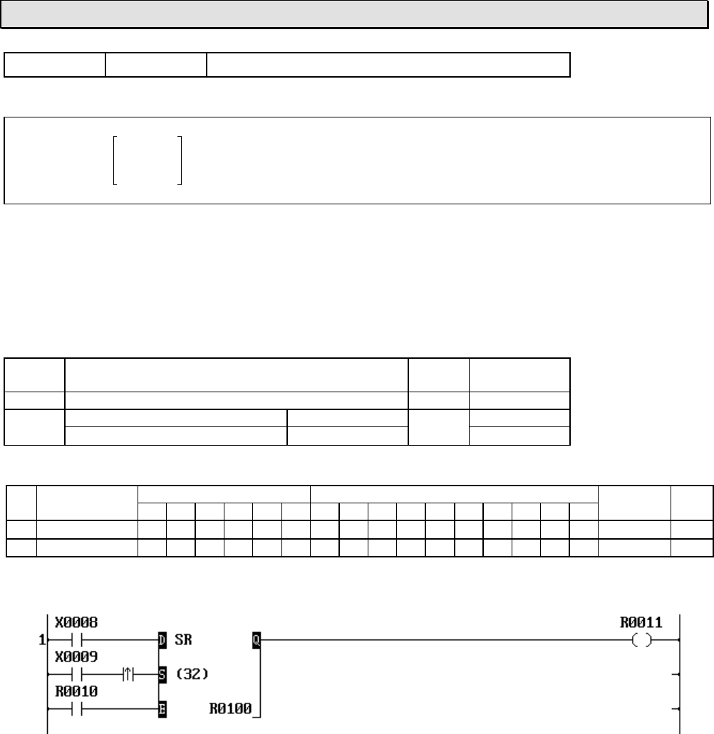
6F3B0253
168 T1-16S User’s Manual
7. Instructions
FUN 074 SR Shift register
Expression
Data input − D SR Q − Output
Shift input − S (n)
Enable input − E A
Function
While the enable input is ON, this instruction shifts the data of the bit table, size n starting with A,
1 bit to the left (upper address direction) when the shift input is ON. The state of the data input is
stored in A. The pushed out bit state is stored in the carry flag (CF = S050).
When the enable input is OFF, all bits in the table and the carry flag are reset to OFF.
Execution condition
Enable
input Operation Output CF
OFF Resets all bits in the bit table OFF Reset
ON When the shift input is ON Shift execution Last bit Set or reset
When the shift input is OFF No execution state −
Operand
Name Device Register Constant Index
X Y R S T. C. XWYWRWSW T C D I J K
ALeading device √√√
nDevice size 1 - 64
Example
32 devices starting with R100 (R100 to R11F) is specified as a shift register.
When R010 is OFF, the data of the shift register is reset to 0. (R100 to R11F are reset to OFF)
The carry flag (CF = S050) is also reset to OFF.
While R010 is ON, the data of the shift register is shifted 1 bit to the upper address direction
when X009 is changed from OFF to ON. At the same time, the state of X008 is stored in the
leading bit (R100).
The output (R011) indicates the state of the last bit (R11F).
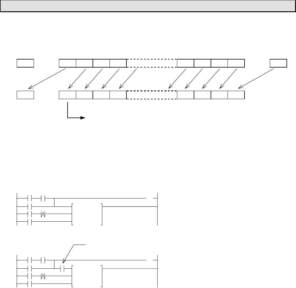
6F3B0253
Basic Hardware and Function 169
7. Instructions
The figure below shows an operation example. (When X009 is changed from OFF to ON)
CF R11F R11E R11D R11C R103 R102 R101 R100 X008
1001 0011 0
1 001 0110
R011 is turned OFF
Note
• When the shift input is ON, the shift operation is performed every scan. Use a transitional
contact for the shift input to detect the state changing.
• For the data input and the shift input, direct linking to a connecting point is not allowed. In this
case, insert a dummy contact (always ON special device = S04F, etc.) just before the input.
( )
D SR QNot allowed
S (n)
E A
Dummy contact
( )
D SR QAllowed
S (n)
E A
Shift result
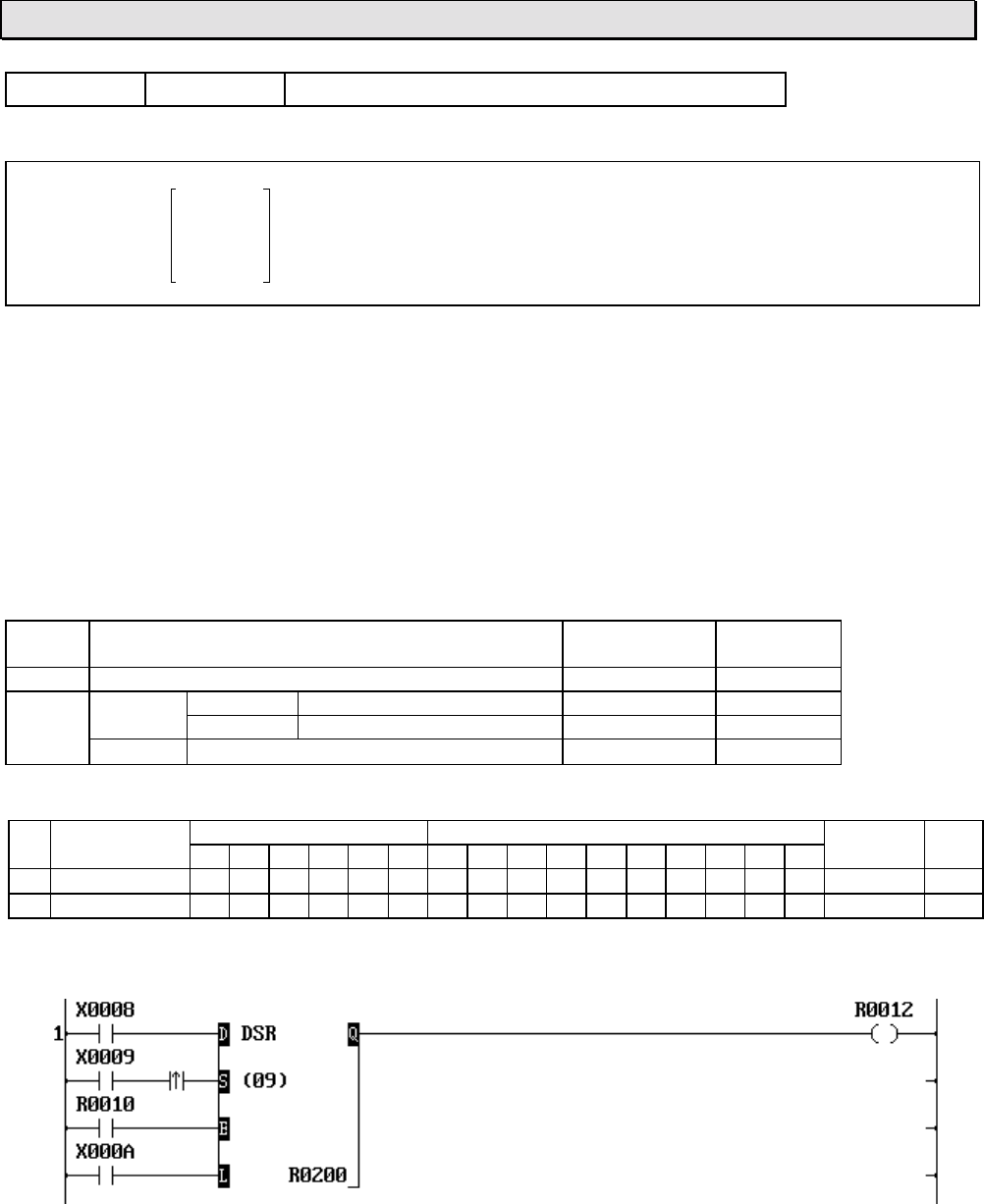
6F3B0253
170 T1-16S User’s Manual
7. Instructions
FUN 075 DSR Bi-directional shift register
Expression
Data input − D DSR Q − Output
Shift input − S (n)
Enable input − E
Direction input − L A
Function
While the enable input (E) is ON, this instruction shifts the data of the bit table, size n starting with
A, 1 bit when the shift input (S) is ON. The shift direction is determined by the state of the direction
input (L).
When L is OFF, the direction is right (lower address direction).
When L is ON, the direction is left (upper address direction).
The state of the data input (D) is stored in the highest bit if right shift, and stored in the lowest bit A
if left shift. The pushed out bit state is stored in the carry flag (CF = S050).
When the enable input (E) is OFF, all bits in the table and the carry flag are reset to OFF.
Execution condition
Enable
input Operation Output CF
OFF Resets all bits in the bit table OFF Reset
ON S = ON L = ON Shift left execution Highest bit state Set or reset
L = OFF Shift right execution Lowest bit state Set or reset
S = OFF No execution Highest bit state −
Operand
Name Device Register Constant Index
X Y R S T. C. XWYWRWSW T C D I J K
ALeading device √√√
nDevice size 1 - 64
Example
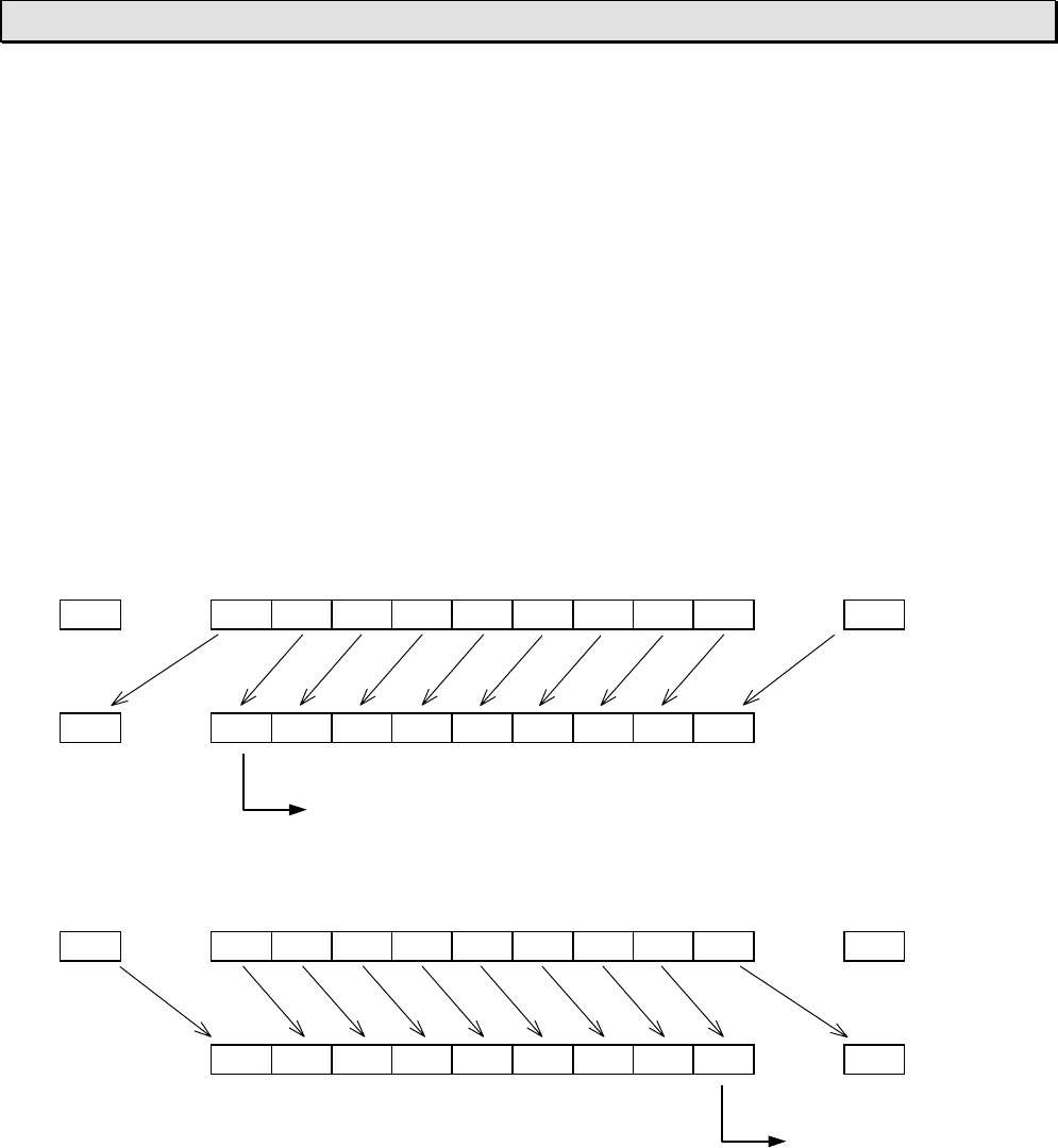
6F3B0253
Basic Hardware and Function 171
7. Instructions
9 devices starting with R200 (R200 to R208) is specified as a shift register.
When R010 is OFF, the data of the shift register is reset to 0. (R200 to R208 are reset to OFF)
The carry flag (CF = S050) is also reset to OFF.
While R010 is ON the following operation is enabled.
• When X00A is ON (shift left), the data of the shift register is shifted 1 bit to the upper
address direction when X009 is changed from OFF to ON. At the same time, the state of
X008 is stored in the leading bit (R200). The output (R012) indicates the state of the highest
bit (R208).
• When X00A is OFF (shift right), the data of the shift register is shifted 1 bit to the lower
address direction when X009 is changed from OFF to ON. At the same time, the state of
X008 is stored in the highest bit (R208). The output (R012) indicates the state of the lowest
bit (R200).
The figure below shows an operation example.
(When X00A is ON and X009 is changed from OFF to ON)
CF R208 R207 R206 R205 R204 R203 R202 R201 R200 X008
100110011 0
1 001100110
R012 is turned OFF
(When X00A is OFF and X009 is changed from OFF to ON)
X008 R208 R207 R206 R205 R204 R203 R202 R201 R200 CF
1 001100110
100110011 0
R012 is turned ON
Note
• When the shift input is ON, the shift operation is performed every scan. Use a transitional
contact for the shift input to detect the state changing.
• For the data input, the shift input and the enable input, direct linking to a connecting point is not
allowed. In this case, insert a dummy contact (always ON special device = S04F, etc.) just
before the input. Refer to Note of Shift register FUN 074.
Shift result
Shift result
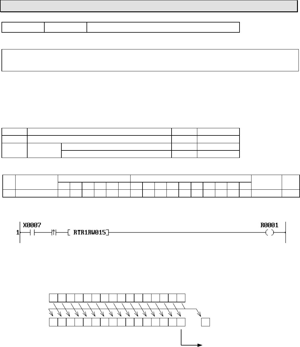
6F3B0253
172 T1-16S User’s Manual
7. Instructions
FUN 078 RTR1 1 bit rotate right
Expression
Input −[ RTR1 A ]− Output
Function
When the input is ON, the data of register A is rotated 1 bit to the right (LSB direction). The pushed
out bit state is stored in the left most bit (MSB) and in the carry flag (CF = S050). After the
operation, if the right most bit (LSB) is ON, the output is turned ON.
Execution condition
Input Operation Output CF
OFF No execution OFF −
ON Execution When LSB = 1 ON Set or reset
When LSB = 0 OFF Set or reset
Operand
Name Device Register Constant Index
X Y R S T. C. XWYWRWSW T C D I J K
AOperation data √√√√√√√√√ √
Example
When X007 is changed from OFF to ON, the data of RW15 is rotated 1 bit to the right.
The figure below shows an operation example.
(MSB) (LSB)
FEDCBA9876543210
RW15 0100001010001010
CF
RW15 0010000101000101 0
(Result)
R001 is turned ON
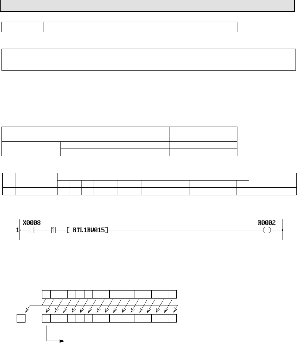
6F3B0253
Basic Hardware and Function 173
7. Instructions
FUN 079 RTL1 1 bit rotate left
Expression
Input −[ RTL1 A ]− Output
Function
When the input is ON, the data of register A is rotated 1 bit to the left (MSB direction). The pushed
out bit state is stored in the right most bit (LSB) and in the carry flag (CF = S050). After the
operation, if the left most bit (MSB) is ON, the output is turned ON.
Execution condition
Input Operation Output CF
OFF No execution OFF −
ON Execution When MSB = 1 ON Set or reset
When MSB = 0 OFF Set or reset
Operand
Name Device Register Constant Index
X Y R S T. C. XWYWRWSW T C D I J K
AOperation data √√√√√√√√√ √
Example
When X008 is changed from OFF to ON, the data of RW15 is rotated 1 bit to the left.
The figure below shows an operation example.
(MSB) (LSB)
FEDCBA9876543210
1110011100111010
CF
1 1100111001110101
R002 is turned ON
RW15
RW15 (Result)
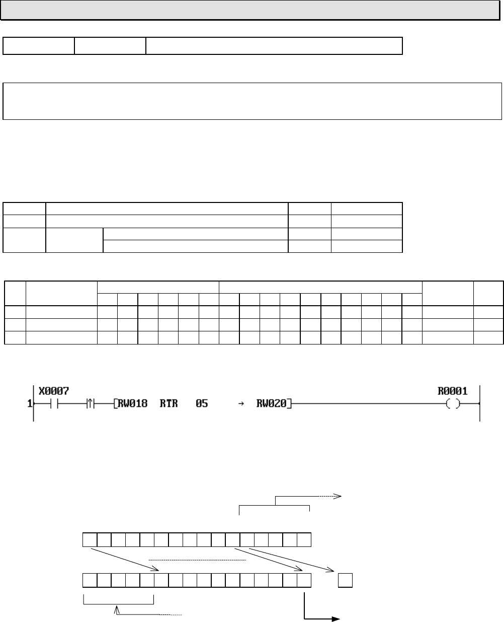
6F3B0253
174 T1-16S User’s Manual
7. Instructions
FUN 080 RTR n bit rotate right
Expression
Input −[ A RTR n → B ]− Output
Function
When the input is ON, the data of register A is rotated n bits to the right (LSB direction), and stored
in B. After the operation, if the right most bit (LSB) is ON, the output is turned ON.
Execution condition
Input Operation Output CF
OFF No execution OFF −
ON Execution When LSB = 1 ON Set or reset
When LSB = 0 OFF Set or reset
Operand
Name Device Register Constant Index
X Y R S T. C. XWYWRWSW T C D I J K
ASource √√√√√√√√√√ √ √
nShift bits 1 - 16
BDestination √√√√√√√√√ √
Example
When X007 is changed from OFF to ON, the data of RW18 is rotated 5 bits to the right and the
result is stored in RW20.
The figure below shows an operation example.
(MSB) (LSB)
FEDCBA9876543210
RW18 0100001010011010
CF
RW20 1101001000010100 1
(Result)
R001 is turned OFF
∗
∗
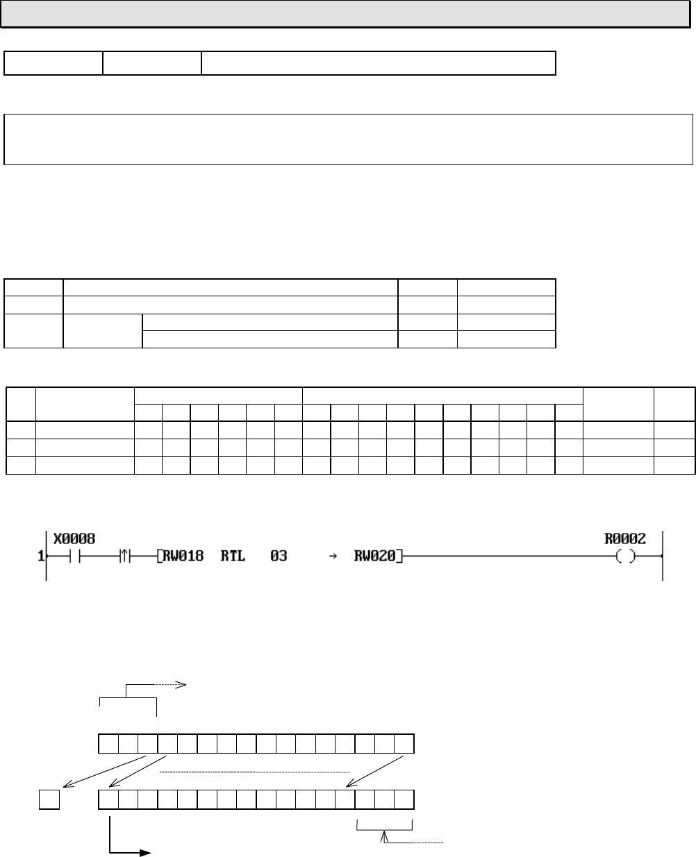
6F3B0253
Basic Hardware and Function 175
7. Instructions
FUN 081 RTL n bit rotate left
Expression
Input −[ A RTL n → B ]− Output
Function
When the input is ON, the data of register A is rotated n bits to the left (MSB direction), and stored
in B. After the operation, if the left most bit (MSB) is ON, the output is turned ON.
Execution condition
Input Operation Output CF
OFF No execution OFF −
ON Execution When MSB = 1 ON Set or reset
When MSB = 0 OFF Set or reset
Operand
Name Device Register Constant Index
X Y R S T. C. XWYWRWSW T C D I J K
ASource √√√√√√√√√√ √ √
nShift bits 1 - 16
BDestination √√√√√√√√√ √
Example
When X008 is changed from OFF to ON, the data of RW18 is rotated 3 bits to the left and the
result is stored in RW20.
The figure below shows an operation example.
(MSB) (LSB)
FEDCBA9876543210
1010011100111010
CF
1 0011100111010101
R002 is turned OFF
RW18
RW20 (Result)
∗
∗
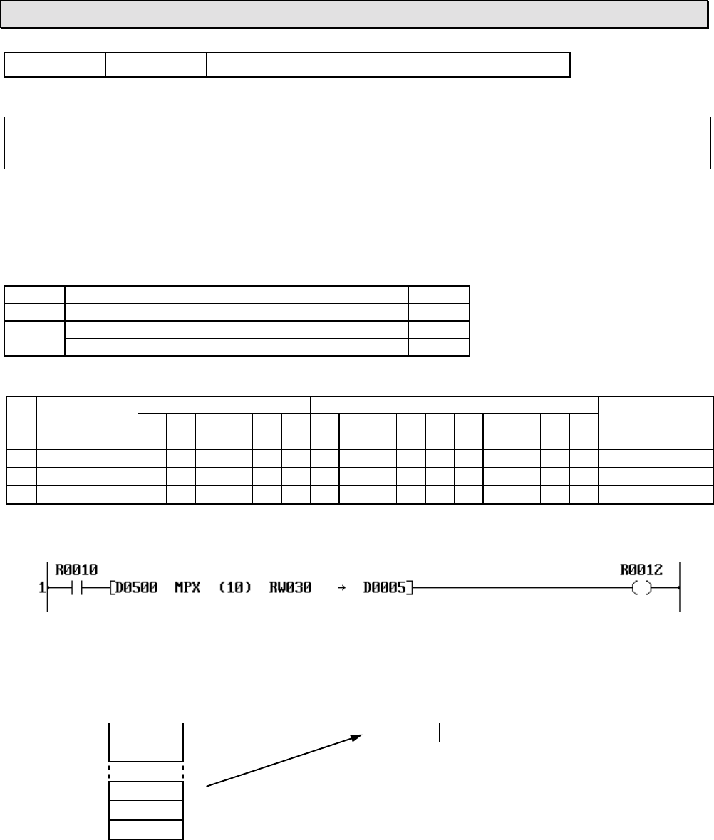
6F3B0253
176 T1-16S User’s Manual
7. Instructions
FUN 090 MPX Multiplexer
Expression
Input −[ A MPX (n) B → C ]− Output
Function
When the input is ON, the data of the register which is designated by B in the table, size n starting
with A, is transferred to C.
Execution condition
Input Operation Output
OFF No execution OFF
ON Normal execution OFF
Pointer over (no execution) ON
Operand
Name Device Register Constant Index
X Y R S T. C. XWYWRWSW T C D I J K
AStart of table √√√√√√√
nTable size 1 - 64
BPointer √√√√√√√√√√ 0 - 63
CDestination √√√√√√√√√
Example
When R010 is ON, the register data which is designated by RW30 is read from the table
D0500 to D0509 (10 registers size), and stored in D0005.
If the data of RW30 is 7, D0507 data is transferred to D0005.
Source table Pointer Destination
D0500 0 D0005 12345
D0501 1
D0507 12345 7
D0508 8
D0509 9
Note
• If the pointer data designates outside the table (10 or more in the above example), the transfer
is not executed and the output comes ON.
• The table must be within the effective range of the register address.
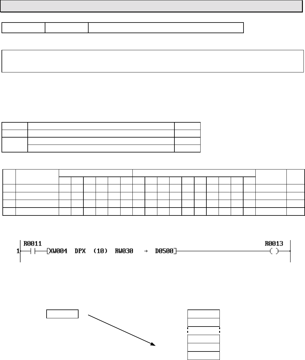
6F3B0253
Basic Hardware and Function 177
7. Instructions
FUN 091 DPX Demultiplexer
Expression
Input −[ A DPX (n) B → C ]− Output
Function
When the input is ON, the data of A is transferred to the register which is designated by B in the
table, size n starting with C.
Execution condition
Input Operation Output
OFF No execution OFF
ON Normal execution OFF
Pointer over (no execution) ON
Operand
Name Device Register Constant Index
X Y R S T. C. XWYWRWSW T C D I J K
ASource √√√√√√√√√√ √
nTable size 1 - 64
BPointer √√√√√√√√√√ 0 - 63
CStart of table √√√√√√
Example
When R011 is ON, the data of XW04 is transferred to the register which is designated by
RW30 in the table D0500 to D0509 (10 registers size).
If the data of RW30 is 8, XW04 data is transferred to D0508.
Source Destination table Pointer
XW04 3210 D0500 0
D0501 1
D0507 7
D0508 3210 8
D0509 9
Note
• If the pointer data designates outside the table (10 or more in the above example), the transfer
is not executed and the output comes ON.
• The table must be within the effective range of the register address.
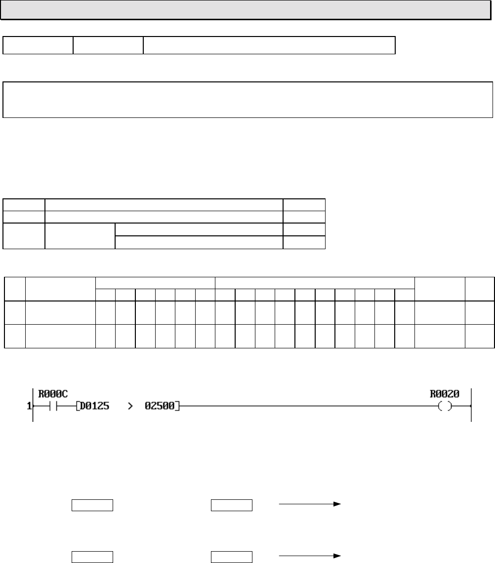
6F3B0253
178 T1-16S User’s Manual
7. Instructions
FUN 096 >Greater than
Expression
Input −[ A > B ]− Output
Function
When the input is ON, the data of A and the data of B are compared, and if A is greater than B, the
output is turned ON.
Execution condition
Input Operation Output
OFF No execution OFF
ON Execution A > BON
A ≤ BOFF
Operand
Name Device Register Constant Index
X Y R S T. C. XWYWRWSW T C D I J K
ACompared
data √√√√√√√√√√ √ √
BReference
data √√√√√√√√√√ √ √
Example
When R00C is ON, the data of D0125 is compared with the constant data 2500, and if the data
of D0125 is greater than 2500, R020 is turned ON.
If the data of D0125 is 3000, the comparison result is true. Consequently, R020 is turned ON.
D0125 3000 >Constant 2500 R020 is ON
If the data of D0125 is -100, the comparison result is false. Consequently, R020 is turned OFF.
D0125 -100 ≤Constant 2500 R020 is OFF
Note
• This instruction deals with the data as signed integer (-32768 to 32767).
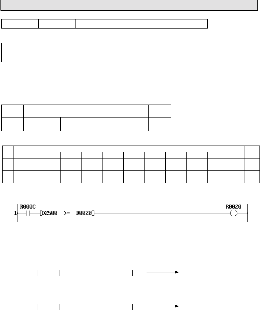
6F3B0253
Basic Hardware and Function 179
7. Instructions
FUN 097 >= Greater than or equal
Expression
Input −[ A >= B ]− Output
Function
When the input is ON, the data of A and the data of B are compared, and if A is greater than or
equal to B, the output is turned ON.
Execution condition
Input Operation Output
OFF No execution OFF
ON Execution A ≥ BON
A < BOFF
Operand
Name Device Register Constant Index
X Y R S T. C. XWYWRWSW T C D I J K
ACompared
data √√√√√√√√√√ √ √
BReference
data √√√√√√√√√√ √ √
Example
When R00C is ON, the data of D0125 is compared with the data of D0020, and if the data of
D0125 is greater than or equal to the data of D0020, R020 is turned ON.
If the data of D0125 is 3000 and that of D0020 is 3000, the comparison result is true.
Consequently, R020 is turned ON.
D0125 3000 ≥D0020 3000 R020 is ON
If the data of D0125 is -1500 and that of D0020 is 0, the comparison result is false.
Consequently, R020 is turned OFF.
D0125 -1500 <D0020 0 R020 is OFF
Note
• This instruction deals with the data as signed integer (-32768 to 32767).

6F3B0253
180 T1-16S User’s Manual
7. Instructions
FUN 098 =Equal
Expression
Input −[ A = B ]− Output
Function
When the input is ON, the data of A and the data of B are compared, and if A is equal to B, the
output is turned ON.
Execution condition
Input Operation Output
OFF No execution OFF
ON Execution A = BON
A ≠ BOFF
Operand
Name Device Register Constant Index
X Y R S T. C. XWYWRWSW T C D I J K
ACompared
data √√√√√√√√√√ √ √
BReference
data √√√√√√√√√√ √ √
Example
When R00C is ON, the data of D0125 is compared with the data of D0030, and if the data of
D0125 is equal to the data of D0030, R020 is turned ON.
If the data of D0125 is 3000 and that of D0020 is 3000, the comparison result is true.
Consequently, R020 is turned ON.
D0125 3000 =D0030 3000 R020 is ON
If the data of D0125 is -1500 and that of D0020 is 0, the comparison result is false.
Consequently, R020 is turned OFF.
D0125 -1500 ≠D0030 0 R020 is OFF
Note
• This instruction deals with the data as signed integer (-32768 to 32767).

6F3B0253
Basic Hardware and Function 181
7. Instructions
FUN 099 <> Not equal
Expression
Input −[ A <> B ]− Output
Function
When the input is ON, the data of A and the data of B are compared, and if A is not equal to B, the
output is turned ON.
Execution condition
Input Operation Output
OFF No execution OFF
ON Execution A ≠ BON
A = BOFF
Operand
Name Device Register Constant Index
X Y R S T. C. XWYWRWSW T C D I J K
ACompared
data √√√√√√√√√√ √ √
BReference
data √√√√√√√√√√ √ √
Example
When R00C is ON, the data of D0125 is compared with the constant data 0, and if the data of
D0125 is not 0, R020 is turned ON.
If the data of D0125 is 10, the comparison result is true. Consequently, R020 is turned ON.
D0125 10 ≠Constant 0 R020 is ON
If the data of D0125 is 0, the comparison result is false. Consequently, R020 is turned OFF.
D0125 0 =Constant 0 R020 is OFF
Note
• This instruction deals with the data as signed integer (-32768 to 32767).

6F3B0253
182 T1-16S User’s Manual
7. Instructions
FUN 100 <Less than
Expression
Input −[ A < B ]− Output
Function
When the input is ON, the data of A and the data of B are compared, and if A is less than B, the
output is turned ON.
Execution condition
Input Operation Output
OFF No execution OFF
ON Execution A < BON
A ≥ BOFF
Operand
Name Device Register Constant Index
X Y R S T. C. XWYWRWSW T C D I J K
ACompared
data √√√√√√√√√√ √ √
BReference
data √√√√√√√√√√ √ √
Example
When R00C is ON, the data of D0125 is compared with the data of D0040, and if the data of
D0125 is less than the data of D0040, R020 is turned ON.
If the data of D0125 is 10 and that of D0040 is 15, the comparison result is true. Consequently,
R020 is turned ON.
D0125 10 <D0040 15 R020 is ON
If the data of D0125 is 0 and that of D0040 is -50, the comparison result is false.
Consequently, R020 is turned OFF.
D0125 0 ≥D0040 0 R020 is OFF
Note
• This instruction deals with the data as signed integer (-32768 to 32767).
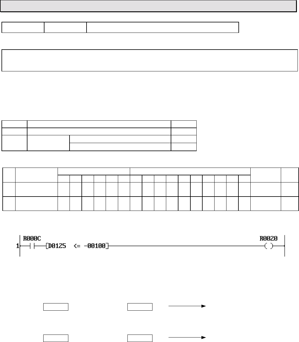
6F3B0253
Basic Hardware and Function 183
7. Instructions
FUN 101 <= Less than or equal
Expression
Input −[ A <= B ]− Output
Function
When the input is ON, the data of A and the data of B are compared, and if A is less than or equal
to B, the output is turned ON.
Execution condition
Input Operation Output
OFF No execution OFF
ON Execution A ≤ BON
A > BOFF
Operand
Name Device Register Constant Index
X Y R S T. C. XWYWRWSW T C D I J K
ACompared
data √√√√√√√√√√ √ √
BReference
data √√√√√√√√√√ √ √
Example
When R00C is ON, the data of D0125 is compared with the constant data -100, and if the data
of D0125 is less than or equal to -100, R020 is turned ON.
If the data of D0125 is -150, the comparison result is true. Consequently, R020 is turned ON.
D0125 -150 <Constant -100 R020 is ON
If the data of D0125 is 0, the comparison result is false. Consequently, R020 is turned OFF.
D0125 0 ≥Constant -100 R020 is OFF
Note
• This instruction deals with the data as signed integer (-32768 to 32767).
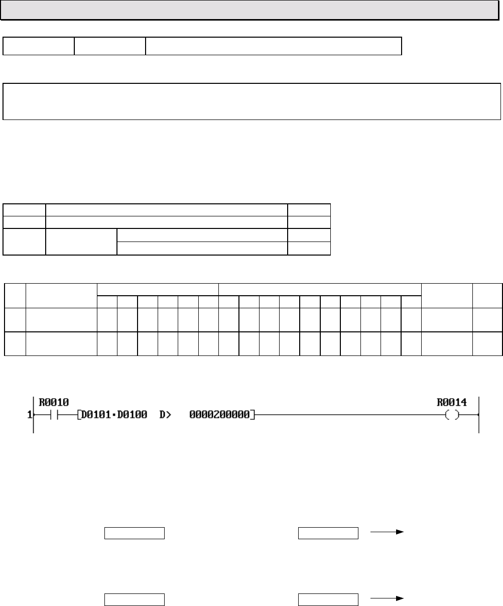
6F3B0253
184 T1-16S User’s Manual
7. Instructions
FUN 102 D>Double-word greater than
Expression
Input −[ A+1⋅A D> B+1⋅B ]− Output
Function
When the input is ON, the double-word data of A+1⋅A and B+1⋅B are compared, and if A+1⋅A is
greater than B+1⋅B, the output is turned ON.
Execution condition
Input Operation Output
OFF No execution OFF
ON Execution A+1⋅A > B+1⋅BON
A+1⋅A ≤ B+1⋅BOFF
Operand
Name Device Register Constant Index
X Y R S T. C. XWYWRWSW T C D I J K
ACompared
data √√√√√√√ √
BReference
data √√√√√√√ √
Example
When R010 is ON, the data of D0101⋅D0100 is compared with the constant data 200000, and
if the data of D0101⋅D0100 is greater than 200000, R014 is turned ON.
If the data of D0101⋅D0100 is 250000, the comparison result is true. Consequently, R014 is
turned ON.
D0101⋅D0100 250000 >Constant 200000 R014 is ON
If the data of D0101⋅D0100 is -100, the comparison result is false. Consequently, R014 is
turned OFF.
D0101⋅D0100 -100 ≤Constant 200000 R014 is OFF
Note
• This instruction deals with the data as double-word integer (-2147483648 to 2147483647).

6F3B0253
Basic Hardware and Function 185
7. Instructions
FUN 103 D>= Double-word greater than or equal
Expression
Input −[ A+1⋅A D>= B+1⋅B ]− Output
Function
When the input is ON, the double-word data of A+1⋅A and B+1⋅B are compared, and if A+1⋅A is
greater than or equal to B+1⋅B, the output is turned ON.
Execution condition
Input Operation Output
OFF No execution OFF
ON Execution A+1⋅A ≥ B+1⋅BON
A+1⋅A < B+1⋅BOFF
Operand
Name Device Register Constant Index
X Y R S T. C. XWYWRWSW T C D I J K
ACompared
data √√√√√√√ √
BReference
data √√√√√√√ √
Example
When R010 is ON, the double-word data of D0101⋅D0100 is compared with the double-word
data of D0251⋅D0250, and if the data of D0101⋅D0100 is greater than or equal to the data of
D0251⋅D0250, R014 is turned ON.
If the data of D0101⋅D0100 is 250000 and D0251⋅D0250 is 200000, R014 is turned ON.
D0101⋅D0100 250000 ≥D0251⋅D0250 200000 R014 is ON
If the data of D0101⋅D0100 is -100 and D0251⋅D0250 is 0, R014 is turned OFF.
D0101⋅D0100 -100 <D0251⋅D0250 0 R014 is OFF
Note
• This instruction deals with the data as double-word integer (-2147483648 to 2147483647).
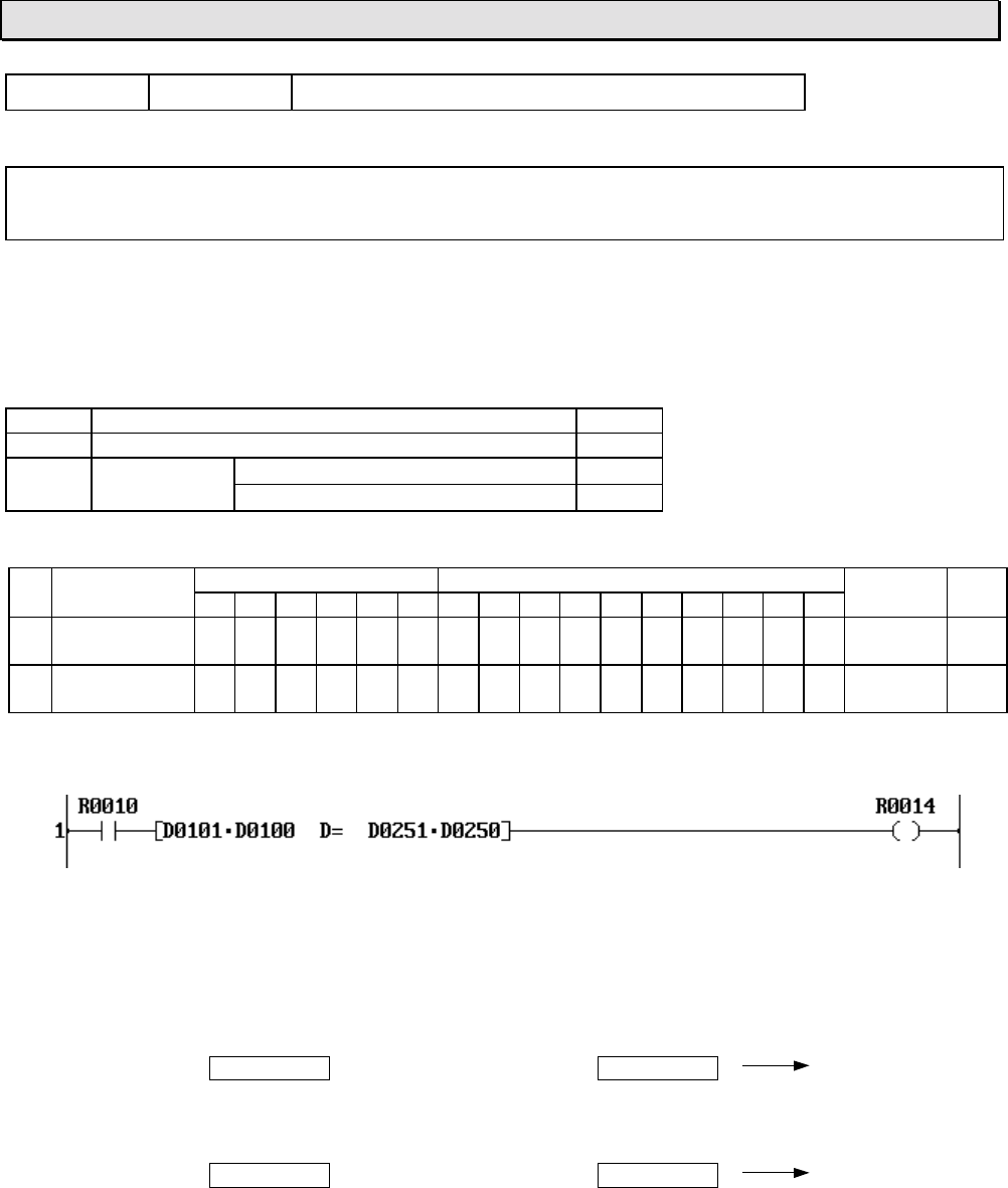
6F3B0253
186 T1-16S User’s Manual
7. Instructions
FUN 104 D=Double-word equal
Expression
Input −[ A+1⋅A D= B+1⋅B ]− Output
Function
When the input is ON, the double-word data of A+1⋅A and B+1⋅B are compared, and if A+1⋅A is
equal to B+1⋅B, the output is turned ON.
Execution condition
Input Operation Output
OFF No execution OFF
ON Execution A+1⋅A = B+1⋅BON
A+1⋅A ≠ B+1⋅BOFF
Operand
Name Device Register Constant Index
X Y R S T. C. XWYWRWSW T C D I J K
ACompared
data √√√√√√√ √
BReference
data √√√√√√√ √
Example
When R010 is ON, the double-word data of D0101⋅D0100 is compared with the double-word
data of D0251⋅D0250, and if the data of D0101⋅D0100 is equal to the data of D0251⋅D0250,
R014 is turned ON.
If the data of D0101⋅D0100 is 250000 and D0251⋅D0250 is 250000, R014 is turned ON.
D0101⋅D0100 250000 =D0251⋅D0250 250000 R014 is ON
If the data of D0101⋅D0100 is -100 and D0251⋅D0250 is 0, R014 is turned OFF.
D0101⋅D0100 -100 ≠D0251⋅D0250 0 R014 is OFF
Note
• This instruction deals with the data as double-word integer (-2147483648 to 2147483647).
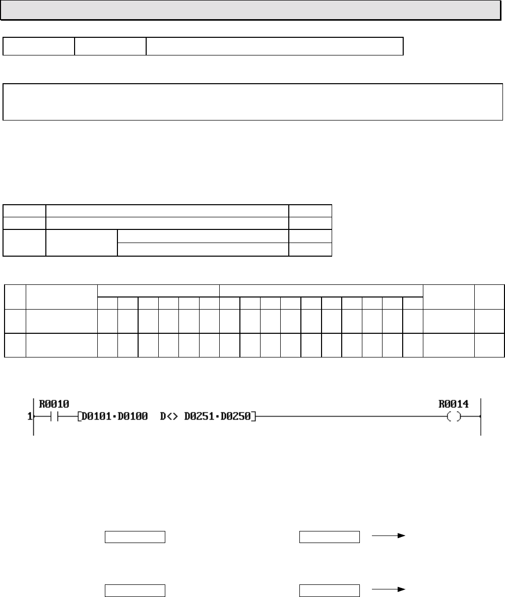
6F3B0253
Basic Hardware and Function 187
7. Instructions
FUN 105 D<> Double-word not equal
Expression
Input −[ A+1⋅A D<> B+1⋅B ]− Output
Function
When the input is ON, the double-word data of A+1⋅A and B+1⋅B are compared, and if A+1⋅A is not
equal to B+1⋅B, the output is turned ON.
Execution condition
Input Operation Output
OFF No execution OFF
ON Execution A+1⋅A ≠ B+1⋅BON
A+1⋅A = B+1⋅BOFF
Operand
Name Device Register Constant Index
X Y R S T. C. XWYWRWSW T C D I J K
ACompared
data √√√√√√√ √
BReference
data √√√√√√√ √
Example
When R010 is ON, the double-word data of D0101⋅D0100 is compared with the double-word
data of D0251⋅D0250, and if the data of D0101⋅D0100 is not equal to the data of
D0251⋅D0250, R014 is turned ON.
If the data of D0101⋅D0100 is 250000 and D0251⋅D0250 is 200000, R014 is turned ON.
D0101⋅D0100 250000 ≠D0251⋅D0250 250000 R014 is ON
If the data of D0101⋅D0100 is -100 and D0251⋅D0250 is -100, R014 is turned OFF.
D0101⋅D0100 -100 =D0251⋅D0250 -100 R014 is OFF
Note
• This instruction deals with the data as double-word integer (-2147483648 to 2147483647).
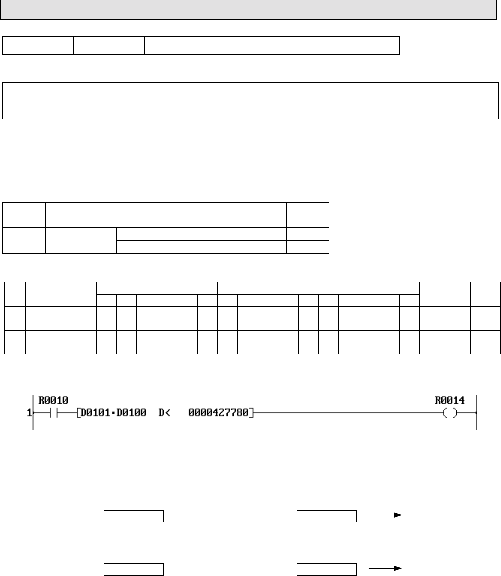
6F3B0253
188 T1-16S User’s Manual
7. Instructions
FUN 106 D<Double-word less than
Expression
Input −[ A+1⋅A D< B+1⋅B ]− Output
Function
When the input is ON, the double-word data of A+1⋅A and B+1⋅B are compared, and if A+1⋅A is
less than B+1⋅B, the output is turned ON.
Execution condition
Input Operation Output
OFF No execution OFF
ON Execution A+1⋅A < B+1⋅BON
A+1⋅A ≥ B+1⋅BOFF
Operand
Name Device Register Constant Index
X Y R S T. C. XWYWRWSW T C D I J K
ACompared
data √√√√√√√ √
BReference
data √√√√√√√ √
Example
When R010 is ON, the data of D0101⋅D0100 is compared with the constant data 427780, and
if the data of D0101⋅D0100 is less than 427780, R014 is turned ON.
If the data of D0101⋅D0100 is 250000, R014 is turned ON.
D0101⋅D0100 250000 <Constant 427780 R014 is ON
If the data of D0101⋅D0100 is 430000, R014 is turned OFF.
D0101⋅D0100 430000 ≥Constant 427780 R014 is OFF
Note
• This instruction deals with the data as double-word integer (-2147483648 to 2147483647).
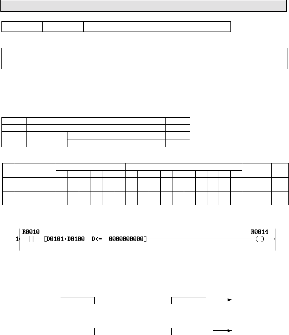
6F3B0253
Basic Hardware and Function 189
7. Instructions
FUN 107 D<= Double-word less than or equal
Expression
Input −[ A+1⋅A D<= B+1⋅B ]− Output
Function
When the input is ON, the double-word data of A+1⋅A and B+1⋅B are compared, and if A+1⋅A is
less than or equal to B+1⋅B, the output is turned ON.
Execution condition
Input Operation Output
OFF No execution OFF
ON Execution A+1⋅A ≤ B+1⋅BON
A+1⋅A > B+1⋅BOFF
Operand
Name Device Register Constant Index
X Y R S T. C. XWYWRWSW T C D I J K
ACompared
data √√√√√√√ √
BReference
data √√√√√√√ √
Example
When R010 is ON, the data of D0101⋅D0100 is compared with the constant data 0, and if the
data of D0101⋅D0100 is less than or equal to 0, R014 is turned ON.
If the data of D0101⋅D0100 is -1, R014 is turned ON.
D0101⋅D0100 -1 ≤Constant 0 R014 is ON
If the data of D0101⋅D0100 is 10000, R014 is turned OFF.
D0101⋅D0100 10000 >Constant 0 R014 is OFF
Note
• This instruction deals with the data as double-word integer (-2147483648 to 2147483647).

6F3B0253
190 T1-16S User’s Manual
7. Instructions
FUN 108 U>Unsigned greater than
Expression
Input −[ A U> B ]− Output
Function
When the input is ON, the data of A and the data of B are compared, and if A is greater than B, the
output is turned ON.
Execution condition
Input Operation Output
OFF No execution OFF
ON Execution A > BON
A ≤ BOFF
Operand
Name Device Register Constant Index
X Y R S T. C. XWYWRWSW T C D I J K
ACompared
data √√√√√√√√√√ √ √
BReference
data √√√√√√√√√√ √ √
Example
When R00C is ON, the data of D0125 is compared with the constant data 40000, and if the
data of D0125 is greater than 40000, R020 is turned ON.
If the data of D0125 is 52000, the comparison result is true. Consequently, R020 is turned ON.
D0125 52000 >Constant 40000 R020 is ON
If the data of D0125 is 21000, the comparison result is false. Consequently, R020 is turned
OFF.
D0125 21000 ≤Constant 40000 R020 is OFF
Note
• This instruction deals with the data as unsigned integer (0 to 65535).
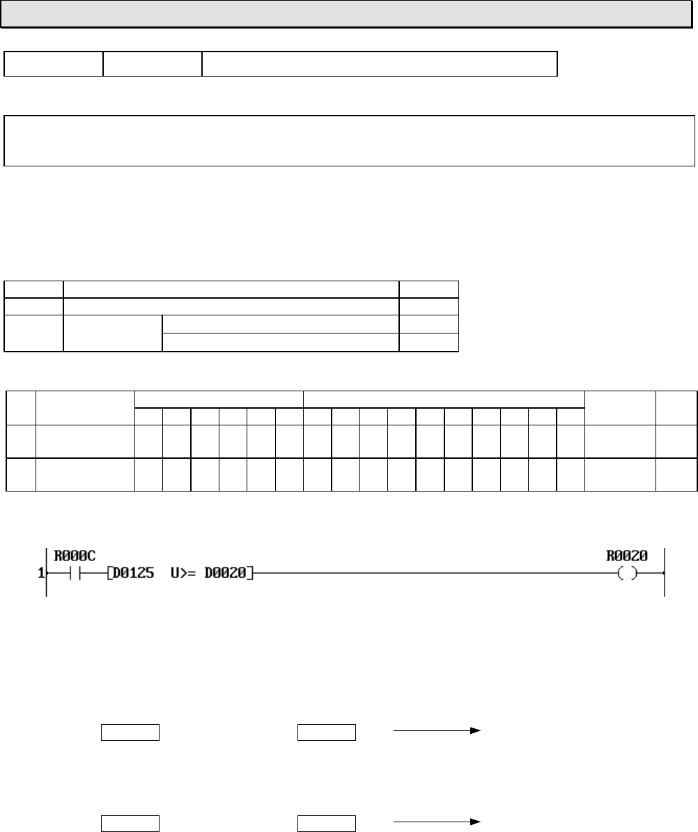
6F3B0253
Basic Hardware and Function 191
7. Instructions
FUN 109 U>= Unsigned greater than or equal
Expression
Input −[ A >= B ]− Output
Function
When the input is ON, the data of A and the data of B are compared, and if A is greater than or
equal to B, the output is turned ON.
Execution condition
Input Operation Output
OFF No execution OFF
ON Execution A ≥ BON
A < BOFF
Operand
Name Device Register Constant Index
X Y R S T. C. XWYWRWSW T C D I J K
ACompared
data √√√√√√√√√√ √ √
BReference
data √√√√√√√√√√ √ √
Example
When R00C is ON, the data of D0125 is compared with the data of D0020, and if the data of
D0125 is greater than or equal to the data of D0020, R020 is turned ON.
If the data of D0125 is 40000 and that of D0020 is 40000, the comparison result is true.
Consequently, R020 is turned ON.
D0125 40000 ≥D0020 40000 R020 is ON
If the data of D0125 is 15000 and that of D0020 is 20000, the comparison result is false.
Consequently, R020 is turned OFF.
D0125 15000 <D0020 20000 R020 is OFF
Note
• This instruction deals with the data as unsigned integer (0 to 65535).
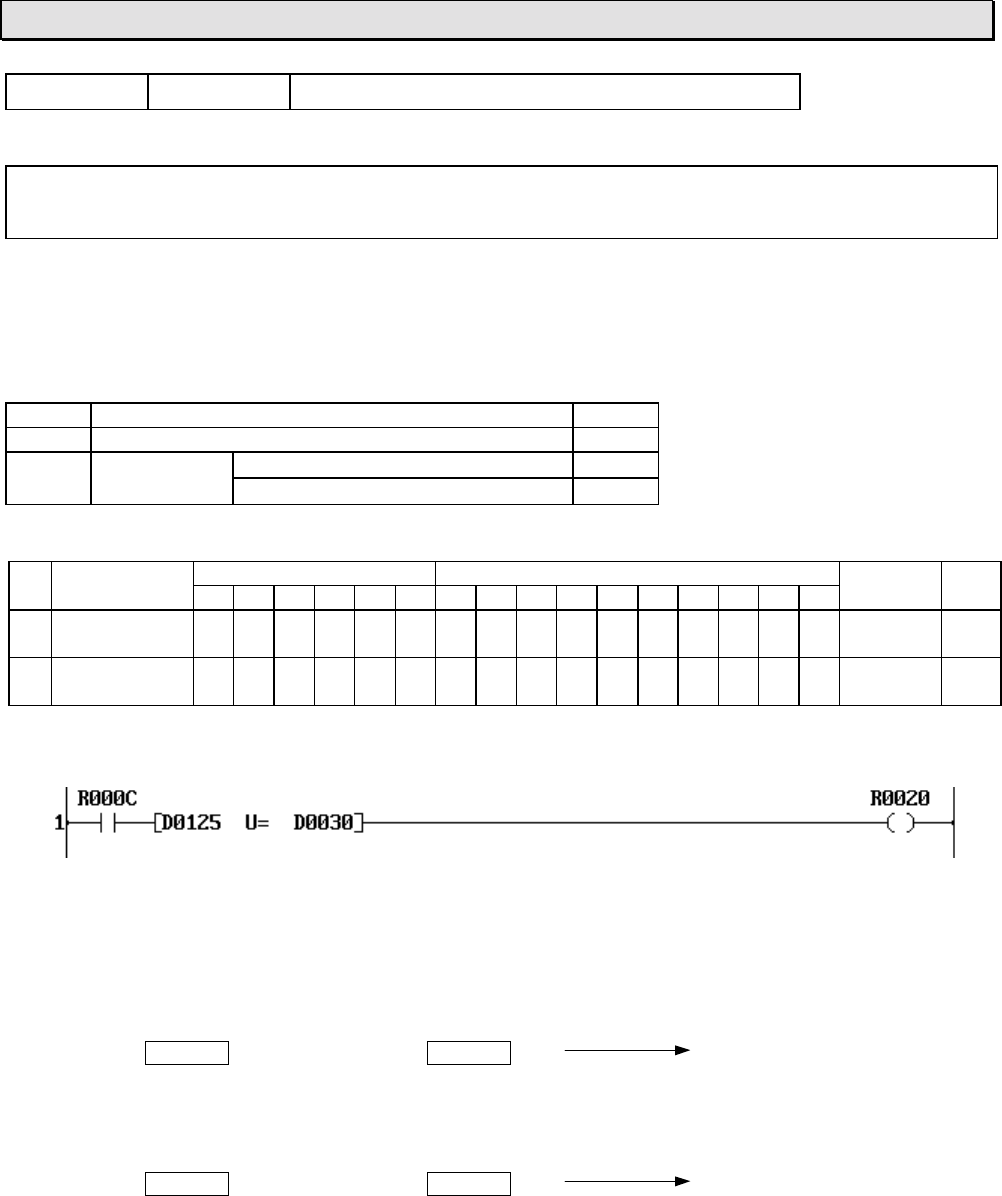
6F3B0253
192 T1-16S User’s Manual
7. Instructions
FUN 110 U=Unsigned equal
Expression
Input −[ A U= B ]− Output
Function
When the input is ON, the data of A and the data of B are compared, and if A is equal to B, the
output is turned ON.
Execution condition
Input Operation Output
OFF No execution OFF
ON Execution A = BON
A ≠ BOFF
Operand
Name Device Register Constant Index
X Y R S T. C. XWYWRWSW T C D I J K
ACompared
data √√√√√√√√√√ √ √
BReference
data √√√√√√√√√√ √ √
Example
When R00C is ON, the data of D0125 is compared with the data of D0030, and if the data of
D0125 is equal to the data of D0030, R020 is turned ON.
If the data of D0125 is 35000 and that of D0020 is 35000, the comparison result is true.
Consequently, R020 is turned ON.
D0125 35000 =D0030 35000 R020 is ON
If the data of D0125 is 1500 and that of D0020 is 4000, the comparison result is false.
Consequently, R020 is turned OFF.
D0125 1500 ≠D0030 4000 R020 is OFF
Note
• This instruction deals with the data as unsigned integer (0 to 65535).
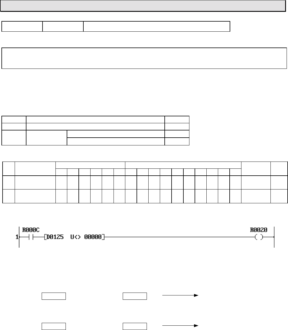
6F3B0253
Basic Hardware and Function 193
7. Instructions
FUN 111 U<> Unsigned not equal
Expression
Input −[ A U<> B ]− Output
Function
When the input is ON, the data of A and the data of B are compared, and if A is not equal to B, the
output is turned ON.
Execution condition
Input Operation Output
OFF No execution OFF
ON Execution A ≠ BON
A = BOFF
Operand
Name Device Register Constant Index
X Y R S T. C. XWYWRWSW T C D I J K
ACompared
data √√√√√√√√√√ √ √
BReference
data √√√√√√√√√√ √ √
Example
When R00C is ON, the data of D0125 is compared with the constant data 0, and if the data of
D0125 is not 0, R020 is turned ON.
If the data of D0125 is 41000, the comparison result is true. Consequently, R020 is turned ON.
D0125 41000 ≠Constant 0 R020 is ON
If the data of D0125 is 0, the comparison result is false. Consequently, R020 is turned OFF.
D0125 0 =Constant 0 R020 is OFF
Note
• This instruction deals with the data as unsigned integer (0 to 65535).

6F3B0253
194 T1-16S User’s Manual
7. Instructions
FUN 112 U<Unsigned less than
Expression
Input −[ A U< B ]− Output
Function
When the input is ON, the data of A and the data of B are compared, and if A is less than B, the
output is turned ON.
Execution condition
Input Operation Output
OFF No execution OFF
ON Execution A < BON
A ≥ BOFF
Operand
Name Device Register Constant Index
X Y R S T. C. XWYWRWSW T C D I J K
ACompared
data √√√√√√√√√√ √ √
BReference
data √√√√√√√√√√ √ √
Example
When R00C is ON, the data of D0125 is compared with the data of D0040, and if the data of
D0125 is less than the data of D0040, R020 is turned ON.
If the data of D0125 is 43000 and that of D0040 is 45000, the comparison result is true.
Consequently, R020 is turned ON.
D0125 43000 <D0040 45000 R020 is ON
If the data of D0125 is 50000 and that of D0040 is 50000, the comparison result is false.
Consequently, R020 is turned OFF.
D0125 50000 ≥D0040 50000 R020 is OFF
Note
• This instruction deals with the data as unsigned integer (0 to 65535).
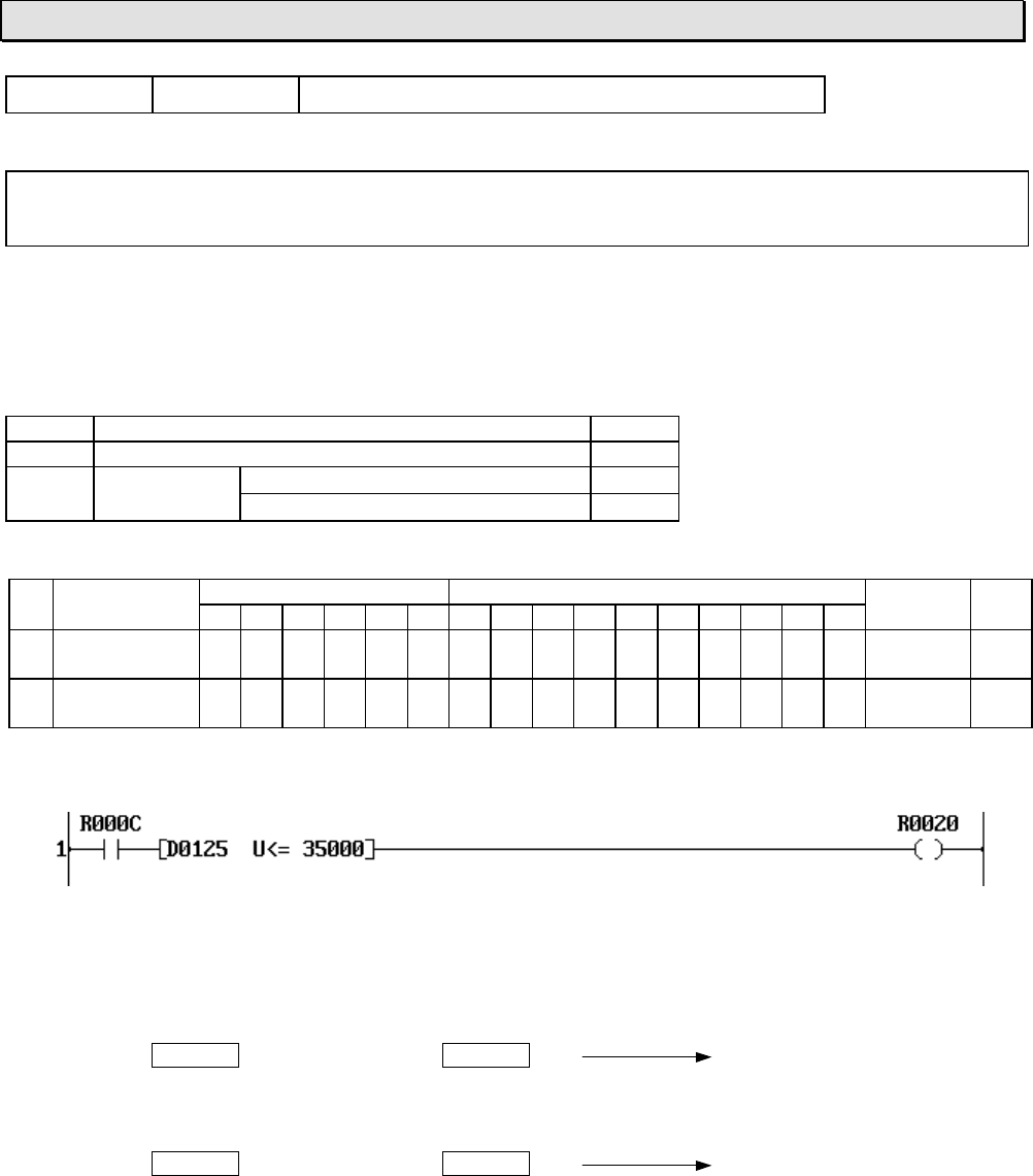
6F3B0253
Basic Hardware and Function 195
7. Instructions
FUN 113 U<= Unsigned less than or equal
Expression
Input −[ A U<= B ]− Output
Function
When the input is ON, the data of A and the data of B are compared, and if A is less than or equal
to B, the output is turned ON.
Execution condition
Input Operation Output
OFF No execution OFF
ON Execution A ≤ BON
A > BOFF
Operand
Name Device Register Constant Index
X Y R S T. C. XWYWRWSW T C D I J K
ACompared
data √√√√√√√√√√ √ √
BReference
data √√√√√√√√√√ √ √
Example
When R00C is ON, the data of D0125 is compared with the constant data 35000, and if the
data of D0125 is less than or equal to 35000, R020 is turned ON.
If the data of D0125 is 35000, the comparison result is true. Consequently, R020 is turned ON.
D0125 35000 ≤Constant 35000 R020 is ON
If the data of D0125 is 0, the comparison result is false. Consequently, R020 is turned OFF.
D0125 38000 >Constant 35000 R020 is OFF
Note
• This instruction deals with the data as unsigned integer (0 to 65535).
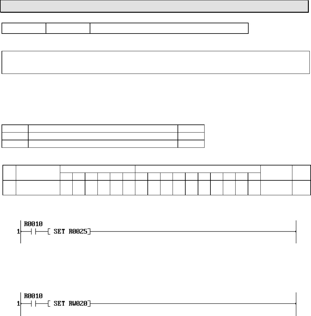
6F3B0253
196 T1-16S User’s Manual
7. Instructions
FUN 114 SET Device/register set
Expression
Input −[ SET A ]− Output
Function
When the input is ON, the device A is set to ON if A is a device, or the data HFFFF is stored in the
register A if A is a register.
Execution condition
Input Operation Output
OFF No execution OFF
ON Execution ON
Operand
Name Device Register Constant Index
X Y R S T. C. XWYWRWSW T C D I J K
ADevice or
register √√√ √√√√√√√√√
Example 1 (device set)
When R010 is ON, R025 is set to ON. The state of R025 is remained even if R010 comes
OFF.
Example 2 (register set)
When R010 is ON, the data HFFFF is stored in RW20. (R200 to R20F are set to ON)
The state of RW20 is remained even if R010 comes OFF.
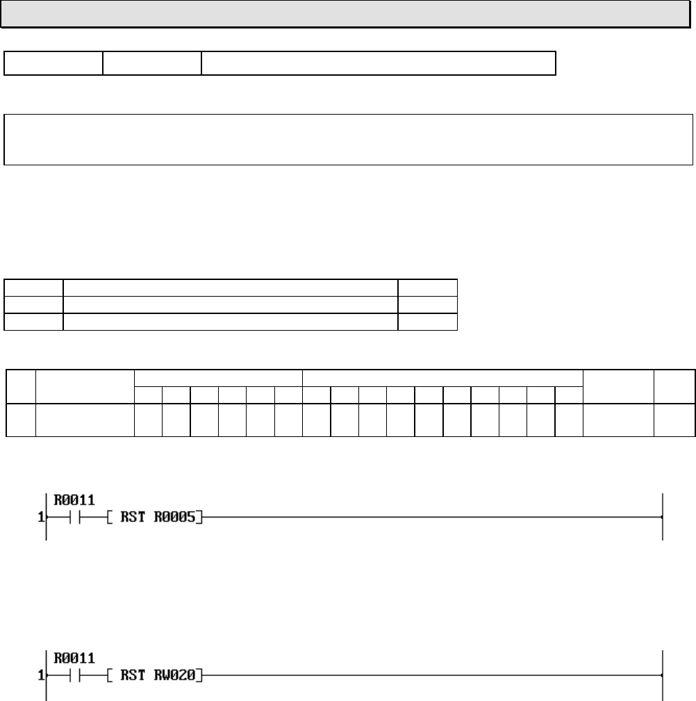
6F3B0253
Basic Hardware and Function 197
7. Instructions
FUN 115 RST Device/register reset
Expression
Input −[ RST A ]− Output
Function
When the input is ON, the device A is reset to OFF if A is a device, or the data 0 is stored in the
register A if A is a register.
Execution condition
Input Operation Output
OFF No execution OFF
ON Execution ON
Operand
Name Device Register Constant Index
X Y R S T. C. XWYWRWSW T C D I J K
ADevice or
register √√√ √√√√√√√√√
Example 1 (device reset)
When R011 is ON, R005 is reset to OFF. The state of R025 is remained even if R011 comes
OFF.
Example 2 (register reset)
When R011 is ON, the data 0 is stored in RW20. (R200 to R20F are reset to OFF)
The state of RW20 is remained even if R011 comes OFF.
6F3B0253
198 T1-16S User’s Manual
7. Instructions
FUN 118 SETC Set carry
Expression
Input −[ SETC ]− Output
Function
When the input is ON, the carry flag (CF = S050) is set to ON.
Execution condition
Input Operation Output CF
OFF No execution OFF −
ON Execution ON Set
Operand
No operand is required.
Example
When R011 is changed from OFF to ON, the carry flag S050 is set to ON.
6F3B0253
Basic Hardware and Function 199
7. Instructions
FUN 119 RSTC Reset carry
Expression
Input −[ RSTC ]− Output
Function
When the input is ON, the carry flag (CF = S050) is reset to OFF.
Execution condition
Input Operation Output CF
OFF No execution OFF −
ON Execution ON Reset
Operand
No operand is required.
Example
When R010 is changed from OFF to ON, the carry flag S050 is reset to OFF.
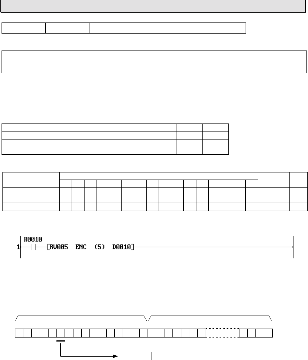
6F3B0253
200 T1-16S User’s Manual
7. Instructions
FUN 120 ENC Encode
Expression
Input −[ A ENC (n) B ]− Output
Function
When the input is ON, this instruction finds the bit position of the most significant ON bit in the bit
table, size 2n bits starting with 0 bit (LSB) of A, and stores it in B.
Execution condition
Input Operation Output ERF
OFF No execution OFF −
ON Normal execution ON −
There is no ON bit (no execution) OFF Set
Operand
Name Device Register Constant Index
X Y R S T. C. XWYWRWSW T C D I J K
AStart of table √√√√√√√
nTable size 1 - 8
BEncode result √√√√√√√√√
Example
25 (=32) bits starting with 0 bit of RW05 (R050 to R06F) are defined as the bit table.
When R010 is ON, the most significant ON (1) bit position in the bit table is searched, and the
position is stored in D0010.
The following figure shows an operation example.
RW06 RW05
313029282726252423222120191817161514131211109 3210
00000100100110000111010 0010
D0010 26
Note
• If there is no ON bit in the bit table, the instruction error flag (ERF = S051) is set to ON.
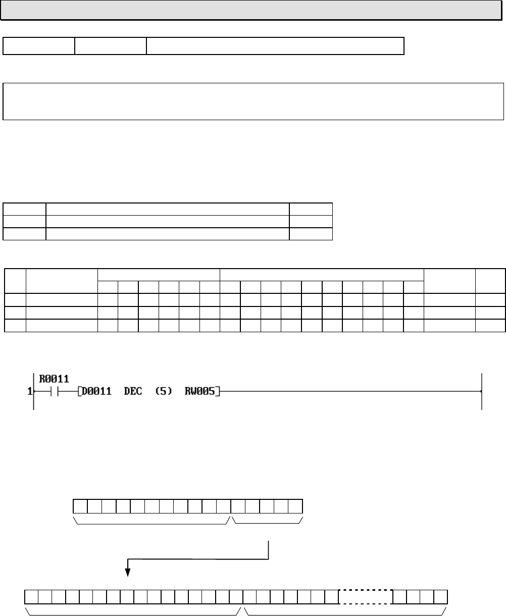
6F3B0253
Basic Hardware and Function 201
7. Instructions
FUN 121 DEC Decode
Expression
Input −[ A DEC (n) B ]− Output
Function
When the input is ON, this instruction sets the bit position which is designated by lower n bits of A
to ON in the bit table, size 2n bits starting with 0 bit (LSB) of B, and resets all other bits to OFF.
Execution condition
Input Operation Output
OFF No execution OFF
ON Execution ON
Operand
Name Device Register Constant Index
X Y R S T. C. XWYWRWSW T C D I J K
ADecode source √√√√√√√√√√
nTable size 1 - 8
BStart of table √√√√√√
Example
25 (=32) bits starting with 0 bit of RW05 (R050 to R06F) are defined as the bit table.
When R011 is ON, the bit position designated by lower 5 bits of D0011 in the bit table is set to
ON, and all other bits in the table are reset to OFF.
The following figure shows an operation example.
FEDCBA9876543210
D0011 1 1000
Ignored H18 (=24)
31 30 29 28 27 26 25 24 23 22 21 20 19 18 17 16 15 14 13 12 11 10 9 3 2 1 0
00000001000000000000000 0000
RW06 RW05
Sets ON
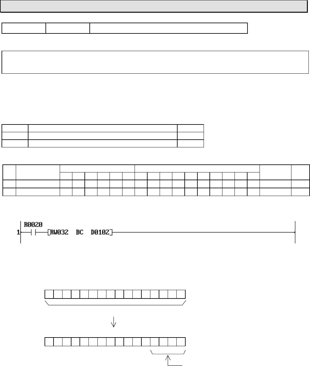
6F3B0253
202 T1-16S User’s Manual
7. Instructions
FUN 122 BC Bit count
Expression
Input −[ A BC B ]− Output
Function
When the input is ON, this instruction counts the number of ON (1) bits of A, and stores the result
in B.
Execution condition
Input Operation Output
OFF No execution OFF
ON Execution ON
Operand
Name Device Register Constant Index
X Y R S T. C. XWYWRWSW T C D I J K
ASource √√√√√√√√√√ √
BCount data √√√√√√
Example
When R020 is ON, the number of ON (1) bits of the register RW032 is counted, and the result
is stored in D0102.
The following figure shows an operation example.
FEDCBA9876543210
RW0320010011101011000
Counts the number of ON (1) bits = 7
FEDCBA9876543210
D0102 0000000000000111
The result data (7) is stored in binary
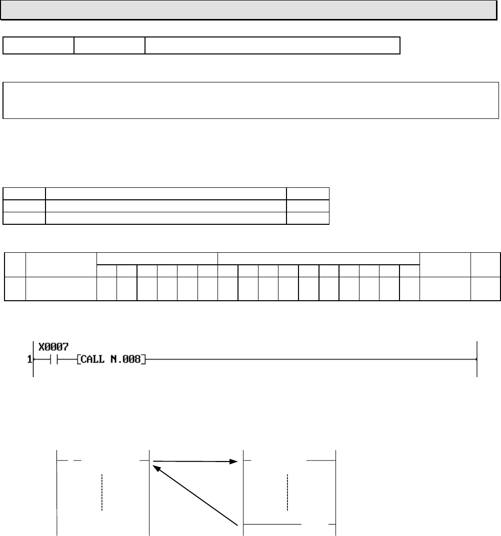
6F3B0253
Basic Hardware and Function 203
7. Instructions
FUN 128 CALL Subroutine call
Expression
Input −[ CALL N. n ]− Output
Function
When the input is ON, this instruction calls the subroutine number n.
Execution condition
Input Operation Output
OFF No execution OFF
ON Execution ON
Operand
Name Device Register Constant Index
X Y R S T. C. XWYWRWSW T C D I J K
nSubroutine
number √ (Note)
Example
When X007 is ON, the subroutine number 8 is called. When the program execution is returned
from the subroutine, the output is turned ON.
Main program Subroutine
| | [ CALL N.008 ] [ SUBR (008)]
[ RET ]
Note
• The possible subroutine number is 0 to 15 (T1) or 0 to 255 (T1S).
• Refer to the SUBR instruction (FUN 137).
• In case of T1, nesting of subroutines is not allowed. That is, the CALL instruction cannot be
used in a subroutine.
• In case of T1S, nesting of subroutines is possible. (up to 3 levels)
• The CALL instruction can be used in an interrupt program. However, it is not allowed that the
same subroutine is called from an interrupt program and from main program.
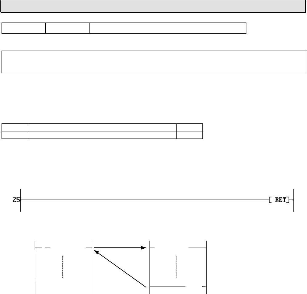
6F3B0253
204 T1-16S User’s Manual
7. Instructions
FUN 129 RET Subroutine return
Expression
−−[ RET ]−
Function
This instruction indicates the end of a subroutine. When program execution is reached this
instruction, it is returned to the original CALL instruction.
Execution condition
Input Operation Output
-Execution -
Operand
No operand is required.
Example
Main program Subroutine
| | [ CALL N.008 ] [ SUBR (008)]
[ RET ]
Note
• Refer to the SUBR instruction (FUN 137).
• The RET instruction can be programmed only in the program type ‘Subroutine’.
• The RET instruction must be connected directly to the left power rail.
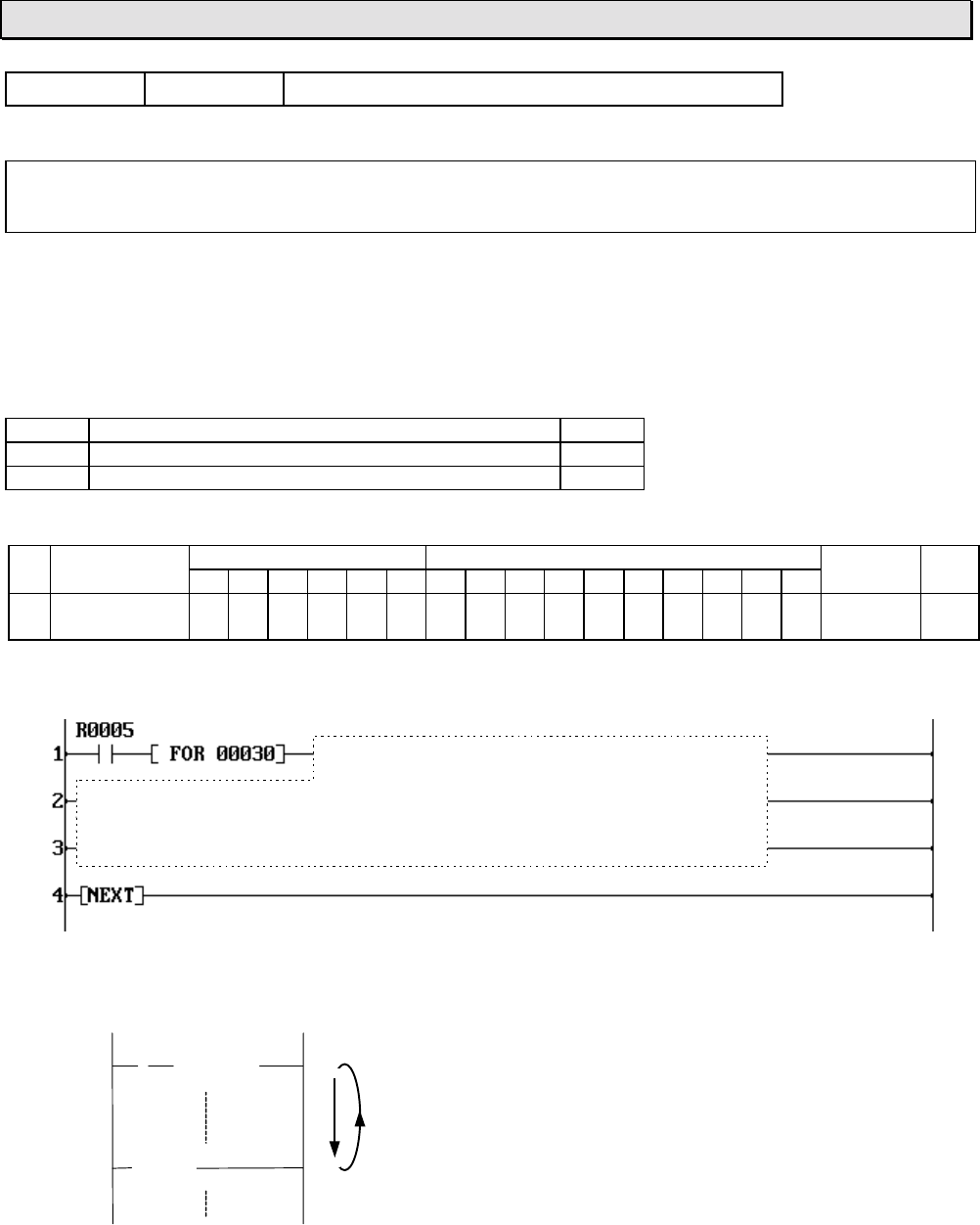
6F3B0253
Basic Hardware and Function 205
7. Instructions
FUN 132 FOR FOR (FOR-NEXT loop)
Expression
Input −[ FOR n ]− Output
Function
When the input is ON, the program segment between FOR and NEXT is executed n times
repeatedly in a scan.
When the input is OFF, the repetition is not performed. (the segment is executed once)
Execution condition
Input Operation Output
OFF No repetition OFF
ON Repetition ON
Operand
Name Device Register Constant Index
X Y R S T. C. XWYWRWSW T C D I J K
nRepetition
times √√√√√√√√√√
1 - 32767
Example
This segment is executed 30 times repeatedly in a scan.
When R005 is ON, the program segment between FOR and NEXT is executed 30 times in a
scan.
R005
| | [ FOR 30 ]
[ NEXT ]
Executed 30 times in a scan when
R005 is ON.
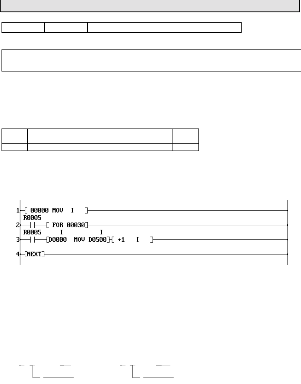
6F3B0253
206 T1-16S User’s Manual
7. Instructions
FUN 133 NEXT NEXT (FOR-NEXT loop)
Expression
Input −[ NEXT ]− Output
Function
This instruction configures a FOR-NEXT loop.
If the input is OFF, The repetition is forcibly broken. and the program execution is moved to the
next instruction.
Execution condition
Input Operation Output
OFF Forcibly breaks the repetition OFF
ON Repetition ON
Operand
No operand is required.
Example
When R005 is ON, the program segment between FOR and NEXT is executed 30 times in a
scan. In the above example, the rung 3 is executed 30 times. As a result, the data of D0000 to
D0029 are transferred to D0500 to D0529. (Block transfer)
Note
• The FOR instruction must be used with a corresponding NEXT instruction one by one.
• Nesting of the FOR-NEXT loop is not allowed. That is, the FOR instruction cannot be used in a
FOR-NEXT loop.
• The FOR and NEXT instructions cannot be programmed on the same rung.
• The following connection is not allowed.
| | [ FOR n ] | | [ NEXT ]
| | | |
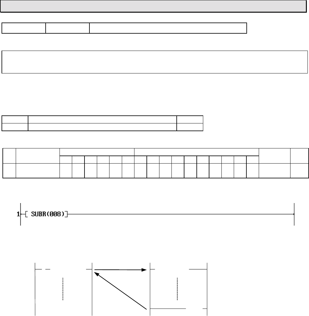
6F3B0253
Basic Hardware and Function 207
7. Instructions
FUN 137 SUBR Subroutine entry
Expression
−[ SUBR (n) ]−−
Function
This instruction indicates the begging of a subroutine.
Execution condition
Input Operation Output
-Execution -
Operand
Name Device Register Constant Index
X Y R S T. C. XWYWRWSW T C D I J K
nSubroutine
number √ (Note)
Example
The begging of the subroutine number 8 is indicated.
Main program Subroutine
| | [ CALL N.008 ] [ SUBR (008)]
[ RET ]
Note
• The possible subroutine number is 0 to 15 (T1) or 0 to 255 (T1S).
• Refer to the CALL instruction (FUN 128) and the RET instruction (FUN 129).
• The SUBR instruction can be programmed only in the program type ‘Subroutine’.
• Nesting of subroutine is not allowed. That is, the CALL instruction cannot be used in a
subroutine.
• No other instruction cannot be placed on the rung of the SUBR instruction.
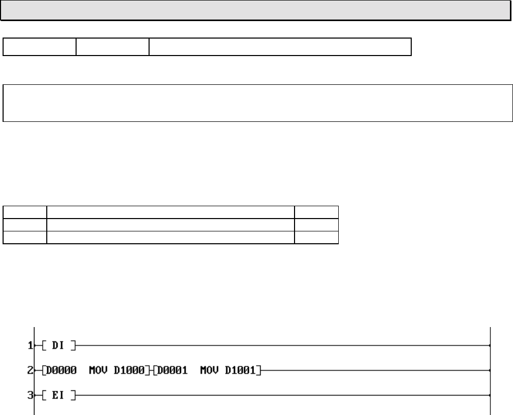
6F3B0253
208 T1-16S User’s Manual
7. Instructions
FUN 140 EI Enable interrupt
Expression
Input −[ EI ]− Output
Function
When the input is ON, this instruction enables the execution of user designated interrupt operation,
i.e. timer interrupt program and I/O interrupt programs.
Execution condition
Input Operation Output
OFF No execution OFF
ON Execution ON
Operand
No operand is required.
Example
In the above example, the DI instruction disables the interrupt. Then the EI instruction enables
the interrupt again. As a result, the rung 2 instructions can be executed without interruption
between each instructions.
Note
• Refer to the DI instruction (FUN 141).
• If an interrupt factor is occurred during the interrupt disabled state, the interrupt is kept waiting
and it will be executed just after the EI instruction is executed.
• The EI instruction can be used only in the main program.
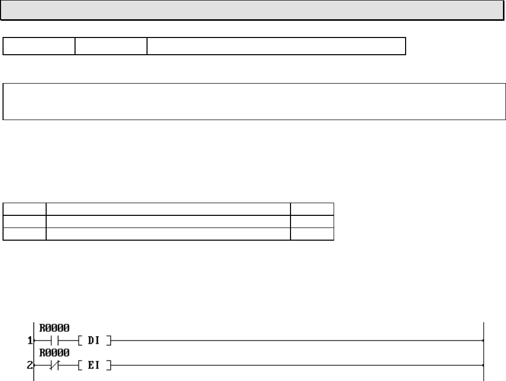
6F3B0253
Basic Hardware and Function 209
7. Instructions
FUN 141 DI Disable interrupt
Expression
Input −[ DI ]− Output
Function
When the input is ON, this instruction disables the execution of user designated interrupt operation,
i.e. timer interrupt program and I/O interrupt programs.
Execution condition
Input Operation Output
OFF No execution OFF
ON Execution ON
Operand
No operand is required.
Example
In the above example, the interrupt is disabled when R000 is ON, and it is enabled when R000
is OFF.
Note
• Refer to the EI instruction (FUN 140).
• If an interrupt factor is occurred during the interrupt disabled state, the interrupt is kept waiting
and it will be executed just after the EI instruction is executed.
• The DI instruction can be used only in the main program.
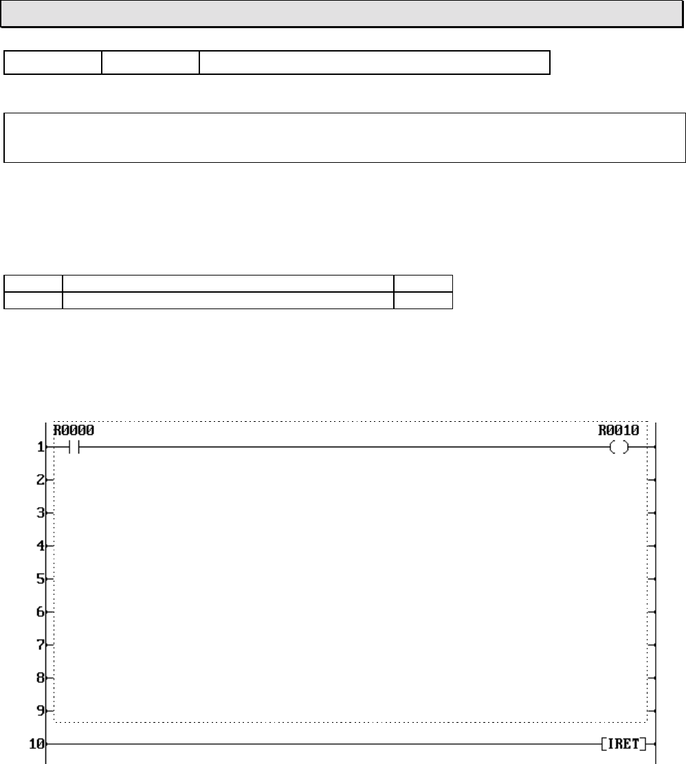
6F3B0253
210 T1-16S User’s Manual
7. Instructions
FUN 142 IRET Interrupt return
Expression
−−[ IRET ]−
Function
This instruction indicates the end of an interrupt program. When program execution reaches this
instruction, it returns to the original location of the main program (or subroutine).
Execution condition
Input Operation Output
-Execution -
Operand
No operand is required.
Example
Note
• The IRET instruction can be used only in an interrupt program.
• There is no specific instruction which indicates the beginning of the interrupt program.
An interrupt program
(Timer interrupt,
I/O interrupt #1, #2, #3 or #4)
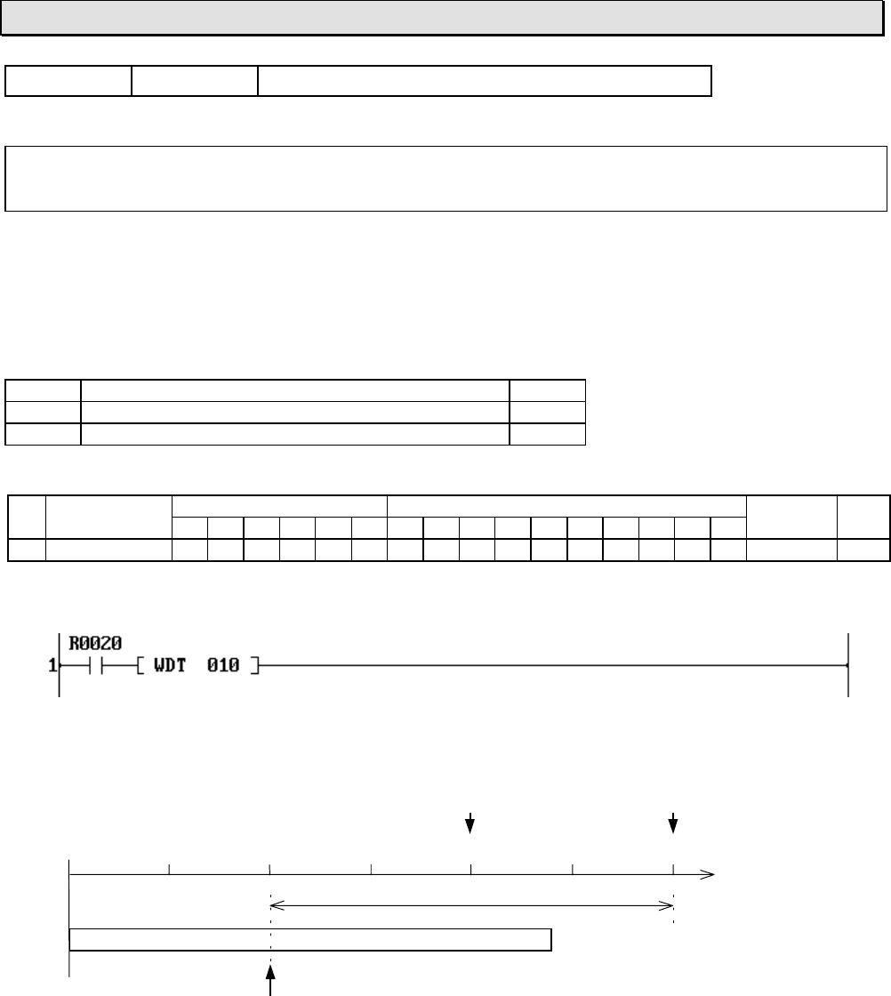
6F3B0253
Basic Hardware and Function 211
7. Instructions
FUN 143 WDT Watchdog timer reset
Expression
Input −[ WDT n ]− Output
Function
When the input is ON, this instruction extend the scan time over detection time by 200 ms.
Normally, T1/T1S detects the scan time-over if a scan is not finished within 200 ms. This instruction
can be used to extend the detection time.
Execution condition
Input Operation Output
OFF No execution OFF
ON Execution ON
Operand
Name Device Register Constant Index
X Y R S T. C. XWYWRWSW T C D I J K
nExtend time 1 - 100
Example
When R020 is ON, the scan time detection time is extended by 200 ms. The operand n has no
effect on the extended time. It is fixed as 200 ms.
Normal detection point Extended point
0 50 100 150 200 250 300 (ms)
Extended by 200 ms
Scan
WDT instruction
execution
Note
• As for the upper T-series PLCs, the operand n specifies the extended time. However in the
T1/T1S, it is fixed as 200 ms regardless of the operand n.
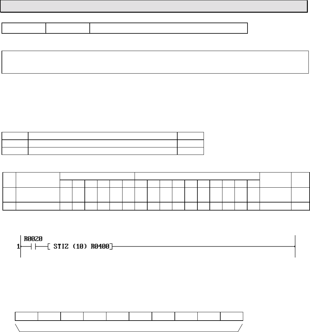
6F3B0253
212 T1-16S User’s Manual
7. Instructions
FUN 144 STIZ Step sequence initialize
Expression
Input −[ STIZ (n) A ]− Output
Function
When the input is ON, n devices starting with A are reset to OFF, and A is set to ON.
This instruction is used to initialize a series of step sequence. The step sequence is useful to
describe a sequential operation.
Execution condition
Input Operation Output
OFF No execution OFF
ON Execution at the rising edge of the input ON
Operand
Name Device Register Constant Index
X Y R S T. C. XWYWRWSW T C D I J K
nSize of step
sequence 1 - 64
AStart device √
Example
When R020 is changed from OFF to ON, R400 is set to ON and subsequent 9 devices (R401
to R409) are reset to OFF.
This instruction initializes a series of step sequence, 10 devices starting with R400.
R409 R408 R407 R406 R405 R404 R403 R402 R401 R400
OFF OFF OFF OFF OFF OFF OFF OFF OFF ON
10 devices starting with R400
Note
• The STIZ instruction is used together with STIN (FUN 145) and STOT (FUN 146) instructions to
configure the step sequence.
• The STIZ instruction is executed only when the input is changed from OFF to ON.
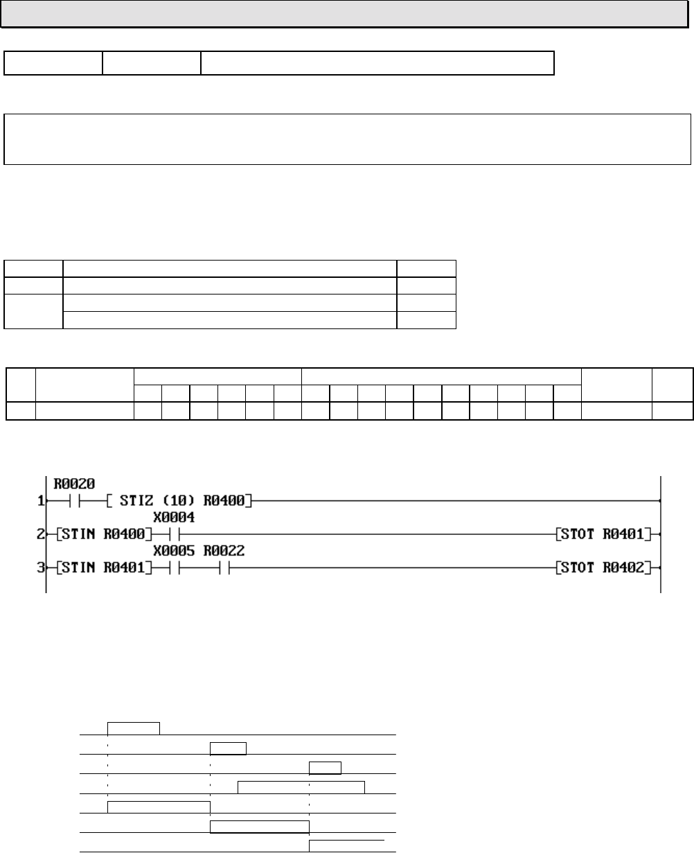
6F3B0253
Basic Hardware and Function 213
7. Instructions
FUN 145 STIN Step sequence input
Expression
Input −[ STIN A ]− Output
Function
When the input is ON and the device A is ON, the output is set to ON.
Execution condition
Input Operation Output
OFF No execution OFF
ON When A is ON ON
When A is OFF OFF
Operand
Name Device Register Constant Index
X Y R S T. C. XWYWRWSW T C D I J K
AStep device √
Example
The following sequential operation is performed.
When R020 is changed from OFF to ON, R400 is set to ON and subsequent 9 devices (R401
to R409) are reset to OFF.
When X004 comes ON, R400 is reset to OFF and R401 is set to ON.
When both X005 and R022 are ON, R401 is reset to OFF and R402 is set to ON.
R020
X004
X005
R022
R400
R401
R402
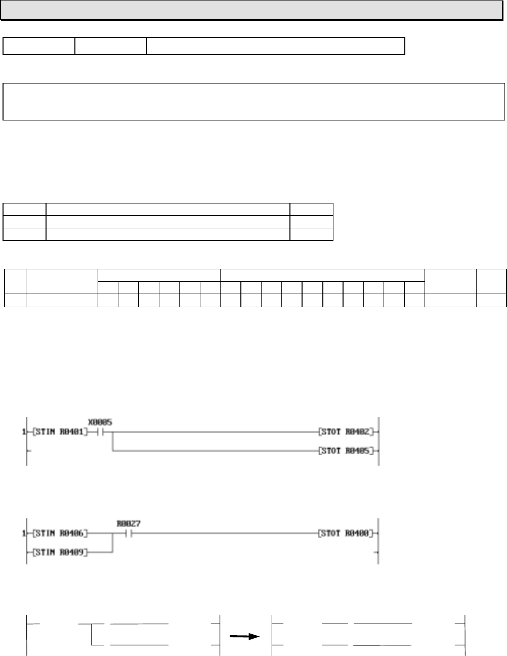
6F3B0253
214 T1-16S User’s Manual
7. Instructions
FUN 146 STOT Step sequence output
Expression
Input −[ STOT A ]−
Function
When the input is ON, the device A is set to ON and the devices of STIN instructions on the same
rung are reset to OFF.
Execution condition
Input Operation Output
OFF No execution -
ON Execution -
Operand
Name Device Register Constant Index
X Y R S T. C. XWYWRWSW T C D I J K
AStep device √
Example
See example on STIN (FUN 145) instruction.
Note
• The STIZ, STIN and STOT instructions are used together to configure the step sequence.
• Two or more STOT instructions can be placed on one rung to perform simultaneous sequences.
• Two or more STIN instructions can be placed on one rung in parallel or in series to perform loop
or convergence of sequences. (Max. 11 STIN instructions on one rung)
• To perform the conditional branch (sequence selection), separate the rungs as follows.
This limitation is applied to T1 version 1.00 only.
[ STIN A ] | | [ STOT B ] [ STIN A ] | | [ STOT B ]
| | [ STOT C ] [ STIN A ] | | [ STOT C ]
Not allowed Available
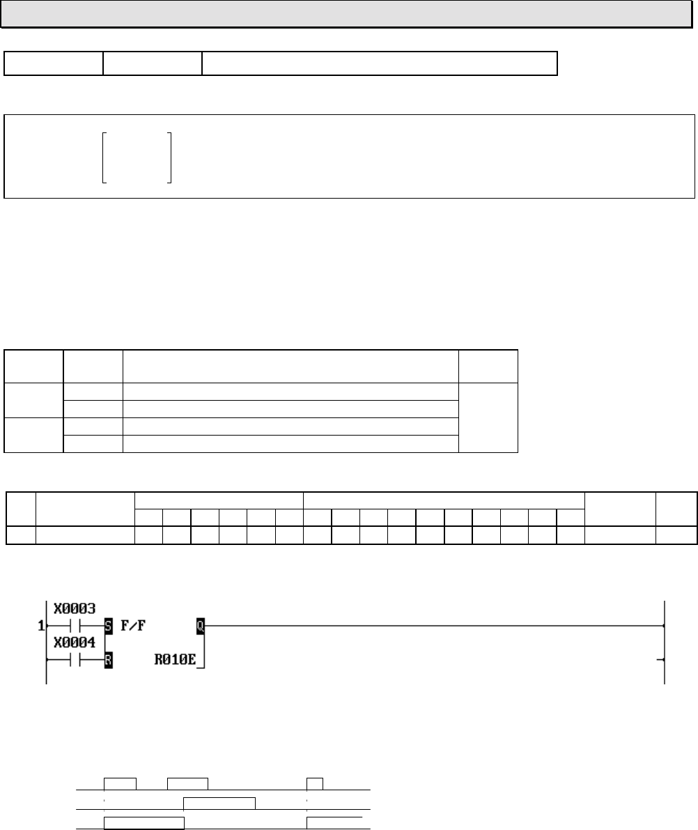
6F3B0253
Basic Hardware and Function 215
7. Instructions
FUN 147 F/F Flip-flop
Expression
Set input − S F/F Q − Output
Reset input − R A
Function
When the set input is ON, the device A is set to ON. When the reset input is ON, the device A is
reset to OFF. When both the set and reset inputs are OFF, the device A remains the state. If both
the set and reset inputs are ON, the device A is reset to OFF.
The state of the output is the same as the device A.
Execution condition
Set
input Reset
input Operation Output
OFF OFF No execution (A remains previous state) Same
ON Resets A to OFF as A
ON OFF Sets A to ON
ON Resets A to OFF
Operand
Name Device Register Constant Index
X Y R S T. C. XWYWRWSW T C D I J K
ADevice √√√
Example
When X003 is ON, R10E is set to ON. When X004 is ON, R10E is reset to OFF. If both are
ON, R10E is reset to OFF.
An example timing diagram is shown below.
X003
X004
R10E
Note
• For the set input, direct linking to a connecting point is not allowed. In this case, insert a dummy
contact (always ON = S04F, etc.) just before the input. Refer to Note of Shift register FUN 074.
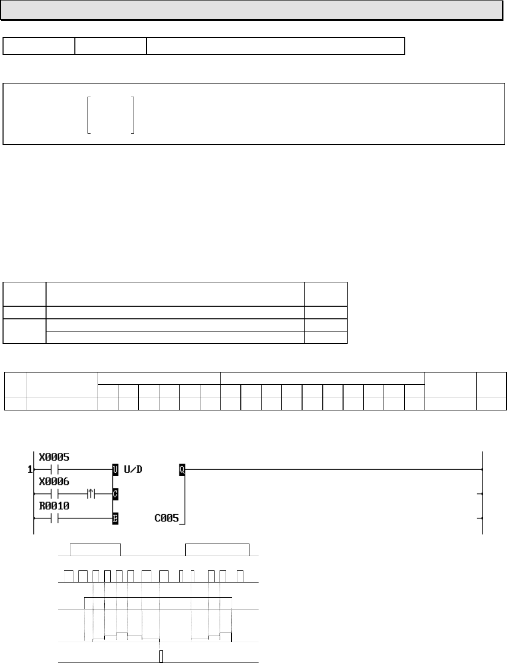
6F3B0253
216 T1-16S User’s Manual
7. Instructions
FUN 149 U/D Up-down counter
Expression
Direction input − U U/D Q − Output
Count input − C
Enable input − E A
Function
While the enable input is ON, this instruction counts the number of the count input changes from
OFF to ON. The count direction (up count or down count) is selected by the state of the direction
input. The count value is stored in the counter register A. The count value range is 0 to 65535.
• Up count when the direction input is ON
• Down count when the direction input is OFF
When the enable input is OFF, the counter register A is cleared to 0.
Execution condition
Enable
input Operation Output
OFF No operation (A is cleared to 0) OFF
ON Count value is not limit value (0 or 65535) OFF
Count value is limit value and count input is ON ON
Operand
Name Device Register Constant Index
X Y R S T. C. XWYWRWSW T C D I J K
ACount value √
Example
X005
X006
R010
C005
C.005
Note
• The transitional contact is required for
the count input. Otherwise, counting is
executed every scan during X005 is ON
in this example.
• For the direction input and the count
input, direct linking to a connecting point
is not allowed. Refer to Note of Shift
register FUN 074.
233 22 111
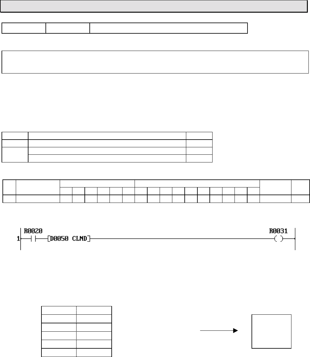
6F3B0253
Basic Hardware and Function 217
7. Instructions
FUN 154 CLND Set calendar
Expression
Input −[ A CLND ]− Output
Function
When the input is ON, the built-in clock/calendar is set to the date and time specified by 6 registers
starting with A. If an invalid data is contained in the registers, the operation is not executed and the
output is turned ON.
Execution condition
Input Operation Output
OFF No operation OFF
ON Execution (data is valid)) OFF
No execution (data is not valid) ON
Operand
Name Device Register Constant Index
X Y R S T. C. XWYWRWSW T C D I J K
AStart of table √√√√√√√
Example
When R020 is ON, the clock/calendar is set according to the data of D0050 to D0055, and the
output is OFF (R0031 is OFF).
If D0050 to D0055 contains invalid data, the setting operation is not executed and the output is
turned ON (R0031 comes ON).
F870
Allowable data range (2-digit BCD)
D0050 H00 Year H00 to H99 (1990 - 2089)
D0051 H00 Month H01 to H12
D0052 H00 Day H01 to H31 Calendar
D0053 H00 Hour H00 to H23 LSI
D0054 H00 Minute H00 to H59
D0055 H00 Second H00 to H59
Note
• The day of the week is automatically.
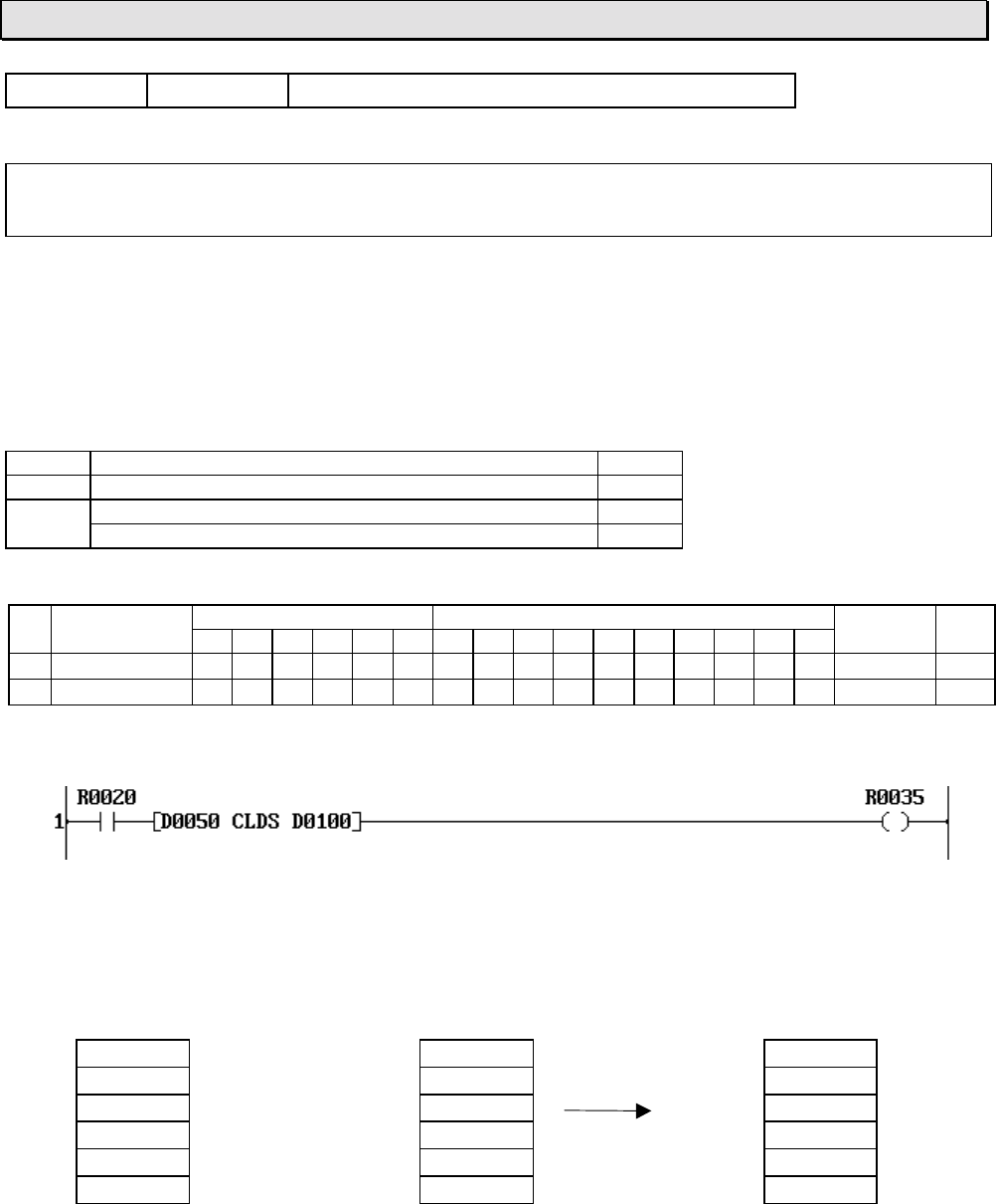
6F3B0253
218 T1-16S User’s Manual
7. Instructions
FUN 155 CLDS Calendar operation
Expression
Input −[ A CLDS B ]− Output
Function
When the input is ON, this instruction subtracts the date and time stored in 6 registers starting with
A from the current date and time, and stores the result in 6 registers starting with B.
If an invalid data is contained in the registers, the operation is not executed and the output is
turned ON.
Execution condition
Input Operation Output
OFF No operation OFF
ON Execution (data is valid)) OFF
No execution (data is not valid) ON
Operand
Name Device Register Constant Index
X Y R S T. C. XWYWRWSW T C D I J K
ASubtrahend √√√√√√√
BResult √√√√√√
Example
When R020 is ON, the date and time data recorded in D0050 to D0055 are subtracted from
the current date and time of clock/calendar, and the result is stored in D0100 to D0105.
In normal operation, the output is OFF (R0035 is OFF). If D0050 to D0055 contains invalid
data, the operation is not executed and the output is turned ON (R0035 comes ON).
F0 F0
H0098 D0050 H0097 D0100 H0000 (Year)
H0001 D0051 H0010 D0101 H0003 (Month)
H0015 minus D0052 H0010 D0102 H0007 (Day)
H0017 D0053 H0015 D0103 H0001 (Hour)
H0000 D0054 H0030 D0104 H0030 (Minute)
H0000 D0055 H0000 D0105 H0000 (Second)
Note
• Future date and time cannot be used as subtrahend A.
• In the calculation result, it means that 1 year is 365 days and 1 month is 30 days.
Current date & time

6F3B0253
Basic Hardware and Function 219
7. Instructions
FUN 156 PID3 Pre-derivative real PID
Expression
Input −[ A PID3 B → C ]− Output
Function
Performs PID (Proportional, Integral, Derivative) control which is a fundamental method of feed-
back control. (Pre-derivative real PID algorithm) This PID3 instruction has the following features.
• For derivative action, incomplete derivative is used to suppress interference of high-frequency
noise and to expand the stable application range,
• Controllability and stability are enhanced in case of limit operation for MV, by using digital PID
algorithm succeeding to benefits of analog PID.
• Auto, cascade and manual modes are supported in this instruction.
• Digital filter is available for PV.
• Direct / reverse operation is selectable.
Execution condition
Input Operation Output
OFF Initialization OFF
ON Execute PID every setting interval ON when
execution
Operand
Name Device Register Constant Index
X Y R S T. C. XW YW RW SW T C D I J K
ATop of input data √√√√√√√
BTop of parameter √√√√√√√
CTop of output data √√√√√√
Input data Control parameter Output data
AProcess input value PVC BProportional gain KPCManipulation value MV
A+1 A-mode set value ASV B+1 Integral time TIC+1 Last error en-1
A+2 C-mode set value CSV B+2 Derivative time TDC+2 Last derivative value Dn-1
A+3 M-mode MV input MMV B+3 Dead-band GP C+3 Last PV PVn-1
A+4 MV tracking input TMV B+4 A-mode initial SV ISV C+4 Last SV SVn-1
A+5 Mode setting MODE B+5 Input filter constant FT C+5 Integral remainder Ir
B+6 ASV differential limit DSV C+6 Derivative remainder Dr
B+7 MMV differential limit DMMV C+7 Internal MV MVn
A-mode: Auto mode B+8 Initial status STS C+8 Internal counter C
C-mode: Cascade mode B+9 MV upper limit MH C+9 Control interval ∆
∆∆
∆t
M-mode: Manual mode B+10 MV lower limit ML
B+11 MV differential limit DMV
B+12 Control interval setting n
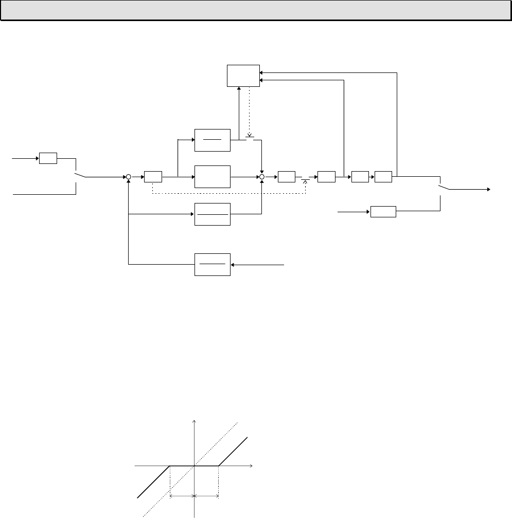
6F3B0253
220 T1-16S User’s Manual
7. Instructions
Control block diagram
1
TI⋅s
Differential limit
Derivative
Proportional
Integral
Differential ∆MVn
(η = 0.1)
MVS: Velocity → Position
MVn = MVn-1 ± ∆MVn
H/L: Upper / lower limit
DMV: Differential limit
MVCn
MVn
Manual
mode
Cascade
mode
Auto
mode
Digtal filter
MV
MMV
PVC
∆D
n
∆Pn
∆I
n
en
PVn
SVn
CSV
ASV
-
+
-
+
+
1
TD⋅s
1+η⋅TD⋅s
1
1+T⋅s
Gap KPMVS H/L DMV
DSV
DMMV
Integral
control
Integral action control:
When MV is limited (H/L, DMV) and the integral value has same sign as limit over, integral action
is stopped.
Velocity → Position conversion:
In Direct mode, MV increases when PV is increased. → MVn = MVn-1 - ∆Mvn
In Reverse mode, MV decreases when PV is increased. → MVn = MVn-1 + ∆MVn
Gap (dead-band) operation:
Error e
SV - PV
GP (%) GP (%)
Algorithm
Digital filter:
PV FT PVC FT PV
nn
=− ⋅ + ⋅ −
()11
Here, 0 000 0 999..≤≤FT
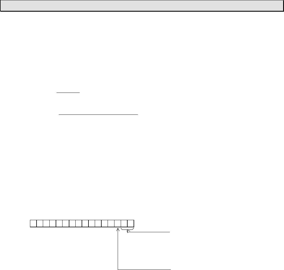
6F3B0253
Basic Hardware and Function 221
7. Instructions
PID algorithm:
∆∆∆∆
∆
MV K P I D
MV MV MV
nnnn
nn n
P
=⋅ ++
=±
−
()
1
Here, ∆Pee
eSVPV
nnn
nnn
=−
=−
−1
∆∆
IetIr
T
n
n
I
=⋅+
∆∆
∆
∆
DTPV PV tD Dr
tT
DD D
n
nn n
nn n
D
D
=⋅−−⋅+
+⋅
=+
=
−−
−
()
.
11
1
01
η
η
Parameter details
AProcess input value PVC (0.00 to 100.00 %) Data range: 0 to 10000
A+1 Auto mode set value ASV (0.00 to 100.00 %) Data range: 0 to 10000
A+2 Cascade mode set value CSV (0.00 to 100.00 %) Data range: 0 to 10000
A+3 Manual mode MV MMV (-25.00 to 125.00 %) Data range: -2500 to 12500
A+4 MV tracking input TMV (-25.00 to 125.00 %) Data range: -2500 to 12500
A+5 Mode setting MODE
FC840
Operation mode
00 : Manual mode
01 : Auto mode
10 : Cascade mode
11 : (Reserve)
Tracking designation
0 : No
1 : Yes
BProportional gain KP (0.00 to 327.67) Data range: 0 to 32767
B+1 Integral time TI (0.000 to 32.767 min., ∆In=0 if TI =0) Data range: 0 to 32767
B+2 Derivative time TD (0.000 to 32.767 min.) Data range: 0 to 32767
B+3 Gap (dead-band) GP (0.00 to 10.00 %) Data range: 0 to 1000
B+4 Auto mode initial set value ISV (0.00 to 100.00 %) Data range: 0 to 10000
B+5 Input filter constant FT (0.000 to 0.999) Data range: 0 to 999
B+6 ASV differential limit DSV (0.00 to 100.00 %/∆t) Data range: 0 to 10000
B+7 MMV differential limit DMMV (0.00 to 100.00 %/∆t) Data range: 0 to 10000
(If GP ≠ 0, Gap is applied)
(If TI = 0, then ∆In = 0)
(Fixed)
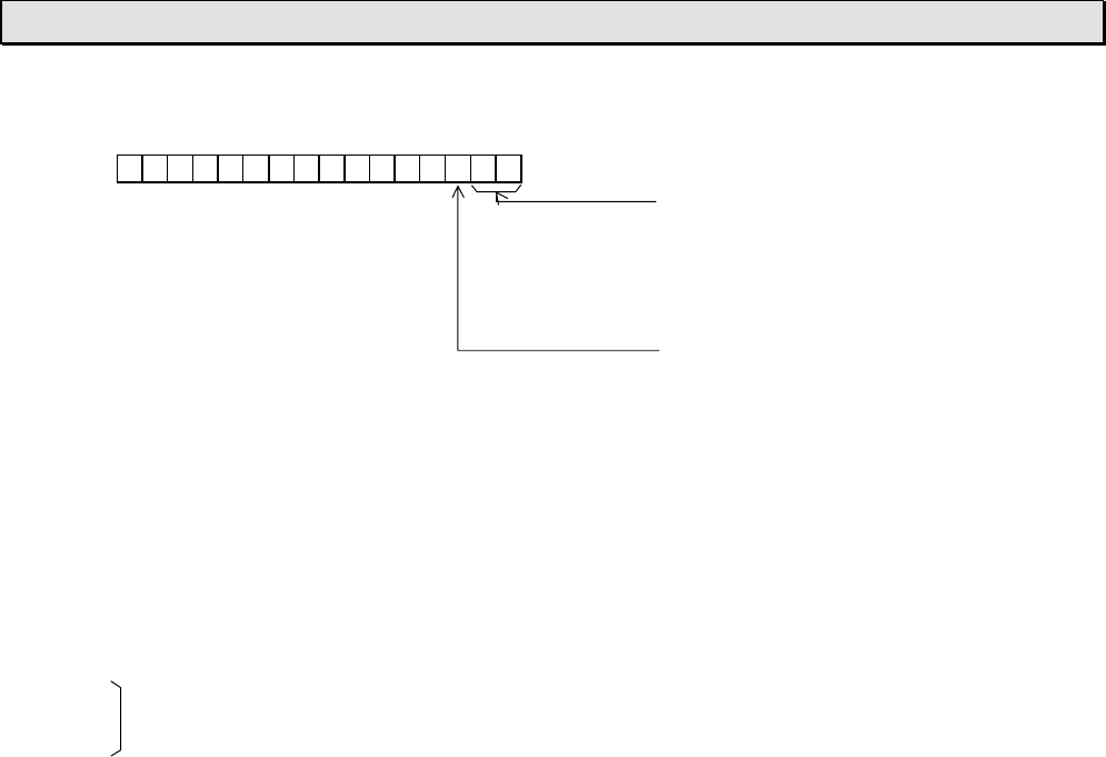
6F3B0253
222 T1-16S User’s Manual
7. Instructions
B+8 Initial status STS
FC840
Initial operation mode
00 : Manual mode
01 : Auto mode
10 : Cascade mode
11 : (Reserve)
Direct / reverse selection
0 : Direct
1 : Reverse
B+9 MV upper limit MH (-25.00 to 125.00 %) Data range: -2500 to 12500
B+10 MV lower limit ML (-25.00 to 125.00 %) Data range: -2500 to 12500
B+11 MV differential limit DMV (0.00 to 100.00 %/∆t) Data range: 0 to 10000
B+12 Control interval setting n (1 to 32767 times) Data range: 1 to 32767
Executes PID every n scan. Therefore, control interval ∆t = n × constant scan interval
(It is treated as n = 1 when n ≤ 0)
CManipulation value MV (-25.00 to 125.00 %) Data range: -2500 to 12500
C+1
: Internal work area
C+9
Operation
1. When the instruction input is OFF:
Initializes the PID3 instruction.
Operation mode is set as specified by B+8.A+5 bit 0, 1 ← B+8 bit 0, 1
Auto mode SV is set as specified by B+4. ASV ← ISV
Manual mode MV is set as current MV. MMV ← MV
Internal calculation data is initialized.
MV remains unchanged.
2. When the instruction input is ON:
Executes PID calculation every n scan which is specified by B+12. The following operation modes are
available according to the setting of A+5.
• Auto mode
This is a normal PID control mode with ASV as set value.
Set value differential limit DSV, manipulation value upper/lower limit MH/ML and differential limit DMV
are effective.
Bump-less changing from auto mode to manual mode is available. (Manual mode manipulation value
MMV is over-written by current MV automatically. MMV ← MV)

6F3B0253
Basic Hardware and Function 223
7. Instructions
• Manual mode
In this mode, the manipulation value MV can be directly controlled by the input value of MMV.
MV differential limit for manual mode DMMV is effective. MH/ML and DMV are not effective.
When mode is changed from manual to auto or cascade, the operation is started from the current MV.
• Cascade mode
This is a mode for PID cascade connection. PID is executed with CSV as set value.
Different from the auto mode, set value differential limit is not effective. Manipulation value upper/lower
limit MH/ML and differential limit DMV are effective.
Bump-less changing from cascade mode to manual mode is available. (Manual mode manipulation
value MMV is over-written by current MV automatically. MMV ← MV)
And, bump-less changing from cascade mode to auto mode is available. (Auto mode set value ASV is
over-written by current CSV automatically. ASV ← CSV)
• MV tracking
This function is available in auto and cascade modes. When the tracking designation (A+5 bit 2) is ON,
tracking input TMV is directly output as MV.
Manipulation value upper/lower limit MH/ML is effective, but differential limit DMV is not effective.
When the tracking designation is changed to OFF, the operation is started from the current MV.
Note
• PID3 instruction is only usable on the main-program.
• PID3 instruction must be used under the constant scan mode. The constant scan interval can be selected
in the range of 10 to 200 ms, 10 ms increments.
• The data handled by the PID3 instruction are % units. Therefore, process input value PVC, manipulation
value MV, etc., should be converted to % units (scaling), before and/or after the PID3 instruction. For this
purpose, the function generator instruction (FUN165 FG) is convenient.
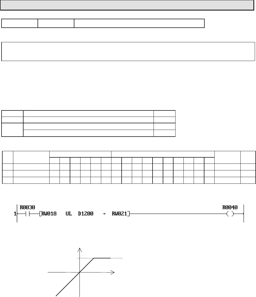
6F3B0253
224 T1-16S User’s Manual
7. Instructions
FUN 160 UL Upper limit
Expression
Input −[ A UL B → C ]− Output
Function
When the input is ON, the following operation is executed. (Upper limit for A by B)
If A ≤ B, then C = A.
If A > B, then C = B.
Execution condition
Input Operation Output
OFF No operation OFF
ON Execution: not limited (A ≤ B)OFF
Execution: limited (A > B)ON
Operand
Name Device Register Constant Index
X Y R S T. C. XWYWRWSW T C D I J K
AOperation data √√√√√√√√√√ √ √
BUpper limit √√√√√√√√√√ √ √
CDestination √√√√√√√√√ √
Example
When R030 is ON, the upper limit operation is executed for the data of RW018 by the data of
D1200, and the result is stored in RW021.
When RW018 is 3000 and D1200 is 4000, 3000 is stored in RW021 and R0040 is OFF.
When RW018 is 4500 and D1200 is 4000, the limit value 4000 is stored in RW021 and R0040
is ON.
Note
• This instruction deals with the data as signed integer (-32768 to 32767).
C
(RW021) Upper limit B (D1200)
A (RW018)
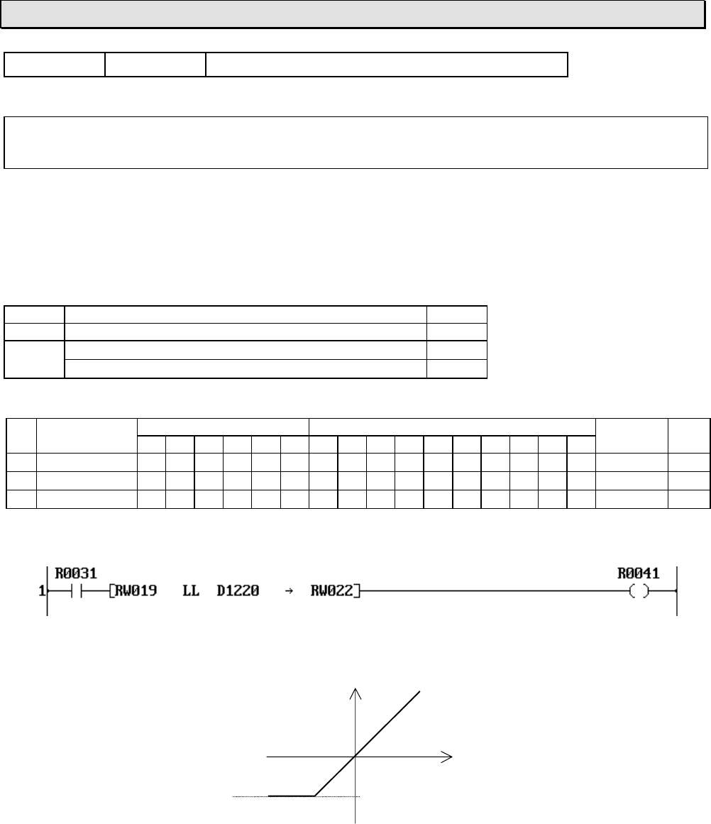
6F3B0253
Basic Hardware and Function 225
7. Instructions
FUN 161 LL Lower limit
Expression
Input −[ A LL B → C ]− Output
Function
When the input is ON, the following operation is executed. (Lower limit for A by B)
If A ≥ B, then C = A.
If A < B, then C = B.
Execution condition
Input Operation Output
OFF No operation OFF
ON Execution: not limited (A ≥ B)OFF
Execution: limited (A < B)ON
Operand
Name Device Register Constant Index
X Y R S T. C. XWYWRWSW T C D I J K
AOperation data √√√√√√√√√√ √ √
BLower limit √√√√√√√√√√ √ √
CDestination √√√√√√√√√ √
Example
When R031 is ON, the lower limit operation is executed for the data of RW019 by the data of
D1220, and the result is stored in RW022.
When RW019 is -1000 and D1220 is -1800, -1000 is stored in RW022 and R0041 is OFF.
When RW019 is 800 and D1220 is 1200, the limit value 1200 is stored in RW022 and R0041
is ON.
Note
• This instruction deals with the data as signed integer (-32768 to 32767).
C
(RW022)
Lower limit B (D1220)
A (RW019)
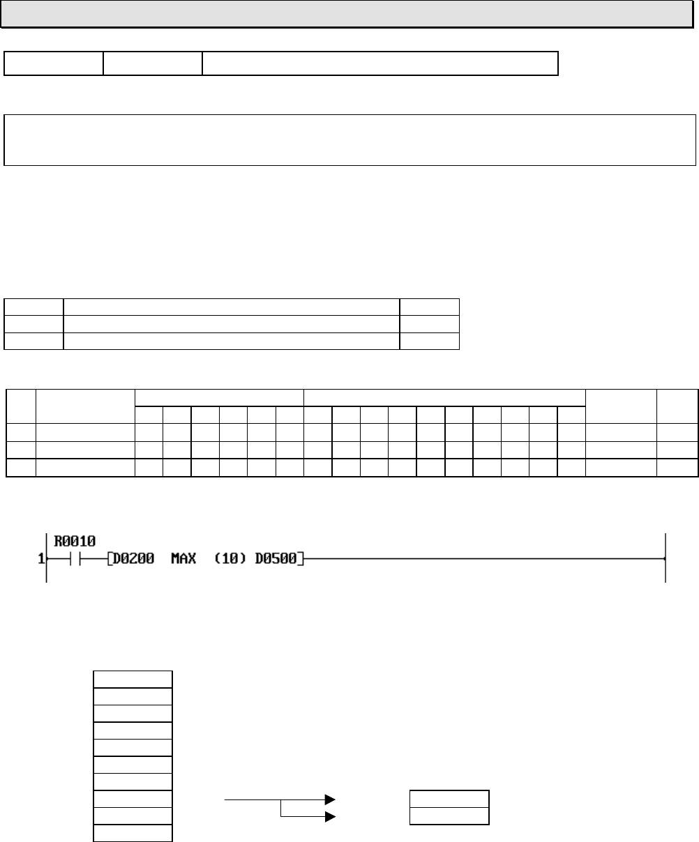
6F3B0253
226 T1-16S User’s Manual
7. Instructions
FUN 162 MAX Maximum value
Expression
Input −[ A MAX (n) B ]− Output
Function
When the input is ON, this instruction searches for the maximum value from the table of size n
words starting with A, and stores the maximum value in B and the pointer indicating the position of
the maximum value in B+1. The allowable range of the table size n is 1 to 64.
Execution condition
Input Operation Output
OFF No execution OFF
ON Execution ON
Operand
Name Device Register Constant Index
X Y R S T. C. XWYWRWSW T C D I J K
AStart of table √√√√√√√
nTable size 1 - 64
BResult √√√√√√√√√
Example
When R010 is ON, the maximum value is found from the register table D0200 to D0209 (10
words), and the maximum value is stored in D0500 and the pointer is stored in D0501.
Pointer
D0200 100 0
D0201 10000 1
D0202 -1000 2
D0203 10 3
D0204 0 4
D0205 200 5
D0206 -300 6
D0207 20000 7 D0500 20000 (Maximum value)
D0208 -30 8 D0501 7 (Pointer)
D0209 20 9
Note
• This instruction deals with the data as signed integer (-32768 to 32767).
• If there are two or more maximum value in the table, the lowest pointer is stored.
• If Index register K is used as operand B, the pointer data is discarded.
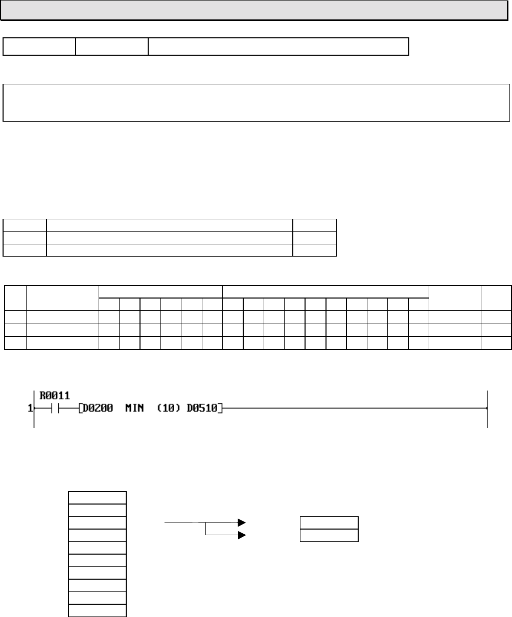
6F3B0253
Basic Hardware and Function 227
7. Instructions
FUN 163 MIN Minimum value
Expression
Input −[ A MIN (n) B ]− Output
Function
When the input is ON, this instruction searches for the minimum value from the table of size n
words starting with A, and stores the minimum value in B and the pointer indicating the position of
the minimum value in B+1. The allowable range of the table size n is 1 to 64.
Execution condition
Input Operation Output
OFF No execution OFF
ON Execution ON
Operand
Name Device Register Constant Index
X Y R S T. C. XWYWRWSW T C D I J K
AStart of table √√√√√√√
nTable size 1 - 64
BResult √√√√√√√√√
Example
When R011 is ON, the minimum value is found from the register table D0200 to D0209 (10
words), and the minimum value is stored in D0510 and the pointer is stored in D0511.
Pointer
D0200 100 0
D0201 10000 1
D0202 -1000 2 D0510 -1000 (Minimum value)
D0203 10 3 D0511 2 (Pointer)
D0204 0 4
D0205 200 5
D0206 -300 6
D0207 20000 7
D0208 -30 8
D0209 20 9
Note
• This instruction deals with the data as signed integer (-32768 to 32767).
• If there are two or more minimum value in the table, the lowest pointer is stored.
• If Index register K is used as operand B, the pointer data is discarded.
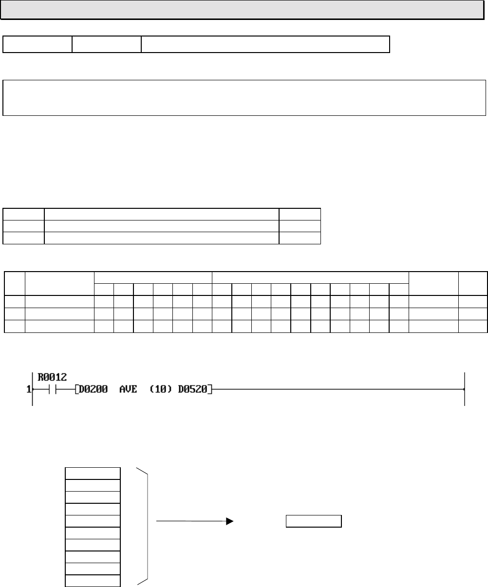
6F3B0253
228 T1-16S User’s Manual
7. Instructions
FUN 164 AVE Average value
Expression
Input −[ A AVE (n) B ]− Output
Function
When the input is ON, this instruction calculates the average value of the data stored in the n
registers starting with A, and stores the average value in B. The allowable range of the table size n
is 1 to 64.
Execution condition
Input Operation Output
OFF No execution OFF
ON Execution ON
Operand
Name Device Register Constant Index
X Y R S T. C. XWYWRWSW T C D I J K
AStart of table √√√√√√√
nTable size 1 - 64
BResult √√√√√√√√√
Example
When R012 is ON, the average value of the data stored in the register table D0200 to D0209
(10 words), and the average value is stored in D0520.
D0200 100
D0201 10000
D0202 -1000
D0203 10
D0204 0 D0520 2900 (Average value)
D0205 200
D0206 -300
D0207 20000
D0208 -30
D0209 20
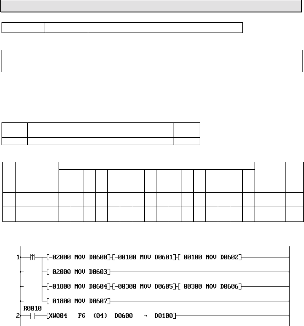
6F3B0253
Basic Hardware and Function 229
7. Instructions
FUN 165 FG Function generator
Expression
Input −[ A FG (n) B → C ]− Output
Function
When the input is ON, this instruction finds the function value f(x) for A as x, and stores it in C. The
function f(x) is defined by the parameters stored in 2 × n registers starting with B.
Execution condition
Input Operation Output
OFF No execution OFF
ON Execution ON
Operand
Name Device Register Constant Index
X Y R S T. C. XWYWRWSW T C D I J K
AInput value x√√√√√√√√√√ √
nParameter size 1 - 32
BStart of
parameters √√√√√√√
CFunction value
f(x) √√√√√√√√√
Example
When R010 is ON, the FG instruction finds the function value f(x) for x = XW004, and stores
the result in D0100.
The function f(x) is defined by 2 × 4 = 8 parameters stored in D0600 to D0607. In this example,
these parameters are set at the first scan.
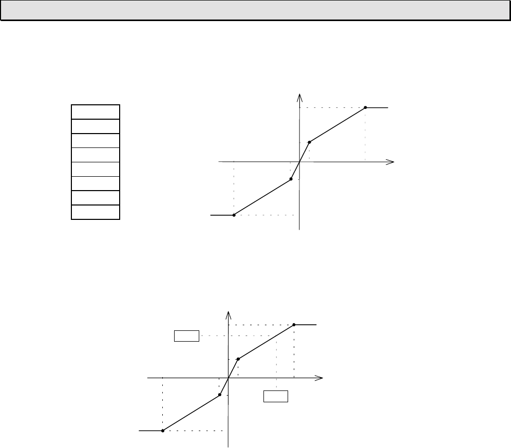
6F3B0253
230 T1-16S User’s Manual
7. Instructions
Parameter table
4 registers for x parameters and subsequent 4 registers for corresponding f(x) parameters
D0600 -2000 x1
D0601 -100 x2
D0602 100 x3
D0603 2000 x4
D0604 -1800 y1
D0605 -300 y2
D0606 300 y3
D0607 1800 y4
The FG instruction interpolators f(x) value for x based on the n parameters of (xi,yi).
For example, if XW04 is 1500 (x = 1500), the result 1405 (f(x) = 1405) is stored in D0100.
Note
• The order of the x parameters should be x1
≤
x2
≤
...
≤
xi
≤
...
≤
xn. In the above example, the
data of D0600 to D0603 should be D0600 ≤ D0601 ≤ D0602 ≤ D0603.
• If x is smaller than x1, y1 is given as f(x). In this example, D0604 data (-1800) is stored in
D0100 if XW04 is smaller than D0600 (-2000).
• If x is greater than xn, yn is given as f(x). In this example, D0607 data (1800) is stored in
D0100 if XW04 is greater than D0603 (2000).
• The valid data range is -32768 to 32767.
y(x4,y4)
1800
y = f(x)
300 (x3,y3)
x
2000100
-100-2000
(x2,y2)-300
(x1,y1)-1800
y
1800
1405
300
x
1500
2000100
-100-2000
-300
-1800
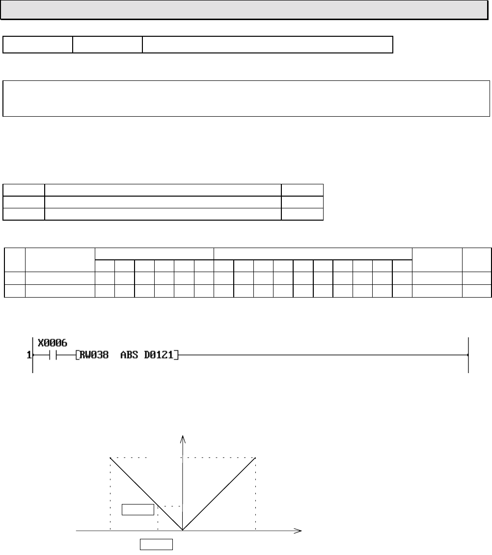
6F3B0253
Basic Hardware and Function 231
7. Instructions
FUN 180 ABS Absolute value
Expression
Input −[ A ABS B ]− Output
Function
When the input is ON, this instruction finds the absolute value of operand A, and stores it in B.
Execution condition
Input Operation Output
OFF No execution OFF
ON Execution ON
Operand
Name Device Register Constant Index
X Y R S T. C. XWYWRWSW T C D I J K
ASource √√√√√√√√√√ √
BDestination √√√√√√√√√
Example
When X006 is ON, the absolute value of RW38 is stored in D0121.
For example, if RW38 is -12000, the absolute value 12000 is stored in D0121.
Note
• The data range of A is -32768 to 32767. If the data of A is -32768, 32767 is stored in B.
32767
12000
0 32767-12000-32767
D0121
RW38
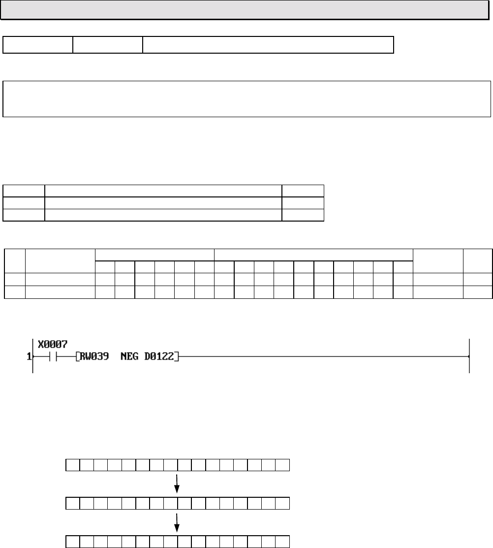
6F3B0253
232 T1-16S User’s Manual
7. Instructions
FUN 182 NEG 2’s complement
Expression
Input −[ A NEG B ]− Output
Function
When the input is ON, this instruction finds the 2’s complement value of A, and stores it in B.
Execution condition
Input Operation Output
OFF No execution OFF
ON Execution ON
Operand
Name Device Register Constant Index
X Y R S T. C. XWYWRWSW T C D I J K
ASource √√√√√√√√√√ √
BDestination √√√√√√√√√
Example
When X007 is ON, the 2’s complement value (sign inverted data) of RW39 is stored in D0122.
For example, if RW38 is 4660, the 2’s complement value -4660 is stored in D0122.
2’s complement data is calculated as follows.
FEDCBA9876543210
RW39 0001001000110100 (4660)
1110110111001011 (-4661)
D0122 1110110111001100 (-4660)
Note
• The data range of A is -32768 to 32767. If the data of A is -32768, the same data -32768 is
stored in B.
Bit inverse
+ 1
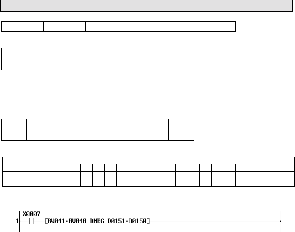
6F3B0253
Basic Hardware and Function 233
7. Instructions
FUN 183 DNEG Double-word 2’s complement
Expression
Input −[ A+1⋅A DNEG B+1⋅B ]− Output
Function
When the input is ON, this instruction finds the 2’s complement value of double-word data A+1⋅A,
and stores it in B+1⋅B.
Execution condition
Input Operation Output
OFF No execution OFF
ON Execution ON
Operand
Name Device Register Constant Index
X Y R S T. C. XWYWRWSW T C D I J K
ASource √√√√√√√ √
BDestination √√√√√√
Example
When X007 is ON, the 2’s complement value (sign inverted data) of double-word register
RW41⋅RW40 is stored in double-word register D0151⋅D0150.
For example, if RW41⋅RW40 is -1234567890, the 2’s complement value 1234567890 is stored
in D0151⋅D0150.
Note
• The data range of A+1⋅A is -2147483648 to 2147483647. If the data of A+1⋅A is -2147483648,
the same data -2147483648 is stored in B+1⋅B.
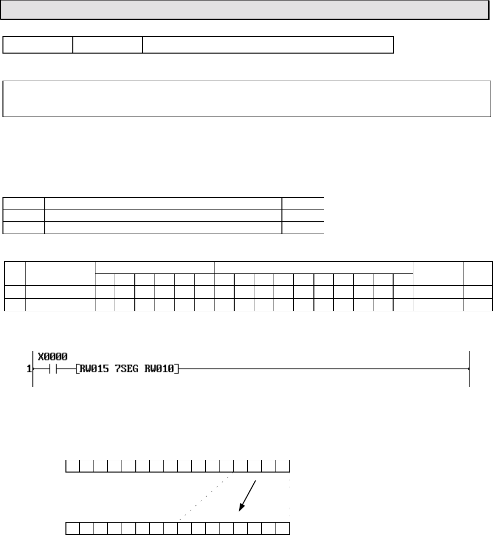
6F3B0253
234 T1-16S User’s Manual
7. Instructions
FUN 185 7SEG 7 segment decode
Expression
Input −[ A 7SEG B ]− Output
Function
When the input is ON, this instruction converts the lower 4 bits data of A into the 7 segment code,
and stores it in B. The 7 segment code is normally used for a numeric display LED.
Execution condition
Input Operation Output
OFF No execution OFF
ON Execution ON
Operand
Name Device Register Constant Index
X Y R S T. C. XWYWRWSW T C D I J K
ASource √√√√√√√√√√ √
BDestination √√√√√√√√√
Example
When X000 is ON, the lower 4 bits data of RW15 is converted into the 7 segment code, and
the result is stored in lower 8 bits of RW10. 0 is stored in upper 8 bits of RW10.
For example, if RW15 is H0009, the corresponding 7 segment code H006F is stored in RW10.
FEDCBA9876543210
RW15 0000000000001001 (H0009)
Upper 12 bits are ignored
RW10 0000000001101111 (H006F)
0 is stored in upper 8 bits
The 7 segment code conversion table is shown on the next page.
7 segment decode
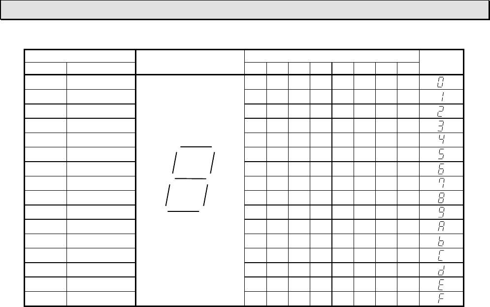
6F3B0253
Basic Hardware and Function 235
7. Instructions
Operand A (lower 4 bits) 7 segment LED Operand B (lower 8 bits) Display
Hex Binary composition B7B6B5B4B3B2B1B0
0 0000 0 0 1 1 1 1 1 1
1 0001 0 0 0 0 0 1 1 0
2 0010 0 1 0 1 1 0 1 1
3 0011 0 1 0 0 1 1 1 1
4 0100 0 1 1 0 0 1 1 0
5 0101 0 1 1 0 1 1 0 1
6 0110 0 1 1 1 1 1 0 1
7 0111 0 0 1 0 0 1 1 1
8 1000 0 1 1 1 1 1 1 1
9 1001 0 1 1 0 1 1 1 1
A 1010 0 1 1 1 0 1 1 1
B 1011 0 1 1 1 1 1 0 0
C 1100 0 0 1 1 1 0 0 1
D 1101 0 1 0 1 1 1 1 0
E 1110 0 1 1 1 1 0 0 1
F 1111 0 1 1 1 0 0 0 1
B0
B5 B1
B6
B4 B2
B3
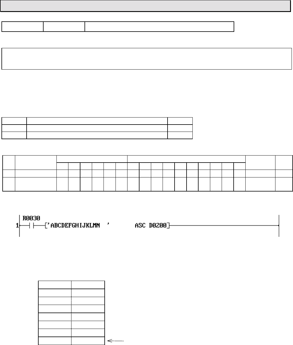
6F3B0253
236 T1-16S User’s Manual
7. Instructions
FUN 186 ASC ASCII conversion
Expression
Input −[ A ASC B ]− Output
Function
When the input is ON, this instruction converts the alphanumeric characters into the ASCII codes,
and stores them in the register table starting with B. (16 characters maximum)
Execution condition
Input Operation Output
OFF No execution OFF
ON Execution ON
Operand
Name Device Register Constant Index
X Y R S T. C. XWYWRWSW T C D I J K
ACharacters √
BStart of
destination √√√√√√
Example
When R030 is ON, the characters ‘ABCDEFGHIJKLMN’ is converted into the ASCII codes, and
the result is stored in 8 registers starting with lower 8 bits (byte) of D0200 (D0200 to D0207).
High Low
F 8 7 0
D0200 H42 (B) H41 (A)
D0201 H44 (D) H43 (C)
D0202 H46 (F) H45 (E)
D0203 H48 (H) H47 (G)
D0204 H4A (J) H49 (I)
D0205 H4C (L) H4B (K)
D0206 H4E (N) H4D (M)
D0207
Note
• Only the number of bytes converted are stored. The rest are not changed. In the above
example, 14 characters are converted into 14 bytes of ASCII code, and these ASCII codes are
stored in 7 registers (D0200 to D0206). The data of D0207 remains unchanged.
Previous data is remained
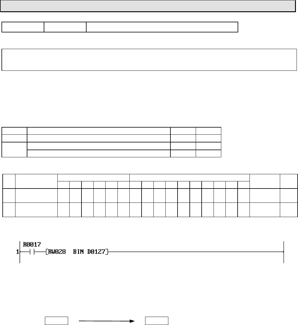
6F3B0253
Basic Hardware and Function 237
7. Instructions
FUN 188 BIN Binary conversion
Expression
Input −[ A BIN B ]− Output
Function
When the input is ON, this instruction converts the 4 digits of BCD data of A into binary, and stores
in B. If any digit of A contains non-BCD code (other than H0 through H9), the conversion is not
executed and the instruction error flag (ERF = S051) is set to ON.
Execution condition
Input Operation Output ERF
OFF No execution OFF −
ON Normal execution ON −
BCD data error OFF Set
Operand
Name Device Register Constant Index
X Y R S T. C. XWYWRWSW T C D I J K
ASource (BCD) √√√√√√√√√√H0000 -
H9999
BDestination
(Binary) √√√√√√√√√
Example
When R017 is ON, the BCD data of RW28 is converted into binary data, and the result is
stored in D0127.
For example, if RW28 is H1234, the binary data 1234 is stored in D0127.
RW28 BCD to Binary D0127
H1234 1234
Note
• If any digit of operand A contains non-BCD data, e.g. H13A6, the conversion is not executed
and the instruction error flag (ERF = S051) is set to ON.
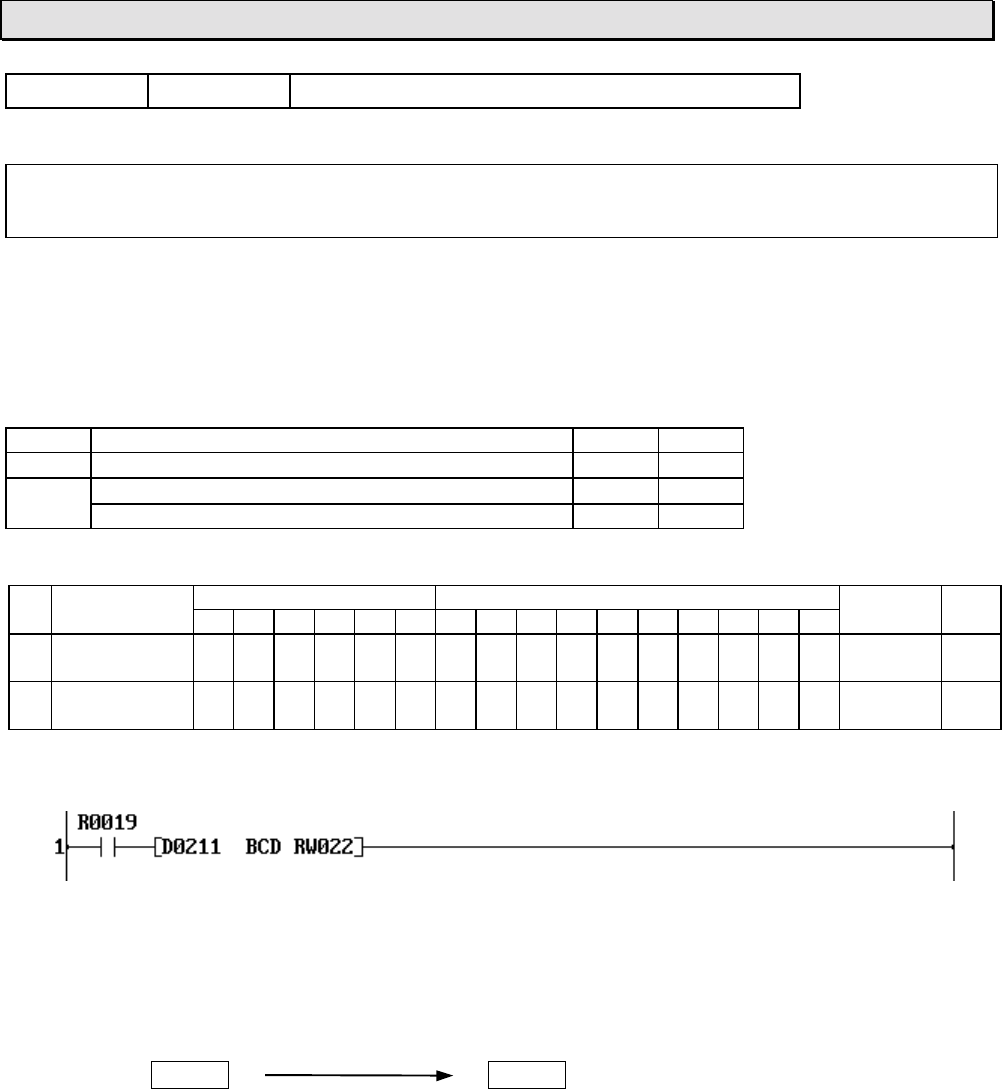
6F3B0253
238 T1-16S User’s Manual
7. Instructions
FUN 190 BCD BCD conversion
Expression
Input −[ A BCD B ]− Output
Function
When the input is ON, this instruction converts the binary data of A into BCD, and stores in B. If the
data of A is not in the range of 0 to 9999, the conversion is not executed and the instruction error
flag (ERF = S051) is set to ON.
Execution condition
Input Operation Output ERF
OFF No execution OFF −
ON Normal execution ON −
Binary data error OFF Set
Operand
Name Device Register Constant Index
X Y R S T. C. XWYWRWSW T C D I J K
ASource
(Binary) √√√√√√√√√√0 - 9999
BDestination
(BCD) √√√√√√√√√
Example
When R019 is ON, the data of D0211 is converted into 4-digit BCD, and the result is stored in
RW22.
For example, if D0211 is 5432, the BCD data H5432 is stored in RW22.
D0211 Binary to BCD RW22
5432 H5432
Note
• If the data of A is smaller than 0 or greater than 9999, the conversion is not executed and the
instruction error flag (ERF = S051) is set to ON.
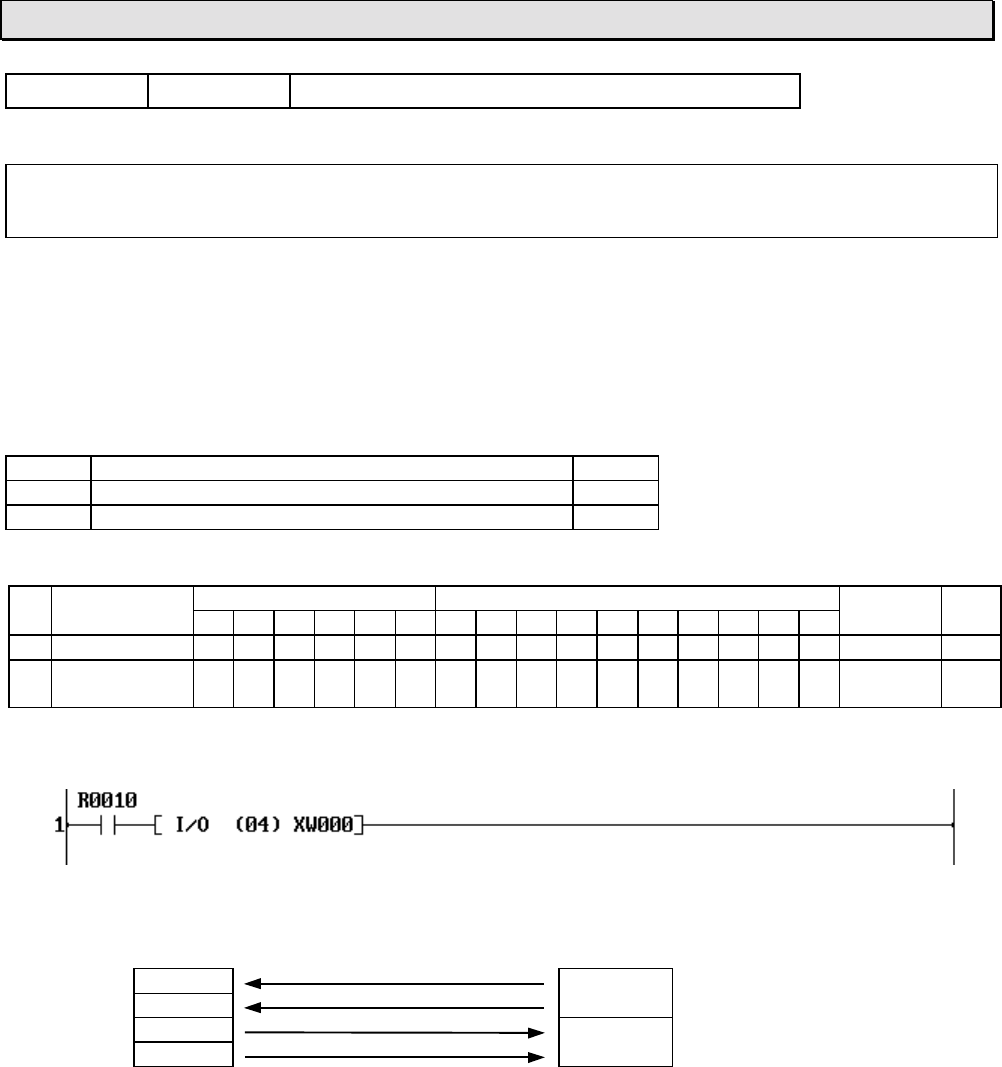
6F3B0253
Basic Hardware and Function 239
7. Instructions
FUN 235 I/O Direct I/O
Expression
Input −[ I/O (n) A ]− Output
Function
When the input is ON, this instruction immediately updates the external input (XW) and output
(YW) registers which are in the range of n registers starting with A.
• For XW register ... reads the data from corresponding input circuit
• For YW register ... writes the data into corresponding output circuit
Execution condition
Input Operation Output
OFF No execution OFF
ON Execution ON
Operand
Name Device Register Constant Index
X Y R S T. C. XWYWRWSW T C D I J K
nRegister size 1 - 32
AStart of
registers √√
Example
When R010 is ON, the 4 registers starting with XW00 (XW00 to YW03) are updated
immediately.
XW00 Input
XW01 circuit
YW02 Output
YW03 circuit

6F3B0253
240 T1-16S User’s Manual
7. Instructions
Note
• In the T1-16S, the following register/device range is only effective for this Direct I/O instruction.
Input on basic unit Output on basic unit I/O module
X000 - X007 Y020 - Y027 Not effective
• The Direct I/O instruction can be programmed in the main program and in the interrupt program.
If this instruction is programmed in both, the instruction in the main program should be executed
in interrupt disable state. Refer to EI (FUN 140) and DI (FUN 141) instructions.

6F3B0253
Basic Hardware and Function 241
7. Instructions
FUN 236 XFER Expanded data transfer
Expression
Input −[ A XFER B → C ]− Output
Function
When the input is ON, data block transfer is performed between the source which is indirectly
designated by A and A+1 and the destination which is indirectly designated by C and C+1. The
transfer size (number of words) is designated by B.
The transfer size is 1 to 256 words. (except for writing into EEPROM)
Data transfer between the following objects are available.
• CPU register (RW or D) ↔ EEPROM (D register)
• CPU register (RW or D) ↔ T1S RS-485 port (T1S only)
Execution condition
Input Operation Output ERF
OFF No execution OFF −
ON Normal execution ON −
When error is occurred (see Note) ON Set
Operand
Name Device Register Constant Index
X Y R S T. C. XWYWRWSW T C D I J K
ASource
parameter √√√√√√√
BTransfer size √√√√√√√
CDestination
parameter √√√√√√
Parameters
Source parameter Transfer size and status Destination parameter
AType BTransfer size CType
A+1 Leading address B+1 Status flag for RS-485 port C+1 Leading address
B+2 (max. 2 words)
Register type Type code Leading address Transfer size
RW register (RAM) H0003 0 to 255 1 to 256
D register (RAM) H0004 0 to 4095 1 to 256
D register (EEPROM) H0020 0 to 2047 1 to 32 (if destination)
1 to 256 (if source)
T1S RS-485 port H0030 0 (fixed) 1 to 256
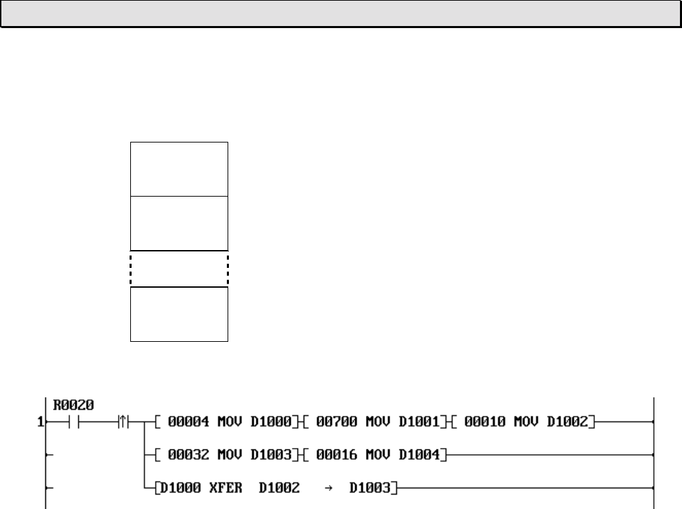
6F3B0253
242 T1-16S User’s Manual
7. Instructions
CPU register ↔
↔↔
↔ built-in EEPROM
In the EEPROM, the D registers are divided into pages as follows.
T1-16S
D0000 Page 1
(32 words)
D0031
D0032 Page 2
(32 words)
D0063
D2016 Page 64
(32 words)
D2047
Example
When R020 is changed from OFF to ON, 10 words of RAM data (D0700 to D0709) are written
into the EEPROM (D0016 to D0025).
D1000 (H0004) and D1001 (700) indicate the leading register of the source table (D0700 in
RAM). D1002 (10) indicates the transfer size (10 words = 10 registers). D1003 (H0020 = 32)
and D1004 (16) indicate the leading register of the destination table (D0016 in EEPROM).
Note
• The XFER instruction is not executed as error in the following cases. In these cases, the
instruction error flag (ERF = S051) is set to ON. If the ERF is set to ON once, it remains ON until
resetting to OFF by user program.
(1) When the number of words transferred exceeds limit.
(2) When the source/destination table of transfer is out of the valid range.
(3) When the transfer combination is invalid.
• The EEPROM has a life limit for data writing into an address. It is 100,000 times. Pay attention
not to exceed the limit. (EEPROM alarm flag = S007 is not updated by this instruction)
• Once data writing into the EEPROM is executed, EEPROM access (read/write) is prohibited for
the duration of 10 ms. Therefore, minimum 10 ms interval is necessary for data writing.
• The XFER instruction can be programmed in the main program and in the interrupt program.
If this instruction is programmed in both, the instruction in the main program should be executed
in interrupt disable state. Refer to EI (FUN 140) and DI (FUN 141) instructions.
• Writing data into the EEPROM is
available within one page at a
time. (max. 32 words)
• For data reading from the
EEPROM, there is no need to
consider the pages.
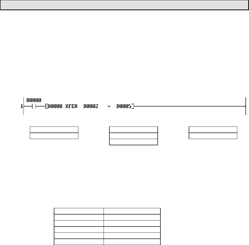
6F3B0253
Basic Hardware and Function 243
7. Instructions
CPU register ↔
↔↔
↔ T1S RS-485 port
<Receiving>
When the instruction input is ON, one set of message (from start character to the trailing code)
which is received by the RS-485 port is read from the receive buffer, and stored in the CPU
registers. The transfer size is fixed to 256 words. The execution status and the message length
(in bytes) are stored in the status flag.
The instruction input must be kept ON until the receiving operation is complete.
Example
Source designation Transfer size Destination designation
D0000 H0030 D0002 00256 (fixed) D0005 H0004
D0001 00000 D0003 Execution status D0006 00100
D0004 Message length
T1S RS-485 port D0100 (CPU register)
When R0000 is ON, one set of received message is read and stored in D0100 and after.
Execution status: H0000 ... Normal complete
H0001 ... Communication error (parity error, framing error)
H0002 ... Message length over (more than 512 bytes)
H0003 ... Receive buffer over flow
H0004 ... Receive time-out (from start character to the trailing code)
Baudrate Time-out setting
300, 600, 1200 bps 30 seconds
2400 bps 15 seconds
4800 bps 7 seconds
9600 bps 3 seconds
19200 bps 1.5 seconds
Message length: 0 .............. No receive message
1 to 512 ... Message length in bytes
Note
• The XFER instruction is not executed as error in the following cases. In these cases, the
instruction error flag (ERF = S051) is set to ON. If the ERF is set to ON once, it remains ON until
resetting to OFF by user program.
(1) The leading address for the RS-485 port designation is other than 0.
(2) Transfer size is other than 256.
(3) Mode setting of the RS-485 port is not the free ASCII mode.
(4) This instruction is programmed in the sub-program #1.
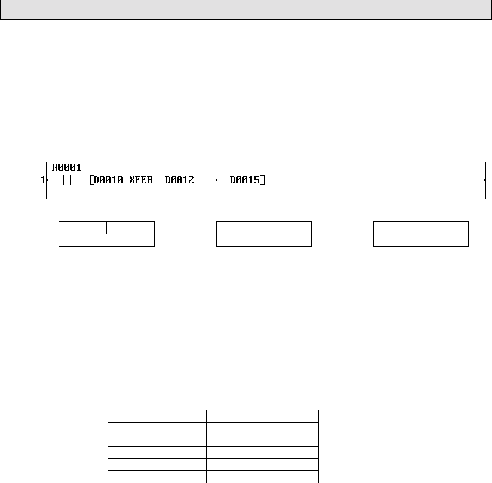
6F3B0253
244 T1-16S User’s Manual
7. Instructions
<Transmitting>
When the instruction input is ON, one set of message which is stored in the source table (from
start character to the trailing code) is transmitted through the RS-485 port. The execution
status is stored in the status flag.
The instruction input must be kept ON until the transmitting operation is complete.
Example
Source designation Transfer size Destination designation
D0010 H00 H04 D0012 00012 D0015 H00 H30
D0011 00500 D0013 Execution status D0016 00000
D0500 (CPU register) T1S RS-485 port
When R0001 is ON, one set of message (ended by the trailing code) stored in the range of
D0500 to D0511 (12 words) is transmitted through the RS-485 port.
Execution status: H0000 ... Normal complete
H0001 ... During transmitting the message
H0002 ... Communication busy
H0003 ... During the reset operation
H0004 ... Send time-out (from start character to the trailing code)
H0005 ... Send message length error (no trailing code in the source table)
Baudrate Time-out setting
300, 600, 1200 bps 30 seconds
2400 bps 15 seconds
4800 bps 7 seconds
9600 bps 3 seconds
19200 bps 1.5 seconds
Note
• The XFER instruction is not executed as error in the following cases. In these cases, the
instruction error flag (ERF = S051) is set to ON. If the ERF is set to ON once, it remains ON until
resetting to OFF by user program.
(1) The leading address for the RS-485 port designation is other than 0.
(2) Transfer size is out of the range of 1 to 256.
(3) Mode setting of the RS-485 port is not the free ASCII mode.
(4) This instruction is programmed in the sub-program #1.

6F3B0253
Basic Hardware and Function 245
7. Instructions
FUN 236 XFER Expanded data transfer (Inverter connection mode)
Expression
Input −[ A XFER B → C ]− Output
Function
This function is provided to control Toshiba Inverters VF-A7/G7/S9 connected on the RS-485 line.
When the RS-485 port operation mode is set to the Inverter mode (SW56 = 3), the T1-16S can
perform the following functions for up to 63 Inverters.
(1) Cyclically scans the Inverters and sends/receives the following data to/from each Inverter.
• Send to Inverter: Frequency reference write and Operation command write (Run, Stop, etc.)
• Receive from Inverter: Operating frequency monitor and Output terminal status monitor
(2) Cyclically scans the Inverters and receives the following data from each Inverter.
• Receive from Inverter: Operating frequency monitor and Output terminal status monitor
(3) Sends a specified Read command to a specified Inverter and stores the response data.
(4) Sends a specified Write command with the command data to a specified Inverter.
(5) Sends a specified Write command with the command data to all the connected inverters as
broadcast.
Execution condition
Input Operation Output ERF
OFF No execution OFF −
ON Normal execution ON −
When error is occurred (see Note) ON Set
Operand
Name Device Register Constant Index
X Y R S T. C. XWYWRWSW T C D I J K
AData table √√√√√√√
BInverter No. √√√√√√√
CRS-485 port √√√√√√
Parameters
Data table designation Parameter and status RS-485 port designation
ARegister type code BInverter number CFixed to H0030
A+1 Leading address B+1 Operation mode C+1 Fixed to 0
B+2 Execution status
B+3 Communication error code
B+4 Inverter communication
B+5 status map
B+6 (each bit shows each
B+7 Inverter status)
Data table designation (A, A+1):
Register Type code (A) Leading address (A+1)
RW register H0003 0 to 255
D register H0004 0 to 4095
6F3B0253
246 T1-16S User’s Manual
7. Instructions
Operation mode designation (B+1):
B+1 Operation mode Description
0 Data exchange mode
(Mode 0) Cyclically scans the connected Inverters (Control & Monitor)
(Inverter command: P+FA01&FA00 and R+FD00&FE07)
1 Monitor mode
(Mode 1) Cyclically scans the connected Inverters (Monitor only)
(Inverter command: R+FD00&FE07)
2 Read command mode
(Mode 2) Sends a read command to a specified Inverter
(Inverter command: R+ User designation)
3 Write command mode
(Mode 3) Sends a write command to a specified Inverter
(Inverter command: P+ User designation)
4 Broadcast mode
(Mode 4) Sends a write command to all the connected Inverters as broadcast
(Inverter command: P+ User designation)
Inverter number (B):
For the operation mode 0 and 1:
It specifies the maximum Inverter number. For example, if it is 5, the T1-16S scans from #0
through #5 Inverters and repeats. Setting range is 0 to 63.
For the operation mode 2 and 3:
It specifies the target Inverter number for sending commands. Setting range is 0 to 63.
For the operation mode 4:
This setting is ignored. The broadcast address (HFF) is used as Inverter number.
Execution status (B+2):
FEDCBA9876543210
B+2
Communication error code (B+3):
The communication error code responded from the Inverter is shown here. If 2 or more Inverters are error,
the smallest Inverter number's error is stored. Refer to Inverter's manual for the error code.
B+3 Meaning
0 No error (Normal)
Response time-out (No answer)
Others Inverter error response (Refer to Inverter's manual)
Inverter communication status map (B+4 to B+7):
This 4-word table shows the communication status map of each Inverter. (1: Normal / 0: Error or No
answer)
FEDCBA9876543210
B+4 1514131211109876543210
B+5 31 30 29 28 27 26 25 24 23 22 21 20 19 18 17 16
B+6 47 46 45 44 43 42 41 40 39 38 37 36 35 34 33 32
B+7 63 62 61 60 59 58 57 56 55 54 53 52 51 50 49 48
Shows the scan count.
(0 → 1 → 2 → ... → 32767 → 0 → 1 ... )
Comes 1 when the RS-485 port is busy. (No execution)
6F3B0253
Basic Hardware and Function 247
7. Instructions
< Data exchange mode (Mode 0) >
When the instruction input comes ON with the operand B+1 is 0, the Data exchange mode
(mode 0) is selected. In this mode, the T1-16S sends the following commands to the Inverters
starting from #0 through the Inverter number specified by the operand B, and repeats.
#0 Frequency reference write (FA01)
#0 Operation command write (FA00)
#1 Frequency reference write (FA01)
#1 Operation command write (FA00)
:
#n Frequency reference write (FA01)
#n Operation command write (FA00)
#0 Operating frequency monitor (FD00)
#0 Output terminal status monitor (FE07)
#1 Operating frequency monitor (FD00)
#1 Output terminal status monitor (FE07)
:
#n Operating frequency monitor (FD00)
#n Output terminal status monitor (FE07)
The maximum Inverter number #n is specified by the operand B.
The scan execution status and the Inverter communication status are stored in the operand
B+2 to B+7.
The command data table is specified by the operand A and A+1.
When the instruction input is reset to OFF, the operation is stopped after receiving the
response from the Inverter currently communicating.
Example
Data table designation Parameter & status RS-485 port
D1000 4 RW200 5 D1010 H0030 (fixed)
D1001 2000 RW201 0 (mode 0) D1011 0 (fixed)
RW202 Execution status
RW203 Comm error code
RW204
RW205 Inverter comms
RW206 status map
RW207
When the data for each operand are set as above, the following operation condition is specified.
•RW200=5 ⇒ The max Inverter number is 5. Therefore T1-16S scans from #0 through #5 Inverters.
•D1000=4 & D1001=2000 ⇒ D2000 is specified as the data table starting address.
Scan
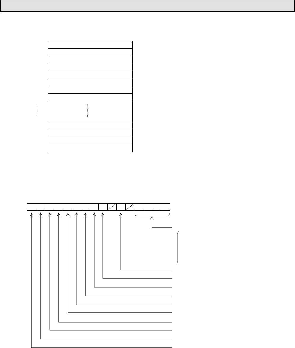
6F3B0253
248 T1-16S User’s Manual
7. Instructions
Data table:
Register Data contents Signal direction
D2000 #0 Operating frequency ← Read
D2001 #0 Output terminal status ← Read
D2002 #0 Frequency reference → Write
D2003 #0 Operation command → Write
D2004 #1 Operating frequency ← Read
D2005 #1 Output terminal status ← Read
D2006 #1 Frequency reference → Write
D2007 #1 Operation command → Write
D2020 #5 Operating frequency ← Read
D2021 #5 Output terminal status ← Read
D2022 #5 Frequency reference → Write
D2023 #5 Operation command → Write
•The data format for the operating frequency and the frequency reference registers are 0.01 Hz units.
For example, if it is 60 Hz, the corresponding register data is 6000.
•For the data format of the output terminal status register, refer to the Monitor mode (mode 1).
•The bit assignment of the operation command register is as follows. For details, refer to your
Inverter manual.
FEDCBA9876543210
Programmed speed selection
0000 = None
0001 = Speed 1
0010 = Speed 2
:
1111 = Speed 15
PI operation (0 = Normal / 1 = Off)
DC braking (0 = Off / 1 = On)
Jog operation (0 = off / 1 = On)
F/R selection (0 = Forward / 1 = Reverse)
Run/Stop (0 = Stop / 1 = Run)
Free run (0 = Normal / 1 = Free run)
Emergency stop (0 = Normal / 1 = EMS)
Reset command (0 = Normal / 1 = Reset)
Frequency enable (0 = Disable / 1 = Enable)
Command enable (0 = Disable / 1 = Enable)
Example operation:
To operate the #0 Inverter at 30 Hz forward rotation, write the value 3000 in D2002 and HC400 in
D2003. (HC400 = Bits F, E, A are 1, and others are 0)
The current operating frequency and the output terminal status of the #0 Inverter are stored in D2000
and D2001 respectively.
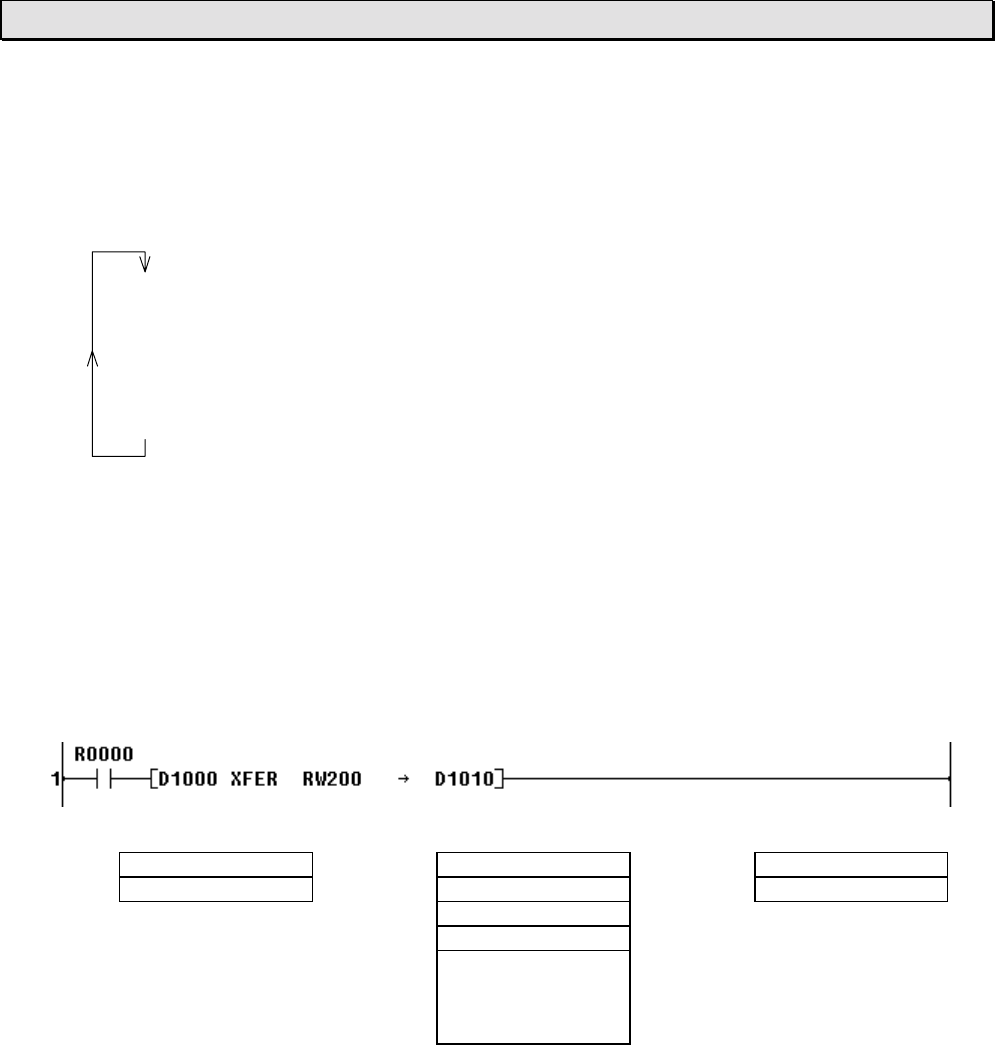
6F3B0253
Basic Hardware and Function 249
7. Instructions
< Monitor mode (Mode 1) >
When the instruction input comes ON with the operand B+1 is 1, the Monitor mode (mode 1) is
selected.
In this mode, the T1-16S sends the following Read commands to the Inverters starting from #0
through the Inverter number specified by the operand B, and repeats.
#0 Operating frequency monitor (FD00)
#0 Output terminal status monitor (FE07)
#1 Operating frequency monitor (FD00)
#1 Output terminal status monitor (FE07)
:
#n Operating frequency monitor (FD00)
#n Output terminal status monitor (FE07)
The maximum Inverter number #n is specified by the operand B.
The scan execution status and the Inverter communication status are stored in the operand
B+2 to B+7.
The monitor data table is specified by the operand A and A+1.
When the instruction input is reset to OFF, the operation is stopped after receiving the
response from the Inverter currently communicating.
Example
Data table designation Parameter & status RS-485 port
D1000 3 RW200 19 D1010 H0030 (fixed)
D1001 100 RW201 1 (mode 1) D1011 0 (fixed)
RW202 Execution status
RW203 Comm error code
RW204
RW205 Inverter comms
RW206 status map
RW207
When the data for each operand are set as above, the following operation condition is specified.
•RW200=19 ⇒ The max Inverter number is 19. Therefore T1-16S scans from #0 through #19 Inverters.
•D1000=3 & D1001=100 ⇒ RW100 is specified as the data table starting address.
Scan
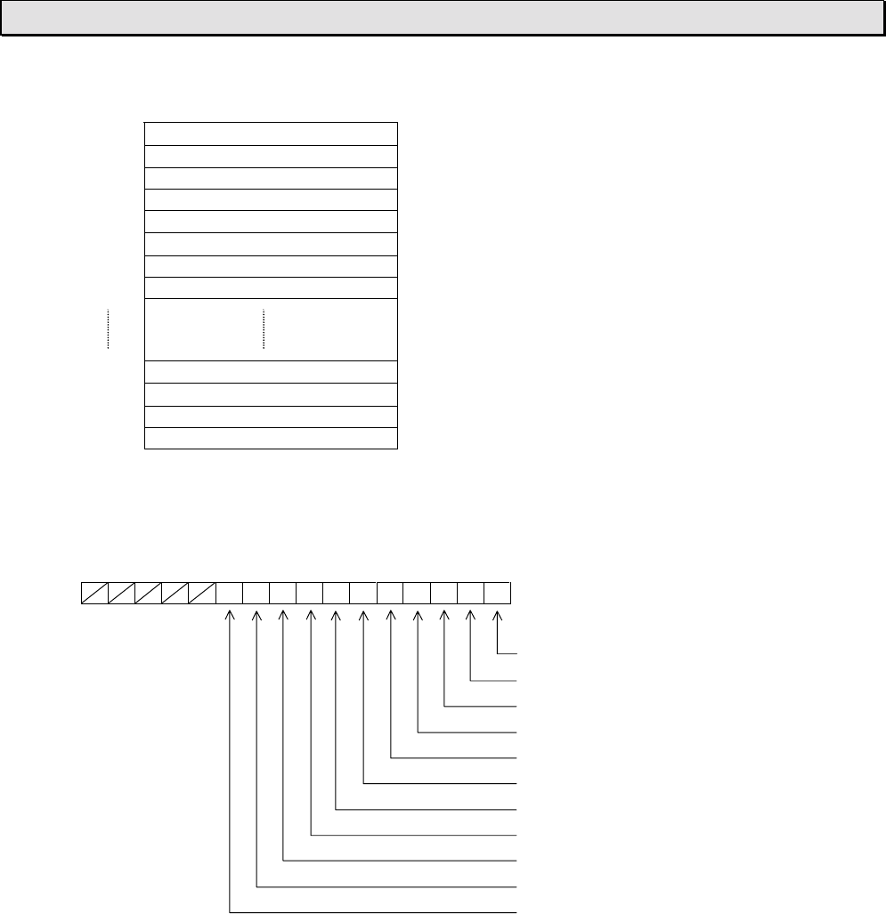
6F3B0253
250 T1-16S User’s Manual
7. Instructions
Data table:
Register Data contents Signal direction
RW100 #0 Operating frequency ← Read
RW101 #0 Output terminal status ← Read
RW102 No use
RW103 No use
RW104 #1 Operating frequency ← Read
RW105 #1 Output terminal status ← Read
RW106 No use
RW107 No use
RW176 #19 Operating frequency ← Read
RW177 #19 Output terminal status ← Read
RW178 No use
RW179 No use
•The data format for the operating frequency register is 0.01 Hz units. For example, if it is 60 Hz, the
corresponding register data is 6000.
•The bit assignment of the output terminal status register is as follows. For details, refer to your
Inverter manual.
FEDCBA9876543210
OUT1 (f130)
OUT2 (f131)
FL (f132)
R1 (f133)
R2 (f134)
OUT3 (f135)
OUT4 (f136)
ALM0
ALM1
ALM2
ALM3
Example operation:
The current operating frequency and the output terminal status of the #0 Inverter are stored in RW100
and RW101 respectively.
If the #0 Inverter is operating at 55 Hz, the data 5500 is stored in RW100. If the OUT2 terminal of the
#0 Inverter is ON, the bit 1 of RW101 (R1011) becomes 1.
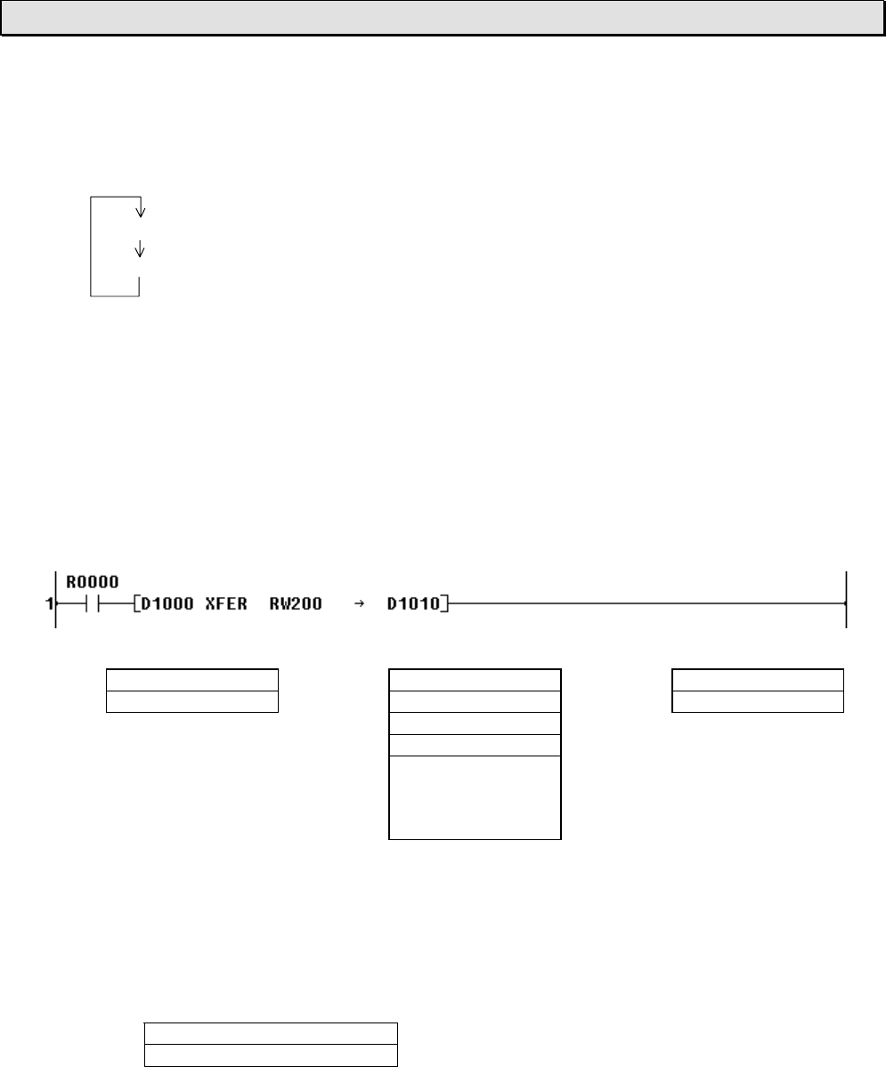
6F3B0253
Basic Hardware and Function 251
7. Instructions
< Read command mode (Mode 2) >
When the instruction input comes ON with the operand B+1 is 2, the Read command mode
(mode 2) is selected. In this mode, the T1-16S sends the user specified Read command to the
Inverter specified by the operand B, and repeats.
Sends the specified command to #n Inverter
Receives the response and stores the data into the register
The target Inverter number #n is specified by the operand B.
The scan execution status and the Inverter communication status are stored in the operand
B+2 to B+7.
The command setting register and the response data storing register is indirectly specified by
the operand A and A+1.
When the instruction input is reset to OFF, the operation is stopped after receiving the
response from the Inverter.
Example
Data table designation Parameter & status RS-485 port
D1000 4 RW200 3 D1010 H0030 (fixed)
D1001 3000 RW201 2 (mode 2) D1011 0 (fixed)
RW202 Execution status
RW203 Comm error code
RW204
RW205 Inverter comms
RW206 status map
RW207
When the data for each operand are set as above, the following operation condition is specified.
• RW200=3 ⇒ The target Inverter number is 3. Therefore T1-16S communicates with #3 Inverter.
• D1000=4 & D1001=3000 ⇒ D3000 is specified as the command setting register and D3001 is specified
as the response data storing register.
Data table:
Register Data contents Signal direction
D3000 Command code
D3001 Response data ← Read
Example operation:
For example, to read the output current from the #3 Inverter, set the command code HFE03 into
D3000. Then the response data is stored in D3001. If the response data is 1915, it means 19.15 %.
For the command code and the data format of the response, refer to your Inverter manual.
Repeat
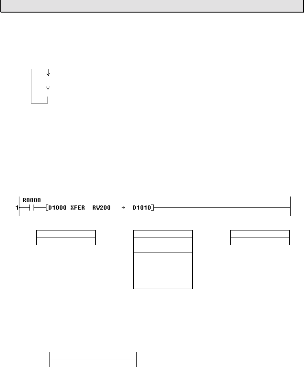
6F3B0253
252 T1-16S User’s Manual
7. Instructions
< Write command mode (Mode 3) >
When the instruction input comes ON with the operand B+1 is 3, the Write command mode
(mode 3) is selected. In this mode, the T1-16S sends the user specified Write command to the
Inverter specified by the operand B, and repeats.
Sends the specified command with command data to #n Inverter
Checks the acknowledge
The target Inverter number #n is specified by the operand B.
The scan execution status and the Inverter communication status are stored in the operand
B+2 to B+7.
The command code and the command data setting registers are indirectly specified by the
operand A and A+1.
When the instruction input is reset to OFF, the operation is stopped after receiving the
response from the Inverter.
Example
Data table designation Parameter & status RS-485 port
D1000 4 RW200 5 D1010 H0030 (fixed)
D1001 3010 RW201 3 (mode 3) D1011 0 (fixed)
RW202 Execution status
RW203 Comm error code
RW204
RW205 Inverter comms
RW206 status map
RW207
When the data for each operand are set as above, the following operation condition is specified.
• RW200=5 ⇒ The target Inverter number is 5. Therefore T1-16S communicates with #5 Inverter.
• D1000=4 & D1001=3010 ⇒ D3010 is specified as the command code setting register and D3011 is
specified as the command data setting register.
Data table:
Register Data contents Signal direction
D3010 Command code
D3011 Command data → Write
Example operation:
For example, to write the acceleration time parameter (10 seconds) to the #5 Inverter, set the
command code H0009 into D3010 and the value 100 into D3011.
For the command code and the command data format, refer to your Inverter manual.
Repeat
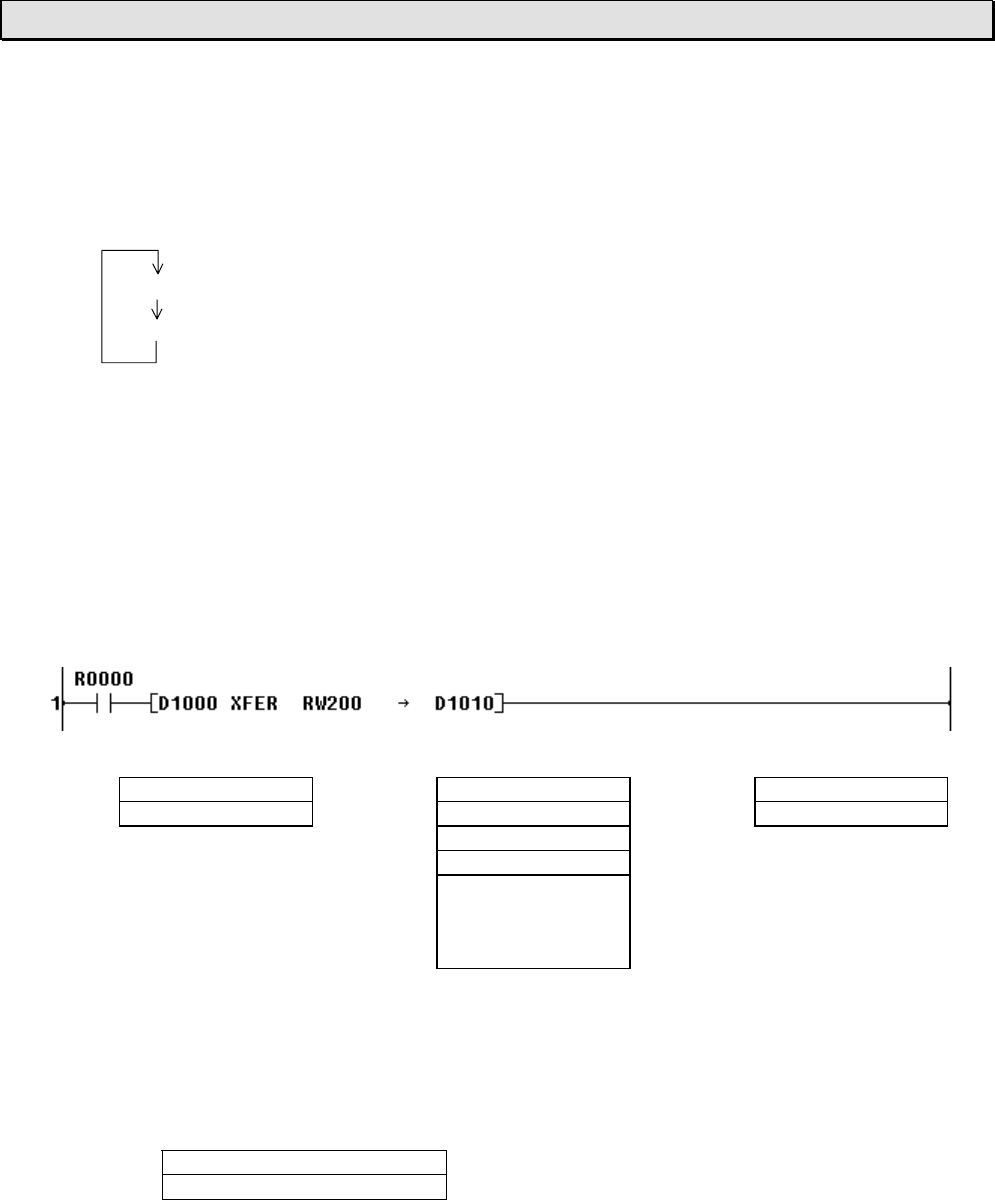
6F3B0253
Basic Hardware and Function 253
7. Instructions
< Broadcast mode (Mode 4) >
When the instruction input comes ON with the operand B+1 is 4, the Broadcast mode (mode 4)
is selected. In this mode, the T1-16S sends the user specified Write command to all the
Inverters as broadcast.
This mode is useful to send Run/Stop command to all the Inverter at the same time.
Sends the specified command with command data to all Inverters (broadcast)
Checks the acknowledge from #0 Inverter
The Inverter number specified by the operand B is ignored.
The scan execution status and the Inverter communication status are stored in the operand
B+2 to B+7. (only #0 Inverter responds)
The command code and the command data setting registers are indirectly specified by the
operand A and A+1.
When the instruction input is reset to OFF, the operation is stopped after receiving the
response from the Inverter.
Example
Data table designation Parameter & status RS-485 port
D1000 4 RW200 (any 0 to 63) D1010 H0030 (fixed)
D1001 3020 RW201 4 (mode 4) D1011 0 (fixed)
RW202 Execution status
RW203 Comm error code
RW204
RW205 Inverter comms
RW206 status map
RW207
When the data for each operand are set as above, the following operation condition is specified.
• D1000=4 & D1001=3020 ⇒ D3020 is specified as the command code setting register and D3021 is
specified as the command data setting register.
Data table:
Register Data contents Signal direction
D3020 Command code
D3021 Command data → Write
Example operation:
For example, to send the Run forward command to all the Inverters, set the command code HFA00
into D3020 and the value HC400 into D3021.
For the command code and the command data format, refer to your Inverter manual.
Repeat

6F3B0253
254 T1-16S User’s Manual
7. Instructions
< Note >
(1) The XFER instruction is not executed as error in the following cases. In these cases, the instruction error
flag (ERF = S051) is set to ON. If the ERF is set to ON once, it remains ON until resetting to OFF by
user program.
• The RS-485 port designation is other than H0030 and 0.
• The Inverter number designation is other than 0 to 63.
• Operation mode setting for RS-485 port is other than the Inverter connection mode.
(2) This XFER instruction must be programmed in the Main program.
(3) During the instruction input is ON, the data contents in the data table specified by A can be changed.
However, parameters specified by B cannot be changed.
(4) In the Data exchange mode (mode 0) and the Monitor mode (mode 1), the T1-16S scans from #0 to the
specified number. Therefore the Inverter number should be consecutive starting with 0.
If an Inverter is disconnected from the network, the T1-16S checks its existence periodically. When you
turn off power to an Inverter for maintenance purpose and turn on again, it is recommended to reset the
instruction input to re-configure the network.

6F3B0253
Basic Hardware and Function 255
Section 8
Special I/O Functions
8.1 Special I/O function overview, 256
8.2 Variable input filter constant, 260
8.3 High speed counter, 261
8.4 Interrupt input function, 268
8.5 Analog setting function, 270
8.6 Pulse output function, 271
8.7 PWM output function, 273

6F3B0253
256 T1-16S User’s Manual
8. Special I/O Functions
8.1 Special I/O function overview
The T1-16S supports the special I/O functions as listed below.
Function name Function summary Remarks
Variable input filter
constant Input filter constant (ON/OFF delay time) can be set
by user program. The setting range is 0 to 15ms
(1ms units). Default value is 10ms. This function is
applied for X000 to X007 (8 points as a block).
SW16 setting
is necessary to
use this
function. (Note)
Single phase
up-counter Counts the number of pulses of single phase pulse
train. 2 channels of pulse input are available. The
countable pulse rate is up to 5KHz for each channel.
Channel 1 … X000 count input, X002 reset input
Channel 2 … X001 count input, X003 reset input
Single phase
speed-
counter
Counts the number of pulses in a specified sampling
time. The sampling time setting is 10 to 1000ms
(10ms units). 2 channels of pulse input are available.
The countable pulse rate is up to 5KHz for each
channel.
Channel 1 … X000 count input
Channel 2 … X001 count input
High
speed
counter
Quadrature
bi-pulse
counter
Counts the 2-phase pulses whose phases are shifted
90° each other. Counts up when phase A precedes,
and counts down when phase B precedes.
The countable pulse rate is up to 5KHz.
Phase A …X000
Phase B …X001
Reset …… X002
Interrupt input function Immediately activates the corresponding I/O interrupt
program when the interrupt input is changed from
OFF to ON (or ON to OFF). 2 points of interrupt input
are available.
X002 …Interrupt 1 (I/O interrupt program #3)
X003 …Interrupt 2 (I/O interrupt program #4)
Only one
among these 4
functions can
be selected.
SW16 is used
to select the
function.(Note)
Analog setting
function The value of the analog setting adjuster is converted
into digital value (0 to 1000) and stored in the SW
register. 2 adjusters are provided on the T1-16S.
V0 … SW30
V1 … SW31
No function
selection is
required.
Pulse output function Variable frequency pulse train can be output. The
available pulse rate is 50 to 5000Hz (1Hz units).
Y020 … CW or Pulse (PLS)
Y021 … CCW or Direction (DIR)
PWM output function Variable duty cycle pulse train can be output. The
available ON duty setting is 0 to 100% (1% units).
Y020 … PWM output
Either one
between these
2 functions
can be used.
SW26 is used
to select the
function.(Note)

6F3B0253
Basic Hardware and Function 257
8. Special I/O Functions
Mode setting for the special I/O functions
These functions, except the analog setting function, are selected by setting data into
SW16 and SW26 by user program. These registers work as mode setting registers for
the special I/O functions. The data setting for these registers, i.e. mode setting for the
special I/O functions, is effective only at the first scan.
Note) In the explanation below, HSC and INT mean the high speed counter and the
interrupt input functions respectively.
FEDCBA9876543210
SW16 0 0 0 0 0
Bit 0 < HSC and INT master flag >
0: No use
1: Use
Bit 1 < HSC / INT selection >
0: INT
1: HSC
Bits 2 and 3 < INT No.1 mode >
00: No use (Reserve)
01: Rising (OFF to ON)
10: Falling (ON to OFF)
11: No use (Reserve)
Bits 6 and 7 < INT No.2 mode >
00: No use (Reserve)
01: Rising (OFF to ON)
10: Falling (ON to OFF)
11: No use (Reserve)
Bits A and B < HSC mode >
00: Single phase up-counter
01: Single phase speed-counter
10: Quadrature bi-pulse counter
11: No use (Reserve)
Bits C and D < Enable flag for HSC / INT >
00: CH2 - disable, CH1 - disable
01: CH2 - disable, CH1 - enable
10: CH2 - enable, CH1 - disable
11: CH2 - enable, CH1 - enable
Bit F < Variable input filter constant >
0: No use (fixed to 10ms)
1: Use
6F3B0253
258 T1-16S User’s Manual
8. Special I/O Functions
Note) In the explanation below, P-OUT means the pulse output function.
FEDCBA9876543210
SW26 0000000000
Bit 0 < P-OUT and PWM master flag >
0: No use
1: Use
Bit 1 < P-OUT / PWM selection >
0: PWM
1: P-OUT
Bit 2 < PLS mode >
0: CW/CCW
1: Pulse/Direction (PLS/DIR)
P-OUT / PWM operation error flag
(These are not user setting items)
Bit D < PWM pulse width error >
0: Normal
1: Error
Bit E < PWM ON duty setting error >
0: Normal
1: Error
Bit F < Frequency setting error >
0: Normal
1: Error
6F3B0253
Basic Hardware and Function 259
8. Special I/O Functions
The table below summarizes the mode setting data of each function. In the table,
‘−’ means do not care.
Variable input filter constant SW16
FEDCBA9876543210
Use 1 0 −−−−00−−00−−−−
High speed counter SW16
FEDCBA9876543210
Single phase Channel 1 only −001000000000011
up-counter Channel 2 only −010000000000011
Both channels −011000000000011
Single phase Channel 1 only −001010000000011
speed-counter Channel 2 only −010010000000011
Both channels −011010000000011
Quadrature bi-pulse counter −000100000000011
Interrupt input function SW16
FEDCBA9876543210
Interrupt 1 only Rising (OFF to ON) −001000000000101
Falling (ON to OFF) −001000000001001
Interrupt 2 only Rising (OFF to ON) −010000001000001
Falling (ON to OFF) −010000010000001
Both interrupts No.1 = Rising, No.2 = Rising −011000001000101
1 and 2 No.1 = Rising, No.2 = Falling −011000010000101
No.1 = Falling, No.2 = Rising −011000001001001
No.1 = Falling, No.2 =
Falling −011000010001001
Pulse output function SW26
FEDCBA9876543210
CW/CCW method −−−0000000000011
Pulse/Direction (PLS/DIR) method −−−0000000000111
PWM output function SW26
FEDCBA9876543210
Use −−−0000000000001
For example, the following programs can be used to select the quadrature bi-pulse
counter.
or
(H0803)
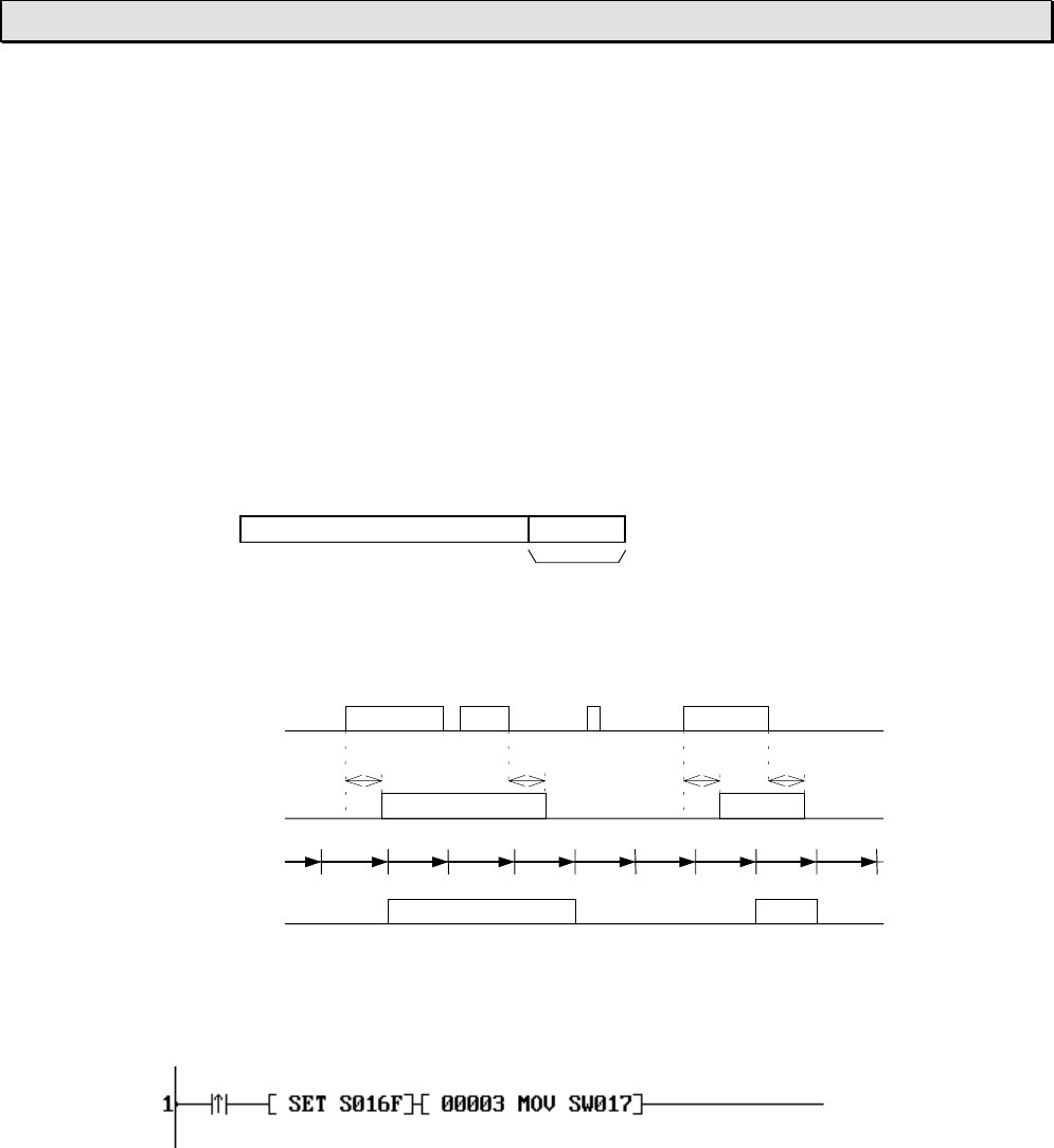
6F3B0253
260 T1-16S User’s Manual
8. Special I/O Functions
8.2 Variable input filter constant
Function
The input filter constant (ON/OFF delay time) of the leading 8 points X000 to X007
can be specified by user program within the range of 0 to 15ms. The default is 10ms.
The setting value is recognized at the first scan. Therefore, it cannot be changed after
the second scan.
Related registers
SW16 Function selection. Refer to section 8.1.
SW17 Input filter constant value
FEDCBA9876543210
No use (set to 0)
Setting value
0 to 15
Operation
Input signal
Internal logic
Scan cycle
X device
T: Input filter constant (0 to 15ms)
Sample program
This program sets the input filter constant to 3ms.
TTTT

6F3B0253
Basic Hardware and Function 261
8. Special I/O Functions
8.3 High speed counter
8.3.1 Single phase up-counter
Function
When the count input is changed from OFF to ON, the count value is increased by 1.
When the count value reaches the set value, the count value is reset to 0, and I/O
interrupt program is activated (if the interrupt enable flag is ON). The count value is
reset to 0 when the reset input comes ON.
This counter operation is enabled while the soft-gate is ON. The count value is reset to
0 when the soft-gate is changed from ON to OFF.
The set value is set internally at the timing of the soft-gate changing from OFF to ON.
When the soft-gate is OFF, the count value can be changed by writing the data into
the set value register and setting the count preset flag to ON.
The count value range is H0000 to HFFFF (16-bit data).
Hardware condition
Count input (X000 and X001)
ON/OFF pulse width: 100µs or more (max. 5KHz)
Reset input (X002 and X003)
ON/OFF duration: 2ms or more
Related registers
SW16: Function selection. Refer to section 8.1.
Function Register/device Remarks
Channel 1 Channel 2
Count input X000 X001 (Note)
Reset input X002 X003
Set value SW18 SW20 Data range: H0000 to HFFFF
Count value SW22 SW23
Soft-gate S240 S248 Operation is enabled when ON
Interrupt enable S241 S249 Interrupt is enabled when ON
Count preset S243 S24B Used to preset the counter value
Note) When both channels are used, X000 to X003 cannot be used as normal
input devices. However, if either one channel is used, these inputs for unused
channel can be used as normal input devices.
Interrupt assignment
Channel 1 … I/O interrupt program #1
Channel 2 … I/O interrupt program #2
6F3B0253
262 T1-16S User’s Manual
8. Special I/O Functions
Operation
Count input
Reset input
Soft-gate
Count value
Interrupt
Sample program
(H1003)
In this example, 4099 (H1003) is set in SW16. As a result, the single phase up-
counter (channel 1 only) is selected.
When R010 comes ON, the data 2000 is written into the set value register (SW18).
While R010 is ON, the soft-gate (S240) and the interrupt enable flag (S241) are set to
ON to enable the counter operation.
The counter works as a ring counter with the set value 2000. The count value is stored
in SW22.
When R010 is OFF and R011 comes ON, the count value is preset to the data of
D0100.
Set value
6F3B0253
Basic Hardware and Function 263
8. Special I/O Functions
8.3.2 Single phase speed-counter
Function
This function counts the number of changes of the count input from OFF to ON during
the every specified sampling time. The count value in a sampling time is stored in the
hold value register.
This counter operation is enabled while the soft-gate is ON. When the soft-gate is
OFF, the hold value is cleared to 0.
The setting range of the sampling time is 10 to 1000ms (10ms units).
The count value range is H0000 to HFFFF (16-bit).
Hardware condition
Count input (X000 and X001)
ON/OFF pulse width: 100µs or more (max. 5KHz)
Related registers
SW16: Function selection. Refer to section 8.1.
Function Register/device Remarks
Channel 1 Channel 2
Count input X000 X001 (Note 2)
Sampling time SW18 SW20 Data range: 1 to 100 (Note 1)
Hold value SW22 SW23 Data range: H0000 to HFFFF
Soft-gate S240 S248 Operation is enabled when ON
Note 1) The setting data range of the sampling time is 1 to 100. (10ms multiplier)
Note 2) When both channels are used, X000 and X001 cannot be used as normal
input devices. However, if either one channel is used, the input for unused
channel can be used as normal input devices.
Interrupt assignment
No interrupt function.
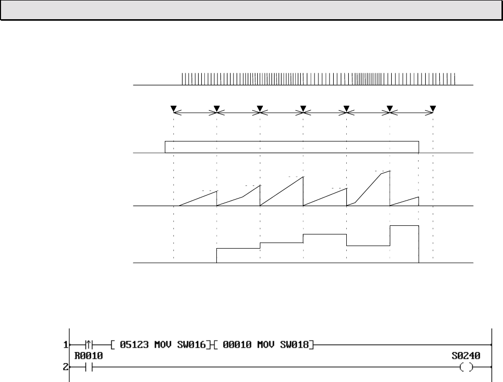
6F3B0253
264 T1-16S User’s Manual
8. Special I/O Functions
Operation
Count input
Sampling time
Soft-gate
Internal
count value
Hold value
Sample program
(H1403)
In this example, 5123 (H1403) is set in SW16. As a result, the single phase speed-
counter (channel 1 only) is selected.
The sampling time is set as 100ms, because 10 is written in SW18.
While R010 is ON, the soft-gate (S240) is set to ON, and the speed-counter works.
The hold value is stored in SW22.
∆T∆T∆T∆T∆T∆T
e
cd
b
a
e
d
c
b
a
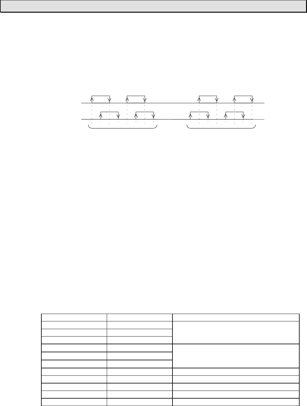
6F3B0253
Basic Hardware and Function 265
8. Special I/O Functions
8.3.3 Quadrature bi-pulse counter
Function
This function counts up or down the quadrature bi-pulse (2-phase pulses whose
phases are shifted 90° each other). Counts up when phase A precedes, and counts
down when phase B precedes. Both rising and falling edges of each phase are
counted. Consequently, 4 times count value against the pulse frequency is obtained.
Phase A
Phase B
Up count Down count
When the count value reaches the comparison value 1 (or 2), the I/O interrupt
program #1 (or #2) is activated (if the interrupt enable flag for each is ON).
This counter operation is enabled while the soft-gate is ON. The count value is reset to
0 when the soft-gate is changed from ON to OFF. The count value is also reset to 0
when the reset input comes ON.
When the soft-gate is OFF, the count value can be changed by writing the data into
the comparison value 1 (or 2) register and setting the count preset flag 1 (or 2) to ON.
The comparison value 1 and 2 can be changed even when the soft-gate is ON.
The count value range is -2147483648 to 2147483647 (32-bit data).
Hardware condition
Phase A and phase B (X000 and X001)
ON/OFF pulse width: 100µs or more (max. 5KHz)
Reset input (X002)
ON/OFF duration: 2ms or more
Related registers
SW16: Function selection. Refer to section 8.1.
Function Register/device Remarks
Phase A X000
Phase B X001
Reset input X002
Comparison value 1 SW19⋅SW18 Data range: -2147483648 to 2147483647
Comparison value 2 SW21⋅SW20
Count value SW23⋅SW22
Soft-gate S240 Operation is enabled when ON
Interrupt enable 1 S241 Interrupt 1 is enabled when ON
Count preset 1 S243 Used to preset the count value
Interrupt enable 2 S249 Interrupt 2 is enabled when ON
Count preset 2 S24B Used to preset the count value
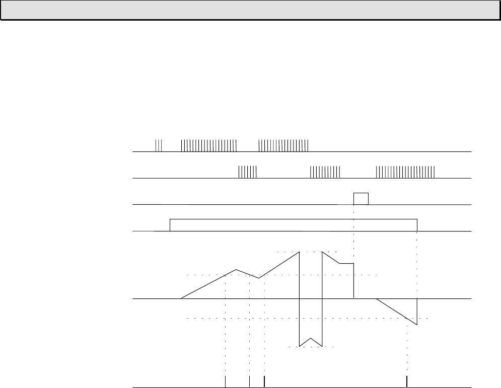
6F3B0253
266 T1-16S User’s Manual
8. Special I/O Functions
Interrupt assignment
Comparison value 1 … I/O interrupt program #1
Comparison value 2 … I/O interrupt program #2
Operation
Up count
Down count
Reset input
Soft-gate
Count value
Interrupt
2147483647
Comparison
value 1
Comparison
value 2
-2147483648
2111
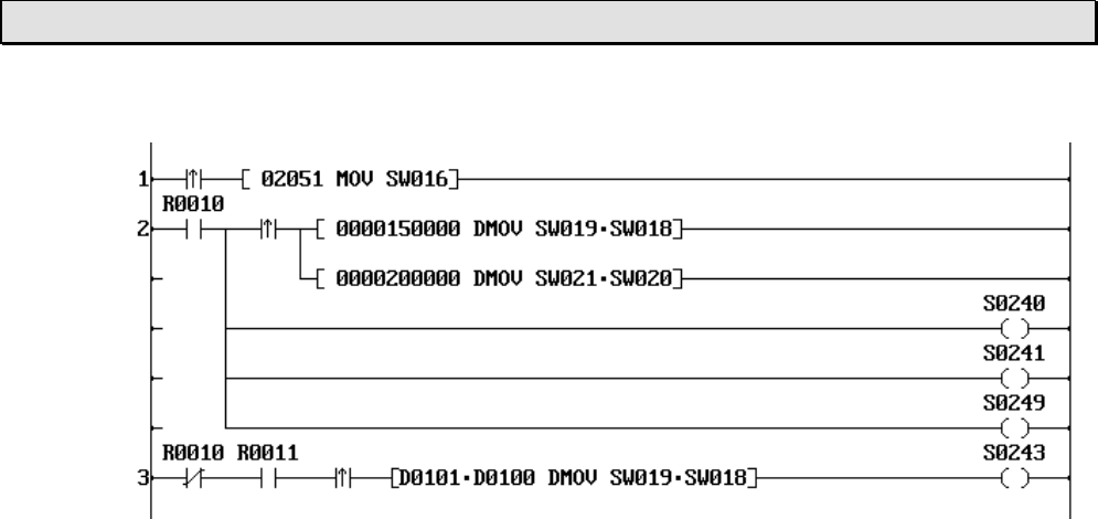
6F3B0253
Basic Hardware and Function 267
8. Special I/O Functions
Sample program
(H0803)
In this example, 2051 (H0803) is set in SW16. As a result, the quadrature bi-pulse
counter is selected.
When R010 comes ON, the data 150000 is set into the comparison value 1 register
(SW19⋅SW18), and 200000 is set into the comparison value 2 register (SW21⋅SW20).
While R010 is ON, the soft-gate (S240), the interrupt enable flag 1 (S241) and the
interrupt enable flag 2 (S249) are set to ON to enable the counter operation.
The count value is stored in SW23⋅SW22.
When R010 is OFF and R011 comes ON, the count value is preset to the data of
D0101⋅D0100.

6F3B0253
268 T1-16S User’s Manual
8. Special I/O Functions
8.4 Interrupt input function
Function
When the signal state of the interrupt input is changed from OFF to ON (or ON to
OFF), the corresponding I/O interrupt program is activated immediately.
Up to 2 interrupt inputs can be used. The interrupt generation condition can be
selected either rising edge (OFF to ON) or falling edge (ON to OFF) for each input.
The I/O interrupt program #3 is corresponding to the interrupt input 1, and the I/O
interrupt program #4 is corresponding to the interrupt input 2.
Hardware condition
Interrupt input (X002 and X003)
ON/OFF pulse width: 100µs or more
Related registers
SW16: Function selection. Refer to section 8.1.
Interrupt input 1 X002
Interrupt input 2 X003
Interrupt assignment
Interrupt input 1 … I/O interrupt program #3
Interrupt input 2 … I/O interrupt program #4
Operation
Interrupt input 1
Interrupt input 2
Interrupt
The above operation example is the case of rising edge setting for both inputs.
4433
6F3B0253
Basic Hardware and Function 269
8. Special I/O Functions
Sample program
Main program
(H3045)
I/O interrupt program #3
Interrupt program A
I/O interrupt program #4
Interrupt program B
In this example, 12357 (H3045) is set in SW16. As a result, the interrupt input function
(2 points, rising for both) is selected.
When X002 is changed from OFF to ON, the interrupt program A is executed. When
X003 is changed from OFF to ON, the interrupt program B is executed.
Even if the Direct I/O instruction is used in the interrupt program, the
corresponding input state (X002 or X003) cannot be confirmed. Because
the interrupt is generated before internal updating of the input states.
NOTE
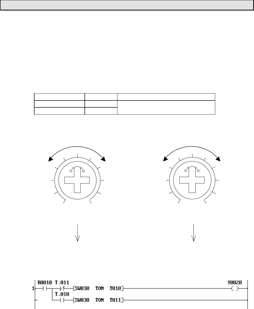
6F3B0253
270 T1-16S User’s Manual
8. Special I/O Functions
8.5 Analog setting function
Function
The value of the analog setting adjuster is converted into a digital value (0 to 1000)
and stored in the SW register. 2 adjusters are provided. (V0 and V1)
The SW register data can be used as timer presets or any parameters for function
instructions.
Related registers
Function Register Remarks
Adjuster V0 SW30 Data range: 0 to 1000
Adjuster V1 SW31
Operation
V0 V1
SW30 (0 to 1000) SW31 (0 to 1000)
Sample program
The above example is a simple flicker circuit of Y020. In this example, the ON/OFF
interval of Y020 can be controlled by the adjuster V0.
Decrease Increase Decrease Increase

6F3B0253
Basic Hardware and Function 271
8. Special I/O Functions
8.6 Pulse output function
Function
This function is used to output a variable frequency pulse train. The controllable pulse
frequency is 50 to 5000 Hz (1 Hz units).
The output mode can be selected either CW/CCW or Pulse/Direction (PLS/DIR).
In the CW/CCW mode, CW pulse is output when the frequency setting is positive (50
to 5000), and CCW pulse is output when it is negative (-50 to -5000).
In the PLS/DIR mode, DIR is OFF when the frequency setting is positive (50 to 5000),
and DIR is ON when it is negative (-50 to -5000).
< CW/CCW mode > CW
CCW
< PLS/DIR mode > PLS
DIR
In the both modes, pulse output is enabled when the pulse enable flag is ON. While
the pulse enable flag is ON, the pulse frequency can be changed by changing the
frequency setting value. However, the pulse direction (the sign of the frequency
setting) cannot be changed when the pulse enable flag is ON.
This function can be used to control the speed of a stepping motor, etc.
Related registers
SW26: Function selection. Refer to section 8.1.
Function Register/ Remarks
CW/CCW PLS/DIR device
CW pulse PLS Y020
CCW pulse DIR Y021
Pulse enable flag S270 Output is enabled when ON
Frequency setting register SW28 Data range: -5000 to -50, 50 to 5000
Frequency setting error flag S26F ON at error (reset OFF automatically)
Note) The allowable value range of the frequency setting (SW28) is -5000 to -50 and
50 to 5000. If the value is out of this range or the sign is changed while the
pulse enable flag (S270) is ON, the frequency setting error flag (S26F) comes
ON. (Pulse output operation is continued with previous frequency setting)
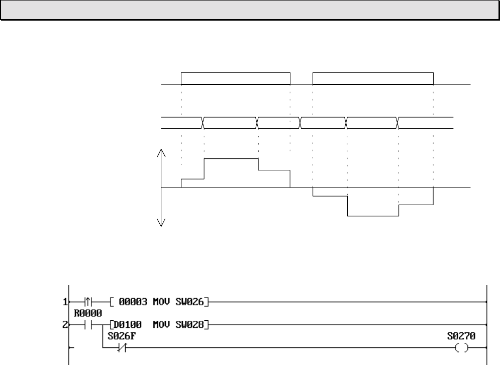
6F3B0253
272 T1-16S User’s Manual
8. Special I/O Functions
Operation
Pulse enable
Frequency setting
+
Frequency
Pulse output
-
Sample program
In this example, 3 (H0003) is set in SW26. As a result, the CW/CCW mode pulse
output function is selected.
When R000 is ON, the pulse output is started with the frequency designated by
D0100.
If an invalid frequency is designated, the frequency setting error flag (S26F) comes
ON and the pulse enable flag (S270) is turned OFF. Then the pulse output is stopped.
-300-1000
3001000
100 -100
1KHz 300Hz
100Hz
300Hz
100Hz
1KHz
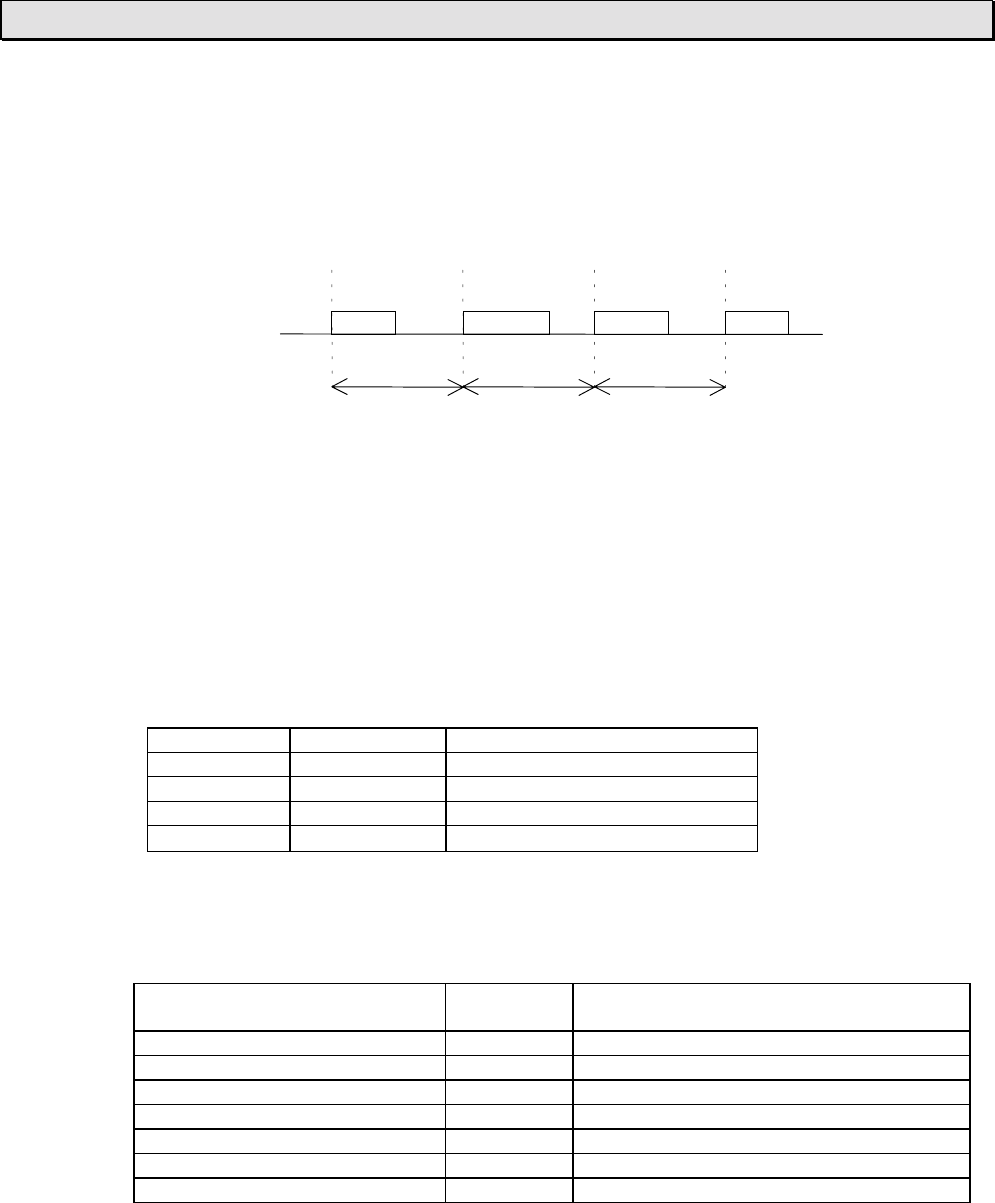
6F3B0253
Basic Hardware and Function 273
8. Special I/O Functions
8.7 PWM output function
Function
This function is used to output a variable duty cycle pulse train. The controllable duty
cycle is 0 to 100 % (1 % units).
ON duty 50% 70% 60%
PWM
T T T T = Pulse cycle
The PWM output is enabled when the pulse enable flag is ON. While the pulse enable
flag is ON, the duty cycle (ON duty) can be changed by changing the duty setting
value (0 to 100).
The frequency setting is available in the range of 50 to 5000 Hz (1 Hz units) before
turning ON the pulse enable flag. The frequency changing is not allowed while the
pulse enable is ON.
Note that the minimum ON/OFF pulse duration is 100 µs. Therefore, the controllable
ON duty range is limited depending on the frequency setting as follows. If the ON duty
setting value is not available (within 0 to 100), the pulse width error flag comes ON.
(PWM output operation is continued but the duty cycle is not guaranteed)
Frequency Cycle time Available ON duty
50 - 100 Hz 20 - 10 ms 0 to 100 %
200 Hz 5 ms 0, 2 to 98, 100 %
1000 Hz 1 ms 0, 10 to 90, 100 %
5000 Hz 200 µs0, 50, 100 %
Related registers
SW26: Function selection. Refer to section 8.1.
Function Register/
device Remarks
PWM pulse Y020
Pulse enable flag S270 Output is enabled when ON
Frequency setting register SW28 Data range: 50 to 5000
ON duty setting register SW29 Data range: 0 to 100
Pulse width error flag S26D ON at error (reset OFF automatically)
ON duty setting error flag S26E ON at error (reset OFF automatically)
Frequency setting error flag S26F ON at error (reset OFF automatically)
Note) If the setting value of SW28 or SW29 is out of the allowable range, the
frequency setting error flag (S26F) or the ON duty setting error flag (S26E)
comes ON. (PWM output operation is continued with previous ON duty setting)
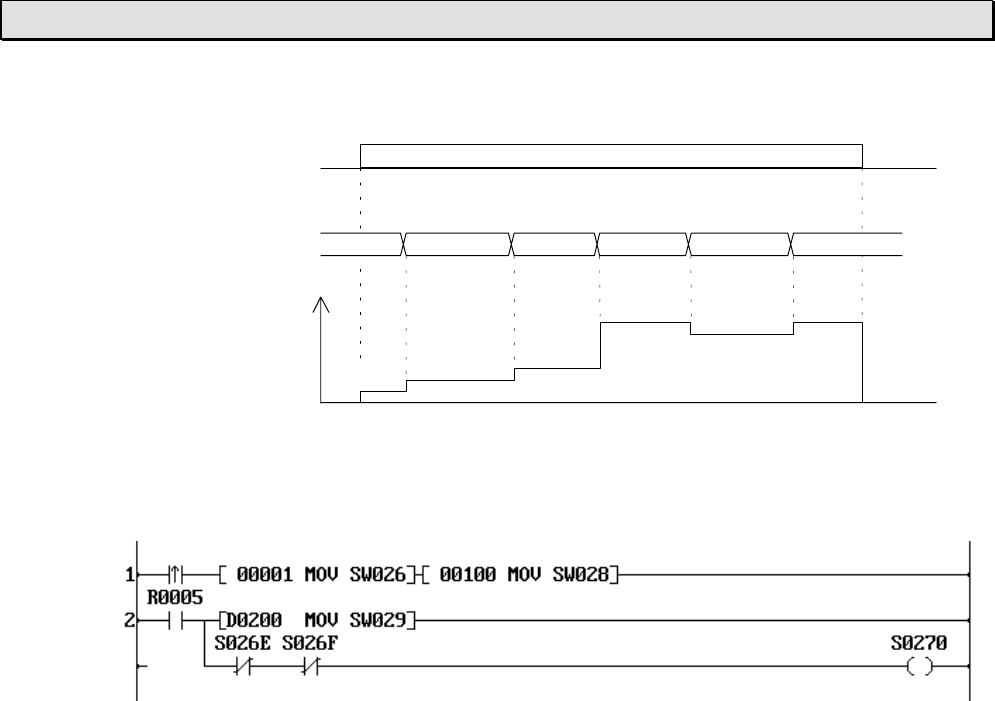
6F3B0253
274 T1-16S User’s Manual
8. Special I/O Functions
Operation
Pulse enable
ON duty setting
ON duty
PWM output
Sample program
In this example, 1 (H0001) is set in SW26 and 100 is set in SW28. As a result, 100 Hz
PWM output function is selected.
When R005 is ON, the PWM output is started with the duty cycle designated by
D0200.
If an invalid ON duty is designated, the ON duty setting error flag (S26E) comes ON
and the pulse enable flag (S270) is turned OFF. Then the PWM output is stopped.
70
6070
302010
70%
60%
70%
30%
20%
10%

6F3B0253
Basic Hardware and Function 275
Section 9
Maintenance and Checks
9.1 Precautions during operation, 276
9.2 Daily checks, 277
9.3 Periodic checks, 278
9.4 Maintenance parts, 279
9.5 Battery, 280

6F3B0253
276 T1-16S User’s Manual
9. Maintenance and Checks
9.1 Precautions during operation
When the T1-16S is in operation, you should pay attention to the following items.
(1) The programmer cable can be plugged or unplugged while the T1-16S is in
operation. When you try to do it, do not touch the connector pins. This may cause
malfunction of the T1-16S owing to static electricity.
(2) Do not plug nor unplug the expansion cable during power on. This can cause
damage to the equipment. Furthermore, to avoid malfunction of the T1-16S owing
to static electricity, do not touch the cable ends.
(3) Do not touch any terminals while the T1-16S is in operation, even if the terminals
are not live parts. This may cause malfunction of the T1-16S owing to static
electricity.
(4) Do not touch the expansion connector pins while the T1-16S is in operation. This
may cause malfunction of the T1-16S owing to static electricity.
Fix the expansion connector cover if the expansion connector is not used.
(5) Turn off power when a battery installs and removes.

6F3B0253
Basic Hardware and Function 277
9. Maintenance and Checks
9.2 Daily checks
To maintain the system and to prevent troubles, check the following items on daily
basis.
Item Check Corrective measures
PWR
(power) Lit when internal 5V is
normal.
RUN Lit when operating
normally.
Status LEDs
FLT (fault) Not lit when operating
normally.
If the LEDs are not normal, see
10. Troubleshooting.
Mode control
switch Check that the mode control switch is
in R (RUN) side. Normal operation is
performed when this switch is in R
(RUN) side.
Turn this switch to R (RUN) side.
Input LEDs Lit when the corresponding input is
ON. • Check that the input terminal
screw is not loose.
• Check that the input terminal
block is not loose.
• Check that the input voltage is
within the specified range.
Output LEDs Lit when the output is ON and the
corresponding load should operate. • Check that the output terminal
screw is not loose.
• Check that the output terminal
block is not loose.
• Check that the output voltage
is within the specified range.
!CAUTION 1. Pay special attention during the maintenance work to minimize the risk
of electrical shock.
2. Turn off power immediately if the T1-16S or related equipment is
emitting smoke or odor. Operation under such situation can cause fire
or electrical shock.

6F3B0253
278 T1-16S User’s Manual
9. Maintenance and Checks
9.3 Periodic checks
Check the T1-16S based on the following items every six months. Also perform
checks when the operating environment is changed.
Item Check Criteria
Measure the power voltage at the T1-
16S’s power terminals. 85 - 132/170 - 264Vac (AC PS)
20.4 - 28.8Vdc (DC PS)
Check that the terminal screw is not
loose. Not loose
Power supply
Check that the power cable is not
damaged. Not damaged
Check that the unit is installed
securely. Not loose, no play
Check that the I/O module is inserted
securely. (if any) Not loose, no play
Check that the expansion rack/unit is
installed securely. (if any) Not loose, no play
Check that the expansion cable is
connected securely and the cable is
not damaged. (if any)
Not loose, not damaged
Installation
condition
Check that the I/O module on the
expansion rack is inserted securely. (if
any)
Not loose, no play
Measure the input/output voltage at
the T1-16S’s terminals. The voltage must be within the
specified range.
Check the input status LEDs. The LED must light normally.
Check the output status LEDs. The LED must light normally.
Check that the terminal block is
installed securely. Not loose, no play
Check that the terminal screw is not
loose and the terminal has a sufficient
distance to the next terminal.
Not loose, not contacting the
next terminal
Input/output
Check that the each I/O wire is not
damaged. Not damaged
!CAUTION 1. Pay special attention during the maintenance work to minimize the risk
of electrical shock.
2. Turn off power immediately if the T1-16S or related equipment is
emitting smoke or odor. Operation under such situation can cause fire
or electrical shock.
6F3B0253
Basic Hardware and Function 279
9. Maintenance and Checks
(Periodic checks - continued)
Item Check Criteria
Environment Check that the temperature, humidity,
vibration, dust, etc. are within the
specified range.
Must be within the range of
general specification.
Check that the functions of the
programming tool are normal. Monitoring and other operations
are available.
Programming tool
Check that the connector and cable
are not damaged. Not damaged
User program Check that the T1-16S program and
the master program (saved on a floppy
disk, etc.) are the same.
No compare error
9.4 Maintenance parts
To recover from trouble quickly, it is recommended to keep the following spare parts.
Item Quantity Remarks
T1-16S basic unit 1 Prepare at least one to minimize the down-time
of the controlled system.
Programming tool 1 Useful for the troubleshooting procedure.
Master program As required Saved on a floppy disk, etc.
Expansion rack or
unit (if any) 1
I/O module
(if any) One of each type
used
Fuse for I/O
module (if any) One of each type
used
Battery (CR2032) 1
These spare parts should not be stored in high temperature and/or humidity locations.
6F3B0253
280 T1-16S User’s Manual
9. Maintenance and Checks
9.5 Battery
(1) Install
Insert the battery by an angle of 45°.
(Turn + side into an upside.)
(1) Push the battery horizontal direction.
(2) Push from upside and lock.
(2) Eject
Push the center of the tab by a finger or a pen. Then
the battery will be unlocked.
Remove the battery.
1. Turn off power when installing or removing the battery for safety.
2. The battery type is CR2032. Do not use other types of battery. Use of
another battery may present a risk of fire or explosion.
3. Dispose of used battery promptly. Keep away from children. Do not
disassemble and do not dispose of in fire.
NOTE
+ side

6F3B0253
Basic Hardware and Function 281
Section 10
Troubleshooting
10.1 Troubleshooting procedure, 282
10.2 Self-diagnostic items, 288
6F3B0253
282 T1-16S User’s Manual
10. Troubleshooting
10.1 Troubleshooting procedure
If a trouble occurs, determine whether the cause lies in the mechanical side or in the
control system (PLC) side. A problem may cause a secondary problem, therefore, try
to determine the cause of trouble by considering the whole system.
If the problem is found in the T1-16S, check the following points:
PWR (power) LED Follow the procedure in
10.1.1 Power supply check
Lit
RUN LED Follow the procedure in
10.1.2 CPU check
Lit
User program Follow the procedure in
10.1.3 Program check
Normal operation
Input operation Follow the procedure in
10.1.4 Input check
Normal operation
Output operation Follow the procedure in
10.1.5 Output check
Also refer to section 10.1.6 for environmental problem.
!CAUTION 1. Pay special attention during the troubleshooting to minimize the risk of
electrical shock.
2. Turn off power immediately if the T1-16S or related equipment is
emitting smoke or odor. Operation under such situation can cause fire
or electrical shock.
3. Turn off power before removing or replacing units, modules, terminal
blocks or wires. Failure to do so can cause electrical shock or damage
to the T1 and related equipment.
4. Contact Toshiba for repairing if the T1-16S or related equipment is
failed. Toshiba will not guarantee proper operation nor safety for
unauthorized repairing.
Not lit
Not lit
Not normal
Not normal
Not normal
6F3B0253
Basic Hardware and Function 283
10. Troubleshooting
10.1.1 Power supply check
If the PWR (power) LED is not lit after power on, check the following points.
Check the power connection Connection terminals are correct.
The terminal screws are not loose.
The terminal block is installed securely.
Correct
Check the power voltage 85 to 132/170 to 264Vac (50/60 Hz)
at the T1-16S’s terminal or 20.4 to 28.8Vdc (DC power)
Normal
Remove the programmer If the PWR LED becomes normal, the
port connector internal 5Vdc can be shorted in the
external connections of this port.
Still unlit
Remove the 24Vdc service If the PWR LED becomes normal, the
power terminals if it is used 24Vdc service power can be over load.
Still unlit
Remove the I/O modules. If the PWR LED is still unlit, the T1-16S
basic unit may be faulty. Replace the unit.
Lit
Confirm the internal 5Vdc The 5Vdc capacity for I/O modules is
current consumption if max. 1.5A.
I/O module is used. (Refer to section 2.1.)
Within the limit
Insert the removed option Replace the faulty I/O module.
modules one by one to
pinpoint the faulty card.
6F3B0253
284 T1-16S User’s Manual
10. Troubleshooting
10.1.2 CPU check
If the PWR (power) LED is lit but the RUN LED is not lit, check the following points.
Check the position of the If it is not in R (RUN) position, turn the
mode control switch switch to R (RUN) position.
Check the FLT (fault) LED If the FLT LED is lit or blinking, the T1-16S
is in the ERROR mode. Confirm the error
message by connecting the
programming tool. Refer to section 10.2.
Is the RUN LED blinking ? If it is blinking, the T1-16S is in the HOLD
mode. Check your program
whether the HOLD device (S401) is
not used.
Connect the programming If the T1-16S stays in HALT mode even
tool, and check the T1-16S’s when the mode control switch is changed,
status the switch may be faulty.
If the communication between the T1-16S
and the programming tool is not possible,
the T1-16S may be faulty.
10.1.3 Program check
Check the user program based on the following points if it is running but the operation
does not work as intended.
(1) Whether duplicated coils are not programmed.
(2) Whether a coil device and a destination of a function instruction are not
overlapping.
(3) Whether the ON/OFF duration of an external input signal is not shorter than the
T1-16S’s scan time.
(4) Whether a register/device, which is used in the main program, is not operated
erroneously in the interrupt program.
When you write/modify the program, it is necessary to execute the
EEPROM write operation before turning off power to the T1. Otherwise the
old program stored in the built-in EEPROM will be over-written, and your
program modification will disappear.
NOTE
6F3B0253
Basic Hardware and Function 285
10. Troubleshooting
10.1.4 Input check
If the program is running but the external input signal is not read normally, check the
following points:
Is the input status LED If not, check the input voltage at the
changed ON/OFF according T1-16S’s input terminals.
to the corresponding input If the voltage is not normal, check the input
device operation ? device and the cable.
If the voltage is normal, the T1-16S’s input
Yes circuit may be faulty.
Connect the programming If the monitored X device state is identical
tool, and monitor the to the state of the input status LED, the
corresponding X device state cause may lie in the user program or in the
in RUN mode environment.
Not normal
Check whether the X device If it is forced, release the force designation
is forced or not then execute the EEPROM write
operation.
Not forced
Check whether the I/O If identical, the T1-16S’s internal circuit or
allocation table is identical to the input circuit may be faulty.
the actual I/O configuration
Not identical
Execute the automatic I/O If it becomes identical, execute the
allocation, and check whether EEPROM write operation.
the I/O allocation table is now
identical to the actual I/O
configuration
Still not identical
Is the allocation mismatch for If so, the card, module or expansion unit
a specific I/O module? may be faulty. For expansion unit, check
the expansion cable also.
6F3B0253
286 T1-16S User’s Manual
10. Troubleshooting
10.1.5 Output check
If the output status monitored on the programming tool is normal but the external
output device (load) is not operated normally, check the following points:
Is the output status LED
changed ON/OFF according
No to the program execution ?
Yes
Check the voltage between If it is the circuit voltage at the output is
the output terminal and its ON, or if it is 0V at the output is OFF with
common terminal. the load ON, the T1-16S’s output circuit
It should be 0V when the may be faulty.
output is ON, and it should If it is 0V and the load is also OFF, check
be the circuit voltage when the output power and the output cable
the output is OFF. connections.
Normal If it is not normal, check the output cable
Check the voltage at the load connections.
If it is normal, check the specification of
the load, also check environmental factors.
Check whether the I/O If identical, the T1-16S’s internal circuit or
allocation table is identical to the output circuit may be faulty.
the actual I/O configuration
Not identical
Execute the automatic I/O If it becomes identical, execute the
allocation, and check whether EEPROM write operation.
the I/O allocation table is now
identical to the actual I/O
configuration
Still not identical
Is the allocation mismatch for If so, the card, module or expansion unit
a specific I/O module? may be faulty. For expansion unit, check
the expansion cable also.

6F3B0253
Basic Hardware and Function 287
10. Troubleshooting
10.1.6 Environmental problem
If the following improper operations occur in the controlled system, check possible
environmental factors.
(1) If an improper operation occurs synchronously with the operation of I/O devices:
The noise generated at ON/OFF of the output device (load) may be the cause of
the problem. Take necessary measures mentioned in section 3.
(2) If an improper operation occurs synchronously with the operation of surrounding
equipment or high-frequency equipment:
The noise induced in I/O signal lines may be the cause of the problem. The surge
voltage, voltage fluctuations, or differences of grounding potentials may cause
the problem, depending on the power supply system or the grounding system.
Check the operation in accordance with the precautions in section 4. For some
cases, isolation from the ground may lead to the stable operation.
(3) If an improper operation occurs synchronously with the operation of machinery:
The vibration of the equipment may cause the problem. Check that the installation
status of the units and take necessary measures.
(4) If a similar failure is repeated after the unit is replaced:
Check that no metal debris or water drops has been entered into the unit/module.
Apart from the above points, consider climatic conditions. If the ambient temperature
is beyond the specified range, stable operation of the system is not guaranteed.

6F3B0253
288 T1-16S User’s Manual
10. Troubleshooting
10.2 Self-diagnostic items
If an error is detected by the self-diagnostic check of the T1-16S CPU, the error
messages and the related information shown on the following pages will be recorded
in the T1-16S’s event history table. If the error is severe and continuation of operation
is not possible, the T1-16S turns OFF all outputs and stops the operation (ERROR
mode).
The latest 15 error messages are stored in the event history table. This event history
table can be displayed on the programming tool. (Power ON/OFF is also registered)
If the T1-16S has entered into ERROR mode, connect the programming tool to the T1-
16S to confirm the error message in the event history table. This information is
important to recover from a trouble. For the key operations on the programming tool to
display the event history table, refer to the separate manual for the programming tool.
(An example of the event history)
< Event History>
Date Time Event Count Info 1 Info 2 Info 3 Mode
1. 98-02-21 16:48:01 I/O no answer 3 #00-04 RUN Down
2. 98-02-21 15:55:26 System power on 1 INIT.
3. 98-02-21 12:03:34 System power off 1 RUN
4. 98-01-15 09:27:12 System power on 1 INIT.
5. 98-01-14 19:11:43 System power off 1 HALT
6. 98-01-14 10:39:11 No END/IRET error 3 M-001 H0024 HALT Down
In the event history table, No.1 message indicates the latest event recorded.
Each column shows the following information.
Date: The date when the error has detected (Enhanced model only)
Time: The time when the error has detected (Enhanced model only)
Event: Error message
Count: Number of times the error has detected by retry action
Info n: Related information to the error detected
Mode: T1-16S’s operation mode in which the error has detected (INIT. means the
power-up initialization)
Down: Shows the T1-16S has entered into ERROR mode by the error detected
If the T1-16S is in the ERROR mode, operations to correct the program are not
accepted.
In this case, execute the Error reset operation by the programming tool to return the
HALT mode before starting the correction operation.

6F3B0253
Basic Hardware and Function 289
10. Troubleshooting
Error message and related information Special Meaning and countermeasures
Event Info 1 Info 2 Info 3 device
Batt voltage drop S00F In the power-up initialization, data invalidity
of RAM (back-up area) has been detected.
If retentive registers are used, these validity
are not guaranteed. (No error down)
Boundary error Program
type - Address
in the FUN No. The register of index modification is other
than RW, T, C and D. (Error down)
block No. block S064 The register designated by index
modification has exceeded the allowable
range. That is, out of RW, T, C and D.
(No error down)
Check the value of the index register.
Clock-calendar error S00A The data of built-in calendar LSI is illegal.
(No error down)
Set the date and time.
(Enhanced model only)
Duplicate entry No. Program
type -
block No.
Address
in the
block
Entry No. Multiple SUBR instructions which have the
same subroutine number are programmed.
(Error down)
Check the program.
EEPROM BCC error Illegal
BCC S004
S013 BCC error has been detected in the user
program of the EEPROM. (Error down)
Reload the program and execute EEPROM
write operation again.
EEPROM warning Number
of excess
writing
S007 The number of times of writing into
EEPROM has exceeded the life (100,000
times). (No error down)
Replace the unit because the data reliability
of the EEPROM will decrease.
I/O bus error Unit No. Data S005
S020 An abnormality has been detected in I/O
bus checking. (Error down)
Check the expansion cable connection and
I/O module mounting status.
I/O mismatch Unit No. -
slot No. Register
No. S005
S021 The I/O allocation information and the
actual I/O configuration are not identical.
(Error down)
Check the I/O allocation and the I/O module
mounting status.
I/O no answer Unit No. -
slot No. Register
No. S005
S022 No response from the T2 I/O module has
been received. (Error down)
Check the I/O allocation, the expansion
cable connection and the T2 I/O module
mounting status.
I/O parity error Unit No. -
slot No. Register
No. S005
S023 I/O bus parity error has been detected in
data read/write for T2 I/O modules. (Error
down)
Check the expansion cable connection and
the T2 I/O module mounting status.
Illegal I/O reg Unit No. -
slot No. Register
No. S005
S021 The allocated I/O register address exceeds
the limit, 32 words. (Error down)
Check the I/O allocation.

6F3B0253
290 T1-16S User’s Manual
10. Troubleshooting
Error message and related information Special Meaning and countermeasures
Event Info 1 Info 2 Info 3 device
Illegal inst Program
type -
block No.
Address
in the
block
S006
S030
S060
An illegal instruction has been detected in
the program. (Error down)
Reload the program and execute EEPROM
write operation again.
Illegal sys intrpt Interrupt
address 1 Interrupt
address 2 Unregistered interrupt has occurred. (No
error down)
If the error occurs frequently, replace the
unit.
Invalid Fun inst Program
type -
block No.
Address
in the
block
Fun No. A function instruction which is not supported
by the T1-16S is programmed. (Error down)
Correct the program.
Invalid program Program
type -
block No.
A basic ladder instruction which is not
supported by the T1-16S is programmed.
(Error down)
Correct the program.
SUBR instruction is not programmed before
RET instruction. (Error down)
Correct the program.
An abnormality is detected in the program
management information. (Error down)
Reload the program and execute EEPROM
write operation again.
Loop nesting error Program
type -
block No.
Address
in the
block
A FOR-NEXT loop is programmed inside
other FOR-NEXT loop. (Error down)
Correct the program.
Memory full The program exceeds the executable
memory capacity. (Error down)
Reduce the program steps.
No END/IRET error Program
type -
block No.
Address
in the
block
The END instruction is not programmed in
the main program or in the sub-program.
(Error down)
Correct the program.
The IRET instruction is not programmed in
the interrupt program. (Error down)
Correct the program.
No RET error Program
type -
block No.
Address
in the
block
Sub-r No. The RET instruction is not programmed in
the subroutine program. (Error down)
Correct the program.
No sub-r entry Program
type -
block No.
Address
in the
block
Sub-r No. The subroutine corresponding to CALL
instruction is not programmed. (Error down)
Correct the program.

6F3B0253
Basic Hardware and Function 291
10. Troubleshooting
Error message and related information Special Meaning and countermeasures
Event Info 1 Info 2 Info 3 device
Operand error Program
type -
block No.
Address
in the
block
A register/device which is not supported by
the T1-16S is programmed. (Error down)
Correct the program.
The timer or counter register is duplicated in
the program. (Error down)
Correct the program.
The subroutine number programmed with
CALL or SUBR instruction is out of the
range. (Error down)
0 to 255
Correct the program.
Index modification is programmed for
instructions in which the index modification
is not allowed. (Error down)
Correct the program.
Pair inst error Program
type -
block No.
Address
in the
block
The combination is illegal for MCS-MCR,
JCS-JCR or FOR-NEXT instructions. (Error
down)
Correct the program.
A MCS-MCR is programmed inside other
MCS-MCR segment. (Error down )
Correct the program.
A JCS-JCR is programmed inside other
JCS-JCR segment. (Error down )
Correct the program.
Peripheral LSI err Error
code S004
S016 CPU hardware error has been detected in
the power-up initialization. (Error down and
programming tool cannot be connected)
Replace the unit if the error remains after
power OFF and ON again.
Program BCC error Illegal
BCC S006
S030 BCC error has been detected in the user
program in the RAM. (Error down)
If the error remains after power OFF and
ON again, reload the program and execute
EEPROM write operation.
RAM check error Error
address Error data Test data S004
S012 In the power-up initialization, an error has
detected by RAM read/write checking. (Error
down)
Replace the unit if the error remains after
power OFF and ON again.
Scan time over Scan time S006
S031 The scan time has exceeded 200 ms. (Error
down)
Correct the program to reduce the scan time
or use WDT instruction to extend the check
time.

6F3B0253
292 T1-16S User’s Manual
10. Troubleshooting
Error message and related information Special Meaning and countermeasures
Event Info 1 Info 2 Info 3 device
Sys RAM check err Error
address Error data Test data S004
S011 In the power-up initialization, an error has
detected by system RAM read/write
checking. (Error down and programming
tool cannot be connected)
Replace the unit if the error remains after
power OFF and ON again.
Sys ROM BCC error Illegal
BCC S004
S010 BCC error has been detected in the system
program in the ROM. (Error down and
programming tool cannot be connected)
Replace the unit if the error remains after
power OFF and ON again.
System power off Power OFF (no error)
System power on Power ON (no error)
Sub-r nesting err Program
type -
block No.
Address
in the
block
Sub-r No. The nesting of subroutines exceeds 3
levels.
(Error down)
Correct the program.
WD timer error Address 1 Address 2 S004
S01F The watchdog timer error has occurred.
(Error down)
If the error occurs frequently, replace the
unit.

6F3B0253
Basic Hardware and Function 293
Appendix
A.1 List of models and types, 294
A.2 Instruction index, 295

6F3B0253
294 T1-16S User’s Manual
Appendix
A.1 List of models and types
• Basic unit
Model Power supply Input type RTC/RS-485 Type code Part number
Yes T1-MDR16SS TDR116S6S100 – 240Vac
No T1-MDR16SC TDR116S6C
Yes T1-MDR16SSD TDR116S3S
T1-16S
24Vdc
24Vdc
No T1-MDR16SCD TDR116S3C
• I/O module
Description Type code Part number
16 points 24Vdc input DI116M TDI116M∗S
16 points 24Vdc output DO116M TDO116M∗S
8 points 24Vdc input and 8 points 24Vdc output DD116M TDD116M∗S
8 points relay output RO108M TRO108M∗S
1 channel analog input, 0 – 5V/0 - 20mA AD121M TAD121M∗S
1 channel analog input, ±10V AD131M TAD131M∗S
1 channel analog output, 0 – 20mA DA121M TDA121M∗S
1 channel analog output, ±10V DA131M TDA131M∗S
1 channel thermo couple input, K/E/J TC111M TTC111M∗S
TOSLINE-F10 remote station FR112M TFR112M∗S
• Peripherals
Description Type code Part number
Handy programmer (with 2 m cable for T1/T1S) HP911A THP911A∗S
T-PDS software (Windows version) T-PDS Windows TMW33E2SS
Program storage module RM102 TRM102∗∗S
Multi-drop adapter for computer link CU111 TCU111∗∗S
• Cable and others
Description Type code Part number
T-PDS cable for T1/T1S, 5m length CJ105 TCJ105∗CS
HP911A cable for T1/T1S, 2m length (spare parts) CJ102 TCJ102∗CS
RS-232C connector for computer link
(with 2 m cable) PT16S TPT16S∗AS
I/O module I/O connector for
DI116M/DO116M/DD116M, soldering type PT15S TPT15S∗AS
I/O module I/O connector for
DI116M/DO116M/DD116M, flat cable type PT15F TPT15F∗AS

6F3B0253
Basic Hardware and Function 295
Appendix
A.2 Instruction index
• Instruction name
1 bit rotate left 173 Exclusive OR 158
1 bit rotate right 172 Expanded data transfer 241
1 bit shift left 165 Flip-flop 215
1 bit shift right 164 FOR 205
2’s complement 232 Forced coil 122
7-segment decode 234 Function generator 229
Absolute value 231 Greater than 178
Addition 143 Greater than or equal 179
Addition with carry 149 Hex to ASCII conversion 161
AND 156 Increment 154
ASCII conversion 236 Interrupt return 210
ASCII to Hex conversion 162 Invert coil 124
Average value 228 Invert transfer 138
BCD conversion 238 Inverter 123
Bi-directional shift register 170 Jump control reset 134
Binary conversion 237 Jump control set 134
Bit count 202 Less than 182
Bit test 163 Less than or equal 183
Calendar operation 218 Lower limit 225
Coil 121 Master control reset 133
Counter 132 Master control set 133
Data exchange 139 Maximum value 226
Data transfer 136 Minimum value 227
Decode 201 Moving average 159
Decrement 155 Multiplexer 176
Demultiplexer 177 Multiplication 145
Device/register reset 197 n bit rotate left 175
Device/register set 196 n bit rotate right 174
Digital filter 160 n bit shift left 167
Direct I/O 239 n bit shift right 166
Disable interrupt 209 NC contact 118
Division 146 Negative pulse coil 128
Double-word 2’s complement 233 Negative pulse contact 126
Double-word addition 147 NEXT 206
Double-word data transfer 137 NO contact 117
Double-word equal 286 Not equal 181
Double-word greater than 284 OFF delay timer 130
Double-word greater than or equal 285 ON delay timer 129
Double-word less than 288 OR 157
Double-word less than or equal 289 Positive pulse coil 127
Double-word not equal 287 Positive pulse contact 125
Double-word subtraction 148 Pre-derivative real PID 219
Enable interrupt 208 Reset carry 199
Encode 200 Set calendar 217
End 135 Set carry 198
Equal 180 Shift register 168

6F3B0253
296 T1-16S User’s Manual
Appendix
Single shot timer 131
Special module data read 245
Special module data write 247
Step sequence initialize 212
Step sequence input 213
Step sequence output 214
Subroutine call 203
Subroutine entry 207
Subroutine return 204
Subtraction 144
Subtraction with carry 150
Table initialize 140
Table invert transfer 142
Table transfer 141
Transitional contact (falling) 120
Transitional contact (rising) 119
Unsigned division 152
Unsigned double/single division 153
Unsigned equal 192
Unsigned greater than 190
Unsigned greater than or equal 191
Unsigned less than 194
Unsigned less than or equal 195
Unsigned multiplication 151
Unsigned not equal 193
Up-down counter 216
Upper limit 224
Watchdog timer reset 211

6F3B0253
Basic Hardware and Function 297
Appendix
• Instruction symbol
∗145 FG 229 U/D 216
+ 143 FOR 205 U< 194
+1 154 HTOA 161 U<= 195
+C 149 I/O 239 U<> 193
- 144 IRET 210 U= 192
-1 155 JCR 134 U> 190
-C 150 JCS 134 U>= 191
/ 146 LL 225 UL 224
< 182 MAVE 159 WDT 211
<= 183 MAX 226 WRITE 247
<> 181 MCR 133 XCHG 139
= 180 MCS 133 XFER 241
> 178 MIN 227
>= 179 MOV 136
7SEG 234 MPX 176
ABS 231 NEG 232
AND 156 NEXT 206
ASC 236 NOT 138
ATOH 162 OR 157
AVE 228 PID3 219
BC 202 READ 245
BCD 238 RET 204
BIN 237 RST 197
CALL 203 RSTC 199
CLDN 217 RTL 175
CLDS 218 RTL1 173
CNT 132 RTR 174
D+ 147 RTR1 172
D- 148 SET 196
D< 188 SETC 198
D<= 189 SHL 167
D<> 187 SHL1 165
D= 186 SHR 166
D> 184 SHR1 164
D>= 185 SR 168
DEC 201 SS 131
DFL 160 STIN 213
DI 209 STIZ 212
DIV 153 STOT 214
DMOV 137 SUBR 207
DNEG 233 TEST 163
DPX 177 TINZ 140
DSR 170 TMOV 141
EI 208 TNOT 142
ENC 200 TOF 130
END 135 TON 129
EOR 158 U∗151
F/F 215 U/ 152
6F3B0253
298 T1-16S User’s Manual

TOSHIBA CORPORATION
Industrial Equipment Department
1-1, Shibaura 1-chome, Minato-ku
Tokyo 105-8001, JAPAN
Tel: 03-3457-4900 Fax: 03-5444-9268
