Toshiba Tw40F80 Technical Training Manual Toc
TW40F80 to the manual 9d699d9e-c699-44ff-a762-9b3b908906d0
2014-12-13
: Toshiba Toshiba-Tw40F80-Technical-Training-Manual-131341 toshiba-tw40f80-technical-training-manual-131341 toshiba pdf
Open the PDF directly: View PDF ![]() .
.
Page Count: 101 [warning: Documents this large are best viewed by clicking the View PDF Link!]
- Contents
- Section I: Outline 6
- 1. FEATURE 6
- 2. MERITS OF BUS SYSTEM
- 3. SPECIFICATIONS 7
- 4. FRONT VIEW 8
- 5. Rear View
- 6. Remote Control View
- 7. CHASSIS LAYOUT
- 8. CONSTRUCTION OF CHASSIS 12
- section ii: tuner, if/mts/s. pro module
- 1. CIRCUIT BLOCK
- 2. PoP TUNER
- section iii: channel selection circuit
- 1. OUTLINE OF CHANNEL SELECTION CIRCUIT SYSTEM
- 2. OPERATION OF CHANNEL SELECTION CIRCUIT
- 3. MICROCOMPUTER
- 4. MICROCOMPUTER TERMINAL FUNCTION
- 5. EEPROM (QA02)
- 6. ON SCREEN FUNCTION
- 7. SYSTEM BLOCK DIAGRAM
- 8. LOCAL KEY DETECTION METHOD
- 9. REMOTE CONTROL CODE ASSIGNMENT
- 10. ENTERING TO SERVICE MODE
- 11. TEST SIGNAL SELECTION
- 12. SERVICE ADJUSTMENT
- 13. FAILURE DIAGNOSIS PROCEDURE
- 14. TROUBLESHOOTING CHART
- section iv: dvd switch circuit
- 1. dvd switch block diagram
- 2. OUTLINE
- section v: wac circuit
- 1. outline
- 2. CIRCUIT OPERATION
- 3. BLOCK DIAGRAM
- 4. WIDE ASPECT CONVERSION CIRCUIT FAILURE ANALYSIS PROCEDURES
- section vi: dual circuit
- 1. Outline
- 2. Principles of Operation
- 3. SYSTEM COMPONENT DIAGRAM OF DUAL UNIT
- 4. Circuit Operation
- 5. TERMINAL FUNCTION, DESCRIPTION AND BLOCK DIAGRAM OF Main IC
- section vii: 3-dimension y/c separator circuit
- 1. outline
- 2. CIRCUIT DESCRIPTION
- section viii: vertical output circuit
- 1. OUTLINE
- 2. V OUTPUT CIRCUIT
- 3. Protection Circuit for V Deflection Stop
- 4. RASTER POSITION SWITCHING CIRCUIT
- section ix: horizontal deflection circuit
- 1. OUTLINE
- 2. HORIZONTAL DRIVE CIRCUIT
- 3. BASIC OPERATION OF HORIZONTAL DRIVE
- 4. HORIZONTAL OUTPUT CIRCUIT
- 5. HIGH VOLTAGE GENERATION CIRCUIT
- 6. High Voltage Circuit
- 7. X-RAY PROTECTION CIRCUIT
- 8. OVER CURRENT PROTECTION CIRCUIT
- section x: deflection distortion correction circuit
- (side dpc circuit)
- 1. DEFLECTION DISTORTION CORRECTION IC (TA8859CP)
- 2. DIODE MODULATOR CIRCUIT
- 3. ACTUAL CIRCUIT
- section xi: digital convergence circuit
- 1. OUTLINE
- 2. CIRCUIT DESCRIPTION
- 3. PICTURE ADJUSTMENT
- 4. Case study
- 5. TROUBLESHOOTING
- 6. CONVERGENCE OUTPUT CIRCUIT
- 7. Convergence troubleshooting chart

TECHNICAL TRAINING MANUAL
N5SS CHASSIS
NTDPJTV05
TW40F80
PROJECTION TELEVISION
Only the different points from the training manual “N5SS chassis” with its file
No. 026-9506 are described on this manual.
For other parts common with “N5SS chassis”, please refer to the original manual
with its file No. 026-9506.
©1997 TOSHIBA AMERICA CONSUMER PRODUCTS, INC.
NATIONAL SERVICE DIVISION
TRAINING DEPARTMENT
1420-B TOSHIBA DRIVE
LEBANON, TENNESSEE 37087
PHONE: (615)449-2360
FAX: (615)444-7520
www.toshiba.com/tacp
Contents
SECTION I: OUTLINE................................................................................................ 6
1. FEATURE.................................................................................................................... 6
2. MERITS OF BUS SYSTEM...................................................................................... 6
3. SPECIFICATIONS..................................................................................................... 7
4. FRONT VIEW ........................................................................................................... 8
5. REAR VIEW ............................................................................................................... 9
6. REMOTE CONTROL VIEW.................................................................................. 10
7. CHASSIS LAYOUT.................................................................................................. 11
8. CONSTRUCTION OF CHASSIS ........................................................................... 12
SECTION II: TUNER, IF/MTS/S. PRO MODULE ................................................ 13
1. CIRCUIT BLOCK ................................................................................................... 13
2. POP TUNER ............................................................................................................. 17
SECTION III: CHANNEL SELECTION CIRCUIT ............................................... 18
1. OUTLINE OF CHANNEL SELECTION CIRCUIT SYSTEM .......................... 18
2. OPERATION OF CHANNEL SELECTION CIRCUIT ...................................... 18
3. MICROCOMPUTER............................................................................................... 19
4. MICROCOMPUTER TERMINAL FUNCTION.................................................. 20
5. EEPROM (QA02) ..................................................................................................... 22
6. ON SCREEN FUNCTION....................................................................................... 22
7. SYSTEM BLOCK DIAGRAM................................................................................ 23
8. LOCAL KEY DETECTION METHOD ................................................................ 24
9. REMOTE CONTROL CODE ASSIGNMENT ..................................................... 25
10. ENTERING TO SERVICE MODE ...................................................................... 28
11. TEST SIGNAL SELECTION ............................................................................... 28
12. SERVICE ADJUSTMENT .................................................................................... 28
13. FAILURE DIAGNOSIS PROCEDURE ............................................................... 29
14. TROUBLESHOOTING CHART .......................................................................... 32
SECTION IV: DVD SWITCH CIRCUIT ................................................................. 35
1. DVD SWITCH BLOCK DIAGRAM ...................................................................... 35
2. OUTLINE.................................................................................................................. 36
Contents Page 1
SECTION V: WAC CIRCUIT .................................................................................... 37
1. OUTLINE.................................................................................................................. 37
2. CIRCUIT OPERATION .......................................................................................... 37
3. BLOCK DIAGRAM ................................................................................................. 42
4. WIDE ASPECT CONVERSION CIRCUIT FAILURE ANALYSIS
PROCEDURES......................................................................................................... 43
SECTION VI: DUAL CIRCUIT ................................................................................ 45
1. OUTLINE.................................................................................................................. 45
2. PRINCIPLES OF OPERATION............................................................................. 45
3. SYSTEM COMPONENT DIAGRAM OF DUAL UNIT ...................................... 46
4. CIRCUIT OPERATION .......................................................................................... 47
5. TERMINAL FUNCTION, DESCRIPTION AND BLOCK DIAGRAM OF
MAIN IC.................................................................................................................... 51
SECTION VII: 3-DIMENSION Y/C SEPARATOR CIRCUIT .............................. 58
1. OUTLINE.................................................................................................................. 58
2. CIRCUIT DESCRIPTION ...................................................................................... 58
SECTION VIII: VERTICAL OUTPUT CIRCUIT.................................................. 60
1. OUTLINE.................................................................................................................. 60
2. V OUTPUT CIRCUIT.............................................................................................. 61
3. PROTECTION CIRCUIT FOR V DEFLECTION STOP ................................... 64
4. RASTER POSITION SWITCHING CIRCUIT .................................................... 66
SECTION IX: HORIZONTAL DEFLECTION CIRCUIT .................................... 67
1. OUTLINE.................................................................................................................. 67
2. HORIZONTAL DRIVE CIRCUIT......................................................................... 67
3. BASIC OPERATION OF HORIZONTAL DRIVE............................................... 67
4. HORIZONTAL OUTPUT CIRCUIT ..................................................................... 69
5. HIGH VOLTAGE GENERATION CIRCUIT ....................................................... 76
6. HIGH VOLTAGE CIRCUIT ................................................................................... 78
7. X-RAY PROTECTION CIRCUIT.......................................................................... 80
8. OVER CURRENT PROTECTION CIRCUIT ...................................................... 81
Contents Page 2
SECTION X: DEFLECTION DISTORTION CORRECTION CIRCUIT
(SIDE DPC CIRCUIT)............................................................................................... 82
1. DEFLECTION DISTORTION CORRECTION IC (TA8859CP) ....................... 82
2. DIODE MODULATOR CIRCUIT ......................................................................... 83
3. ACTUAL CIRCUIT.................................................................................................. 84
SECTION XI: DIGITAL CONVERGENCE CIRCUIT ......................................... 87
1. OUTLINE.................................................................................................................. 87
2. CIRCUIT DESCRIPTION ...................................................................................... 87
3. PICTURE ADJUSTMENT ...................................................................................... 89
4. CASE STUDY ........................................................................................................... 97
5. TROUBLESHOOTING ........................................................................................... 98
6. CONVERGENCE OUTPUT CIRCUIT................................................................. 99
7. CONVERGENCE TROUBLESHOOTING CHART ......................................... 101
Contents Page 3
OVERALL BLOCK DIAGRAM................................................................................102
5
2. MERITS OF BUS SYSTEM
2-1. Improved Serviceability
Most of the adjustments previously made by resetting vari-
able resistors and/or capacitors can be made on the new chas-
sis by operating the remote control and seeing the results on
the TV screen. This allows seeing adjustments to be made
without removing servicing speed and efficiency.
2-2. Reduction of Parts Count
The use of digital-to-analog converters built into the ICs,
allowing them to be controlled by software, has eliminated
or reduced the requirement for many discrete parts such as
potentiometers and trimmers, etc.
2-3. Quality Control
This central control of the adjustment data makes it easier to
understand, analyze, and review the data, thus improving
quality of the product.
***
1. FEATURE
The TW40F80 is a first PJ-TV with a wide screen aspect
ratio of 16:9 we introduce to North U.S.A. markets.
As the basic chassis N5SS chassis is used.
The future of the model TW40F80 is the use of the N5SS
chassis. This chassis introduces a new bus system, devel-
oped by the PHILIPS company, called the I2C (or IIC) bus.
IIC stands for Inter-Integrated Circuit control. This bus co-
ordinates the transfer of data and control between ICs inside
the TV. It is a bi-directional serial bus consisting of two lines,
named SDA (Serial DATA), and SCL (Serial CLOCK). This
bus control system is made possible through the use of digi-
tal-to analog converters built into the ICs, allowing them to
be addressed and controlled by strings of digital instructions.
The TW40F80 is a first wide TV with a double window sys-
tem we introduce to North U.S.A. markets.
The size of the main and sub screens separated in left and
right on the screen is the same as each other. So it is possible
to enjoy two programs or video and TV program at the same
time.
The sub screen is equipped wit 9 screen search function and
this is very convenient convenient to search a program you
desire.
Note:
Only the different points from the manual
“N5SS Chassis” with its file No. 026-9506
are described on this manual. For other parts
common with “N5SS Chassis”, please refer
to the original manual with its File No. 026-
9506.
SECTION I: OUTLINE

6
C-Chassis
Model TW56F80 TW40F80 TP61F90 TP61F80 TP55F80 TP55F81 TP50F90 TP50F60 TP50F61 TP50F50 TP50F51
CRT 7" 7" 7" 7" 7" 7" 7" 7" 7" 7" 7"
CRT Source Hitach Hitach Hitach Hitach Hitach Hitach Hitach Hitach Hitach Hitach Hitach
Remote H/U Intell Univ Intell Univ Univ Univ Intell Univ Univ. A-Univ A-Univ
RMT Keys 52 key 36 key 52 key 36 key 36 key 36 key 52 key 36 key 36 key 42 key 42 key
PIP 2-TN 2-TN 2-TN 2-TN 2-TN 2-TN 2-TN 2-TN 2-TN 1-TN 1-TN
Dolby Surr ProLgc ProLgc Dy-Sur Dy-Sur Dy-Sur ProLgc
Surround Dsp4Ch ●Dsp4Ch Dsp4Ch Dsp4Ch Dsp4Ch Dsp4Ch ●●●●
SAP ●●●●●●●●●●●
Cyclone
SBS ●●●●●●●●●●●
Audio (W) 28W 28W 28W 28W 28W 28W 28W 28W 28W 28W 28W
Center +20W 20W 20W
Rear +20W 20W 20W 20W 20W 20W
Comb-Filter 3D-Y/C 3D-Y/C 3D-Y/C 3D-Y/C DIG DIG DIG DIG DIG DIG DIG
DQF ●●●●
Scan-Modul ●●●●●●●●●●●
VCC ●●
Black-Expan ●●●●●●●●●●●
Color-D.E ●●●●●●●●●●●
Pic-Prefer ●●●●●●●●●●●
Color-Temp ●●●●●●●●●●●
Flesh-Tone ●●●●●●●●●●●
Nois-Reduce ●●●●●●●●●●●
Hori-Resolu 800 800 800 800 800 800 800 800 800 800 800
Fav-Channel ●●●●●●●●●●●
Ch-Label ●●●●●●●●●●●
3-Language ●●●●●●●●●●●
Clock ●●●●●●●●●●●
Ch-Lock/Off ●●●●●●●●●●●
C.Caption ●●●●●●●●●●●
EDS ● ●●● ●●●●
New-OSD ●●●●●●●●●
S/Sight ●● ●
S-Video In 1+1 1+1 1+1 1+1 1+1 1+1 1+1 1+1 1+1 1 1
AV-In/Out 1+2/1 1+2/1 1+2/1 1+2/1 1+2/1 1+2/1 1+2/1 1+2/1 1+2/1 2/1 2/1
Front-Term ●●●●●●●●●
A(Var)-Out ●●●●●●●●●●●
2RF-Term ●●●●●●●●●
SPK-Term ●●●●●●●●●●●
PIP Audio ●●
C-Ch-Input ●●●
E/Jack
S/S-Jack ●● ●
IR-B & 75W●● ●
Adapter ●●●●●●●●●●●
Rod-Antenna
SPK-Box ●●● ●
EZ RMT ●● ●
Cabinet TW56D90 40W30E TP61E90 TP61E80 TP55E80 TP55E81 New New New New New
3. SPECIFICATIONS
GENERALSOUNDPICTURE
OTHERS
TERMINALACCE
*
7
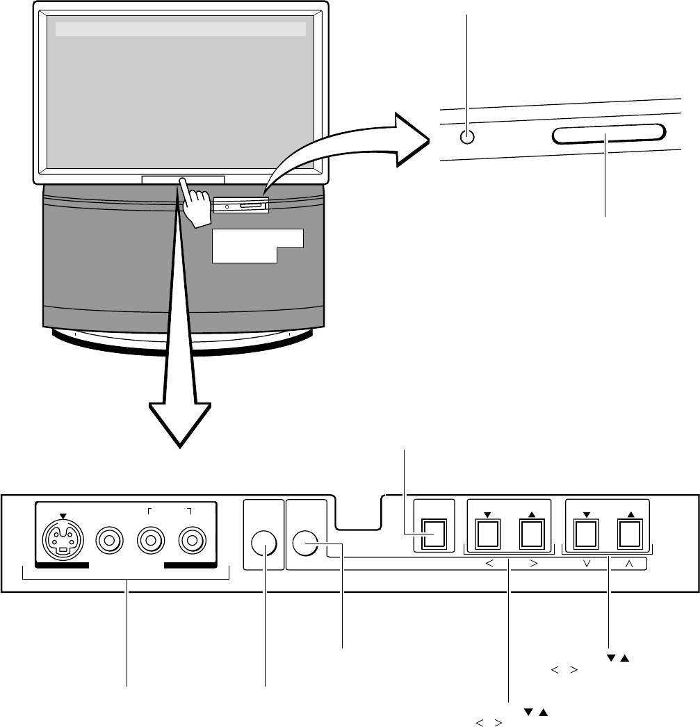
4. FRONT VIEW
Fig. 1-1
Note: [No] Owner's manual page.
POWER
DEMO
MENU
ANT/
VIDEO
ENTER
VOLUME CHANNEL
POWER indicator
POWER button
Press to open
the door.
Behind the door
ANT / VIDEO button **
ENTER button
S-VIDEO VIDEO
L/MCNO R
AUDIO
IN-VIDEO 3
VIDEO 3 INPUTS DEMO button
MENU button CHANNEL / buttons
/ buttons
VOLUME / buttons
/ buttons
8
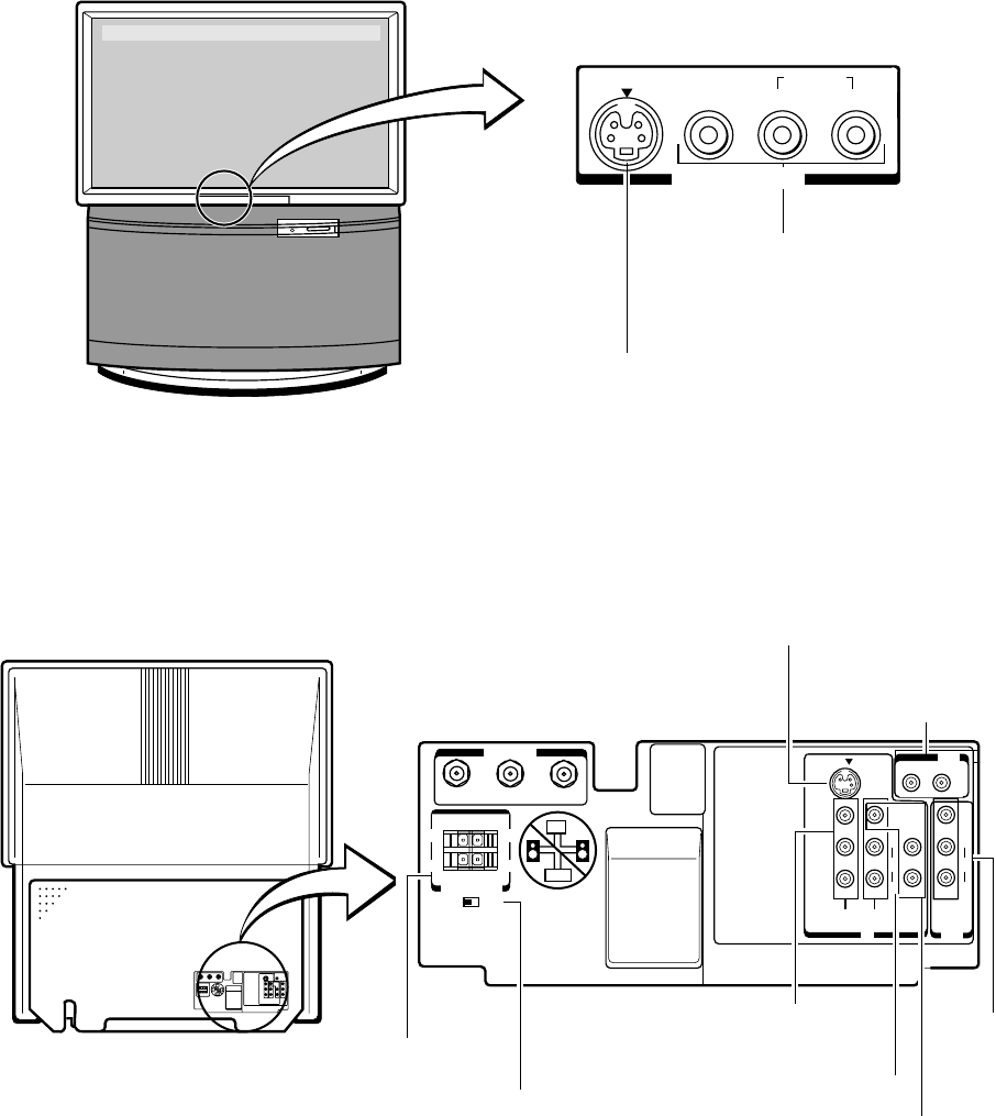
5. REAR VIEW
S-VIDEO VIDEO
L/MCNO R
AUDIO
IN-VIDEO 3
VIDEO / AUDIO INPUT jacks (VIDEO 3)
S-VIDEO INPUT jack (VIDEO 3)
Behind the door
TV front
Fig. 1-2
EXT SPEAKER
EXT INT
ANT (75 ½)
TV
AMP
L
VIDEO/AUDIO
R
VIDEO1
VIDEO
AUDIO
L
Y
S-VIDEO
C4
AUDIO
R
VIDEO
AMP
R
VIDEO
VIDEO2 DVD
L
RVAR
ACC
AMP
NCUT
MAIN SPEAKER
(+)
(Ð)
(+)
(Ð)
EXTERNAL
SPEAKER
terminal MAIN
SPEAKER
switch
VIDEO / AUDIO
INPUT jacks
(VIDEO 1)
VIDEO / AUDIO
INPUT jacks
(VIDEO 2) DVD INPUT
jacks
VIDEO /
AUDIO
OUTPU
T
jacks
S-VIDEO INPUT jack
(VIDEO 1)
VARIABLE AUDIO
OUTPUT jacks
TV rear
Fig. 1-3
9
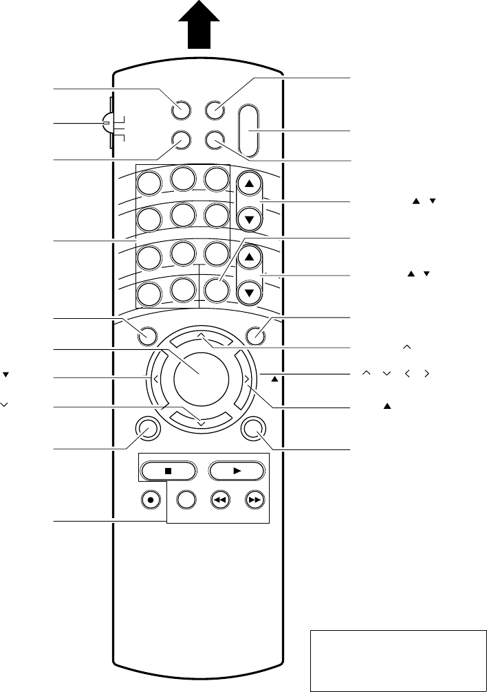
6. REMOTE CONTROL VIEW
ADV/
POP CH
ADV/
POP CH
23
56
89
4
7
¥
0
ENT
PIC -SIZE
TV/VIDEO
RECALL
POWER
CH
VOL
CH RTN
EDS MENU
FAV FAV
EXITRESET
STOP SCURCE PLAY POP
REC TV/VCR REW FF
CH SEARCH
STILL SWAP
MUTE
1
ENTER
TOSHIBA
RECALL* [ 26 ]
POWER [ 20 ]
MUTE* [ 26 ]
CHANNEL / [ 25 ]
CH RTN* [ 26 ]
VOLUME / [ 25 ]
MENU [ 18 ]
POP CH * [ 40 ]
///[ 18 ]
RESET * [ 33 ]
POP functions* [40]
(For " TV " and " CABLE " positions)
POP CH * [ 40 ]
FAN * [ 46 ]
ENTER [ 19 ]
EDS* [ 27 ]
Channel Number* [ 25 ]
TV / VIDEO* [ 55 ]
TV / CABLE / VCR switch [ 15 ]
Set to " TV " to control the TV.
TIMER* [ 38, 39 ]
EXIT * [ ON ]
Owner's Manual page
* These function do not have
duplicate locations on the TV.
They can be controlled only by
the Remote Control.
FAN * [ 46 ]
Aim at the remote sensor on the TV
100
TV
CABLE
VCR
Fig. 1-4
Note: [No] Owner's Manual page.
10
7. CHASSIS LAYOUT
-3 :
CRT-D(B)
5
-2 :
CRT-D(G)
5
-1 :
CRT-D(R)
5
- 6 : SVM
5FOCUS PACK
- 4 : FRONT-LED
5
- 5 : FRONT-CON
5
: POWER 1
6
F.B.T
J-BOX
To CRT
To FOCUS
PACK
330
294
: MAIN
1
1pc
330
294
: DEFELECTION
2
1pc
330
294
: CONV / POWER2
3
1pc
249
165
: AV.EXT SPK
4
1pcs
249
165
: POWER 1
6
1pc
330
249
:
CRT-1pcs
D/FRONT/SHV
5
4
-1: A.V
4
-2: SPEAKER
5
-1: CRTÐD ( R )
5
-2: CRTÐD ( G )
5
-3: CRTÐD ( B )
5
-4: FRONT LED
5
-5: FRONT CON
5
-6: SVH
7
-1: NEW OSD
7
-2: FRONT SURROUND
249
165
: NEW OSD/
FRONT SURROUND
7
2pcs
249
165
: SW DVD
8
4pcs
249
249
: POWER S.S
9
2pcs
242
160
: DIGITAL
CONVER
10
2pcs
CHIP DOUBLE FACED
TW56F80 ONLY
242
139
:DUAL
11
2pcs
CHIP DOUBLE FACED
242
155
:3D Y/C
12
2pcs
CHIP DOUBLE FACED
189
139
:MAC
13 4pcs
CHIP DOUBLE
FACED
330
139
:AUDIO LIVE
14
6pcs
CHIP SINGLE FACED
242
126
:SIARSIGHT
15
1pcs
CHIP DOUBLE FACED
242
113
:DOLBY PRO
16
2pcs
CHIP DOUBLE FACED
MODE1
TW40F80
TW56F80
TUNER DOLBY DSP F.SUR COHB FDS N.OSD STARSIGHT
2
2PRO 4CH
3DYC
3DYC
POWER STARSIGHT
(TW56F80 ONLY)
9
: DIGITAL
CONVER
10
: CONVERTER/POWER 2
3
REAR ANP
(TW56F80 ONLY)
CENTER AMP
(TW56F80 ONLY)
: SW DVD
8
- 3 : DPC
4
- 2 : SPEAKER
4- 1 : A/V
4
DOLBY
PRO
16
-2:
FRO.
SURR
7
YCS
12 - 6
: DUAL
11
: AUTOLIVE
14
:WAC
13
: MAIN
1
: DEFLECTION
2
: STARSIGHT
15
- 1: NEW OSD
7
TW56F80 ONLY
TW56F80 ONLY
(chip)
PC BOARD
Fig. 1-5
11
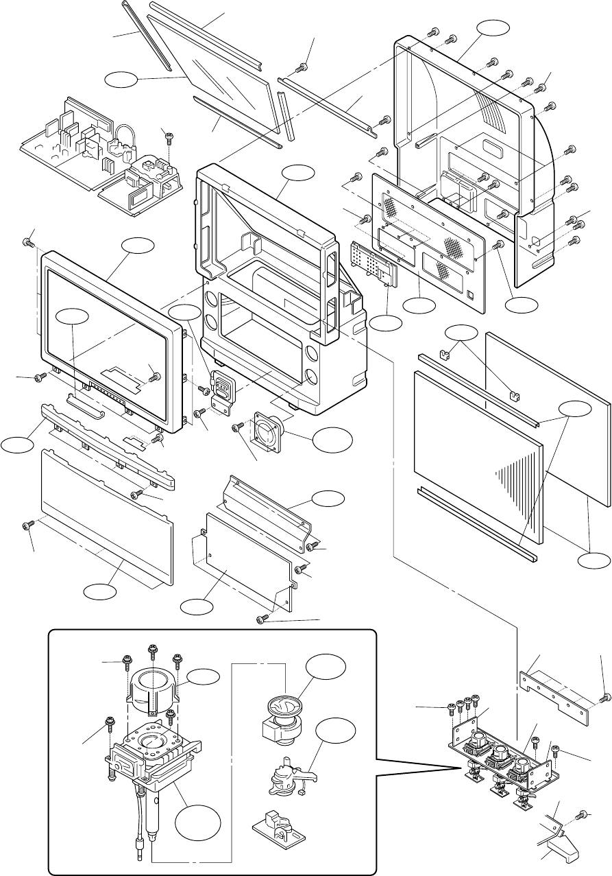
8. CONSTRUCTION OF CHASSIS
A110
A110B
2pcs
K601
A520
PP 5x18
4pcs
A110A
A126
A505
BIDT2
4x12 2pcs
A101
A401
A522
BIDT2
4X12 18pcs
A517
A353
A517
PBI 4X16
8pcs
B202
A351
A512
BIDT2
4x12 6pcs
A201
A902 Z410
A
502
PMM 4x16
4
pcs
A521
BRT TBS 4x16
2pcs
W661~
W664
PMM 4x16
2pcs
A506
BRB TBS
4x16 4pcs
A508
BIDT2
4x12 2pcs
A523
PMM 4x16
2pcs
A509
BTA 4x16 4pcs
A106
A102
A501
BTA 4x16 16pcs
A202
A516
PMS 3.8x28
3pcs
A515
PMM 4X16
4pcs
A205
A127
A128
K511
A519
BIDT2
4x12
5pcs
A107
A104
A105
A508
BIDT2
4x12
4pcs
A513
BIDT2
4x12
A104
A108
A105
A503
PMM
4x16
8pcs
L462~
L464
L472~
L474
K103
A511
PP4x14
4pcs
A510
BRBTB
5x16
4pcs
V901R
V902G
V903B
Fig. 1-6
12
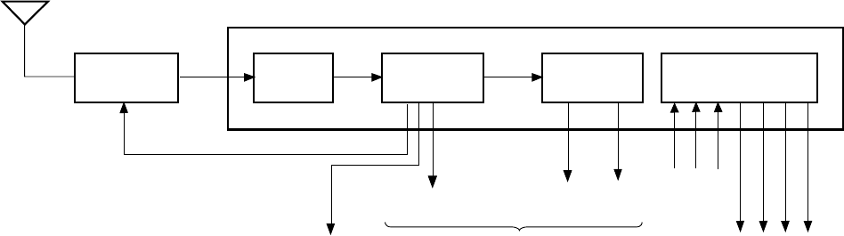
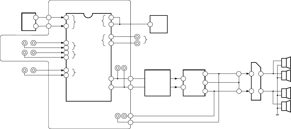
1. CIRCUIT BLOCK
Fig. 2-1 Block diagram
1-1. Outline
(1) RF signals sent from an antenna are converted into in-
termediate frequency band signals (video: 45.75 MHz,
audio: 41.25 MHz) in the tuner. (Hereafter, these sig-
nals are called IF signals.)
(2) The IF signals are band-limited in passing through a
SAW filter.
(3) The IF signals band-limited are detected in the VIF
circuit to develop video and AFT signals.
(4) The band-limited IF signals are detected in the SIF cir-
cuit and the detected output is demodulated by the au-
dio multiplexer, developing R and L channel outputs.
These outputs are fed to the A/V switch circuit.
(5) A sound processor (S.PRO.) is provided.
1-2. Major Features
(1) The VIF/SIF circuit is fabricated into a small module
by using chip parts considerably.
(2) As the tuner, EL466L that which contains an integrated
PLL circuit is employed.
(3) Wide band double SAW filter F1802R used.
(4) FS (frequency synthesizer) type channel selection sys-
tem employed.
EL466L
Tuner
RF AGC
IF/MTS/S.PRO Module MVUS34S
SIF
output
Sound
Multiplex
Circuit
SAW
Filter
VIF/SIF
Circuit S.PRO Circuit
AFT output
TP12
Video output
To A/V switch circuit
TV
R-OUT
TV
L-OUT
C-IN
R-IN L-IN
R-OUT L-OUT (L+R)
-OUT
C-OUT
(5) VIF/SIF circuit uses PLL sync detection system to
improve performances shown below:
• Telop buzz in video over modulation
• DP, DG characteristics (video high-fidelity repro-
duction)
• Cross color characteristic (coloring phenomenon
at color less high frequency signal objects)
(6) HIC SBX1637A-22 is used in the audio multiplexer
circuit to minimize the size with increased performance.
(7) As a sound control processor, TA1217N is used. I2C-
bus data control the DAC inside the IC to perform
switching of the audio multiplexer modes.
SECTION II: TUNER, IF/MTS/S. PRO MODULE
13
1-3. Audio Multiplex Demodulation Circuit
The sound multiplex composite signal FM-detected in the
PIF circuit enters pin 12 of HIC (hybrid IC) in passing
through the separation adjustment VR RV2 and amplified.
After the amplification, the signal is split into two: one en-
ters a de-emphasis circuit, and only the main signal with the
L-R signal and a SAP signal removed enters the matrix cir-
cuit. At the same time, the other passes through various fil-
ters and trap circuits, and the L-R signal is AM-demodu-
lated, and the SAP is FM-demodulated.
Then, both are fed to the matrix circuit. At the same time,
each of the stereo pilot signal fH and the SAP pilot signal
5fH is also demodulated to obtain an identification voltage.
With the identification voltage thus obtained and the user
control voltage are used to control the matrix.
The audio signals obtained by demodulating the sound mul-
tiplex signal develop at pin 10 and 11 of HIC and develop
the terminals of 12 and 14 of the module.
MVUS34S
MPX
Out DAC-out1
(SURR ON/OFF) DAC-out2
(RFSW)
TV
R-Out TV
L-Out
910 11 12 13 14 15
Stereo 0V SAP 0V OFF 0V
Other 5V Other 5V ON 9V
RF1 0V
RF2 9V
To AV select circuit
Monitor the input
pin for multiplex
sound IC
TV waveform detection
output (R) TV waveform detection
output (L)
Fig. 2-2 Block diagram of MVUS34S
Table 2-1 Matrix for broadcasting conditions and
reception mode
Broad- Switching Output OSD display
casted mode 12 pin 14 pin Stereo SAP
(R) (L)
Stereo STE R L •–
SAP R L •–
MONO L+R L+R •–
Mono STE L+R L+R – –
SAP L+R L+R – –
MONO L+R L+R – –
Stereo STE R L ••
+ SAP SAP SAP ••
SAP MONO L+R L+R ••
Mono STE L+R L+R – •
+ SAP SAP SAP – •
SAP MONO L+R L+R – •
Note:
Of the mode selection voltages, switching voltages for STE,
SAP, MONO do not output outside the module.
They are used inside the module to control the BUS.
• : Available, – : Not available
14
1-4. A.PRO Section (Audio Processor)
The S.PRO section has following functions.
(1) Woofer processing (L+R output)
(2) High band, low band, balance control
(3) Sound volume control, cyclone level control
(4) Cyclone ON/OFF
All these processing are carried out according to the BUS
signals sent from a microcomputer.
Fig. 2-3 shows a block diagram of the A.PRO IC.
TA1217N
Lin
Rin
Cin
Win
SDA
SCL
TONE CONTROL
LPF
Center
LEVEL
Woofer
LEVEL
VOLUME
BALANCE
I C
2
D/A
CONV
I/O
L out
R out
C out
W out
SAP Ident.
STE Ident.
R-in C-in L-in SCL SDA W-out O-out L-out
From From From
A/V Dolby A/V
to Q670 to Q640 to Q670 to Q670
Via QS101
731 24 23 22 19
26
25
18
10
30 9 828
127
29 22 32 36
456
17
16
15
14
13
12
11
34
30
2
3
20
21
Fig. 2-3 A.PRO block diagram
15
Fig. 2-4
Configuration of the audio circuit and signal flow are given
in Fig. 2-4
A/V PCB
ICV01
VIF+MTS+S.PRO
MODULE
R
L
R
L
L
R
L
R
L
R
L
R
L
R
MOTHER
TV
CHILD
TV
PIP
OUTPUT
VIDEO 1
VIDEO 2
VIDEO 3
FOR POP
IF MODULE
AUDIO
L
R
PIP OUT
(AUDIO)
VIDEO 1
VIDEO 2
OR
DVD
VIDEO 3
(FRONT INPUT)
R L
R L
R L
R
L
VIDEO
OUTPUT
TERMINAL
VARIABLE
AUDIO OUTPUT
TERMINAL
RL
FRONT
SURROUND
UNIT
VIF+MTS+A.PRO
MODULE
R
L
R
L
Q601 R
L
R OUT
L OUT
W OUT
12
14
EQ
ER
AS
AR
AI
AJ
6
7
11
13
3
9
15
17
29
31
2
1
35
37
16
18
25
24
22
2
5
11
7
+
+
(TW40F80 NOT USE)
16
2. POP TUNER
TUNER
SECTION
SAW
FILTER VIF/SIF
CIRCUIT
RF AGC
AFT
OUTPUT
VIDEO
OUTPUT
AUDIO
OUTPUT
Fig. 2-5
2-1. Outline
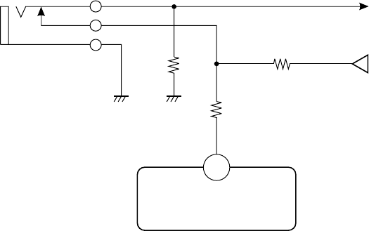
The POP tuner (EL922L) consists of a tuner and an IF block
integrated into one unit. The tuner receives RF signals in-
duced on an antenna and develops an AFT output, video
output, and audio output.
The tuner has receive channels of 181 as in the tuner for the
main screen and it is also controlled through the I2C-bus.
As the IC for the IF, a PLL complete sync detection plus
audio inter carrier system are employed.
Label
Name
Lot No.
115
Fig. 2-6 Tuner terminal layout
Terminal No. Name
1NC
2 32V
3 S-CLOCK
4 S-DATA
5NC
6 ADDRESS
75V
8 RF AGC
99V
10 AUDIO
11 GND
12 AFT
13 NC
14 GND
15 VIDEO
17
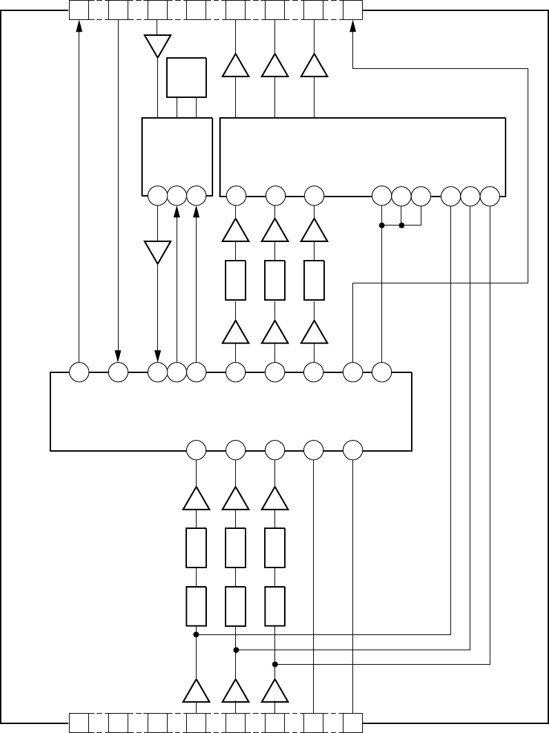
POP and Double Window signal processing (QY03), IC for
closed caption control (QM01), IC for WAC control (QX01),
IC for 3D-YCS (QZ01), IC for AUTOLIVE (QK06).
Differences from N5SS chassis are as follows;
1. On-screen function inside microcomputer is used. Sepa-
rate IC is not used for on-screen.
2. The microcomputer does not have the closed caption
function, but controls separate IC for closed caption.
3. The system uses two channels of I2C bus. One is only
for non-volatile memory.
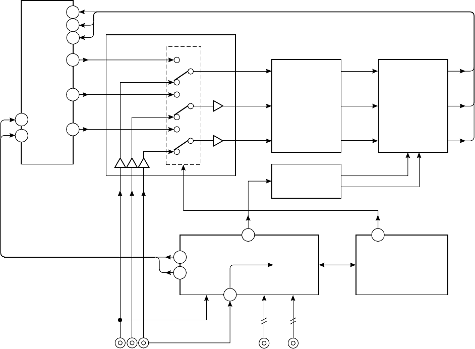
1. OUTLINE OF CHANNEL SELECTION CIRCUIT SYSTEM
The channel selection circuit in the N5SS chassis employs
a bus system which performs a central control by connect-
ing a channel selection microcomputer to a control IC in
each circuit block through control lines called a bus. In the
bus system which controls each IC, the I2C bus system (two
line bus system) developed by Philips Co. Ltd. in the Neth-
erlands has been employed.
The ICs controlled by the I2C bus system are: IC for V/C/D
signal processing (Q501), IC for A/V switching (QV01), IC for
non volatile memory (QA02), Main and sub U/V tuners (H001,
HY01), IC for deflection distortion correction (Q302), IC for
Toshiba made 8 bit microcomputer TLCS-870 series for TV
receiver, TMP87CS38N-3320 is employed for QA01.
With this microcomputer, each IC and circuit shown below
are controlled.
(1) CONTROL OF VIDEO/CHROMA/DEF SIGNAL
PROCESS IC (Q501 Toshiba TA1222AN)
• Adjustments for uni-color, brightness, tint, color
gain, sharpness and PIP uni-color
• Setting of adjustment memory values for sub-
brightness, sub-color and sub-tint, etc.
• Setting of memory values for video parameters such
as white balance (RGB cutoff, GB drive) and
gcorrection, etc.
• Setting of video parameters of video modes (Stan-
dard, Movie, Memory)
(2) CONTROL OF A/V SWITCH IC (QV01 Toshiba
TA1218N)
• Performs source switching for main screen and sub
screen
• Performs source switching for TV and three video
inputs
(3) CONTROL OF NON-VOLATILE MEMORY IC
(QA02 Microchip 24LC08BI/P)
• Memorizes data for video and audio signal adjust-
ment values, volume and woofer adjustment val-
ues, external input status, etc.
• Memorizes adjustment data for white balance (RGB
cutoff, GB drive), sub-brightness, sub color, sub
tint, etc.
• Memorizes deflection distortion correction value
data adjusted for each unit.
SECTION III: CHANNEL SELECTION CIRCUIT
2. OPERATION OF CHANNEL SELECTION CIRCUIT
(4) CONTROL OF U/V TUNER UNIT (H001 Toshiba
ELA12L, HY01 Toshiba EL922L)
• A desired channel can be tuned by transferring a
channel selection frequency data (divided ratio data)
to the I2C bus type frequency synthesizer equipped
in the tuner, and by setting a band switch data which
selects the UHF or VHF band.
(5) CONTROL OF DEFLECTION DISTORTION COR-
RECTION IC (Q302 Toshiba TA8859P)
• Sets adjustment memory value for vertical ampli-
tude, linearity, horizontal amplitude, parabola, cor-
ner, trapezoid distortion.
(6) CONTROL OF POP & Double Window SIGNAL PRO-
CESS IC (QY03 Toshiba TC9092AF, QY91 Sony
CXP85116B-514Q)
• Controls ON/OFF and 9 pictures serch of POP.
(7) CONTROL OF CLOSED CAPTION/EDS (QM01
Motorola XC144144P)
• Controls Closed Caption/EDS.
(8) CONTROL OF WAC (QX01 Toshiba TC9097F)
• Controls Wide Aspect.
(9) CONTROL OF 3D-YCS (QZ01 Toshiba TC9086F)
• Controls ON/OFF of 3 Dimension Y/C separator.
(10) CONTROL OF VERTICAL AMPLITUDE (QK06
Toshiba TMP87CM36N)
• Controls Wide Mode.
(11) CONTROL OF OSD (Do not I2C BUS) (QR60 Fujitsu
MB90091)
• Controls of OSD Menu.
18
Fig. 3-1
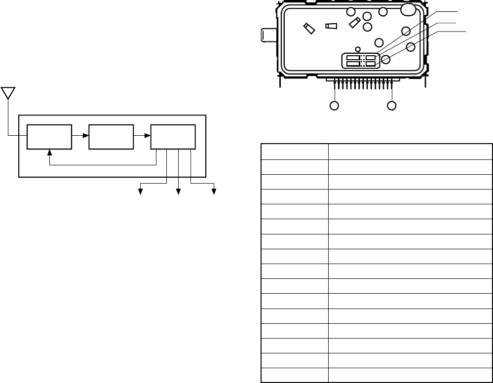
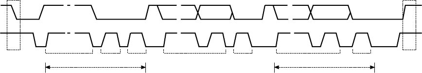
3. MICROCOMPUTER
Microcomputer TMP87CS38N-3320 has 60k byte of ROM
capacity and equipped with OSD function inside.
The specification is as follow.
• Type name : TMP87CS38N-3320
• ROM : 60k byte
• RAM : 2k byte
• Processing speed : 0.5m s (at 8MHz with Shortest com-
mand)
• Package : 42 pin shrink DIP
•I
2
C-BUS : two channels
• PWM : 14 bit x 1, 7 bit x 9
• ADC : 8 bit x 6 (Successive comparison system, Conver-
sion time 20ms)
IIC device controls through I2C bus. (Timing chart : See Fig.
3-1)
• LED uses big current port for output only.
• For clock oscillation, 8MHz ceramic oscillator is used.
•I
2
C has two channels. One is for EPROM only.
• Self diagnosis function which utilizes ACK function of
I2C is equipped
• Function indication is added to service mode.
• Remote control operation is equipped, and the control
by set no touch is possible. (Bus connector in the con-
ventional bus chassis is deleted.)
• Substantial self diagnosis function
(1) B/W composite video signal generating function
(micom inside, green crossbar added)
(2) Generating function of audio signal equivalent to
1kHz (micom inside)
(3) Detecting function of power protection circuit opera-
tion
(4) Detecting function of abnormality in IIC bus line
(5) Functions of LED blink indication and OSD indica-
tion
(6) Block diagnosis function which uses new VCD and
AV SW
SDA
SCL 1 - 7 891 - 7 891 - 7 89
Start
condition Stop
condition
Address R/W Ack Data Ack DATA Ack
Approx.180µSSome device may have no data,
or may have data with several
bytes continuing.
19
Fig. 3-2
4. MICROCOMPUTER TERMINAL FUNCTION
TMP87CS38N3320 (QA01)
I
O
O
O
O
O
O
O
I
O
IO
I
0
I
I
I
I
O
O
I
I
I
IO
O
I
I
I
I
O
I
I
O
I
I
0
O
I
O
O
GND
P40 (PWM0)
P41 (PWM1)
P42 (PWM2)
P43 (PWM3)
P44 (PWM4)
P45 (PWM5)
P46 (PWM6)
P47 (PWM7)
P50 (PWM8/TC2)
P51 (SCL1)
P52 (SDA1)
P53 (AINO/TC1)
P54 (AIN1)
P55 (AIN2)
P56 (AIN3)
P60 (AIN4)
P61 (AIN5)
P62
P63
VSS
VDD
P57
P32
P57
SDA0
SCL0
(TC3)P31
(RXIN)P30
P20
RESET
XOUT
XIN
TEST
0SC2
0SC1
VD
OSD RESET
DATA
BUSY
CS
CLK
1
2
3
4
5
6
7
8
9
10
11
12
13
14
15
16
17
18
19
20
21
GND
BAL
REM OUT
MUTE
SP MUTE
NC
POWER
LED
SSRST
DVD CONT
SCL0
SDA0
SYNC VCD
PIPRST
AFT2
AFT1
KEY-A
KEY-B
SGV
SGA
GND
IIC
-BUS
42
41
40
39
38
37
36
35
34
33
32
31
30
29
28
27
26
25
24
23
22
VDD
ACP
SS VD
I C STOP
SDA1
SCL1
SYNC AV1
RMT IN
EXT SP
RESET
XOUT
XIN
GND
0SC1
0SC2
VSYNC
OSD RESET
DATA
BUSY
CS
CLK
IIC-
BU
S
2

20
<< MICROCOMPUTER TERMINAL NAME AND OPERATION LOGIC >>
No. Terminal Name Function In/Out Logic Remarks
1 GND 0V
2 BAL INPUT BALANCE Out PWM out
3 REM OUT REMOTE CONTROL Out Remote control output
SIGNAL OUT
4 MUTE SOUND MUTE OUT Out Sound mute output
5 SP MUTE SPEAKER MUTE Out In muting = H
6 DEF POW Out
7 POWER POWER ON/OFF OUT Out Power control In ON = H
8 LED POWER LED OUTPUT Out Power LED on-control
LED lighting = L
9 SS RST STARSIGHT RESET Out Reset = L 0V
10 DVD CONT DVD CONTROL Out DVD = L, Other = H 0V
11 SCL0 IIC BUS CLOCK OUT Out IIC bus clock output 0
12 SDA0 IIC BUS DATA IN/OUT In/Out IIC bus data input/output 0
13 SYNC VCD H SYNC INPUT In Main picture H. sync signal input
14 PIP RST PIP RESET Out Reset = L
15 AFT2 IN In Sub tuner AFT S-curve input
16 AFT1 UV MAIN S-CURVE In Main tuner AFT S-curve
SIGNAL signal input
17 KEY A LOCAL KEY INPUT In Local key detection: 0 to 5V
18 KEY B LOCAL KEY INPUT In Local key detection: 0 to 5V
19 SGV TEST SIGNAL OUT Out Test signal output In normal = L 0V
20 SGA TEST AUDIO OUT Out Test audio output In normal = L 0V
21 VSS POWER GROUNDING — 0V: Gounding voltage 0V
22 CLK CLOCK OSD Out At display on: Pulse
23 CS CHIP SELECT Out At display on: Pulse
24 BUSY BUSY OSD In At display on: Pulse
25 DATA DATA OSD Out At display on: Pulse
26 OSD RESET RESET OSD Out Reset = L
27 VSYNC In VSYNC Pulse
28 OSC1 DISPLAY CLOCK Out 4.5MHz Pulse
29 OSC2 DISPLAY CLOCK In Pulse
30 TEST TEST MODE In GND fixed 0V
31 XIN SYSTEM CLOCK In System clock input 8MHz pulse
32 XOUT SYSTEM CLOCK Out System clock output 8MHz 8MHz pulse
33 RESET SYSTEM RESET In System reset input (In reset = L) 5V
34 EXT SP EXTERNAL SPEAKER In EXTERNAL = L, INT = H
35 RMT IN REMOTE CONTROL In In remote control pulse input = L In reception of
SIGNAL INPUT remote pulse
36 SYNC AV1 HSYNC INPUT In External H. sync signal input Pulse
37 SCL1 IIC BUS CLOCK OUT Out IIC bus clock output 1 Pulse
38 SDA1 IIC BUS DATA IN/OUT In/Out IIC bus data input/output 1 Pulse
39 I2C STP IIC BUS STOP In STOP = L
40 SS VD STARSIGHT VD In VSYNC for Starsight Pulse
41 ACP NSYNC INPUT In AC pulse input
42 VDD POWER — 5V 5V
21
5. EEPROM (QA02)
EEPROM (Non volatile memory) has function which, in spite
of power-off, memorizes the such condition as channel se-
lecting data, last memory status, user control and digital pro-
cessor data. The capacity of EEPROM is 8k bits.
Fig. 3-3
A0
A1
A2
Vss
Vcc + 5V
NC
SCL
SDA
I
2
C-BUS line
Device adress
GND
EEPROM(QA02)
1
2
3
4
8
7
6
5
Fig. 3-4
6. ON SCREEN FUNCTION
The OSD system of TW40F80 employs the external OSD
IC (QR60, MB90091) to obtain high quality OSD.
54
56
58
55
16
64
59
60
61
22
23
24
25
26
R OUT
G OUT
B OUT
SCLK
SCS
TRE
SIN
RESET
VOB2
VIDEO
(YM)
CLK
CS
BUSY
DATA
OSD RESET
QR60 MB90091QA01 Microprocessor
QR60 is controlled by the microprocessor QA01 with the
exclusive control signals of CLK, DATA, CS, BUSY, RE-
SET.
Type name is 24LC08BI/P or ST24C08CB6, and those are
the same in pin allocation and function, and are exchange-
able each other. This IC controls through I2C bus. The power
supply of EEPROM and MICOM is common. Pin function
of EEPROM is shown in Fig. 3-3.
22
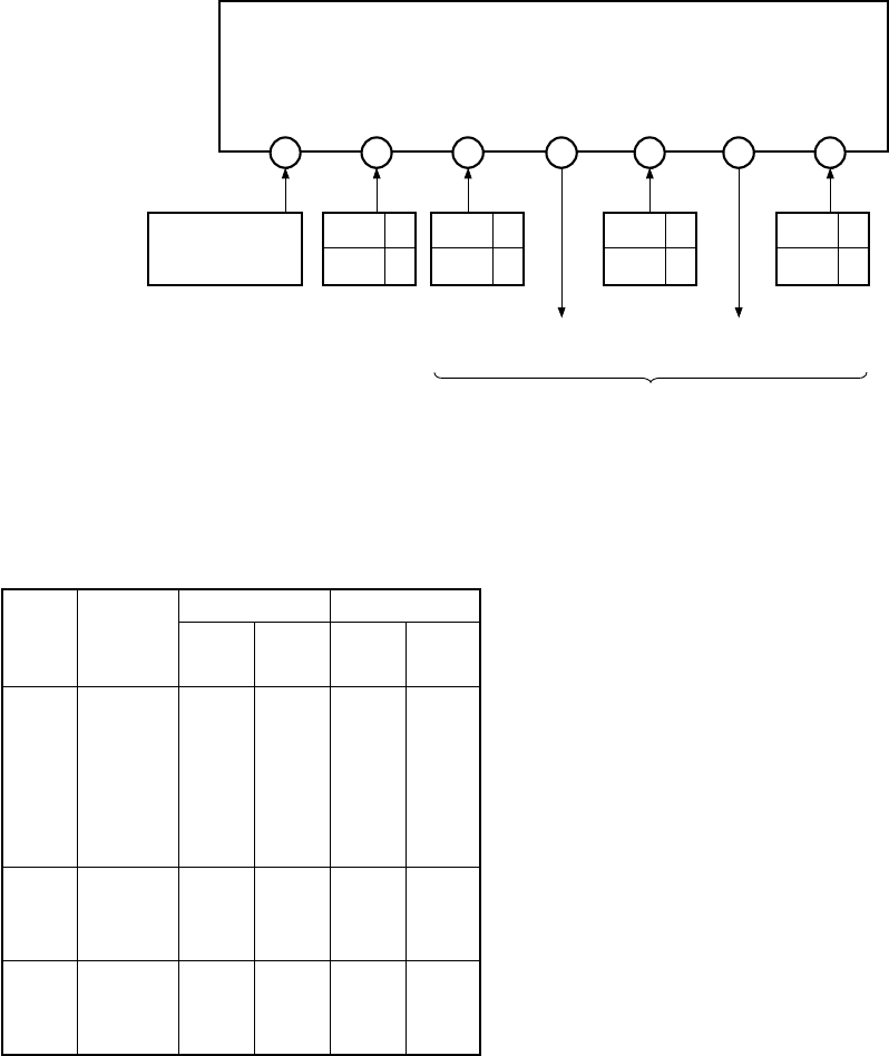
7. SYSTEM BLOCK DIAGRAM
SCL 0
11
SDA 0
12
VSYNC
27
INT4
40
RMT OUT
3
MUTE
4
SP MUTE
5
V.sync
pulse
Audio mute
Speaker
mute
Remote
controller
output
6
5
QA02
Memory
24LC08BI/P
SDA SCL
DATA
25
CLK
22
CS
23
BUSY
24
RESET
26
15
14
QH30
C/C,EDS
XC144144P
SDA SCL
5856
CS BUSY
55
DATA
54
CLK
QR60
OSD
MB90091
59
60
QX01
WAC
TC9097F
SDA SCL
43
44
Q701
CONVER
T7K64
SDA SCL
HO01
SDA SCL
Main U/V tuner
ELA12L
HY01
SDA SCL
Sub U/V tuner
EL922L
2827
Q501
SDA SCL
VCD
TA1222AN
2021
HO02
SDA SCL
IF/MPX/A.PRO
MVUS5345
25
24
QV01
SDA SCL
AV SW
TA1218N
DPC unit
1920
QZ01
SDA SCL
YCS
TC9086F
QY91
SDA SCL
DUAL micro-
processor
39
40
QK06
SDA SCL
AUTO LIVE
38
SDA 1
37
SCL 1
35
RMT Remote
controller
light
receiving
unit
17
KEY-A Key
switch
33
RST
42
VDD
1
GND
21
VSS
7
POWER
31
XIN
8
LED
41
ACP
Power
supply
circuit
32
XOUT 8MHz
Clock
19
SGV
20
SGA
Signal
output
36
SYNC-AV1
16
AFT1 IN
Main screen
Sync det.
AFT det.
13
SYNC-AV2
2
AFT2 IN
Sub screen
Sync det.
AFT det.
18
KEY-B
QY03
POP
TC9092F
DATA CLK
QA01
TMP87CS38N-XXXX
Fig. 3-5
23
8. LOCAL KEY DETECTION METHOD
Local key detection in the N5SS chassis is carried out by
using analog like method which detects a voltage appears at
local key input terminals (pins 17 and 18) of the microcom-
puter when a key is pushed. With this method using two
local key input terminals (pins 17 and 18), key detection up
to maximum 14 keys will be carried out.
The circuit diagram shown left is the local key circuit. As
can be seen from the diagram, when one of keys among SA-
01 to SA-08 is pressed, each of two input terminals (pins 17
and 18) developes a voltage VIN corresponding to the key
pressed. (The voltage measurement and key identification
are carried out by an A/D converter inside the microproces-
sor and the software.
17 18
SA08
SA06
SA05
SA07
SA01
SA02
SA03
SA04
Fig. 3-6 Local key assignment
Table 3-1 Local key assignment
Key No. Function Key No. Function
SA-02 POWER SA-01
DEMO START/STOP
SA-03 CH UP
SA-04 CH DN
SA-05 VOL UP
SA-06 VOL DN
SA-07 ANT/VIDEO, ADV
SA-08 MENU
24
9. REMOTE CONTROL CODE ASSIGNMENT
Custom codes are 40-BFH (TV set for North U.S.A.)
Code Applicable Applicable Conti-
Function to remote to TV set nuity
control
50H PIP STILL
51H PIP ON/OFF
52H Do not use. Old type core power ON
53H PIP SWAP
54H PIC SIZE
55H DSP F/R
56H WIDE/SCROLL
57H CAPTION
58H EXIT
59H CYCLONE, SBS
5AH SET UP
5BH OPTION
5CH SUB WOOFER UP
5DH
SUB WOOFER DOWN
5EH
5FH
80H MENU
81H EDS
82H ADV UP
83H ADV DWN
84H
85H GUIDE
86H THEME
87H LIST
88H PIP CONTROL
89H ENTER/TUNE
8AH PAGE UP
8BH DATA UP
8CH PAGE DN
8DH DATA DN
8EH CANCEL
8FH REC
90H
91H
92H Do not use. Old type core power ON
93H
94H
95H
96H
97H NOISE CLEAN
98H
99H
9AH PIP VOLUME UP
9BH
9CH PIP CONTROL
9DH
9EH PIP VOLUME DOWN
9FH
Custom codes are 40-BFH (TV set for North U.S.A.)
Code Applicable Applicable Conti-
Function to remote to TV set nuity
control
00H 0 Channel
01H 1 Channel
02H 2 Channel
03H 3 Channel
04H 4 Channel
05H 5 Channel
06H 6 Channel
07H 6 Channel
08H 8 Channel
09H 8 Channel
0AH 100 Channel
0BH ANT 1/2
0CH RESET
0DH AUDIO
0EH PICTURE/FUNC
0FH TV/VIDEO
10H MUTE
11H CHANNEL SEARCH
12H POWER
13H MTS
14H ADD/ERASE
15H TIMER/CLOCK
16H AUTO PROGRAM
17H CHANNEL RETURN
18H DSP/SUR (TV/CATV)
19H CONTROL UP
1AH VOLUME UP
1BH CHANNEL UP
1CH RECALL
1DH CONTROL DOWN
1EH VOLUME DOWN
1FH CHANNEL DOWN
40H PIP LOCATE
41H PIP LOCATE
42H PIP LOCATE
43H PIP LOCATE
44H CARVER
45H SURROUND UP
46H SURROUND DOWN
47H VOCAL ZOOM
48H CHANNEL LOCK
49H
4AH PIP CHANNEL UP
4BH PIP CHANNEL DOWN
4CH PIP STILL/RELEASE
4DH
PIP ZOOM, ZOOM SIZE
4EH PIP LOCATE (CH SEARCH)
4FH PIP SOURCE
25
Custom codes are 40-BFH (TV set for North U.S.A.)
Code Applicable Conti-
Function to TV set nuty
D0H
D1H
D2H Do not use. Old type core power ON
D3H
D4H
D5H
D6H
D7H PIP VIDEO ADJ.
D8H STILL, FRAME ADVANCE
D9H
DAH SPEED
DBH
DCH ZOOM
DDH
DEH
DFH
E0H
PINCUTION/EW CORER (PARA/CNR)
E1H
VERTICAL S-CUVE CORRECTION/
VERTICAL M-CURVE
CORRECTION (VSC/FVC)
E2H
E3H
E4H
E5H
E6H
E7H
E8H
E9H
EAH
HORIZONTAL WIDTH (WID/PARA)
EBH
TRAPEZOIDE CORRECTION (TRAP)
ECH TEST TONE
EDH DOLBY
EEH
3 DIMENTIONAL Y/C SEPARATION
EFH DPC
E0H
STANDARD (HEIGHT LINEARITY) (VLIN/HIT)
E1H
WIDE (HEIGHT ® LINEARITY) (VLIN)
F2H SCROOL
F3H
WIDE 1, 2, 3
F4H
F5H
F6H
F7H
F8H
F9H
FAH
FBH
FCH
FDH
FEH
FFH
Custom codes are 40-BFH (TV set for North U.S.A.)
Code Applicable Conti-
Function to TV set nuty
A0H SUB-BRIGHT ADJUSTMENT
A1H G. DRIVE ADJUSTMENT
A2H B. DRIVE ADJUSTMENT
A3H
A4H
CUTOFF DRIVE 40H INITIALIZING,
HORIZONTAL ONE LINE
A5H R. CUTOFF ADJUSTMENT
A6H G. CUTOFF ADJUSTMENT
A7H B. CUTOFF ADJUSTMENT
A8H
MEMORY ALL AREA INITIALIZE
A9H PIP BRIGHT ADJUSTMENT
AAH SUB CONTRAST ADJUSTMENT
ABH
HOR, VER PICTURE POSITON ADJUSTMENT
ACH SUB COLOR ADJUSTMENT
ADH SUB TINT ADJUSTMNET
AEH ADJUSTMENT-UP
AFH ADJUSTMENT-DOWN
B0H
HORIZONTAL ONE LINE: SERVICE
B1H DSP ON/OFF
B2H TEXT-1
B3H
TV/PIP VIDEO CHANGE-OVER
B4H CAPTION-1
B5H
B6H
B7H TV/CABLE CHANGE-OVER IN
SAME TIME ON MAN AND SUB
B8H HOTEL SETTING MENU
B9H DATA 4 TIMES SPEED UP
BAH DATA 4 TIMES SPEED DOWN
BBH
CHANGE-OVER OF HOTEL/NORMAL
BCH PIP CENTER
BDH M MODE
BEH CAPTON OFF
BFH ALL CHANNEL PRESET
C0H
C1H DIRECT WIDE 1
C2H DIRECT FULL
C3H
C4H
C5H
C6H
C7H
C8H
C9H
CAH
CBH
CCH
CDH
CEH
CFH
26
MODELS
CN35F90
CN35F95
CX35F70
TW56F80
TW40F80
TP61F90
TP61F80
TP55F80
TP55F81
TP50F90
TP50F60
TP50F61
D7
0
0
1
0
1
0
0
0
0
0
1
1
D6
*
*
*
*
*
*
*
*
*
*
*
*
D5
0
0
0
0
0
0
0
0
0
0
0
0
D4
0
0
1
0
1
0
1
1
1
0
1
1
D2
0
0
0
0
0
0
0
0
0
0
0
0
D1
0
0
1
1
1
1
1
1
1
1
1
1
D3
*
*
*
*
*
*
*
*
*
*
*
*
D0
*
*
*
*
*
*
*
*
*
*
*
*
HEX
00H
00H
02H
02H
92H
02H
12H
12H
12H
02H
92H
92H
D7
0
0
0
0
0
0
0
0
0
0
0
0
D6
0
0
0
0
0
0
0
0
0
0
0
0
D5
0
0
0
0
0
0
0
0
0
0
0
0
D4
0
0
0
1
1
1
1
1
1
1
1
1
D2
0
0
0
1
0
1
0
0
0
1
0
0
D3
0
0
0
1
1
1
0
0
0
0
0
0
D0
*
*
*
*
*
*
*
*
*
*
*
*
HEX
00H
00H
00H
1CH
18H
1CH
18H
10H
10H
14H
10H
10H
D1
*
*
*
*
*
*
*
*
*
*
*
*
OPT0 OPT1
Normal 0/Free run 1
NON0/CONV1
NON0/3DYC
NON0/DOLBY1
NOT USED
NOT USED
DSP0/SRD1
NOT USED
PP0/MP1
SS/0 NONSS/1
NOT USED
Normal 0/f0 STOP 1
CYC0/SBS1
NOT USED
MODE:
Fixed
Normal00
STD: 01
HRC: 10
1RC: 11
9-1. Optional Setting for Each Model
• When the character generation is changed from
MB90091-107 TO MB90091-108, D5 bit of OPT0 in
the design data should be set to “1”.

27
10. ENTERING TO SERVICE MODE
1. PROCEDURE
(1) Press once MUTE key of remote hand unit to indicate
MUTE on screen.
(2) Press again MUTE key of remote hand unit to keep
pressing until the next procedure.
(3) In the status of above (2), wait for disappearing of in-
dication on screen.
(4) In the status of above (3), press MENU (Channel set-
ting) key on TV set.
2. Service mode is not memorized as the last-memory.
3. During service mode, indication S is displayed at upper
right corner on screen.
11. TEST SIGNAL SELECTION
1. In OFF state of test signal, SGA terminal (Pin 20) and
SGV terminal (Pin 21) are kept “L” condition.
2. The function of VIDEO test signal selection is cyclically
changed with VIDEO key (remote unit).
12. SERVICE ADJUSTMENT
1. ADJUSTMENT MENU INDICATION ON/OFF :
MENU key (on TV set)
2. During display of adjustment menu, the followings are
effective.
a) Selection of adjustment item :
POS UP/DN key (on TV/remote unit)
b) Adjustment of each item :
VOL UP/ DN key (on TV / remote unit)
c) Direct selection of adjustment item
R CUTOFF : 1 POS (remote unit)
G CUTOFF : 2 POS (remote unit)
B CUTOFF : 3 POS (remote unit)
d) Data setting for PC unit adjustment
SUB CONTRAST : 4 POS (remote unit)
SUB COLOR : 5 POS (remote unit)
SUB TINT : 6 POS (remote unit)
e) Horizontal line ON/OFF : VIDEO (on TV set)
f) Test signal selection : VIDEO (remote unit)
* In service mode, serviceable items are limited.
3. Test audio signal ON / OFF : 8 POS (remote unit)
* Test audio signal : 1 kHz
4. Self check display : 9 POS (remote unit)
* Cyclic display (including ON/OFF)
5. Initialization of memory :
CALL (remote unit) + POS UP (on TV set)
6. Initialization of self check data :
CALL (remote unit) + POS DN (on TV set)
7. BUS OFF :
CALL (remote unit) + VOL UP (on TV set)
Test Signal No.
0
1
2
3
4
5
6
7
8
9
10
11
12
13
14
15
Name of Pattern
Signal OFF
All black signal + R single color (OSD)
All black signal + G single color (OSD)
All black signal + B single color (OSD)
All black signal
All white signal
W/B
Black cross bar
White cross bar
Black cross hatch
White cross hatch
White cross dot
Black cross dot
H signal (bright area)
H signal (dark area)
Black cross + G signal color
(3) SGA (audio test signal) output should be square wave
of 1 kHz.
Table 3-2
28
13. FAILURE DIAGNOSIS PROCEDURE
Model of N5SS chassis is equipped with self diagnosis func-
tion inside for trouble shooting.
13-1. Contents to be Confirmed by Customer
Contents of self diagnosis
Contents of self diagnosis
< Countermeasure in case that phonomenon always arises >
B. Detection of shortage in BUS line.
C. Check of comunication status in BUS line.
D. Check of signal line by sync signal detection.
E. Indication of part code of microcomputer (QA01).
F. Number of operation of power protection circuit.
Display items and actual operation
Display items and actual operation
(Example of screen display)
SELF CHECK
Part coce of QA01
Number of operation of
power protection circuit
Short check of bus line
Communication check of
busline
NO. 239XXXX
POWER: 000000
BUS LINE: OK
BUS CONT: OK
BLOCK: UV V1 V2
QV01, QV01S
E
F
B
C
D
Table 3-3
Contents of self diagnosis
A. DISPLAY OF FAILURE INFORMATION IN NO
PICTURE (Condition of display)
1. When power protection circuit operates;
2. When I2C-BUS line is shorted;
Display items and actual operation
Power indicator lamp blinks and picture does not come.
1. Power indicator red lamp blinks. (0.5 seconds interval)
2. Power indicator red lamp blinks. (1 seconds interval)
If these indication appears, repairing work is required.
13-2. Contents to be Confirmed in Service Work (Check in self diagnosis mode)
Table 3-4
13-3. Executing Self Diagnosis Function
[CAUTION]
(1) When executing block diagnosis, get the desired input
mode (U/V BS VIDEO1, 2, 3) screen, and then enter
the self diagnosis mode.
(2) When diagnos other input mode, do again diagnosis
operation.
13-3-1. Procedure
(1) Set to service mode.
(2) Pressing “9” key on remote unit displays self diagno-
sis result on screen.
Every pressing changes mode as below.
(3) To exit from service mode, turn power off.
SERVICE mode SELF DIAGNOSIS mode
29
13-4. Understanding Self Diagnosis Indication
In case that phenomenon always arises. See Fig. 3-7 .
(Example of screen display)
SELF CHECK
Part coce of QA01
Number of operation of
power protection circuit
Short check of bus line
Communication check of
busline
NO. 239XXXX
POWER: 000000
BUS LINE: OK
BUS CONT: OK
BLOCK: UV V1 V2
QV01, QV01S
E
F
B
C
D
Table 3-5
Item
BUS LINE
BUS CONT
BLOCK: UV1
UV2
V1
V2
Contents
Detection of bus line short
Communication state of bus line
The sync signal part in each video signal
supplied from each block is detected.
Then by checking the existence or non of sync
part, the result of self diagnosis is displayed
on screen. Besides, when “9” key on remote
unit is pressed, diagnosis operation is first
executed once.
Instruction of results
Indication of OK for normal result, NG for abnormal
Indication of OK for normal result
Indication of failure place in abnormality
(Failure place to be indicated)
QA02 NG, H001 NG, Q501 NG, H002 NG, QV01 NG, Q302
NG, QY02 NG, HY01 NG, QD04 NG, QM01 NG, Q701 NG
Note:
The indication of failure place is only one place though
failure places are plural. When repair of a failure place
finishes, the next failure place is indicated. (The order of
priority of indication is left side.)
*Indication by color
• Normal block : Green
• Non diagnosis block : Cyan
Fig. 3-7

30
13-4-1. Clearing method of self diagnosis result
In the error count state of screen, press “CHANNEL DOWN”
button on TV set pressing “DISPLAY” button on remote unit.
CAUTION:
All ways keep the following caution, in the state of service
mode screen.
• Do not press “CHANNEL UP” button. This will cause
initialization of memory IC. (Replacement of memory
IC is required.)
• Do not initialize self diagnosis result. This will change
user adjusting contents to factory setting value. (Adjust-
ment is required.)
13-4-2. Method utilizing inner signal
(VIDEO INPUT 1 terminal should be open.)
(1) With service mode screen, press VIDEO button on re-
mote unit. If inner video signal can be received, QV01
and after are normal.
(2) With service mode screen, press “8” button on remote
unit. If sound of 1 kHz can be heard, QV01 and after
are normal.
* By utilizing signal of VIDEO input terminal, each circuit
can be checked. (Composite video signal, audio signal)
White
Yellow Cyan Green Magenta Red Blue
(COLOR BAR SIGNAL)
Color elements are positioned in sequence of
high brightness.
31
14. TROUBLESHOOTING CHART
14-1. TV does Not Turned ON
TV does not turned on.
Relay sound
Check of voltage at pin 7 of QA01
(DC 5V).
8MHz oscillation waveform
at pin 32 of QA01.
Pulse output at pins 37 and 38 of QA01.
Check relay driving circuit.
Check power circuit.
Check OSC circuit.
Replace QA01.
Voltage check at pin 32 of QA01
(DC 5V)
Check reset circuit.
Replace QA01.
YES
NG
NG
NG
NG
OK
NO
OK
OK
OK
32
14-2. No Acception of KEY-IN
14-3. No Picture (Snow Noise)
NG
OK
No picture
Voltage at pins of +5V, and 32V.
Check H001. Check tuner power circuit.
Key on TV
Voltage change at pins 17, 18 of
QA01 (5V to 0V).
Replace QA01.
Check key-in circuit.
NG
OK
NG
OK
Remote unit key
Pulse input at pin 35 of QA01,
When remote unit key is pressed.
Replace QA01
Check tuner power circuit.
33
14-5. No Indication On Screen
14-4. Memory Circuit Check
NG
NG
OK
OK
OK
No indication on screen.
Check of RESET at 5V.
Check of CLK, CS, BUSY, DATA at
pin 22, 23, 24, 25 of QA01.
"H" = 5V or puls?
Check of character signal at pin 59, 60, 61
of QR60 (5V(p-p)).
Check V/C/D circuit.
Replace QA01 or QR60 or QR63.
Replace QA01 or QR60.
Replace QR60.
NG
NG
NG
OK
OK
Memory circuit check
Voltage check at pin 8 of QA02 (5V).
Pulse input at pins 5 and 6 of QA02
in memorizing operation.
Replace QA02.
Adjust items of TV set adjustment.
Note: Use replacement parts for QA02.
Check power circuit.
Check QA01.
34
1. DVD SWITCH BLOCK DIAGRAM
53
52
51
4
5
6
13
15
C
Y
Y
Q
I
Y
Q
I
DVD SWITCH UNIT
QW01 TC4053BP
L
H
L
H
L
H
WAC UNIT
Y
Q (B - Y)
I (R- Y)
Y
Q
I
Y
Q
IYC
DUAL UNIT
Sub V.
Sub Y.
Sub C.
ZY01 Y/C SEPARATOR
42
Sub V.
36
34
Y
C
QV01 AV SW
TA1218N
21
VIDEO
3VIDEO
1
Insertion detection
10
DVD CONTROL
I C BUS
2
QA01
MAICROPROCESSOR
"L" = Normal
"H" = DVD
VIDEO2/
DVD
Q501 VCD
TA1222AN
I C BUS
2
MAIN
Y, Cr, Cb
Fig. 4-1
SECTION IV: DVD SWITCH CIRCUIT
35
2. OUTLINE
In this model, the DVD input terminals are provided in or-
der to receive the color difference signals (Y, Cr, Cb) out-
put from a DVD player.
The luminance (Y) signal input for DVD input uses the
VIDEO input terminal in common with the VIDEO 2 input.
The terminals for color difference signal inputs Cr (R – Y)
and Cb (B – Y) are used exclusively.
The input identification for VIDEO 2 and DVD is carried
out by setting pin 21 of QV01 TA1218N (AV SW IC) from
“L” to “H” when the cable is connected to the Cb input ter-
minal with a switch equipped.
The main microprocessor QA01 sets pin 10 of QA01 from
“L” to “H” through I2C bus when pin 21 of AW SW IC
develops “H”.
Cb input
Open : at Cb input
RV26
75
RV27
10k
RV28 100k
+9v
Cb to DVD SW uni
t
21
QV01 TA1218N
Fig. 4-2
36
1. OUTLINE
A wide aspect conversion (hereafter called WAC) process (3/4
compression process in 4:3 mode and 1/2 compression process
on left screen in double window mode) is performed inside the
WAC unit (PB6348) in TW40F80.
Screen modes for TF40F80 contain THEATER WIDE1, THE-
ATER WIDE 2, THEATER WIDE3, FULL, NORMAL and
DOUBLE WINDOW modes. The video signal compression is
carried out only when either the NORMAL or DOUBLE WIN-
DOW mode is selected. In the modes other than the NORMAL
and DOUBLE WINDOW mode, the video signal input to WAC
unit is output without performing any process.
The screen in the DOUBLE WINDOW mode creates a single
screen by superimposing the left screen processed in the WAC
unit on the right screen processed in the DUAL unit.
On the left screen, the video signal sent is time-compressed to 1/
2 in horizontal direction to fit in the left half of the wide screen
with 16:9 aspect ratio. In this case, a black level of DC is at-
tached on the right half of the screen in this circuit. However,
this is superimposed on the right screen, so nothing is visible on
the screen.
In the normal screen, the video signal is 3/4 time-compressed
and side panels in the black level are added on sides of the screen.
2. CIRCUIT OPERATION
2-1. Configuration
The WAC unit consists of a wide aspect conversion IC (QX01,
TC9097F, working as a central device), clock generation IC
(QX02, TA8667F), switch IC (QX03, TC4053BF), and periph-
eral circuits (LPF, AMP, emitter follower, etc.). The QX01
(TC9097F) contains an A/D converter, D/A converter, clamp cir-
cuit, VCO circuit, etc. and performs compression process, etc.
inside the IC for analog video signals entered according to con-
trols through IIC bus, thus providing the signal as an analog sig-
nal.
2-2. Operation
2-2-1. Signal Flow
Fig. 5-1 shows a block diagram of this circuit. A Y signal en-
tered through pin 6 of PX01 passes a low pass filter an a 6 dB
amplifier, and enters pin 3 of QX01. On the other hand, I and Q
signals enter through pin 4 and 5 of PX01,
and pass a low pass filter and amplifiers in the same way as the
Y signal, and enter pins 1 and 78 of QX01 respectively.
The Y , I and Q signals entered are clamped by built-in clamp
circuit, converted into digital signals by the built-in A/D con-
verter. Moreover, their read/write operations are rated up by twice
or 3/4 times to perform a compression process of 1/2 or 3/4
times inside the built-in line memory. And then, a black level
signal is added to the open area (right half, or both sides of
screen). Next, the signal is converted to an analog Y, I, and Q
signals by a built-in D/A converter and output from pins 17, 13,
and 9. Parameters of 1/2, 3/4 phase of the video signal, phase of
the side panel, etc. are controlled through I2C bus, control sig-
nals of which enters from pins 7 and 8 of PX01.
Thus processed signals are fed to a low pass filter to remove
high frequency noises generated in QX01 and then fed to the
QX03 switching IC. The compressed signal and a not compressed
signal entered from PX01 are directly fed to QX03, and switched
by a signal showing compression/not compression (NCS = out-
put from pin 61 of QX01 and fed to the receive unit through
pins 5, 6, and 7 of PX02.
2-2-2. Clock Generation
The system clock for QX01 is generated by QX02 according to
an H reference signal supplied from pin 3 of PX02 and fed to
QX01 through QX19 and QX40. (The frequency is adjusted to
28.7 ± 0.2 MHz with LX18).
The compressing operation is carried out by setting the write
clock to 1/2 or 3/4 times by the built-in VCO with the reading
clock fed to pin 47 of QX01.
2-2-3. Timing Pulse Generation
Moreover, the WAC unit generates following timing pulses.
(1) VPout
Reference signal entered through pin 2 of PX02 enters pin
3 of QX01, and outputs at pin 8 of PX02 after delayed by
an amount required. The vertical reference signal is out-
put in modes other than the normal and double window
and fed to the vertical circuit. Accordingly, the raster be-
comes an horizontal one when the unit is disconnected.
(2) HVBLK
This pulse is a timing pulse showing a black extension
mask period in the normal and double window modes. It
outputs at pin 1 of PX02 and enters pin 30 of Q501 in the
receive unit.
SECTION V: WAC CIRCUIT
37
LPF
AMP
QX28 QX29 LX14 etc
QX26 QX27 LX13 etc
QX10
QX15
ISI
QSI Y WA
I WA
Q WA
I TH
Q TH
Y TH
YSI
IBC QSO
ISO
YSO
HRE
VMO
RCK
VDI
VBL
IBD
QX13
QX11
QX06 LX12 etc
1
151
17
13
9
VDP 57
NCS 61
12
2
5
52
47
78
3
59
60
2
3
4
5
6
7
8
I
Q
Y
9V-2
PX01
5V-3
GND
I IN
Q IN
Y IN
SCL 2
S
DA 2
1
2
3
4
5
6
7
8
LPF
AMP
LPF LPF
LX15 etc
LX16 etc
LX17 etc
LPF
LPF
AMP
QX20
QX22
QX24
10
11
18
QX21
QX19
ADJ LX18
QX18
HVBLK
PX02
VD IN
HD IN
GND
YD
ID
QD
VP OU
T
QX23
QX25
50
30
QX30
QX31
QX32
9
10
11
1
3
13
QX01
TC9097F
QX02 TA8667F
QX03 TC4053BF
Fig. 5-1 Wide aspect conversion unit block diagram (PB6348)

38
• Pin Function
Fig. 5-2 Pin function of TC9097F (QFP 80 pin)
25
1ISI
VRA2
YSI
NC
VBC
VRD2
VBD4
VDD3(DA2)
QSO
NC
VBD3
VSS3(DA2)
ISO
VRD1
NC
VDD2(DA1)
YSO
VBD2
VSS2(DA1)
VBD1
VSS4(VCO1)
VBV
NC
VFL1
BCP(TDI5)
NC
SE42(TDI6)
NCS(TDI7)
SDA
SCL
ACP(TMO0)
VDP(TMO1)
ISL(TMO2)
NC
QSL(TMO3)
SPT(TMO4)
VMO(TMO5)
HRF(TMO6)
VBL(TMO7)
NC
HBL(TMO8)
RCK
WCK
VDD(DIG)
NC
VSS5(VCO2)
NC
VFL2
2
3
4
5
6
7
8
9
10
11
12
13
14
15
16
17
18
19
20
21
22
23
24
64
63
62
61
60
59
58
57
56
55
54
53
52
51
50
49
48
47
46
45
44
43
42
41
VDD4(VCO1)
VLM
VDD(DIG)
HDI
NC
VDI
RESET
NC
NC
TST0
TST1
TST2
NC
HDF
VSS(DIG)
VDD5(VCO2)
VSS1(AD)
VBA
QSI
VBM
NC
VRA1
VDD1(AD)
NC
NC
VSS(DIG)
NC
TDI0
TDI1
TDI2
TDI3
TDI4
26 27 28 29 30 31 32 33 34 35 36 37 38 39 40
80 79 78 77 76 75 74 73 72 71 70 69 68 67 66 65

39
Table 5-1 Names and functions of TC9097F
I/O
I
–
I
–
–
–
–
–
O
–
–
–
O
–
–
–
O
–
–
–
–
–
I
–
–
–
–
I
–
I
I
–
–
I
I
I
–
Name
ISI
VRA2
YSI
NC
VBC
VBD2
VBD4
AVDD
QSO
NC
VBD3
AGND
ISO
VRD1
NC
AVDD
YSO
VBD2
AGND
VBD1
AGND
NC
VFV
VFL1
AVDD
VLM
VDD
HDI
NC
VD1
RESET
NC
NC
TST0
TST1
TST2
NC
No.
1
2
3
4
5
6
7
8
9
10
11
12
13
14
15
16
17
18
19
20
21
22
23
24
25
26
27
28
29
30
31
32
33
34
35
36
37
Function
I color signal input
Reference voltage (low level) for AD1, AD2
Y signal input
–
Bias for clamp 1
Reference voltage for DA2, DA3
Bias 2 (high level) for DA2, DA3
Analog power
Q color signal output
–
Bias 2 (low level) for DA2, DA3
Analog ground
I signal output
Reference voltage for DA1
–
Analog power
Y signal output
Bias 1 (high level) for DA1
Analog ground
Bias 2 (high level) for DA1
Analog ground
–
Connected to VSS or VDD
Connected to VDD
Analog power
1/2 VDD for line memory
Digital power
Composite sync signal input
–
V sync signal input
Reset input (Normally: High level, Reset: Low level)
–
–
Test mode setting (normally connected to VSS)
Test mode setting (normally connected to VSS)
Test mode setting (normally connected to VDD)
–

40
No.
38
39
40
41
42
43
44
45
46
47
48
49
50
51
52
53
54
55
56
57
58
59
60
61
62
63
64
65
66
67
68
69
70
71
72
73
74
75
I/O
I
–
–
I
–
–
–
–
–
O
–
–
–
O
–
–
–
O
–
–
–
–
–
I
–
–
–
–
I
–
I
I
–
–
I
I
I
–
Name
HDF
GND
AVDD
VFL2
NC
AGND
CKSEL
VDD
WCK
RCK
HBL
NC
VBL
HRF
VMO
SPT
QSL
NC
ISL
VDP
ACP
SCL
SDA
NCS
SE42
NC
BCP
TD14
TD13
TD12
TD11
TD10
NC
GND
NC
NC
AVDD
VRA1
Function
Ext. H sync signal input
Digital ground
Analog power
Loop filter for VCO2
–
Analog ground
VDD
Digital power
Ext. clock input (memory write clock)
Ext. clock input (memory read clock)
H blanking signal
V blanking signal
H AFC reference signal
H AFC mask signal
Side panel timing signal
Q signal select pulse
–
I signal select pulse
V drive pulse
Later stage clamp pulse
I2C SCL signal input
I2C SDA signal input/output
Prefilter switch signal 1
Prefilter switch signal 2
–
Prestage clamp pulse output
Test input (normally connected to VSS)
Test input (normally connected to VSS)
Test input (normally connected to VSS)
Test input (normally connected to VSS)
Test input (normally connected to VSS)
–
Digital ground
Analog power
Reference voltage for AD1, AD2
41
I/O
–
–
I
–
–
No.
76
77
78
79
80
Name
NC
VBM
QSI
VBA
AGND
Function
–
Bias for MPX, clamp 2
Q color signal input
Bias for AD1, AD2
Analog ground
3. BLOCK DIAGRAM
1/2
MPX
&
CLAMP2
1/456
1/2
1/2
VCO2
1/2 1/2
I
2
C BUS
DECODER
VCO1
VSS5(VCO2)
VSS4(VCO1)
VDD4(VCO1)
VSS(Digital)
VDD(Digital)
VDD(Digital)
VBM
VRA2
VBA
VRA1
VBC
VSS1(AD)
VDD1(AD)
VLM
HDF
HDI
VDI
VSS(Digital)
VDD5(VCO2)
CLAMP1
AD2
AD1
TEST
CIRCUIT
TIMING
CONTROLER
LINE MEMORY (624x8)
LINE MEMORY (624x8)
DA1
VDD2(DA1)
VSS2(DA1)
VBD1
VBD2
VRD2
VBD3
HBL(TMO8)
VBL(TMO7)
HRF(TMO6)
VMO(TMO5)
SPT(TMO4)
QSL(TMO3)
ISL(TMO2)
VDP(TMO1)
ACP(TMO0)
SCL
NCS(TDI7)
SE42(TDI6)
BCP(TDI5)
VRD1
VBD4
YSO Y
DA2
DA3
LINE MEMORY (1248x8)
LINE MEMORY (1248x8)
POST
FILTER
ISO I
POST
FILTER
VDD3(DA2&3)
VSS3(DA2&3)
QSO Q
POST
FILTER
QSI
ISI
IPRE
FILTER
YSI
YPRE
FILTER
QPRE
FILTER
TST
RCK
WCK
TDI
SDA
SCL
VFL2
FILTER
VFL1
FILTER
Fig. 5-3 TC9097F system block diagram
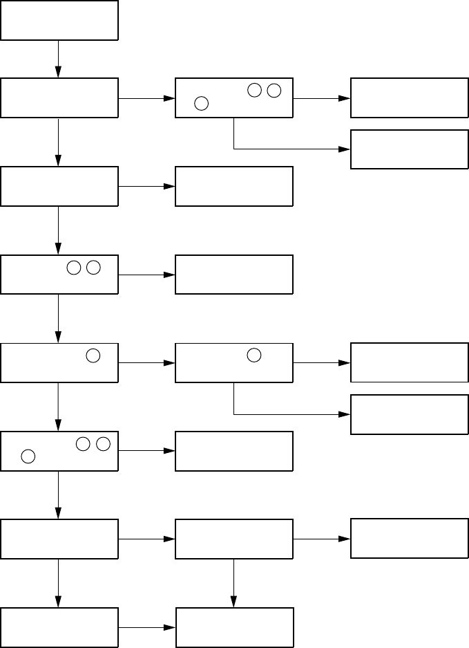
42
4. WIDE ASPECT CONVERSION CIRCUIT FAILURE ANALYSIS
PROCEDURES
4-1. Left Screen Picture Failure in Normal Mode/Double Window Modes
(No Picture, Sync Distributed)
Picture fallure
(Normal/DW mode)
Super live
mode OK?
Output at pins 5 , 6 ,
7 of PX02 OK?
LX18 adjustment
OK? Readjustment
QX01 input / output
OK?
Replace
E
2
PROM OK?
Check associated
circuit (Tr.etc). END
I
2
C bus pin 7 , 8
of PX01 OK?
Is clock at pin 47
of QX01 OK?
Signals at pins 5 , 6 ,
7 of PX02 OK?
Output at pin 3 (HD)
of PX02 OK?
Receive circuit check.
Check circuits other
than WAC unit.
Check around
of QX03.
Check around
QX02.
Replace QX01.
Check receive
circuit.
I
2
C bus line check.
N
N
N
N
Y
Y
N
N
Y
Y
N
Y
N
Y
Y
Y
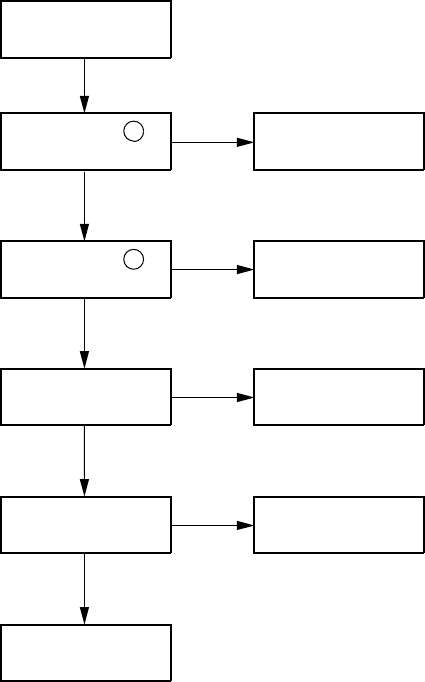
43
4-2. Raster Horizontal One
4-2-1. Adjustment Method
(1) Disconnect any video inputs
(2) Open RX-40.
(3) Connect frequency counter to QX19 emitter.
(4) Adjust LX18 until frequency reading of “28.7 MHz
± 0.5 MHz” is obtained.
Horizontal one
Output at pin 8
of PX02 OK? Check V circuit.
Output at pin 2
of PX02 OK? Check receive circuit.
Is output OK
at I2C bus?
Data initlalization OK?
Check I 2C
bus line.
Y
N
N
N
N
Y
Y
END
Y
Replace QX01.
44
1. OUTLINE
DUAL circuit performs the signal process, etc. on the sub
screen and is composed of the followings as shown in Fig. 6-
1.
• Video/color/deflection (V/C/D) process
• On-screen display (OSD) superimposing process
• Sub-screen process, memory
• Main/Sub screen picture superimposing process
• Sub screen control microprocessor
2. PRINCIPLES OF OPERATION
DUAL circuit is composed of the following functions.
(1) Double window sub screen 1/2 compression process
(2) Sub screen still process
(3) 9-screen multi-search process
(4) Main/Sub screen superimposing process by YIQ sig-
nal.
• 9-screen multi-search process
The sub screen process IC (TC9092AF) is the IC using the
programmable technology and can realize various functions
such as sub screen 1/2 compression, 9-screen multi-search,
etc. by switching the program.
The 9-screen multi-search process is carried out by selecting
the channel on the right half of the wide screen with 16:9
aspect ratio and the picture images received are projected on
the 9 screens from the upper left screen in order.
The search is carried out by approx. every 2 seconds repeat-
edly. When the next picture image is searched, the picture
image on the previous screen becomes a still picture. When
the 9 screens are finished projecting (to the picture image on
the right bottom screen), the search operation is carried out
repeatedly from the upper left screen.)
SECTION VI: DUAL CIRCUIT
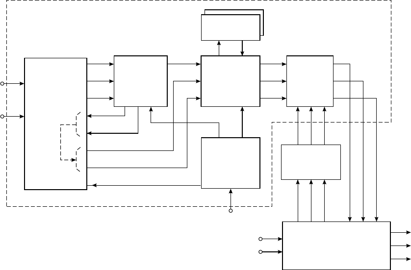
45
3. SYSTEM COMPONENT DIAGRAM OF DUAL UNIT
From tuner
SY
SC
Video/color/
deflection
process IC
µPC1832GT
R- Y
B- Y
R- Y
B- Y
Y
I
Q
Control
Y
I
Q
OSD
ON-screen
display super
impose
TC4W53F
MC74HC4053F
2M memory X2
MSM518221-30ZS
Sub screen
process IC
TC9092AF
Main/Sub
picture
superimpose
MC74HC4053F
YIQ YIQ
YIQ
I
2
C BUS
Sub screen
control micro-
processor
CXP85116B-514Q
I
2
C BUS
Wide aspect
conversion
TC9097F
G
B
R
To CR
T
V/C/D IC
TA1222N
From tuner
SY
SC
From main microprocessor
Fig. 6-1
46
4. CIRCUIT OPERATION
4-1. Video/Color/Deflection Process Section
The video/color/deflection section is shown in Fig. 6-2.
The luminance signal is supplied from pin Y08 of PY01 and
its frequency bandwidth is limited by the low pass filter (LPF)
and then input to pin 36 of V/C/D IC (VIDEO IN). The Y
signal output from pin 12 of PY01 superimposes the charac-
ter signal on the video signal by QY49 and QY44, and then
output to the sub screen process section.
QY49 and QY44 work as the analog switches. When the
screen is displayed in DW, the switch operation is not car-
ried out and the same signal as the input signal is output, and
when the 9-screen multi-search process is carried out, the
switch operation is carried out.
The OSD signal superimposes the shade of character signal
by QY49 and the character signal by QY44 on Y signal.
On the other hand, the color signal is supplied from pin Y15
of PY01, limited its frequency bandwidth by the band pass
filter (BPF) and then input to pin 34 of QY01 (COLOR IN).
The color difference signals of the demodulated signal (R –
Y) and ( B – Y) are output from pins 13 and 14 of QY01. In
the same way as the Y signal, the (R – Y) and (B – Y) signals
are superimposed on the character signal with OSD signal
by QY44.
The GBR matrix circuit which converts the Y, R – Y and B –
Y signals into three primary color signal of G, B and R is
used to convert the (R – Y) and (B – Y) signals into I and Q
signals.
In the GBR matrix circuit, each G, B and R output is output
as G – Y, B – Y and R signals when the Y signal is not input.
Then the B – Y signal is converted to Q signal, R – Y to I
signal pseudically by turning the phase by an angle of 33°.
Thus, R – Y and B – Y signals are input to pins 18 and 19 of
QY01, and the output signals from pins 23 and 24 are devel-
oped as the I and Q converted signals pseudically. The am-
plitude of the signals is amplified by 6 dB amplifier of QY23
and the signals are output to the sub screen process section.
Since the sync signal is added to the luminance signal, the
signal is input to pin 39 of QY01 (SYNC SEP IN) and the
sync signals of HD and VD are output to pins 10 and 11 of
QY01. The HD signal is waveshaped by QY42.
The HD signal (WHD1, WHD2) is used as the horizontal
pulse for sub screen write and the VD signal (WVD) is as the
vertical pulse for sub screen write in the sub screen process
section.
In the sub screen microcomputer section, various kinds of
control signals (brightness, density, hue, etc.) are output from
the sub screen control microprocessor QY91 and the signals
are used for the level matching adjustment. So the setting for
the sub screen cannot be made by the user. Furthermore, the
OSD signal for OSD superimposing is output.
The sub screen process IC control program is stored in the
nonvolatile memory of the sub screen control microproces-
sor QY91 in order to control the sub screen process IC
(TC9092AF), and the data is sent via I2C bus.
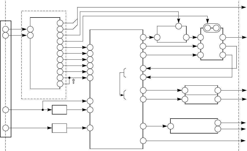
47
Y13
Y14
SCL
SDA
Y08
PIP VIDEO
Y15
PIP C
L.P.F
B.P.F
49
47
SCL2
SDA2
50SCLP
48SDAP
46BLK
43B
53COL
54TIN
51S.COL
52CON
62fsc SEL
61PAL/NTSC
23.58
20 COLOR
21 TINT
37 SUB COL.
38 CONTRAST
41 fsc SELECT
42 PAL/NTSC
Control
39 SYNC SEPA
IN
36 VIDEO IN
34 CHROMA IN
Sub screen microprocessor section
QY91 CXP85116B-514Q
Sub screen control
microprocessor
V/C/D IC
QY01 µPC1832GT
12Y OUT
13R-Y OUT
14B-Y OUT
18R-Y IN
19B-Y IN
23R OUT(I)
24B OUT(Q)
5
71
OSD
superimpose
OSD
superimpose
10HD OUT
11VD OUT
1Waveform
shape
13
5
1Q
2Q
1A
WHD2
WHD1
WVD
I
Q
3
3
1
1
6dB. Amp
To Sub screen process section
I
2
C BUS(SCL,SDA)
QY49
TC4W53F
911
12
5
2
14
4
15
Signal reception
circuit
PY01 OSD
OSD
6dB. Amp
QY22 MM1031XMR
QY23 MM1031XMR
QY42 TC74HC123AF
QY44
MC74HC4053F
Y
Fig. 6-2
48
4-2. Sub Screen Process Section
The sub screen process section is shown in Fig. 6-3.
The Y, I and Q signals from the video/color/deflection pro-
cess section are limited in their frequency bandwidth by the
LPF in the prceeding stage and input to pins 6, 13 and 15 of
QY03.
The frequency of 18.5 MHz generated by LY102 is multi-
plied by 1/2 inside QY03. The Y signal is sampled by 9.25
MHz and the I and Q signals are sampled by 4.63 MHz (1/2
frequency to multiplex) and then the signals are converted
into 8-bit digital signals.
The horizontal sync signal WHD (the signal mixed with
WHD1 and WHD2 by QY43) for writing input to pins 21
and 20 of QY03 and the vertical sync signal WVD for trig-
ger writing on the field memory QY10 and QY11.
Fig. 6-3 Sub screen process section
6
13
15
79
80
20
21
24
25
77
75
72
73
95
100
97
70
48
32
51
65
Y IN
R-Y IN
B-Y IN
SCL
SDA
FVS
FHS
OSCSI
OSCSO
FVM
FHM
OSCMI
OSCMO
L.P.F
L.P.F
L.P.F
Y
I
Q
I
2
C BUS (SCL, SDA)
WVD
WHD2 1
24
OR
circuit
WHD1 WHD
QY43
TC7S32F
LY102
LY101
PY01
RVD
RHD
YS
Signal reception circuit Video/color/deflection process section
QY03 TC9092AF
Sub screen process IC
Y OUT
R-Y OUT(I)
B-Y OUT(Q)
YS OUT
MWD 0
MWD15
MRD 0
MRD15
Y
I
Q
L.P.F
L.P.F
L.P.F
YS
QY10, QY11
MSM518221-30ZS
2M
memory
Date out
To Main/Sub pictore superimposing
process section
Date in
Y11
Y12
Y01
The horizontal sync signal RHD for reading-out and the ver-
tical sync signal RVD for reading out input to pins 75 and 77
of QY03 trigger the reading at 18.0 MHz which is created
by 2/3-multiplying 27.0 MHz developed in LY101and then
output as the analog signal.
The Y, I and Q signals converted for the sub screen are out-
put from pins 95, 100 and 97 of QY03. The output signals
are used for the input signals compressed by 1/2 in the hori-
zontal direction in the double window mode and for the in-
put signal compressed by 1/6 in the horizontal direction and
by 1/3 in the vertical direction in 9-screen multi-search mode.
Then the signals are smoothed by the LPF in the next stage
then input to the main/sub screen superimposing section.
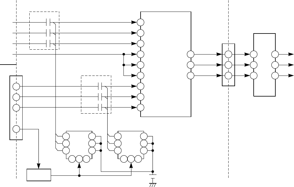
49
4-3. Main/Sub Screen Superimposing Section
In normal mode (with only the main screen picture displayed),
the YS signal voltage always goes low and the Y, I and Q
signals from the digital unit are developed at pins 15, 4 and
14 of QY48.
The Y, I and Q signals for the main/sub screens superim-
posed are developed at pins Y05, Y06 and Y04 of PY01 and
then supplied to the receive circuit.
The Y, I and Q signals for the main/sub screens superim-
posed inside the receive circuit are entered to pins 53, 51 and
52 of Q501 (TA1222N) and then fed to CRT. The video
signal is processed in Q501 without distinguishing the sig-
nals for main and sub screens, so the high picture quality can
be obtained equally for both the screens.
CY231
CY230
CY232
CY239
CY240
CY238
Y
I
Q
YS
YD
ID
QD
SCP
3
2
1
4
Clump capacitor
Clump capacitor
3
9
1
4
8
2
Analog
SW
5613
QY46
TC74HC4066AF
Analog
SW
QY47
TC74HC4066AF
5613
3
9
1
4
8
2
Waveform
shape
Clump
pulse Constant voltage
source E
From Sub screen
process section
Signal reception
circuit
Signal reception
circuit
QY48 MC74HC4053
1IY (Y IN)
3 IZ (I IN)
13 IX (Q IN)
11 A
10 B
9C
2OY (Y IN)
5 OZ (I IN)
12 OX (Q IN)
15Y COM (Y OUT)
4Z -COM (I OUT)
14X-COM (Q OUT)
Y05
Y06
Y04
53
51
52
43
42
41
R
G
B
Y
I
Q
YOUT
I
Q
PY01
Q501
To CRT
Main/Sub picture
superimpose
PY02
TA1222N
Fig. 6-4 Main/Sub screen superimposing section
The main/sub screen superimposing section is shown in Fig.
6-4.
The sub screen Y, I and Q signals sent from the sub screen
process section and the main screen Y, I and Q signals sent
from the digital unit through the receive circuit and etnered
pins 3, 2, and 1 of PY02 are clamped at a same electrical
potential and the former are fed to pins 1, 3, 13 and the latter
fed to pins 2, 5 and 12 of QY48.
The clamp circuit contains a clamp pulse waveshaping SCP
at pin 4 of PY02, analog switches for ever-voltage source E,
QY46 and QY47 and clamp capacitors CY230 ~ CY232,
CY238 ~ CY240.
QY48 is an analog switch to feed the Y, I and Q signals for
either sub screen or main screen to pins 15, 4 and 14 by the
YS signal voltage fed to pins 9, 10 and 11. When the YS
signal develops high, QY48 selects the signals for the sub
screen and when low, QY48 selects the signals for the main
screen. Consequently, the signals for both the main and sub
screens are superimposed each other.
50
5. TERMINAL FUNCTION, DESCRIPTION AND BLOCK DIAGRAM OF
MAIN IC
42
Mode SW Separate / Composite SW,
ACC amp., Sub color control
41 40 39 38 37 36 35 34 33 32 31 30 29 28 27 26 25 24 23 22
1 2 3 4 5 6 7 8 9 10 11 12 13 14 15 16 17 18 19 20 21
3.58 / 4.43
PAL / NTSC
Sync. sepa.
V. filter
H. sync det.
H / V count
Clamp
fsc
trap
Separate / composite SW
321H VCO AFC wave
form det.
Delay Contrast
control
HD, VD, blanking pulse,
killer output Y, R-Y, B-Y output
L P F
R-Y, B-Y
demodulation
APC killer wave form det.
IDENT D det.
PAL / NTSC
matrix
Tint control
Color control
RGB output
3.58MHz / 4.43MHz
VCXO. PAL SW
Filter
fH Adj.
fsc BPF
Y, R-Y, B-Y input clamp
BGR
Clamp pulse
1MΩ
0.22µF1.8 KΩ
18pF
4.43MHz 3.58MHz
18
pF
0.47µF
6.8KΩ
4700pF0.22µF
1MΩ
1µF
+
+
22µF
0.1µF
+
Separate
/ color
1000pF
Separate / composite SW
Vcc
20kΩ
0.22µF
20kΩ
Vcc Vcc
0.1µF
Contrast
control
0.1µF
Sub color
control
+
4.7µF
100Ω
180kΩ
1500pF
43kΩ
CVBS
2.2kΩ
220pF
820pF
500pF
330Ω
0.015µF
4.7µF
+
8.2kΩ
2.7kΩ
50 / 60
0.1µF
22µF
Killer det. BLK HD VD Y R-Y B-Y
Vcc
Vcc
0.22µF0.22µF0.22µF
0.1µF
Color control
Tint control
20kΩ
0.1µF
22µF
+
R-Y B-Y
20kΩ
+
1.8 KΩ
+1
0.1µF
Fig. 6-5 QY01 mm
mm
mPC1832GT internal block diagram
51
1
2
3
4
5
6
7
8
9
10
11
12
13
14
15
16
17
18
19
20
21
42
41
40
39
38
37
36
35
34
33
32
31
30
29
28
27
26
25
24
23
22
PAL/NTSC SW
fsc SW
H. sync det. filter
Sync sepa input
Contrast control
Sab color control
Composite video signal inpu
t
Power supply (color)
Separati color input
GND (color)
ACC filter
I
o
. filter
Color APC filter
f
sc
VCO input (4.43MHz)
f
sc
VCO input (3.58MHz)
f
sc
VCO output
Color killer filter
B output
G output
R output
Clamp pulse input
32f
m
VCO felter 1
32f
m
VCO felter 1
32f
m
VCO felter 1
H.AFC filter
GND (sync)
fv 50/60 SW
Power supply (sync)
Color killer output
Blanking pulse output
HD pulse output
VD pulse output
Y output
R-Y output
B-Y output
GND (video)
Y input
Power supply (video)
R-Y input
B-Y input
Color control
Tint control
µPC1832GT
Fig. 6-6 QY01 mm
mm
mPC1832GT pin layout
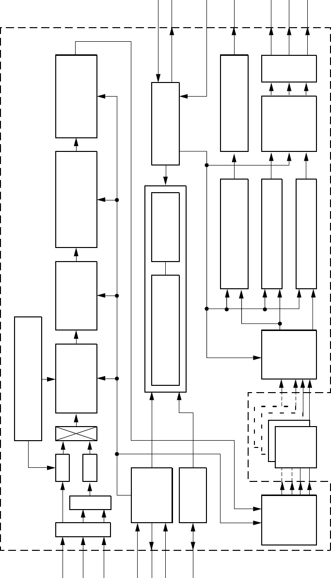
52
Fig. 6-7 QY03 TC9092AF internal block diagram
CLAMP
MPX
AD
AD
Sub screen
video input
FILTER FACTOR OPERATION/
GENERATION (KGEN)
HORIZONTAL
INTERPORATION
FILTER (HFB)
HORIZONTAL
FOLD SIGNAL
ELIMINATING
FILTER (HFA)
VERTICAL FOLDED
ELIMINATION
INTERPORATION FILTER
(1H MEMORY (12BIT)) (V)
YC DELAY
ADJUSTMENT
BETWEEN Y/C
(DAJA)
CLOCK
GENERATION
(SUB) CLOCK GENERATION
(MAIN)
PROGRAM DATA MEMORY
(16k BIT + 3k BIT)
CU
(CONTROL UNIT)
I
2
C
INTERFACE
I
2
C
DATA
REARRANGE
MENT
(W)
PICTURE
MEMORY
(2M BIT) SUB SAMPLE PIT FILLING (C)
DELAY ADJUSTMENT (DAJB)
TELTEXT DETECTION (J)
1H MEMORY (11BIT)
FRAME SIGNAL
GENERATION
(WAKU)
FRAME
SIGNAL
MULTIPLEX
SW
DA
Y
LC
LC
H, V (Sub)
H, V (Main)
Ys
Y
R-Y
B-Y
R-Y
B-Y
DATA
REARRANGE
MENT
(R)
53
MRD1
MRD2
MRD3
MRD4
MRD5
MRD6
MRD7
MRD8
MRD9
MRD10
RMD11
RMD12
MRD13
MRD14
MRD15
RE
RSTR
CKR
CKRI
YSOUT
VSS
OSCMI
OSCMO
VDD
FHM
HFHM
FVM
VSS
SCL
SDA
SDAINO
VSS
PROMDI
PROMCK
PROMRES
ME
RESET
TEST1
TESTAD
VDD
NC
DAVREFY
DABIAS1
DAVDD
YOUT
DAVSS
RYOUT
DAVREFC
DAVDD
BYOUT
MRD0
VDD
MWD0
MWD1
MWD2
MWD3
MWD4
MWD5
MWD6
MWD7
VSS
MWD8
MWD9
MWD10
MWD11
MWD12
MWD13
MWD14
MWD15
RSTW
WE
IE
CKW
VDD
VSS
OSCSO
OSCSI
VDD
NFHS
FHS
FVS
VDD
VSS
ADDVSS
ADDVDD
RYIN
ADBIAS
RYIN
ADVREFC
ADVDD
CLAMPC
ADVSS
CLAMPY
ADVSS
YIN
ADVREFY
ADVDD
DABIAS2
DABIAS3
DAVSS
TC9092AF
(TOP VIEW)
30
29
28
27
26
25
24
23
22
21
20
19
18
17
16
15
14
13
12
11
10
9
8
7
6
5
4
3
2
1
51
52
53
54
55
56
57
58
59
60
61
62
63
64
65
66
67
68
69
70
71
72
73
74
75
76
77
78
79
80
81 82 83 84 85 86 87 88 89 90 91 92 93 94 95 96 97 98 99 100
50 49 48 47 46 45 44 43 42 41 40 39 38 37 36 35 34 33 32 31
Fig. 6-8 QY03 TC9092AF pin layout

54
No. Pin name I/O Pin function
1 DAVSS D/A GND
2 DABIAS3 D/A bias condenser connection terminal
3 DABIAS2 D/A bias condenser connection terminal
4 ADVDD A/D power supply
5 ADVREFY I A/D Y reference condenser connection terminal
6 YIN I A/D Y input terminal
7 ADVSS A/D GND
8 CLAMPY Y clamp bias condenser connection terminal
9 ADVSS A/D GND
10 CLAMPY C clamp bias condenser connection terminal
11 ADVDD A/D power supply
12 ADVREFC I A/D reference condenser connection terminal
13 RYIN I A/D R – Y input terminal
14 ADBIAS A/D bias condenser connection terminal
15 BYIN I A/D B– Y input terminal
16 ADDVDD A/D digital power supply
17 ADDVSS A/D digital GND
18 VSS Digital GND
19 VDD Digital power supply
20 FVS I Sub screen vertical sync signal input
21 FHS I Sub screen horizontal sync signal input
22 NFHS I Sub screen horizontal sync signal reversing input
23 VDD Digital power supply
24 OSCSI I Oscillator connection terminal sub input
25 OSCSO O Oscillator connection terminal sub output
26 VSS Digital GND
27 VDD Digital power supply
28 CKW O Serial write clock output terminal
29 IE O Input enable output terminal
30 WE O Write enable output terminal
31 RSTW O Reset write output terminal
32 MWD15 O Data output terminal
33 MWD14 O Data output terminal
34 MWD13 O Data output terminal
35 MWD12 O Data output terminal
36 MWD11 O Data output terminal
37 MWD10 O Data output terminal
38 MWD9 O Data output terminal
39 MWD8 O Data output terminal
40 VSS Digital GND
41 MWD7 O Data output terminal
42 MWD6 O Data output terminal
43 MWD5 O Data output terminal
44 MWD4 O Data output terminal
45 MWD3 O Data output terminal
46 MWD2 O Data output terminal
47 MWD1 O Data output terminal
48 MWD0 O Data output terminal
49 VDD Digital power supply
50 MRD0 I Data input terminal
Table 6-1 QY03 TC9092AF pin list (No. 1)

55
No. Pin name I/O Pin function
51 MRD1 I Data input terminal
52 MRD2 I Data input terminal
53 MRD3 I Data input terminal
54 MRD4 I Data input terminal
55 MRD5 I Data input terminal
56 MRD6 I Data input terminal
57 MRD7 I Data input terminal
58 MRD8 I Data input terminal
59 MRD9 I Data input terminal
60 MRD10 I Data input terminal
61 MRD11 I Data input terminal
62 MRD12 I Data input terminal
63 MRD13 I Data input terminal
64 MRD14 I Data input terminal
65 MRD15 I Data input terminal
66 RE O Read enable output terminal
67 RSTR O Read reset output terminal
68 CKR O Serial read clock output terminal
69 CKRI I Memory read clock input
70 YSOUT O Ys signal output terminal
71 VSS Digital GND
72 OSCMI I Oscillator connection terminal main input
73 OSCMO O Oscillator connection terminal main output
74 VDD Digital power supply
75 FHM I Main screen horizontal sync signal input
76 NFHM I Main screen horizontal sync signal reversing input
77 FVM I Main screen vertical sync signal input
78 VSS Digital GND
79 SCL I I2C CK input terminal
80 SDA BID I2C data I/O terminal
81 SDAINO O I2C data direction output terminal, Test output terminal
82 VSS Digital GND
83 PROMDI I ROM data input terminal
84 PROMCK O ROM clock output terminal
85 PROMRES O ROM RESET output terminal
86 ME I MEMORY polarity control input terminal
87 RESET I RESET input terminal
88 TEST1 I TEST input terminal
89 TESTAD I AD/DA TEST input terminal
90 VDD Digital power supply
91 NC
92 DAVREFY I D/A Y reference voltage input terminal (4V)
93 DABIAS1 D/A bias condenser connection terminal
94 DAVDD D/A power supply
95 YOUT O D/A Y output terminal
96 DAVSS D/A GND
97 RYOUT O D/A R – Y output terminal
98 DAVREFC I D/A C reference voltage input terminal (3V)
99 DAVDD D/A power supply
100 BYOUT O D/A B – Y output terminal
Table 6-2 QY03 TC9092AF pin list (No. 2)
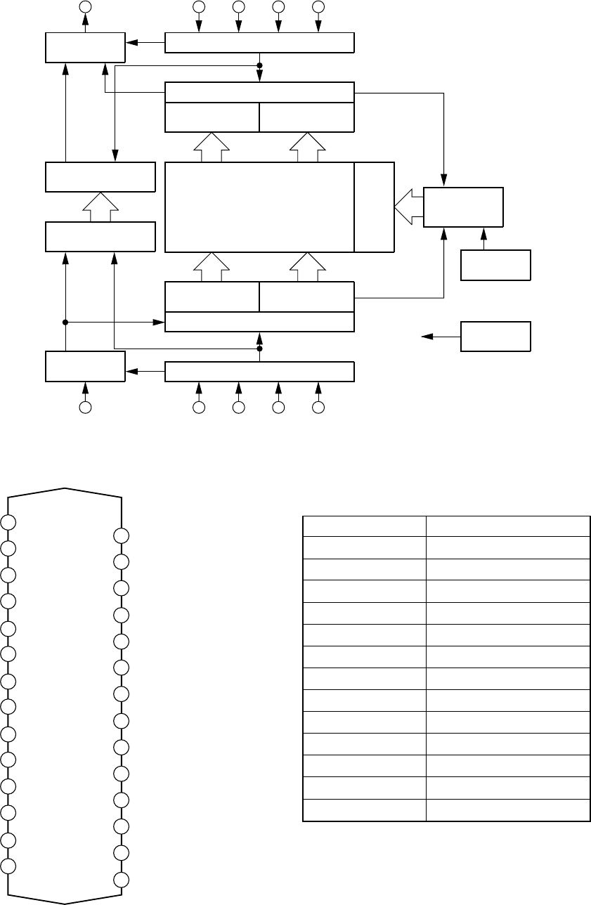
56
Dout (X8) OE RE RSTR SRCK
Data - out
buffer (X8)
Serial Read Controller
512 Word serial read register (X8)
Read line buffer
Low-Half (X8)
Read line buffer
High-Half (X8)
71 Word
Sub-register (X8)
71Word
Sub-register (X8)
256K (X8)
Memory
Array
X
De-
coder
Read/Write
and refresh
controller
Clock
oscillator
Write line buffer
Low-Half (X8)
Write line buffer
High-Half (X8)
512 Word serial write register (X8)
256 (X8) 256 (X8)
256 (X8) 256 (X8)
Serial Write Controller
Data - in
Buffer (X8)
VB3
Generator
Din (X8) IE WE RSTW SWCK
WE
Din0
Din2
Vcc
Din5
Din7
SWCK
NC
OE
Dout6
Dout4
Dout3
Dout1
RSTR
IE
Din1
Din3
Din4
Din6
RSTW
NC
RE
Dout7
Dout5
Vss
Dout2
Dout0
SRCK
28PIN ZIP
1
3
5
7
9
11
13
15
17
19
21
23
25
27
2
4
6
8
10
12
14
16
18
20
22
24
26
28
Terminal name Function
SWCK Serial write clock
SRCK Serial read clock
WE Write enable
RE Read enable
IE Input enable
OE Output enable
RSTW Reset write
RSTR Reset read
Din 0 – 7 Data input
Dout 0 – 7 Data output
VCC Power supply (+5V)
VSS Ground (0V)
NC Not connected
Fig. 6-9 QY10/QY11 M518221-30ZS internal block diagram
Fig. 6-10 QY10/QY11 M518221-30ZS pin layout
57
2-2. Circuit Description
Fig. 7-1 shows a block diagram of the YCS circuit.
(1) A video signal sent through the AV switching circuit
passes the input terminal (DG) and enters the YCS unit.
(2) The video signal entered is limited in its band width in
passing through an aliasing distortion elimination LPF
consisting of LZ22, etc. , and then enters pin 56 of
QZ01.
(3) At the same time, a fsc (3.58 MHz) signal being oscil-
lated in the video signal color IC (Q501, AN1222AN)
is fed to pin 28 of QZ01 and converted into a 4fsc
(14.32 MHz), a drive clock frequency inside the IC.
(4) The video signal entered pin 56 of QZ01 is processed
inside the IC and a luminance (Y) signal is developed
at pin 48 of QZ01 and the color signal at the pin 51.
(5) The Y signal developed at pin 48 of QZ01 passes a
LPF (LZ20, etc.) which eliminates the clock signal
component, amplified by a 6dB amplifier QZ21, etc.
and comes out from the DC terminal as the Y signal.
(6) At the same time, the color signal developed at pin 51
of QZ01 passes a LPF (LZ21, etc.) which eliminates
the clock component, amplified by 6dB by QZ23, etc.
and comes out from DD terminal through a buffer of
QZ24 as the C signal.
(7) QZ04 is generating a clock signal used to read and
write the digital data between QZ03 and QZ04 based
on the video signal.
(QZ16 emitter: 28.6 MHz ± 0.2 MHz, adjusted by
LZ25.)
1. OUTLINE
The 3D YC separation circuit uses a comb filter with a frame
memory and ideally separates the Y (luminance) and color
signal for still parts of a picture, thus providing a clean pic-
ture without:
(1) Dot interference causing at border areas of color pic-
tures.
(2) Excess color in vertical direction.
However in a moving picture, as the picture moves between
the first and second frames, good separation is not obtained.
To prevent this, a motion detection is carried out in the 3D
YC separation (hereafter called YCS) unit (PB6347). When
a picture moving is detected a 2D YC separation using a
line memory is switched in and when not detected or for a
still picture 3D YC separation is switched in, thereby cor-
recting defects both the systems have and performing the
ideal YC separation. The motion detection accuracy and
smoothness of the switching, etc. are controlled through the
IIC bus.
After completion of the Y and S signal separation, a vertical
contour correction is carried out for the Y signal.
2. CIRCUIT DESCRIPTION
2-1. Configuration
The YCS unit consists of a YC separation IC (QZ01,
TC9086F) which plays major roles, 2 Mbyte field memory
(QZ02, QZ03), clock generation IC (QZ04, TA8667F), and
peripheral circuits (LPF, AMP,emitter followers, etc.).
Of the above circuit blocks, QZ01 (TC9086F) includes an
A/D converter, D/A converter, clamp circuit, 4fsc PLL cir-
cuit, 1 line dot countermeasure circuit, vertical contour cor-
rection logic circuit, etc. and provides a high separation with
less variations.
SECTION VII: 3-DIMENSION Y/C SEPARATOR CIRCUIT
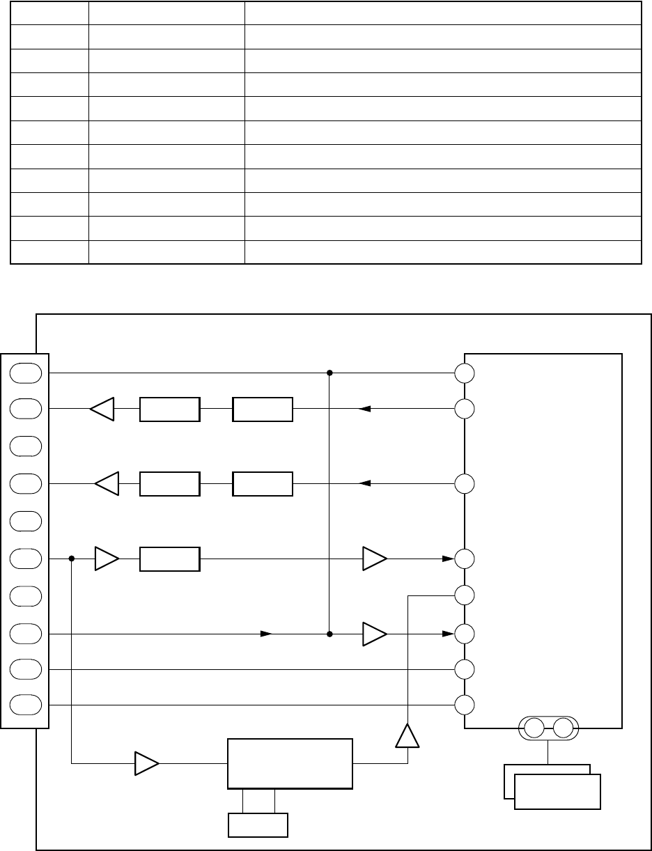
58
• Terminal description (PZ01)
No.
DH
DC
DE
DD
DB
DG
DA
DF
DI
DJ
Signal name
Comb through
Y-Comb
9V
C-Comb
GND
V-AV
5V
fsc
SDA1
SCL1
Voltage
Comb through pulse for ED2 ID signal period (V frequency), 5V
2V(p-p)
+9V ± 0.5V
0.6V(p-p) at burst
GND
2V(p-p)
+5V ± 0.5V
0.4V(p-p), 3.58 MHz
IIC bus data, 5V
IIC bus clock, 5V
Fig. 7-1 3-dimension Y/C separator unit block diagram
DH
DC
DD
DG
DF
DI
DJ
DE
DB
DA
36
48
51
56
28
20
19
AMP LPF
AMP LPF
LPF
QZ21 LZ20 etcQZ22
QZ23 LZ21 etc
LZ23 etc
QZ24
KILL
YOUT
COUT
CVIN
FSC
DATA
SLK
PZ01 QZ01 TC9090N
QZ06
QZ02
QZ03
QZ04 TA8667F
LZ25
28.6MHz
8FS2N
QZ05
QZ07
QZ14
QZ16
64
100
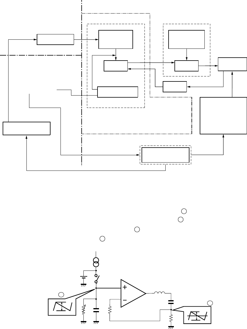
59
1. OUTLINE
The sync separation circuit, V pulse circuit, and blanking
circuit are provided inside Q501 (TA1222AN). The saw tooth
wave generation circuit and amplifier (V driver circuit) are
provided inside Q302 (TA8859AP).
Q301 (LA7833S) contains the pump up circuit and the output
circuit. V screen position switching function which lowers
the V raster position by flowing an opposite DC current into
the deflection yoke. This circuit is used selecting SUBTITLE
and CINEMA MODE.
MICROPROCESSOR
SYNC SEP.V PULSE/
BLANKING
PULSE DELAY
SAWTOOTH
WAVE
GENERATOR
AMP
Q302 TA8859AP
CONTROL CIRCUIT
Q301 LA7833S
PUMP UP
CIRCUIT
OUTPUT
FEEDBACK
DEFLECTION
YOKE
V-RASTER SHIFT
CIRCUIT
AUTO LIVE
MICROPROCESSOR
( I
2
C BUS)
( I
2
C BUS)
Q501 TA1222AN
V/C/D LSI
WAC
V-BLK
Fig. 8-1
Vp S: Switch Differential
amplifier
C2
R3
V2
c
R1 C2 R2
a
V1
L
A
1-1. Theory of Operation
The purpose of the V output circuit is to provide a sawtooth
wave signal with good linearity in V period to the deflection
yoke.
When a switch S is opened, an electric charge charged up to
a reference voltage VP discharges in an constant current rate,
and a reference sawtooth voltage generates at point a .
This voltage is applied to (+) input (non-inverted input) of
an differential amplifier, A. As the amplification factor of A
is sufficiently high, a deflection current flows so that the
voltage V2 at point c becomes equal to the voltage at point
a .
Fig. 8-2
SECTION VIII: VERTICAL OUTPUT CIRCUIT
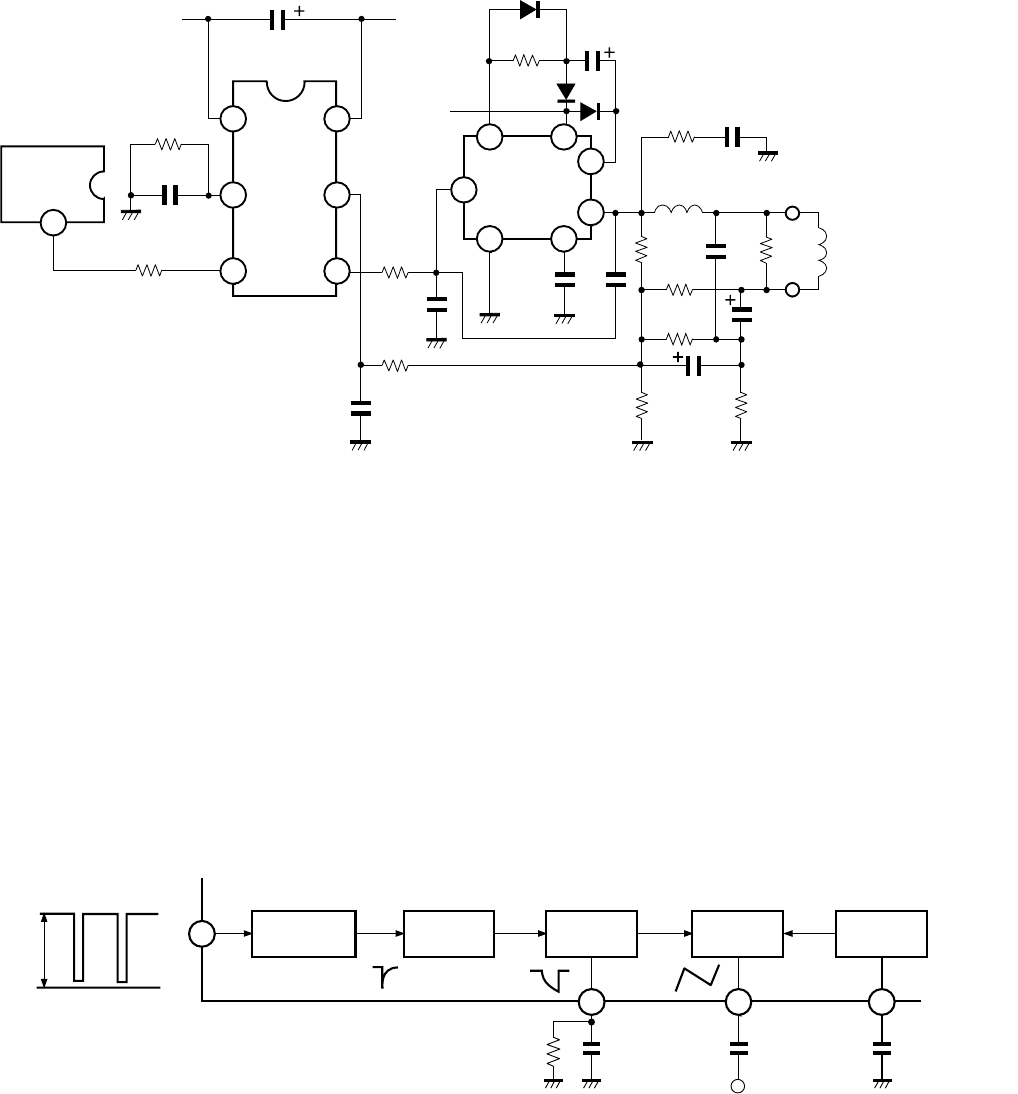
60
2. V OUTPUT CIRCUIT
2-1. Actual Circuit
31
15
14
13
3
6
8
76
4
15
2
3
C322
R329
Q501 C321
R320
Q302
+9V
D309
+35V
R301
R330
C319
C314
Q301
C309 C311
R308 C308
D301 C313
R303
L301 R336
R307 L462+L463+L464
R306
R313 C306
R305
C305
R304
C307
D308
Fig. 8-3
2-2. Sawtooth Waveform Generation
2-2-1. Circuit Operation
The sawtooth waveform generation circuit consists of as
shown in Fig. 8-4. When a trigger pulse enters pin 13, it is
differentiated in the waveform shape circuit and only the
falling part is detected by the trigger detection circuit, to the
waveform generation circuit is not susceptible to variations
of input pulse width.
13
14 15 16
5Vp
DC=0V
WAVEFORM
SHAPE
TRIGGER
DET.
PULSE
GAIN V. LAMP AGC
+
+9V
R329 C321 C322 C323
Fig. 8-4
The pulse generation circuit also works to fix the V ramp
voltage at a reference voltage when the trigger pulse enters,
so it can prevent the sawtooth wave start voltage from
variations by horizontal components, thus improving
interlacing characteristics.
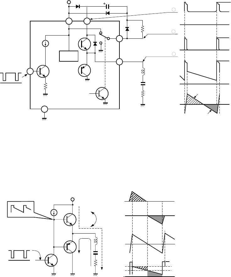
61
2-3. V Output
2-3-1. Circuit Operation
The V output circuit consists of a V driver circuit Q302,
Pump-up circuit and output circuit Q301, and external circuit
components.
(1) Q2 amplifies its input fed from pin 4 of Q301, Q3, Q4
output stage connected in a SEPP amplifies the cur-
rent and supplies a sawtooth waveform current to a
deflection yoke.
Fig. 8-6
Q3 turns on for first half of the scanning period and
allows a positive current to flow into the deflection
yoke (Q3 ® DY ® C306 ® R305 ® GND), and Q4
turns on for last half of the scanning period and allows
a negative current to flow into the deflection yoke
(R305 ® C306 ® DY ® Q4). These operations are
shown in Fig. 8-5.
V 3
V 7
V 2
1
4
2
7
36
Q2
Q4
BIAS
CIRCUIT
Q3
Q301
+35V
D301 C308
D308
D309 R308
DY
C306
R305 Q3 ON
Q4 ON
GND
GND
63V
35V
GND
35V
GND
63V
+
(2) In Fig. 8-6 (a), the power Vcc is expressed as a fixed
level, and the positive and negative current flowing
into the deflection yoke is a current (d) = current (b) +
(c) in Fig. 8-6, and the emitter voltage of Q3 and Q4 is
expressed as (e).
(3) Q3 collector loss is i1 x Vce1 and the value is equal to
multiplication of Fig. 8-6 (b) and slanted section of
Fig. 8-6 (e), and Q4 collector loss is equal to multipli-
cation of Fig. 8-6 (c) and dotted section of Fig. 8-6
(e).
Fig. 8-5
Power Vcc
Q3
Q4
Q2
i1
i2
Vce 1
GND (b) Q3 Collector current i1
GND (c) Q4 Collector current i2
GND (d) Deflection yoke current i1+i2
Vp
Vcc
1/2 Vcc
GND
(e)
(a) Basic circuit
62
(4) To decrease the collector loss of Q3, the power supply
voltage is decreased during scanning period as shown
in Fig. 8-7, and VCE1 decreases and the collector loss
of Q3 also decreases.
Fig. 8-7 Output stage power supply voltage
(5) In this way, the circuit which switches power supply
circuit during scanning period and flyback period is
called a pump-up circuit. The purpose of the pump-up
circuit is to return the deflection yoke current rapidly
for a short period (within the flyback period) by ap-
plying a high voltage for the flyback period. The basic
operation is shown in Fig. 8-8.
Q3 Collector loss decreases
by amount of this area
Power supply
for flyback period (Vp)
Power supply
for scanning period
(Vcc)
Scanning period
Flyback period
(6) Since pin 7 of a transistor switch inside Q301 is con-
nected to the ground for the scanning period, the power
supply (pin 3) of the output stage shows a voltage of
(VCC – VF), and C308 is charged up to a voltage of
(VCC – VF – VR) for this period.
(7) First half of flyback period
Current flows into L462 + L465 + L464 ® D1 ® C308
® D308 ® VCC (+35V) ® GND ® R305 ® C306
® L462 + L463 + L464 in this order, and the voltage
across these is:
VP = VCC + VF + (VCC – VF – VR) + VF about 63V
is applied to pin 3. In this case, D301 is cut off.
(8) Last half of flyback period
Current flows into VCC ® switch ® D309 ® C308
® Q301 (pin 3) ® Q3 ® L462 + L463 + L464 ®
C306 ® R305 in this order, and a voltage of
VP = VCC – VCE (sat) – VF + (VCC – VF – VR) –
VCE (sat), about 56V is applied to pin 3.
(9) In this way, a power supply voltage of about 35V is
applied to the output stage for the scanning period and
about 63V for flyback period.
63
7
2
63
7
2
D301 C308
D308
Q301
D309
Switch
Q3
Q4
D1
L462+L463+L464
C306
R305
D301 C308
Q301
D309
Q3
Q4
D1
L462+L463+L464
C306
R305
Switch VR
Last half
(a) Scanning period (b) Flyback period
First half
+
D308
+
R308 R308
Fig. 8-8
63
2-4. V Linearity Characteristic Correction
2-4-1. S-character Correction
(Up-and Down-ward Extension Correction)
A parabola component developed across C306 is integrated
by R306 and C305, and the voltage is applied to pin 6 of
Q302 to perform S-character correction.
2-4-2. Up-and Down-ward Linearity Balance
A voltage developed at pin 2 of Q301 is divided with resistors
R307 and R303, and the voltage is applied to pin 6 of Q301
to improve the linearity balance characteristic.
3. PROTECTION CIRCUIT FOR V DEFLECTION STOP
When the deflection current is not supplied to the deflection
coils, one horizontal line appears on the screen. If this
condition is not continued for a long time, no trouble will
occur in a conventional TV. But in the projection TV, all the
electron beams are directly concentrated at the fluorescent
screen because of no shadow mask used, and burns out the
screen instantly.
To prevent this, the stop of the V deflection is detected when
the horizontal one line occurs, and the video signals are
blanked out so that the electron beams are not emitted.
When the V deflection circuit is operating normally, a
sawtooth wave voltage is obtained across (R305), so Q350
repeats on-off operation in cycle of V sync. In this case, the
collector voltage of Q35 is set to develop less than (12V-
VBE (Q351)) with R352 and C350 as shown in Fig. 8-9.
Accordingly, Q351 and Q353 are continuously turned on.
As a result, diode D354 is turned off, giving no influence on
the blanking operation.
C306
2
L462+L463+L464
R350
R305
Q350
R354
C350
R352
Q351
12V
D354
D353
BLANKING
CIRCUIT
R351
9V
Q353
Q301
D350
Next, when the V deflection stops, the voltage across (R305)
does not develop, so Q350 turns off, and both the Q351 and
Q353 are turned off. Then, the picture blanking terminal
pin 13 of ICA05 is set to high through R354 and D354
connected to 90V power line, BLANKING CIRCUIT ON
thus cutting off the projection tubes.
Fig. 8-10
Volttage Across
R305
Q350 BASE
Q351 Collector
Q340 V
BE
12V-V
BE
(Q341)
Fig. 8-9
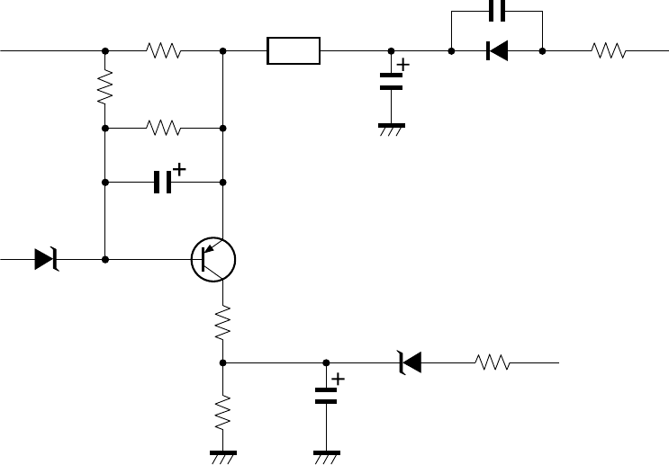
64
3-1. +35V Over Current Protection Circuit
The over current protection circuit cuts off the power supply
relay when it detects abnormal current increased in the +35V
power line due to failure of the vertical deflection circuit.
3-1-1. Theory of Operation
Fig. 8-11 shows the circuit diagram of the over current
protection circuit. When the load current of the +35V line
increases, the voltage across a resistor of T370 will also
increase.
Fig. 8-11
When the voltage increases across R370. and the voltage
developed across R371 becomes higher than the Vbs of
Q370, Q370 turns on and a voltage develops across R374
due to the collector current flowing. When this voltage
increases to a value higher than about 7V, Z801 operates,
thus cutting off the power relay. When the circuit operates, a
power LED provided will turn on and off in red.
R372
R370
R371
C370
Q370
2SA933SQ
D421
UZ22BSD
R373
R374
+35V
C310 D302
C303
R327
FBT
pin 6
C371
D370
UZ11BSB
R375
To pin 14 (GATE)
of Z801
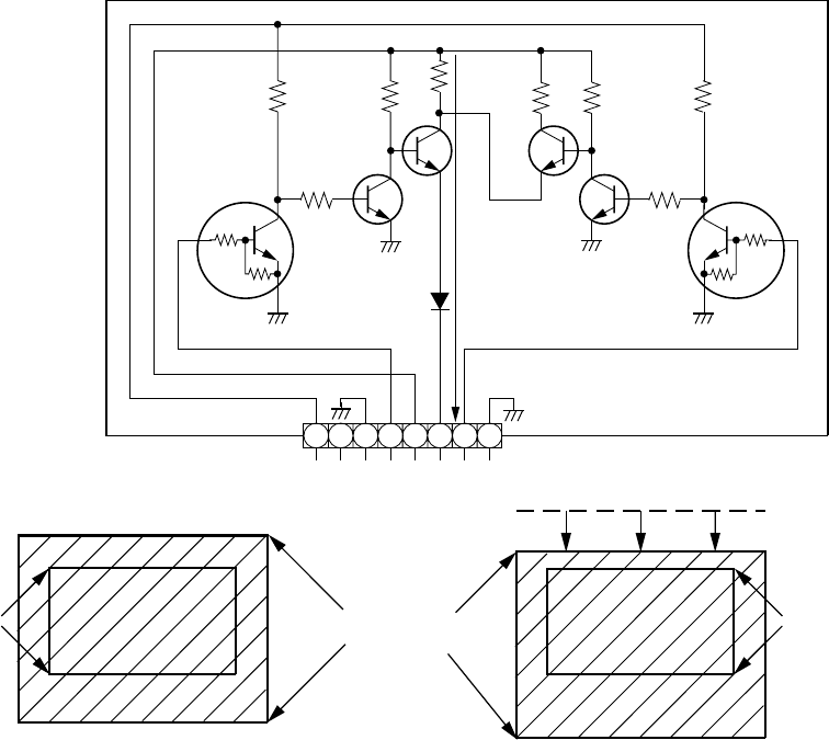
65
4. RASTER POSITION SWITCHING CIRCUIT
4-1. Outline
When the vertical screen position adjustment is carried out
on the projection TV, DC current is directly flown in the
vertical deflection yoke and the raster cannot be moved up
and down. (Because the raster is moved, the color distortion
may occur.) Accordingly, the vertical screen position
adjustment is carried out by the following method. (Only in
CINEMA and SUBTITLE mode)
V sync pulse output from Q501 sync. separation circuit is
once input to WAC, delayed and then output. The deflection
circuit operates with the delayed sync signal. The screen
upper side position moves up and down by varying the delay
time. When the vertical position adjustment is carried out
by WAC, the followings must be considered.
WAC becomes “through” except for CINEMA and
SUBTITLE mode.
The phase of the output V sync must not advance from that
of WAC input V sync. If it advances, Vertical jitter may occur
when performing the search operation and the vertical
position adjustment of a VTR.
Raster position
Nomal mode (4:3, Full, Dramatic Wide) Mode in which the opposite current
flows into D Y
(
Cinema
)
Screen
mask
position
Screen
mask
position
Fig. 8-13
So, adjust the center of the picture to the center of the screen
in advance under the output V sync delayed.
To do this, lower the raster position by flowing a DC current
to the deflection yoke in the CINEMA and SUBTITLE
mode.
The operation above is carried out by the vertical screen
position SW circuit.
4-2. Operation
When CINEMA and SUBTITLE are selected in the screen
mode, a zoom signal is input to the base of Q362 from the
autolive circuit and Q362 turns on. Then, Q363 turns off
and the base of Q364 develops H and Q364 turns on. The
inverted DC current flows into the vertical deflection yoke
from +35V power supply line.V power supply line and then
the raster moves down.
Q362
RN1204
R361
12K
Q363
2SC1815Y
Q364
2SC2023
R362
1R5.6K
R360
33K
R364
KETSU R365
1R5.6K
R367
12K
Q365
2SC1815Y
Q367
2SC2023
R366
33K
D361
S5965G
R363
2R
220
Q366
RN1204
+35V
+12V
P360
Fig. 8-12
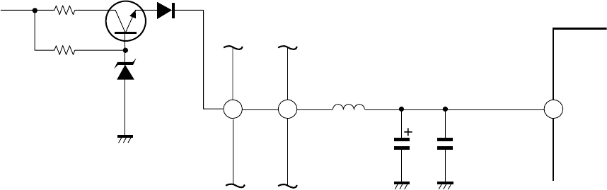
66
1. OUTLINE
The H deflection circuit works to deflect a beam from left to
right by flowing a sawtooth waveform of 15.625 kHz/15.735
kHz into the DY H deflection coil.
2. HORIZONTAL DRIVE CIRCUIT
The H drive circuit works to start the H output circuit by
applying H VCC (Q501 DEF power source) to pin 22 of
Q501 (TA1222N) and a bias to the H drive transistor Q402
at the main power on.
2-1. Theory of Operation
(1) When the power switch is on, the main power supply
of 125V starts to rise. At the same time, AF power sup-
ply 38V also rises.
(2) With 38V line risen, Q430 base voltage which is cre-
ated by dividing the audio power with R433 and D430
also rises. Then, the transistor Q430 turns on and the
H VCC is applied from the audio power line through
R432 and D431 to pin 22 of Q501.
Fig. 9-1 H drive circuit block diagram
81 81 22
R432 Q430 D431
R433 D430
BB80
BB81
L400
SIGNAL C431 C430
H Vcc
Q501
35V
3. BASIC OPERATION OF HORIZONTAL DRIVE
(2) To turn on the output transistor completely and to make
the internal impedance low, a sufficiently high, for-
ward drive voltage must be applied to the base and
heavy base current ib must be flown. On the contrary,
to completely turn off the transistor, a sufficiently high,
reverse voltage must be applied to the base.
(3) When the transistor is on (collector current is maxi-
mum) condition with the sufficiently high forward volt-
age applied to the base, the transistor can not be turned
off immediately, if a reverse base bias is applied to the
base because minority carriers storaged in the base can
not be reduced to zero instantly. That is, a reverse cur-
rent flows through an external circuit and gradually
reduces to zero. The time lag required for the base cur-
rent to disappear is called a storage time and falling
time.
A sufficient current must flow into base of the horizontal
output transistor to rapidly make it into a saturated (ON)
condition or a cut off (OFF) condition. For this purpose, a
drive amplifier is provided between the oscillator circuit and
the output circuit to amplify and to waveshape the pulse volt-
age.
3-1. Theory of Operation
(1) The horizontal drive circuit works as a so called switch-
ing circuit which applies a pulse voltage to the output
transistor base and makes the transistor on when the
voltage swings in forward direction and off in reverse
direction.
SECTION IX: HORIZONTAL DEFLECTION CIRCUIT
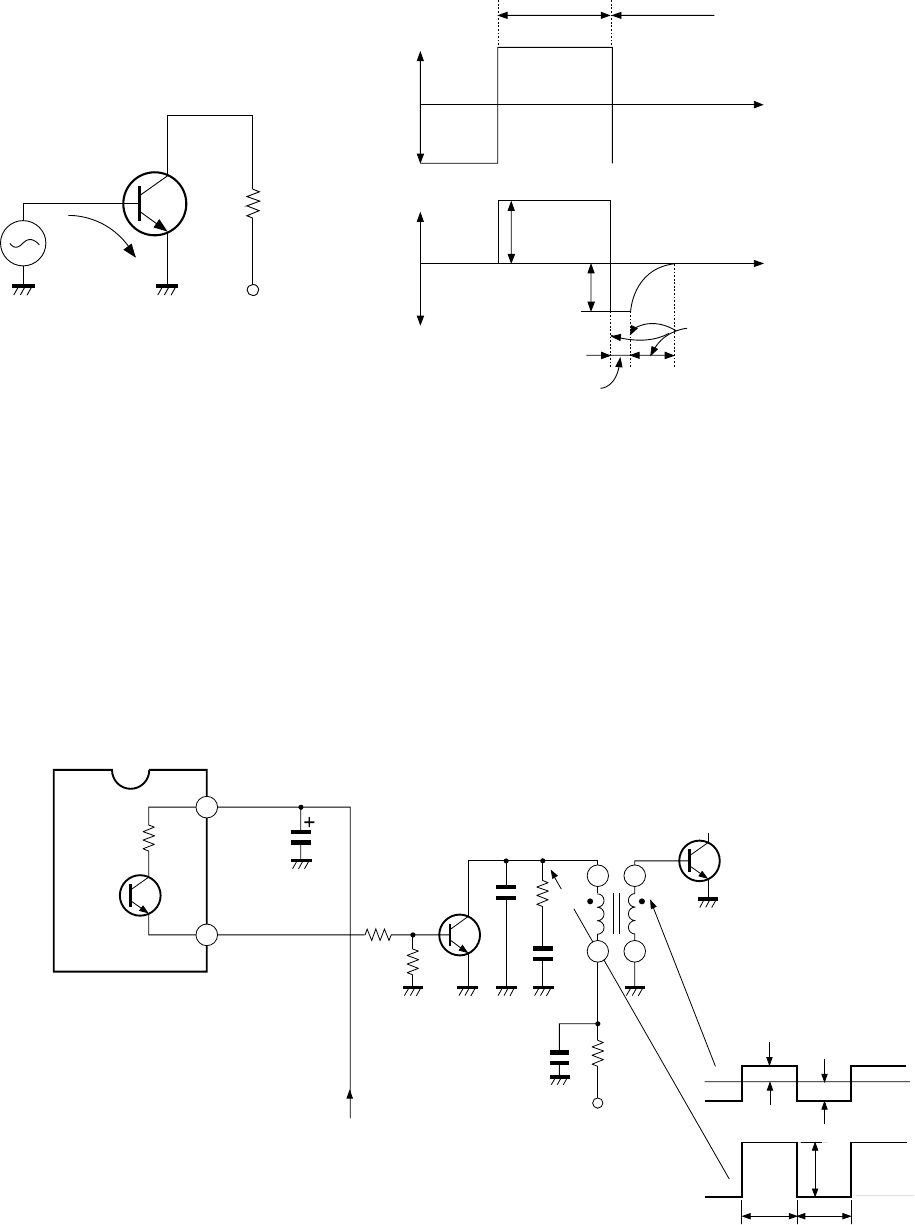
67
(4) To shorten the storage time and the falling time, a suf-
ficiently high reverse bias voltage must be applied to
allow a heavy reverse current to flow. This operation
also stabilizes operation of the horizontal output tran-
sistor.
Fig. 9-3
Fig. 9-2
3-2. Circuit Description
In the N5SS chassis, the off drive system is employed.
(1) When Q1 inside Q501 is turned on, Q402 base is for-
ward biased through 9V ® pin 22 of Q501 (H. VCC)
® pin 23 of Q501 (H. Out) ® R411/R410 resistor di-
vider, and then, Q402 collector current flows through
125V ® R416 ® T401. In this case, the H output tran-
sistor Q404 turns on with the base-emitter reverse bi-
ased because of the off drive system employed.
(2) On the contrary, when Q1 inside IC501 is off (pin 8 is
0V), base-emitter bias of Q402 becomes 0V and Q402
turns off, and a collector pulse as shown in Fig. 9-3
develops at the collector.
The voltage is stepped down and Q404 is forward bi-
ased with this voltage, thus turning on Q404.
(3) In this way, by stepping down the voltage developed at
primary winding of the drive transformer and by ap-
plying it to Q404, a sufficient base current flows into
Q404 base, thereby switching the Q404.
Q501
22
23
13
24
Q1
H. Vcc
C431
R410
R411
9V
Q402
H drive
transistor
C417
R415
T401
H drive
transistor
Q404
H output
transistor
V1 V2
0V
0V
VCP
Q402
OFF
Q402
ON
R416
C416
+125V
C413
+
(a)
ib
V
+
0
-
+
0
-
On period OFF period
t Input waveform (b)
t Base current (c)
Forward
current
Reverse
current
Falling
time
Storage
time
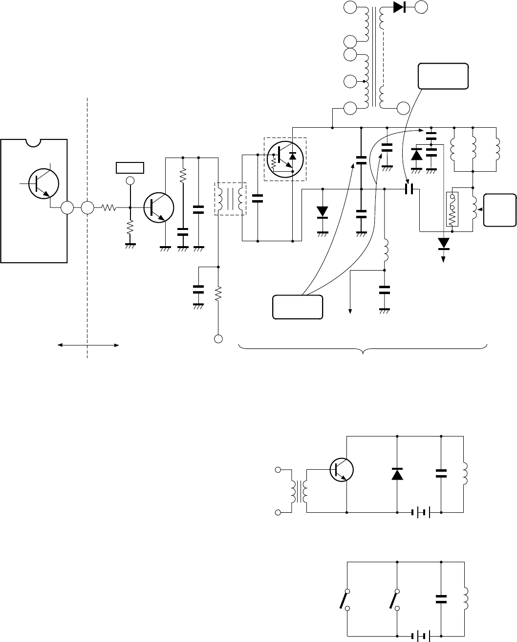
68
4. HORIZONTAL OUTPUT CIRCUIT
The horizontal output circuit applies a 15.625 kHz/15.734
kHz sawtooth wave current to the deflection coil with mu-
tual action of the horizontal output transistor and the damper
diode, and deflects the electron beam from left to right in
horizontal direction.
4-1. Theory of Operation
4-1-1. Operation of Basic Circuit
(1) To perform the horizontal scanning, a 15.625 kHz/
15.735 kHz sawtooth wave current must be flown into
the horizontal deflection coil. Theoretically speaking,
this operation can be made with the circuit shown in
Fig. 9-5 (a) and (b).
(2) As the switching operation of the circuit can be re-
placed with switching operation of a transistor and a
diode, the basic circuit of the horizontal output can be
expressed by the circuit shown in Fig. 9-5 (a). That is,
the transistor can be turned on or off by applying a
pulse across the base emitter. A forward switching cur-
rent flows for on-period, and a reverse switching cur-
rent flows through the diode for off-period. This switch-
ing is automatically carried out. The diode used for
this purpose is called a damper diode.
Fig. 9-5
(a) H output basic circuit
(b) H output equivalent circuit
H output
transistor DCo
L
Deflection
yoke
Resonant
capacitor
Damper
diode
Vcc
Vcc
SW1 SW2 Co L
Fig. 9-4
IC501
H. out
Q1 23 83
10
5
2
3
1
HV
8
S-charactor
capacitor
H
linearity
coil
Resonat
capacitor
Diode modulator circuit
To DPC output
SIGNAL DEF/POWER PCB
TP-33
BB81
R411
R410
C413
C416 R416
125V
Q402
H drive
R415
C417
T401
H drive
transformer
Q404
H output
(With damper diode)
T461
FBT
Deflection yoke
(H coil)
C463
D461
C444
C440
C423
C467
L441
R441
+
C464
+
L461
C343
D444
C418
D443
L462 L463 L464
To High Voltage
Regulator Circuit
69
Description of the basic circuit
1. t1~t2:
A positive pulse is applied to base of the output transistor
from the drive circuit, and a forward base current is flowing.
The output transistor is turned on in sufficient saturation area.
As a result, the collector voltage is almost equal to the ground
voltage and the deflection current increases from zero to a
value in proportionally. (The current reaches maximum at
t2, and a right half of picture is scanned up to this period.)
2. t2:
The base drive voltage rapidly changes to negative at t2 and
the base current becomes zero. The output transistor turns
off, collector current reduces to zero, and the deflection cur-
rent stops to increase.
3. t2~t3:
The drive voltage turns off at t2, but the deflection current
can not reduce to zero immediately because of inherent na-
ture of the coil and continues to flow, gradually decreasing
by charging the resonant capacitor C0. At the same time, the
capacitor voltage or the collector voltage is gradually in-
creases, and reaches maximum voltage when the deflection
current reaches zero at t3. Under this condition, all electro-
magnetic energy in the deflection coil at t2 is transferred to
the resonant capacitor in a form of electrostatic energy.
4. t3~t4:
Since the charged energy in the resonant capacitor discharges
through the deflection coil, the deflection current increases
in reverse direction, and voltage at the capacitor gradually
reduces. That is, the electrostatic energy in the resonant ca-
pacitor is converted into a electromagnetic energy in this
process.
5. t4:
When the discharge is completed, the voltage reduces to zero,
and the deflection current reaches maximum value in re-
verse direction. The t2~t4 is the horizontal flyback period,
and the electron beam is returned from right end to the left
end on the screen by the deflection current stated above.
The operation for this period is equivalent to a half cycle of
the resonant phenomenon with L and C0, and the flyback
period is determined by L and C0.
6. t4~t6:
For this period. C0 is charged with the deflection current
having opposite polarity to that of the deflection current
stated in "3.", and when the resonant capacitor voltage ex-
ceeds VCC, the damper diode D conducts. The deflection
current decreases along to an exponential function (approxi-
mately linear) curve and reaches zero at t6. Here, operation
returns to the state described under "1.", and the one period
of the horizontal scanning completes. For this period a left
half of the screen is scanned.
In this way, in the horizontal deflection scanning, a current
flowing through the damper diode scans the left half of the
screen; the current developed by the horizontal output tran-
sistor scans the right half of the screen; and for the flyback
period, both the damper diode and the output transistor are
cut off and the oscillation current of the circuit is used. Us-
ing the oscillation current improves efficiency of the circuit.
That is, about a half of deflection current (one fourth in terms
of power) is sufficient for the horizontal output transistor.
Fig. 9-6
A
B
C
D
E
F
G
H
t1 t2 t3 t4 t5 t6
0
0
0
0
0
0
0
0
TR
base voltage
TR
base current
TR
collector
current
D
damper
current (SW2)
Switch
current
(TR, SW1)
Resonant
capacitor
current (Co)
Deflection
current (Lo)
TR
collector
voltage
70
Amplitude Correction
To vary horizontal amplitude, it is necessary to vary a
sawtooth wave current flowing into the deflection coil. These
are two methods to vary the current; a method which varies
LH by connecting a variable inductance L in series with the
deflection yoke, and a method which varies power supply
voltage (across S-character capacitor) for the deflection yoke.
As the DPC circuits is used in the this chassis, the later
method which varies the deflection yoke power supply volt-
age by modifying the bus data is used.
4-1-2. Linearity Correction (LIN)
(1) S-curve Correction (S Capacitor)
Pictures are expanded at left and right ends of the screen
even if a sawtooth current with good linearity flows in
the deflection coil when deflection angle of a picture
tube increases. This is because projected image sizes
on the screen are different at screen center area and
the circumference area as shown in Fig. 9-7. To sup-
press this expansion at the screen circumference, it is
necessary to set the deflection angle q1 to a large value
(rapidly deflecting the electron beam) at the screen
center area, and to set the deflection angle q2 to a small
value (scanning the electron beam slowly) at the cir-
cumference area as shown in Fig. 9-7.
In the horizontal output circuit shown in Fig. 9-8, ca-
pacitor CS connected in series with the deflection coil
LH is to block DC current. By properly selecting the
value of CS and by generating a parabolic voltage de-
veloped by integrating the deflection coild current
across the S capacitor, and by varying the deflection
yoke voltage with the voltage, the scanning speed is
decreased at beginning and end of the scanning, and
increased at center area of the screen. The S curve cor-
rection is carried out in this way, thereby obtaining
pictures with good linearity.
Fig. 9-7
Fig. 9-8
θ
2
θ
1
t2 t1
t2 = t1
θ
2
θ
1
<
θ
2
θ
1
t2 t1
t2 > t1
θ
2
θ
1
=
(a) S-character correction (b)
TR D Co
Cs
L
H
Deflection coil
(a) H output circuit
(b) Sawtooth wave current
(c) Voltage across LH
Fast deflection
Slow deflection
(d) Synthesized current
Vcc
71
(2) Left-right Asymmetrical Correction (LIN coil)
In the circuit shown in Fig. 9-9 (a), the deflection coil
current iH does not flow straight as shown by a dotted
line in the Fig. 9-9 (b) if the linearity coil does not
exist, by flows as shown by the solid line because of
effect of the diode for a first scanning (screen left side)
and effect of resistance of the deflection coil for later
half period of scanning (screen right side). That is, the
deflection current becomes a sawtooth current with bad
linearity, resulting in reproducing of asymmetrical pic-
tures at left and right sides of the screen (left side ex-
panded, right side compressed).
When a horizontal linearity coil L1 with a current char-
acteristic as shown in Fig. 9-9 (c) is used, left side pic-
ture will be compressed and right side picture will be
expanded because the inductance is high at the left side
on the screen and low at the right side. The left-right
asymmetrical correction is carried out in this way, and
pictures with good linearity in total are obtained.
Fig. 9-10
Fig. 9-9 Linearity coil
(a)
(b) Deflection coil current
Deflection coil current
(iH)
0Characteristic of D
Resistance of LH
(c) Linearity coil characteristic
Linearity coil characteristic
Inductance
(µH)
(Left) (Right)
(Left) (Right)
Current (A)
TR D Co LH
Deflection
coil
FBT
Vcc
iH Li
Cs
S-character
capacitor
TR D Co
LH
LI
L
C
Cs
(b) Sawtooth wave current
(a)
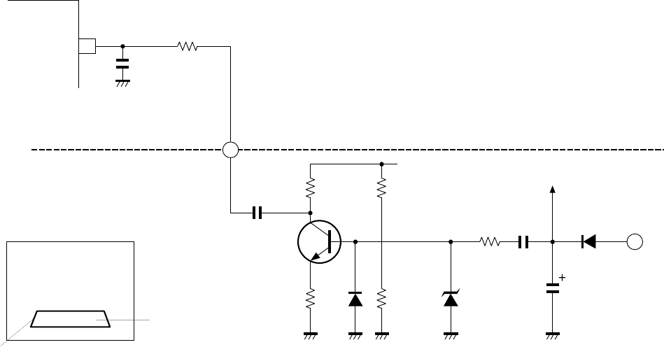
72
4-2. White Peak Bending Correction Circuit
4-2-1. Outline
White peak area in screen picture may sometimes cause bend-
ing in picture. See figure below.
In TP48E60 series, correction signal which video ripple in
video output circuit power supply 200V is input to pin 24
(Bending correction terminal) of Q501. This corrects white
peak bending.
4-2-2. Operation Theory
Fig. 9-11 shows circuit diagram. Video ripple in video out-
put circuit power supply 200V suffers DC cut by C475, and
is inverted in Q470, then input to pin 24 of Q501 via C481.
Pin 24 of Q501 is a bending correction terminal. The volt-
age which is applied to this terminal, controls phase of video
signal to correct white peak bending.
Q501
24
Bending correction
terminal
EHT
C415
93
Receiving Board
Power, Def board
BB91
C481 Inversion
Q470
R481
R482
D470
R483
R484 D474
R478
C475
C466
D406
200V
9V
White peak
Bending by white peak
T416
3
R379
Fig. 9-11 White peak bending correction circuit
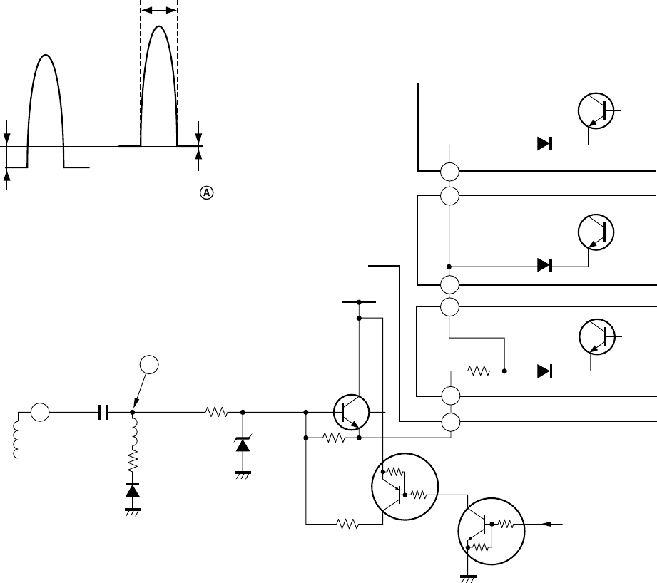
73
4-3. H Blanking
4-3-1. Outline
The H blanking circuit applies a blanking precisely for the
horizontal flyback period so that undesirable pictures fold-
ing does not appear at screen ends.
This unit allows the users to adjust an horizontal amplitude
adjustment, so, picture quality at screen ends will be im-
proved. This is one of the purposes of the blanking circuit.
4-3-2. Theory of Operation
The H blanking circuit determines the flyback period pre-
cisely from the AFC pulse in the FBT and applies the period
to emitter of the video output stage transistor on the CRT-D
PC board.
4-3-3. Circuit Operation
As can be seen from Fig. 9-12, the flyback period of the
AFC pulse in the FBT starts at a negative side from 0V. To
detects this, the DC component is cut with C493. This is,
C493 is always charged through D487 with a negative side
(about –17V) of the AFC pulse. As a result, a voltage at point
A in the waveform rises from the ground level. This wave-
form is sliced in a circuit (R486, D486) to detect the flyback
period. Thus obtained voltage is applied to Q901, Q911, and
Q921 through D904, D914, D927 and cuts off them thereby
blanking the resters.
0V
Approx.
-17V AFC Pulse
Q487
ON period
D486
Slice level
Waveform at
point
Fig. 9-12
T461 (FBT)
AFC
10
A
Point
C493
D487
R409
R486
D486 R417
R438
V blanking
Q488
Q489
P903
P904
R906
+35V
Q487
D914
D904
Q901
Q911
CRT-D DCB
Deflection/Power PCB
7
6
10
10
D927
Q921
BLUE
CRT/D
GREEN
CRT/D
RED
CRT/D
10
10
L410
Fig. 9-13
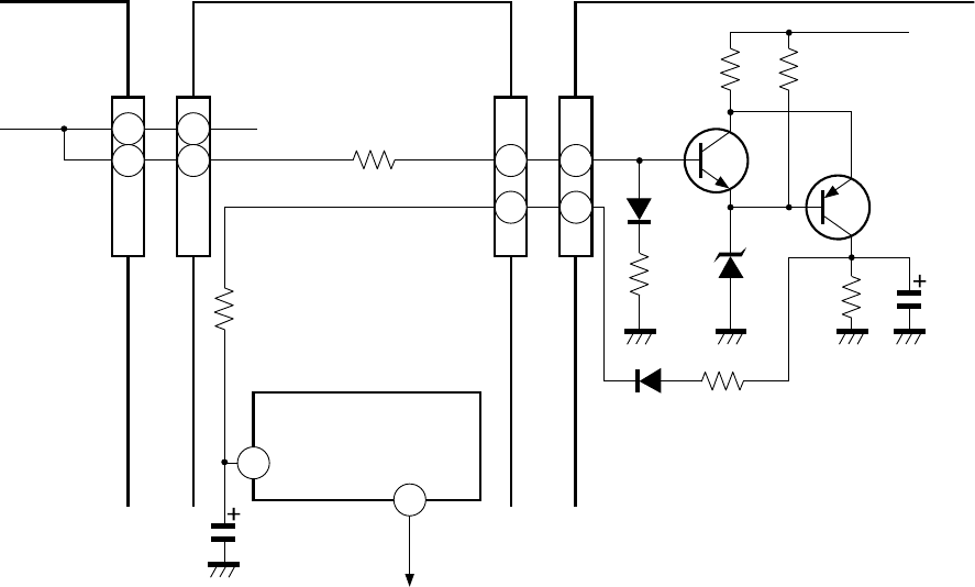
74
4-4. 200V Low Voltage Protection
4-4-1. Outline
When the video output power supply 200V is stopped by
some abnormality occurence, the current inside CPT in-
creases abnormally. So the CPT may be damaged. To pre-
vents this, a 200V low voltage protection circuit is provided.
4-4-2. Theory of Operation
Fig. 9-14 shows a connection diagram.
Under a normal condition Q340 is always on because of about
210V supplied from the 200V line. Accordingly Q340 col-
lector is kept at about 6.2V or the zener voltage of D341 and
Q341 is turned off.
If some abnormality occurs and 200V line voltage lowers
by less than about 160V. Q340 turns off and its collector
voltage rises. So Q341 turns on. With Q341 turned on the
voltage at pin 14 of Z801 (expander) exceeds a threshold
voltage and pin 16 of Z80 is high level and makes the power
relay turn off.
CRT-D Circuit Deflection circuit
200V 11
22
P405
R436
P301
Z801
14
16
GATE PROTECTOR
8
17
8
17
DPC circuit
P350 R389 R390
-12V
Q340
Q341
D340
R391
D341 R392 C340
R346
R879
C894
D315
Fig. 9-14
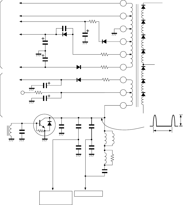
75
5. HIGH VOLTAGE GENERATION CIRCUIT
Fig. 9-15
The high voltage generation circuit develops an anode volt-
age for the picture tube, focus, screen, CRT heater, video
output (210V) and so on by stepping up the pulse voltage
developed for flyback period of the horizontal output cir-
cuit with the FBT, and supplies the power to various cir-
cuit.
5-1. Theory of Operation
10
9
4
7
6
3
2
1
5
Auxiliary
winding
Primary
winding
AFC
blanking
Heater
+35V
-27.5V
+210V
+125V
C310
C303
D302
C460 D460
R327
R469
D406
C446
C448
Q404
C463
T401
CRT
anode
ABL
H deflection coil
L462/L463/L464
R441
C423
L441
1040V
(p-p)
1H
(15.625kHz)
R444
R443
Focus pack
D408
C447
R448
+12V-1
DPC CIRCUITHIGH VOLTAGE
REGULATOR
CIRCUIT
C440 C444
C467
C443
C418
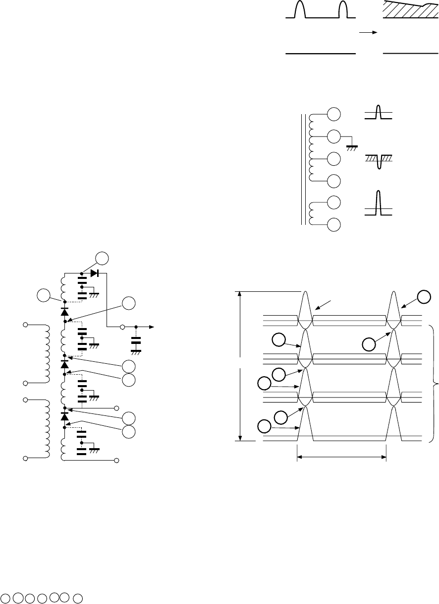
76
5-1-1. +210V
For the flyback period, pulses are stacked up to DC +125V
with FBT, and the voltage is rectified by D406 and filtered
by C446.
5-1-2. +35V, 12V
Pin 4 of the FBT is grounded and the shaded area of nega-
tive pulse developed for opposite period of the flyback pe-
riod is rectified, thus developing better regulation power
supply.
5-1-3. –27V
As a power for the DPC circuit, a negative pulse signal is
rectified by D460 and filtered with C460, thus developing
the –27V.
5-1-4. High Voltage
Singular rectification system which uses a harmonics non-
resonant type FBT is employed and a better high voltage
regulation is obtained, so amplitude variation of pictures
becomes low.
Fig. 9-16
Fig. 9-17
+125V
0
10
4
7
6
2
1
0
0
0
For +12V
+35V
G
FE
D
C
B
A
E
D
C
B
A
G
F
Primary
Auxiliary
Picture
tube anode
EO
ABL
EH
Pulse
Stacked
pulse of
4 block
1H
15.735KHz
Picture
tube capacitor
Fig. 9-18
5-2. Operation Theory of the Harmonic Non-Resonant System and Tuned Waveforms
The high voltage coil is of film multi-layer winding type
and the coils are isolated into seven blocks. Each block is
connected through a diode.
The basic operation is described in the case of 4 blocks con-
struction for simplification. Positive or negative pulse deter-
mined by stray capacitance of each coil develops at terminal
points ( A , B , C , D , E , F , G ) of each coil as shown in Fig. 9-
18, and these pulses are stacked as shown, thus developing
the high voltage.
Moreover, a capacitance between the internal and external
coatings of the picture tube works as a smoothing capacitor.
Focus voltage is obtained at point EO.
77
6. HIGH VOLTAGE CIRCUIT
6-1. High Voltage Regulator
6-1-1. Outline
Generally, four kinds of methods exist to stabilize a high
voltage in high voltage output circuits using the FBT:
(1) Stabilization by varying the power supply voltage.
(2) Stabilization by varying L value with a saturable reac-
tance connected in series with the primary winding of
the FBT.
(3) Stabilization by varying equivalent capacitance of the
resonant capacitor C0.
(4) Stabilization by superimposing a DC or pulse (this
varies the high voltage) on a lower voltage side of the
high voltage winding of the FBT.
In this unit, pulse transformer is eliminated and the regula-
tor circuit using the method (3) is employed. The block dia-
gram is shown in Fig. 9-19.
The VCP2 developed across C2 is DC-clamped with a diode
D1 and the resultant voltage is smoothed with a diode D2
and a capacitor C3. Thus processed voltage is obtained at
the point B . This voltage is used to provide a base current
for the transistor Q1 or to flow the collector current. The
voltage at the point B decreases with the circuit impedance
and finally lowers up to a VCE saturation voltage of Q1.
Then, VCP2 is not clamped by D2 with the voltage at the
point B . Since the VCP is expressed as a sum of VCP1 and
VCP2 as shown by equation 3 , VCP decreases by amount
the VCP2 is decreased. This varies the high voltage.
Q1 collector current is controlled by Q1 base current which
is an output of the comparison inverted amplifier. That is,
the Q1 base current is controlled by a voltage obtained by
comparing a detection voltage of the top breeder of the FBT
(9.1V) and a DC voltage of 9V.
VCP1 = VCP 1
VCP2 = VCP 2
VCP = VCP2 3
C1 + C2
C2
C1 + C2
C2
C1 + C2
C2
Fig. 9-21
Hotizonal
output D
Y
T461
FBT
ANODE
125V
PW output
-27V
High voltage Reg.
V.
Ref.
Z450
CR-BLOCK
Fig. 9-19 Basic circuit for high voltage regulator
emplyed in the unit
6-1-2. Theory of Operation
Fig. 9-20 shows a basic circuit of the high voltage regulator
used in the unit.
The high voltage regulator circuit splits a resonant capacitor
C0 to C1 and C2. thereby dividing the collector voltage (VCP)
of the H output transistor with C1 and C2.
Here, assume each voltage developed across C1 and C2 as
VCP1 and VCP1, respectively,
each relation can be expressed by the above equations
1 ~ 3 .
Horizontal
output C1 L
H
FBT
L
P
B
D1
C2
C3
D2
Q1 High voltag
e
Reg.
output amp
CS +B
Fig. 9-20
V
CP
= V
CP1
+ V
CP2
V
CP
1
V
CP
2
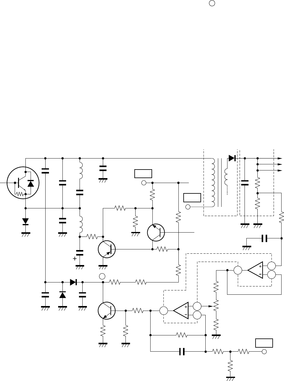
78
6-1-3. Actual
Fig. 9-22 shows the actual circuit used in the unit.
A resonant capacitor C0 is also split into two capacitors C443
and C444 in this circuit. The high voltage regulator cirucits
is structured by splitting the C443 to two capacitors of C443
and C448.
Here, assume a high voltage increases and the detection volt-
age ED' obtained by dividing the high voltage also increases
in proportional to the high voltage. This makes the voltage
ED increase at pin 7. (The voltage is impedance transformed
by a voltage follower circuit consisting of op amplifier Q483
at pin 7.)
The voltage ED and a 9V reference voltage developed by a
3-terminal regulator Q420 are compared. When the ED in-
creases, the voltage at pin 2 of Q483 differential amplifier
also increases, and the base current IB of the high voltage
transistor Q480 increases.
As a result, Q480 collector current increases and Q480 col-
lector voltage (at the point B ) decreases. Then, a peak value
of VCP2 across C418 is clamped by the diode D443 at the
collector voltage lowered, and the collector voltage VCP of
Q404 (H output transistor) obtained as a sum of the voltage
VCP1 across C443 and VCP2 across L418 decreases. Then,
the high voltage also decreases.
When the high voltage lowers, the corrective operation is
carried out in reverse order.
* Resustors R451, R452, R453 and R455 are used to cor-
rect undersirable influence (H amplitude increase at mini-
mum IH) by the H amplidude regulator.
Fig. 9-22 Actual high voltage regulator circuit
Horizontal
output Q404 C443
C444 C
S
L462
L463
L464
D461
C467
L461
R463
C440 -27V
C464
Q460
R466
R461/R469
R460
Q462 R455
125V
R454
R453
R452
R451
B
D443
C418
D444
C419 Q480 R434
R431 R492
23
4
R488
C483 R494 R439
R487
Q420
9V-1
86
7
E
D
Q483 C482
R435
E
D
'
FBT E
H
R489
R450
R490
CR-BLOCK
79
Then Q463 turns on. By this Tr6 and Tr6 turn on to make
ON/OFF pulse at pin 7of QA01 in low level, Q846 and Q845
turns off, then relay SR81 turns off. Tr6 and Tr7 are in thy-
ristor-connection, and 5V of power holds protection opera-
tion until main power switch is turned off. During circuit
operation, power LED near main power switch blinks turn
on and off in red.
Caution:
• To restart TV set, repair failure first.
7. X-RAY PROTECTION CIRCUIT
7-1. Outline
In case picture tube using high voltage, when high voltage
rises abnormally due to components failure and circuit mal-
function, there is possible danger that X-RAY leakage in-
creases to affect human body. To prevent it, X-RAY protec-
tion circuit is equipped.
7-2. Operation
Figure 9-23 shows the circuit diagram. Supposing high volt-
age rises abnormally due to some reason, pulse at pin 9 of
T461 also rises, and detection voltage ED rectified by D471
and C471 in X-RAY protection circuit rises. When ED rises,
emitter voltage of Q464 divided by R459 and R462 becomes
higher than [zener voltage (6.2V) of D458 + Q464 VBE ].
This causes Q464 turns on to supply base current to Q463.
Fig. 9-23 X-RAY protection circuit
R
ELAY
S
R80
Q846
Q845
Tr5
Tr6
Tr7
R11
R12
R9
R10
R19
C1
C894
R879
R467
12V
D459
R468
C458
R458
R462
R459
Q463 Q464
C471
R472
D471
9
T461
D458
14
17
16
Z801
C459
5V
E
D
15
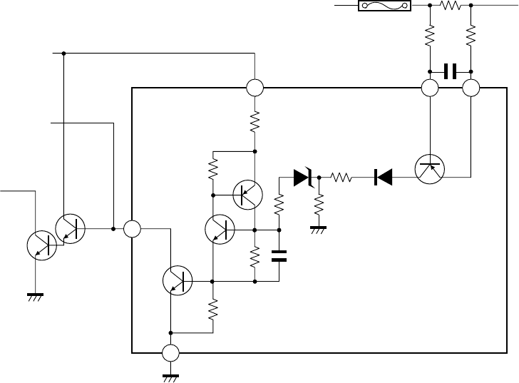
80
8. OVER CURRENT PROTECTION CIRCUIT
8-1. Outline
If main power (125V) current increases abnormally due to
components failure, there is possible danger of the second-
ary damage like failure getting involved in other part fail-
ure, and abnormal heating. To prevent this, over current pro-
tection circuit is equipped, which detects current of main B
line to turn off power relay in abnormal situation.
8-2. Operation
Fig. 9-24 shows over current protection circuit. When the
current of main B line increases abnormally due to the
shortage in load of main B line, voltage drop arises across
R470. By this voltage drop, when base-emitter voltage of Tr8
in protector module (Z801) becomes approx. 0.7V or more,
Tr8 turns on, and the voltage by divided ratio of R15 and R16
is applied to cathode of ZD4. When this voltage becomes
higher than zener voltage of ZD4, ZD4 turns on to supply base
current to base of Tr6 via R14. This causes Tr5 ON and
voltage at pin 16 of Z801 becomes low.
Therefore, QB30 and Q843 turns off to set SR81 OFF. Tr6
and Tr7 in Z801 are in thyristor-connection, and power 5V-
1 supplied at pin 15 keeps protection operation for standby
power until main power switch is turned off. During circuit
operation, power LED near main power switch blinks in red.
Caution:
• To restart TV set, repair failure first.
Fig. 9-24 Over current protection circuit
16
15
17
21
5V
MICON
QA01#7
RELAY
SR80
Q845 Q846
MAIN B
R470
F470
To T461
R479
R471
C472
R16
R15
R14
R12
R11
R9
R10
ZD4
C1
Tr6
Tr5
Tr7
Tr8
D1
Z801
PROTECTOR MODULE
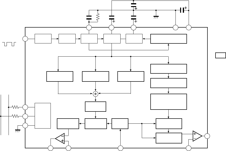
81
(4) V picture position (neutral voltage setting)
(5) V M-character correction
(6) V EHT correction
(7) H amplitude
(8) L and R pin-cushion distortion correction I (entire area)
– Not used for this model.
(9) L and R pin-cushion distortion correction II (corner
portions at top and bottom) – Not used for this model.
(10) H trapezoid distortion correction – Not used for this
model.
(11) H EHT correction
(12) V AGC time constant switching
1-3. Block Diagram
Fig. 10-1 shows a block diagram of the basic circuit.
1. DEFLECTION DISTORTION CORRECTION IC (TA8859CP)
1-1. Outline
The deflection distortion correction IC (TA8859CP), in com-
bination with a V/C/D IC (TA1222AN) which has a V pulse
output, performs correction for various deflection distortions
and V output through the I2C bus control. All the I2C bus
controls are carried out by a microcomputer and can be con-
trolled with the remote control.
1-2. Functions and Features
The IC has functions of V RAMP voltage generation, V
amplitude automatic switching (50/60 Hz), V linearity cor-
rection, V amplification, EHT correction, side pincushion
correction, I2C bus interface, etc. and controls following
items through the I2C bus lines.
(1) V amplitude
(2) V linearity
(3) V S-character correction
V. Trigger-in
(Bus Control Signal)
SDA SCL
10
9
12
13
14 15 16 5 3
2
4
168
+9V
control through
bus
EW-drive
V drive V. feedback EHT INPUT EW feedback
Waveform
shape
Trigger
det
Puise
Gen. V. Rame A G C V. AGC time
constant SW
H. trapezoid distortion
correction
L-R pincushion
distortion correction I
L-R pincushion
distortion correction II
(Top & bottom comer section)
H.EHT
correction
H. Amplitude
Adj.
H.EHT
input
V. EHT
correction
V. screen
position
V. Amplitude
Adj.
V. M-Character
correction
V. linearity
correction
V. S-character
correction
Logic
Fig. 10-1
SECTION X: DEFLECTION DISTORTION CORRECTION CIRCUIT
(SIDE DPC CIRCUIT)
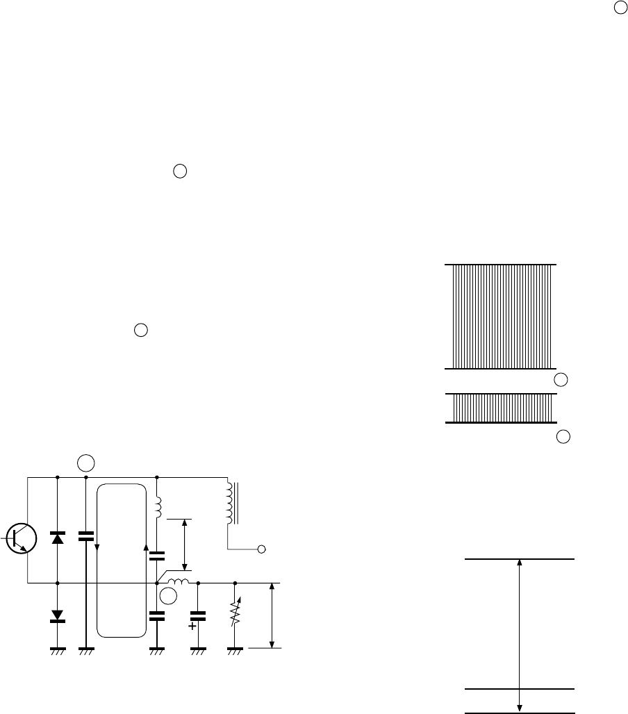
82
When the negative pulse developed at the point B is inte-
grated with Lm and Csm, its average value appears at Csm
as a negative voltage.
By modulating this voltage with Q460, a waveform of Vm is
obtained as shown in Fig. 10-3 b). As a result, the voltage
VS which is the sum of the power supply voltage VB and the
Vm is applied across the S-curve capacitor CS. The VS be-
comes as a power source for the deflection yoke as shown in
Fig. 10-4, is applied to the horizontal deflection yoke.
2. DIODE MODULATOR CIRCUIT
In N5SS, the distortion correction is carried out by the ditigal
convergence circuit. So the component of the diode modu-
lator circuit is the same as that of conventional television,
because it is used only for the horizontal oscillation adjust-
ment.
Fig. 10-2 shows a basic circuit of the diode modulator used
in the N5SS.
A key point in the modulation circuit shown in Fig. 10-2 is
to develop a negative pulse at point B .
In this circuit, a current loop of the resonant circuit for flyback
period is shown by an arrow, and the energy stored in LDY is
transferred to resonant capacitors Cr, Crm in passing through
Cr, Crm, CS when the scanning completes. As a result, a
positive, horizontal pulse as shown in Fig.
10-3 a) will appear at Cr, and the current flows into Crm
with the direction as shown. Then a pulse as shown in Fig.
10-3 b) develops at the point B.
On the other hand, since constant amplitude pulses across
Cr, as shown in Fig. 10-3, are applied to the primary wind-
ing, the high voltage of FBT also develops a constant volt-
age.
A
B
H
OUT
DD Cr
DM
L
DY
FBT
V
B
Cs Vs
Crm Csm
Q460 Vm
Lm
Fig. 10-2
a) Waveform at point A
b) Waveform at point B
0
0
Fig. 10-3
Fig. 10-4
VS
V
B
0
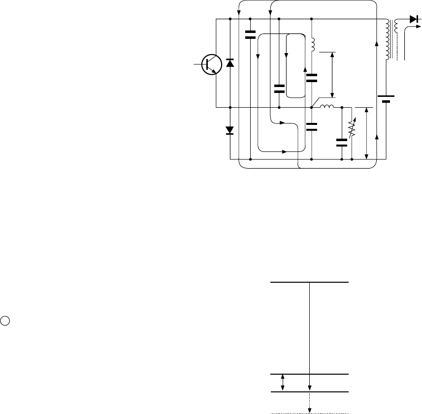
83
3. ACTUAL CIRCUIT
In the actual circuit, the resonant capacitor is split into two
as shown in Fig. 10-7. One, C440, is inserted between the
collector of the H. OUT transistor and ground and another
C444 inserted between the collector and emitter. In Fig. 10-
5, C440 is expressed as C1 and C444 as C2, and the resonant
current path for the flyback period is shown by arrows.
In a conventional circuit, when brightness of a picture tube
varies, high voltage current varies and the high voltage also
varies. As a result, horizontal amplitude also varies.
However, in this circuit, the horizontal amplitude variation
can be suppressed to near zero if the high voltage current
varies with variation of the high voltage.
When the scanning period completes, the energy stored in
the deflection yoke LDY is transferred to the resonant ca-
pacitor in a form of current IY. In this case, the current is
split into two; IY1 passing through C1, C3 and IY2 passing
through C2. In the same way, the energy stored in the pri-
mary winding of the FBT is transferred to the resonant ca-
pacitor in the form of IP. In this case, the current (path) is
also split into two; IP1 passing through C1 and IP2 passing
through C2, C3. Concequently, the current differences be-
tween IY1 and IP2 (IY1-IP2) passes through C3.
When the high voltage current IH reduces with a dark pic-
ture, the current IP in the primary circuit decreases, so IP1
and IP2 also decrease. However, a current flowing into (IY1-
IP2) increases as IP2 decreases. As a result, the pulse devel-
oping at the point B increases and the voltage Vm at Csm
also increases as shown in Fig. 10-8. That is, when a dark
picture appears, the voltage across S-curve capacitor CS in-
creases as shown in Fig. 10-8, the high voltage rises, and the
horizontal amplitude is going to decrease. But, as VS in-
creases, the deflection yoke current increases and this works
to increase the horizontal amplitude. Accordingly, if the
brightness of picture changes, the horizontal amplitude is
maintained at a constant value. This is one of the fine fea-
tures the circuit has.
FBT
I
H
V
B
Vm
Csm
C
3
V
S
C
S
Lm
C
2
I
P2
I
Y1
I
Y1
C
1
I
Y
I
P2
I
P1
L
DY
H.
OUT
I
P
I
Y2
VS
V
B
0
Vm
Fig. 10-5
Fig. 10-6
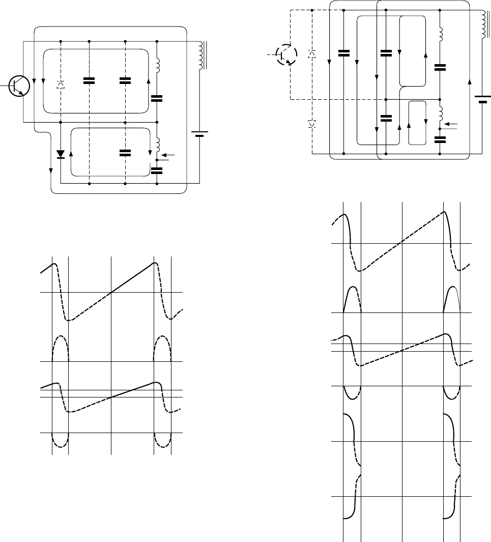
84
3-1. Basic Operation and Current Path
3-1-1. Later Half Scanning Period
When the power is turned on, the power supply voltage VB
is applied to CS and Csm, and the CS acts as a power source
for a later half of the scanning period for which the H. OUT
transistor is turned on, and the deflection current IY flows in
the path as shown below.
3-1-2. First Half Scanning Period
When the base drive current decreases and the H. OUT tran-
sistor is turned off, each energy stored in LDY, Lm, LP of
FTB is transferred to C1, C2 and C3, respectively, and the
resonant current becomes zero at a center of the flyback pe-
riod. Then, VA and VB pulses show a maximum amplitude.
H.OUT
V
A
FBT
L
DY
lP
Cs
V
B
V
B
D
M
I
M
L
M
I
DC
C
SM
+
I
Y
+
V
A
FBT
L
DY
lP
Cs
V
B
V
B
I
M
L
M
I
DC
C
SM
I
Y
I
Y2
I
P2
C
2
C
1
I
P1
Fig. 10-7
Fig. 10-8
Fig. 10-9
Fig. 10-10
I
Y
V
A
0
0
0
0
I
DC
I
M
V
B
0
C
1
C
2
0
C
3
C
1
: I
Y1
+I
P1
C
2
: I
Y2
+I
P2
C
3
: I
P2
-
I
Y1
-
I
M
Voltage & current waveform in H period.
I
Y
V
A
0
0
0
0
I
DC
I
M
V
B
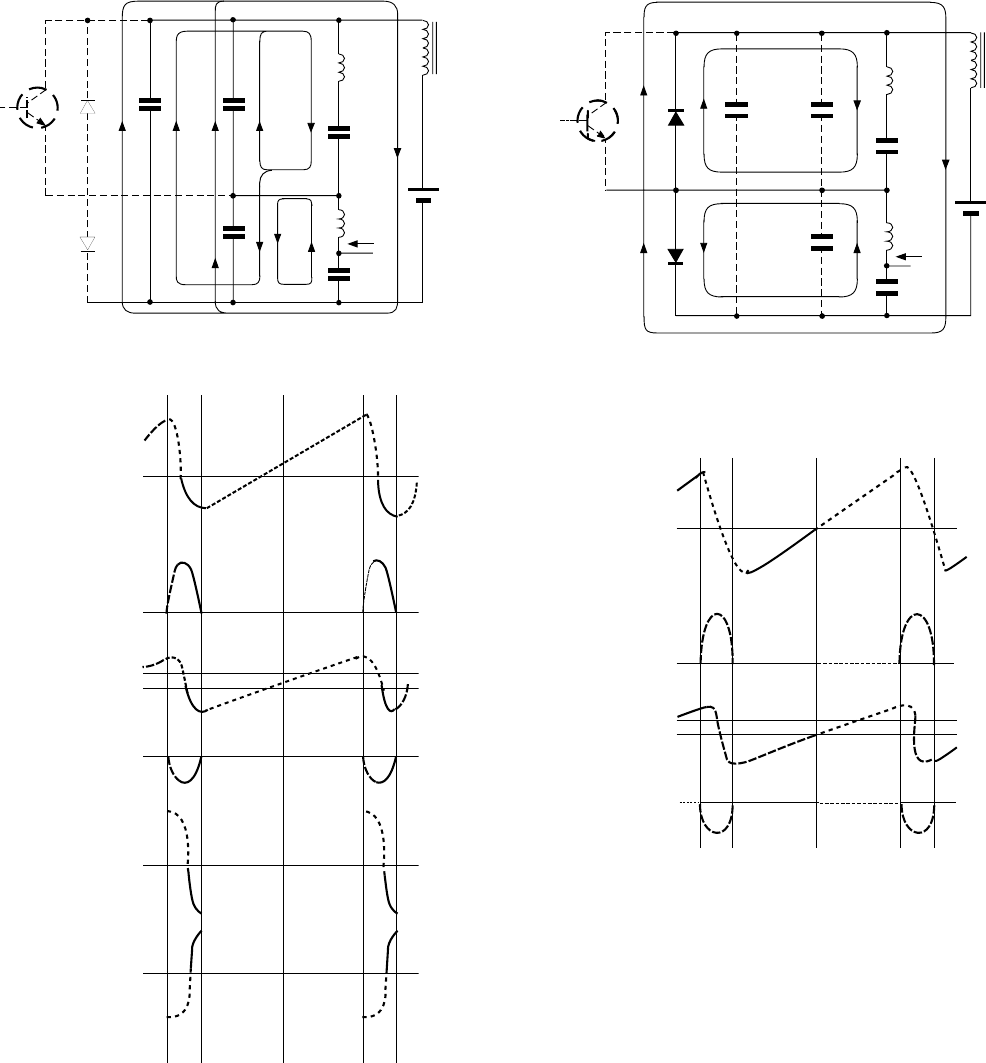
85
3-1-3. Later Half of Flyback Period
All energy in the coil has been transferred to the resonant
capacitors at the center of the flyback period, and the volt-
age shows the maximum value. However, during next half
of the flyback period, the energy of the resonat capacitor is
discharged as a reverse current through respective coil. When
the discharge has been completed, VA and VB becomes zero,
and the deflection current in reverse direction becomes the
maximum.
3-1-4. First Half of Scanning Period
When the flyback period completes, the damper diode DD
and the modulation diode DM turn on, and the IY and IM
proportionally decrease from the maximum value to zero.
The H. OUT transistor is turned on just preceding at the center
of the scanning period, and repeats the steps 3-1-1 through
3-1-4 stated above.
I
P1
I
P2
C
1
C
2
V
A
L.O.P.T
I
Y
I
Y2
L
DY
I
P
C
S
V
B
V
B
L
M
I
DC
C
3
I
M
C
SM
I
Y1
D
D
V
A
FBT
I
Y
L
DY
C
S
V
B
V
B
L
M
I
M
C
SM
I
M
D
M
Fig. 10-11
Fig. 10-12
Fig. 10-13
Fig. 10-14
Iy
V
A
0
0
0
0
I
DC
I
M
V
B
0
C
1
C
2
0
C
3
C
1
: I
Y1
+I
P1
C
2
: I
Y2
+I
P2
C
3
: I
P2
-
I
y1
-
I
M.
Voltage & current waveform in H period.
I
Y
V
A
0
0
0
0
I
DC
I
M
V
B
86
1. OUTLINE
The digital convergence circuit develops outputs to correct
screen distortion and perform color matching. The digital
convergence circuit used is of an all digital type and allows
good adjustments in comprise with a conventional analog type
circuit.
Followings are features of the digital convergence circuit.
1) No adjustment controls (volumes)
2) Registration accuracy increased.
3) Space saved
4) Adjustment by a remote control
The data adjusted are classed into 4 screens for each screen
mode. These data are stored on E2PROMs inside the unit.
The memory size used in this case is 4 Kbits per one screen.
Each screen adjustment is carried out by calling the adjust-
ment screen with the remote control unit supplied and the
adjustment is carried out according to the dimensions speci-
fied for each screen. The control of the unit is carried out in
the I2C format.
2. CIRCUIT DESCRIPTION
2-1. Configuration
Fig. 11-1 shows a block diagram. The digital convergence
unit consists of Q701 T7K64 which plays a major role, Q707
PLL circuit which locks a sync entered, Q713 E2PROM to
store the data, and Q703-5 D/A converter which develops a
correction wave form.
The output signal from the Q703 – 705 D/A converter is
amplified and wave form shaped by Q715, Q717 and Q719,
and comes out from the unit.
The clock signal for the PLL is adjusted by L719 to a refer-
ence frequency of 32 ± 0.1MHz under no input status.
A test pattern generator is also built inside Q701 and devel-
ops R, G, B signals and a Ys switching signal.
2-2. Circuit Description
(1) With the power turned on, the unit is reset and enters
an operation standby status. And a sync signal of the
unit enters external Q707 and Q701. The signal en-
tered Q707 is counted down by a counter inside the
Q701 and this is used as the reference clock. Q701
works in synchronization with the reference clock sig-
nal and the sync signal.
(2) A command is sent from the microcomputer in the unit
and Q701 is set up to load the data in Q713 to the in-
ternal RAM. (8 (horizontal) x 7 (vertical) x 3 (color))
(3) Q701 transfers a serial data specified to Q703 – 705
according to the RAM data. In this case, interpolation
for the RAM data is automatically carried out by a built
-in digital filter inside Q701.
(4) The serial data sent from Q701 are digital-analog con-
verted by Q703 – 705, thus developing the analog type
wave form.
(5) The signals sent from Q703 – 705 are amplified Q715,
Q717, Q719, respectively, and then filtered in the next
stage to smooth and shape the wave form. Thus pro-
cessed signals are used as H and V correction wave
forms for R, G, and B signals.
SECTION XI: DIGITAL CONVERGENCE CIRCUIT
87
Fig. 11-1 Block diagram
Filter
Filter
Filter
Filter
Filter
Filter
D/A
D/A
D/A
R
G
B
Ys
RAM (8
∗
8
∗
12bit)
∗
3
Q715
Q717
Q719
Q705
Q704
Q703
GH
GV
BH
BV
RV
RH
Counter
PLL
HD
VD
Q707
Q719 32MHz
Q767
M-CON
DATA
CLK
RESET
R716, C711
E
2
PROM
MEMORY
Q701 T7K64
Load
Save
Q713
Main bus line
Test pattern
88
3. PICTURE ADJUSTMENT
Four screens for Normal/Full, Theater wide 1, Theater Wide
2, Theater Wide 3 are provided for the adjustments. When
making the adjustments, receive the U/VHF or CABLE
broadcasting signal or the built-in pattern signal of the mi-
croprocessor to make a synchronization with the frequency
of the adjusting screen with the unit..
This adjustment program is prepared as the microprocessor
function of the set and it is possible to adjust by the remote
controller attached.
3-1. Outline of the Modification Process of
the Storing Adjustment Data
Set the convergence adjustment screen.
The adjusted data is stored in the memory inside Q713
E2CPROM which is a non-volatile memory.
The RAM data inside Q701 is lost when the power turns
off. So the initial operation status is set by the software com-
mand from the microprocessor QA01 every time when the
unit turns on.
The data adjusted manually through the screen by displaying
the adjusting screen on the display is once written on RAM
inside Q701. Adjust each adjusting point and store the modi-
fied total data on RAM as correct one into Q713 E2PROM.
The adjustment is carried out for each screen mode, and its
order is as follows; Normal/Full ® Theater Wide 1 ® the-
ater Wide 2 ® Theater Wide 3. (When the adjustment value
is saved after adjusting Normal/Full, the microprocessor cal-
culates the adjustment values for Theater Wide 1, 2 and 3
based on the adjustment value of Normal/Full mode and sets
the values for Theater Wide 1, 2 and 3 to the closed values to
require minimum adjustment.)
Normal full distortion
modification
(G screen)
Normal full
color matching
(R, B screen)
Theater wide 1
distortion modification
(G screen)
Theater wide 1
color matching
(R, B screen)
1. Push "7" key of the remote
controller to save.
2. turn "PIC-SIZE" key of the
remote controller ON
Theater wide 2
distortion modification
(G screen)
Theater wide 2
color matching
(R, B screen)
Theater wide 3
distortion modification
(G screen)
Theater wide 3
color matching
(R, B screen)
1. Push "7" key of the remote
controller to save.
2. turn "PIC-SIZE" key of the
remote controller ON
1. Push "7" key of the remote
controller to save.
2. turn "PIC-SIZE" key of the
remote controller ON
1. Push "7" key of the remote
controller to save.
2. turn "PIC-SIZE" key of the
remote controller ON
END
Fig. 11-2
89
3-2. Service Mode
3-2-1. Outline
The service mode, one of the functions this unit provides, is
controlled by the microprocessor QA01 and .
This mode is set by the special operation to avoid the easy
operation by the user. Move the cursor to between the adjust-
ment points of 8*7/each color and modify the data directly.
Before entering the service mode, perform the center adjust-
ment using the color unmatching adjustment in the user menu.
3-2-2. Entering/Exiting Mode
When the “MUTE” key on the remote controller is pressed,
the screen display appears. Pushing the “MUTE” key again
disappears the screen display.
In this status, when the “MENU” key on the set console is
pushed while pushing the “MUTE” key, S is displayed on
the upper right of the screen. When the “MENU” key is
pressed again, the service data is displayed on the upper left
on the screen.
When “7” key on the remote controller is pressed in this sta-
tus, the screen changes to display the cross hatch screen (the
first screen described later) and the convergence adjustment
screen appears.
When “7” key is pressed again, the data storing operation is
automatically carried out and the cross hatch + data display
screen (the second screen described later) appears.
When “7” key is pressed furthermore, the display returns to
the initial screen.
Service data display
(original picture)
Remote
"7" key
The first picture The second picture
Remote "7" key
+automatic save
Remote
"7" key
XX
++ MENU
Fig. 11-3
Note:
When changing the convergence correction data, always be
sure to perform the automatic storing operation. If the power
turns off without carrying out the automatic storing opera-
tion, the modified data is lost.
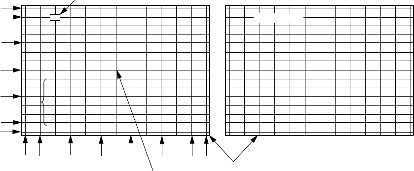
90
3-2-3. Initial screen
The screen mode is Normal/Full screen mode.
Correction point: Vertical 8 * Horizontal 7 (® and - marks
are the adjusting points.)
Fig. 11-4
(1) First screen:
The initial cross hatch screen appears. The pattern col-
ors are displayed with 3 colors. The cursor color is red
and left blinking.
When the modification is carried out, the last memory
status is displayed.
Cursor mode:
Lighting: Data modification mode
Blinking: Cursor move mode
The display color shows the color which can modify
the data.
(2) Second screen
When changing from the first screen to second screen, the
convergence correction waveform is mute for 1 second. The
modified data for this period is sent to Q713 E2PROM from
Q071 RAM and then stored.
The second screen is displayed upper left of the first screen,
so the convergence adjustment cannot be carried out when
the second screen is displayed.
Note:
• The adjusted data is automatically stored when the dis-
play changes from the first screen to the second screen.
So be sure to perform this operation after adjustment com-
pletes.
• Adjustment should be carried out with a corresponding
signal received.
12
3
45678
1
2
3
4
5
6
7
YCursor (Red) (Blinking)
Screen Center
X
X:3
Y:2
C:R
S:FULL
Adjusting point display
X : Horizontal position display
Y : Vertical position display
C : Color display
S : Screen mode display
Data display
Primary screen Secandary screen
Screen frame
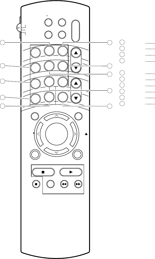
91
3-2-4. Key function of remote control unit
ADV/
POP CH
ADV/
PCB CH
23
56
89
4
7
¥
0
ENT
PIC SIZE
TV/VIDEO
RECALL
POWER
CH
VOL
CH RTN
EDS MENU
FAV FAV
EXITRESET
STOP SCURCE PLAY PCP
REC TV/VCR REW FF
CH SEARCH
STILL SWAP
MUTE
1
ENTER
TOSHIBA
100
TV
CABLE
VCR
1
2
3
4
7
9
4
5
3
6
8
10
1
2
100 Key
0 Key
ENT Key
5 Key
5
6
7
8
9
10
8 Key
2 Key
6 Key
4 Key
3 Key
7 Key
Red test pattern ON/OFF
Green test pattern ON/OFF
Blue test pattern ON/OFF
Cursor shift/data change
mode chang over
Cursor down/adjusting point down
Cursor UP/adjusting point UP
Cursor right/adjusting point right
Cursor left/adjusting point left
Cursor color change
Data save
Fig. 11-5
92
3-2-5. Operation procedure
(1) Set the screen to Normal or Full mode using the PIC-
SIZE key on the remote controller.
(2) Set the unit to the service mode with MUTE + MUTE
+ MENU keys pressed. (Entering to S mode.)
(3) Set the unit to the convergence adjusting mode by press-
ing the “7” key on the remote controller. (Fist screen)
(4) Select the pattern to display by pressing 100, 0, ENT
on the remote controller.
(Red adjustment; 100 ... ON, 0 ... ON, ENT... OFF)
(Green adjustment; 100 ... OFF, 0 ... ON, ENT... ON)
(Blue adjustment; 100 ... ON, 0 ... OFF, ENT... ON)
(5) Select the color to adjust by pressing “3” key on the
remote controller.
(6) Confirm that the cursor is in the movable status (the
cursor blinking status).
(7) Select the adjusting position by pressing “8”, “4” and
“6”.
3-3. Each Screen Adjustment Method
3-3-1. Normal/Full
B
2
B
2
14xB
2mm
12xA
40 inches 16:9 Screen size: Horizontal 885mm x Vertical 498mm
Dimension A: 73.5mm Dimension B: 33.2mm
Screen frame
2mm
Fig. 11-6
(8) When the adjusting position is determined, press “5”
key on the remote controller to enter the cursor blink-
ing status.
(9) Set the cursor to the adjusting position by pressing “2”,
“8”, “4” and “6”, and perform the pattern distortion
correction and color matching adjustments.
(10) Press “5” key again and move the cursor. Perform the
adjustment in the same way as described above.
(11) After the adjustment completes, perform the automatic
storing operation by pressing “7” key.
(12) In the same way as described above, adjust WIDE 1,
WIDE 2 and WIDE 3 screens using PIC-SIZE key.
(13) When all of the screen mode adjustment complete,
perform the automatic storing operation by pressing
“7” key.
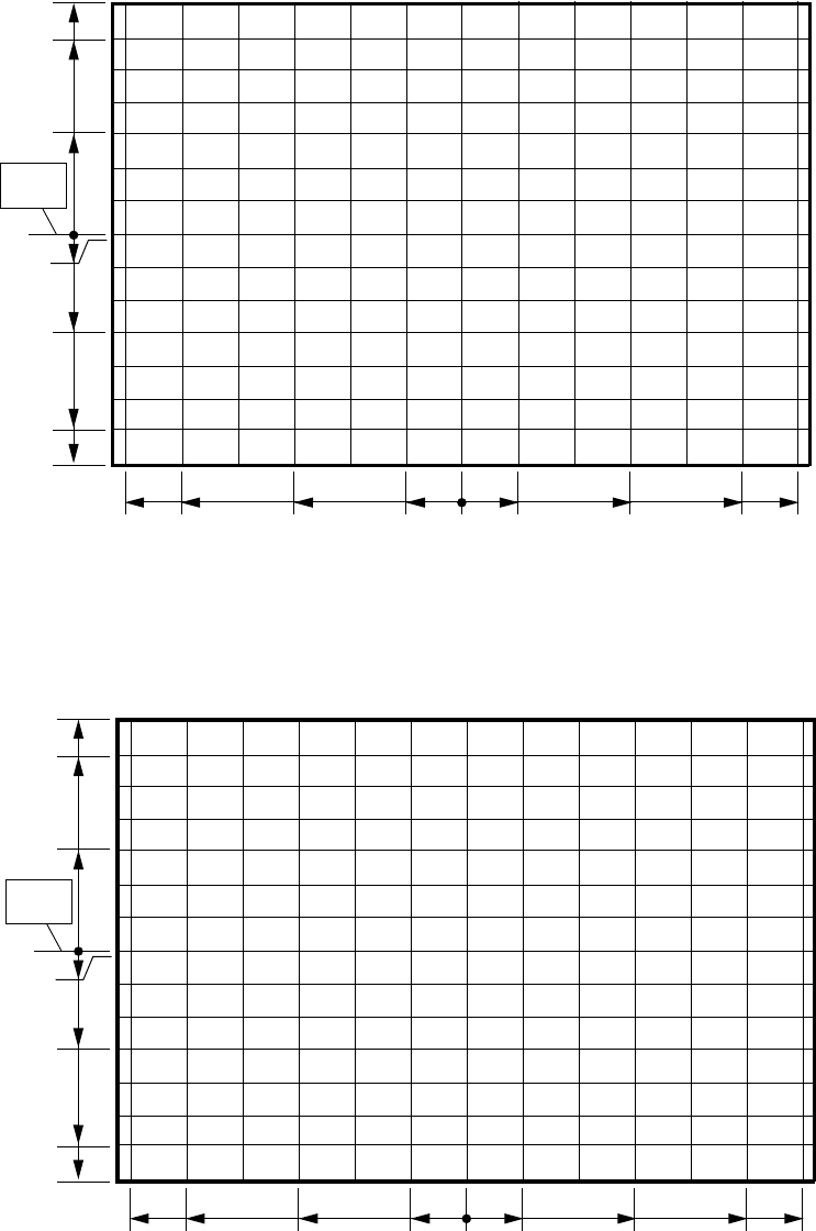
93
3-3-2. Theater Wide1
Fig. 11-7
0
428.5
351
205
66.5
428.5
351
205
66.5
249
213
103.5
0
115
217.5
249
7.5
Screen
center
40 inches 16:9 Screen size: Horizontal 885mm x Vertical 498mm
0
605
495.5
289.5
93.5
348.5
298
144
0
159
303
348.5
10
Screen
center
93.5
289.5
495.5
605
56 inches 16:9 Screen size: Horizontal 1239mm x Vertical 697mm
Fig. 11-8
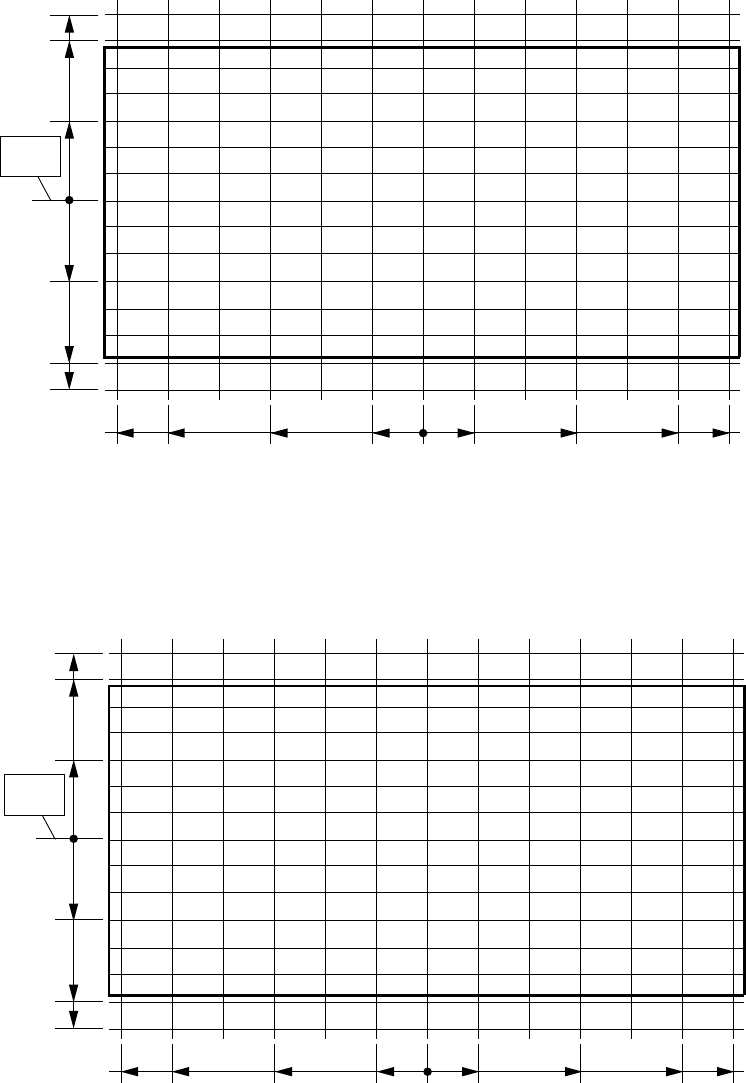
94
3-3-3. Theater Wide 2
Fig. 11-9
Fig. 11-10
0
0
298.9
256.2
128.1
435
217.5
362.5
72.5
72.5
217.5
362.5
435
Screen
center
40 inches 16:9 Screen size: Horizontal 885mm x Vertical 498mm
128.1
256.2
298.9
0
0
618
309
515
103
Screen
center
56 inches 16:9 Screen size: Horizontal 1239mm x Vertical 697mm
180.9
301.5
361.8
103
309
515
618
180.9
301.5
361.8
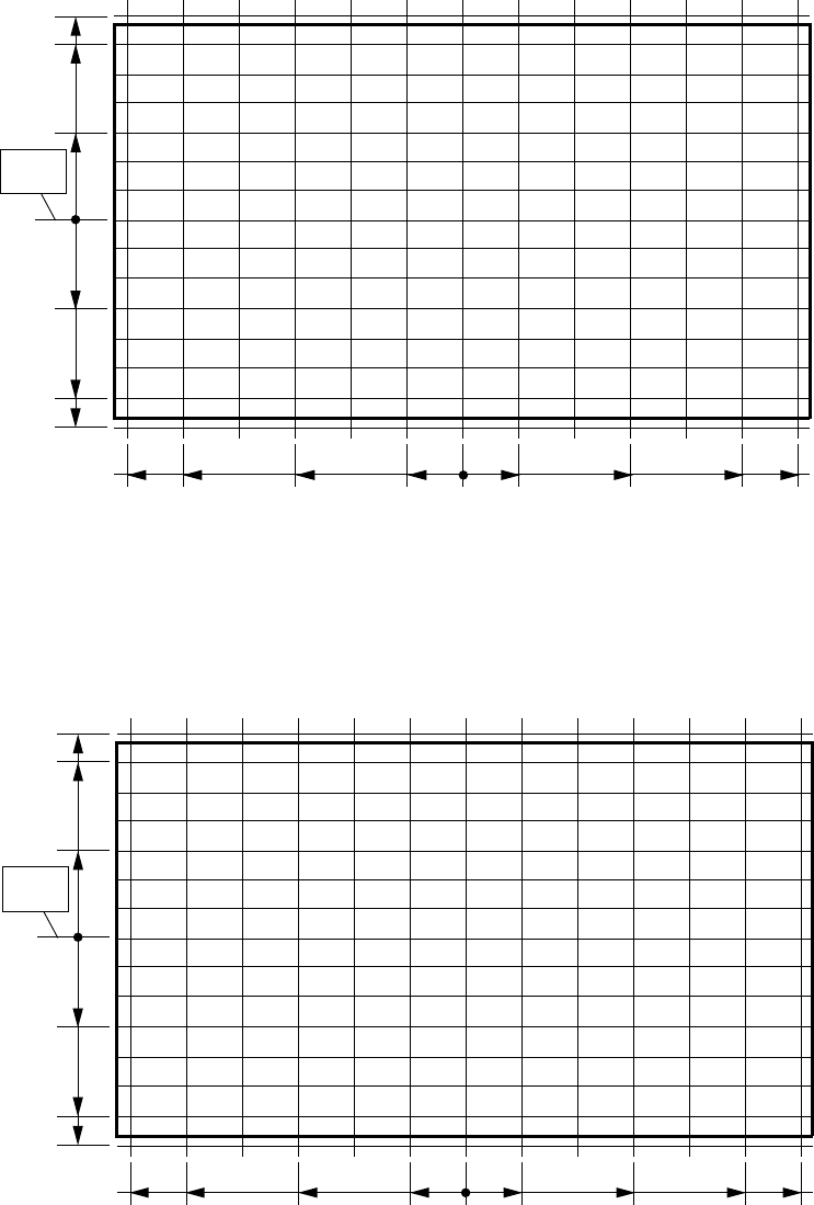
95
3-3-4. Theater Wide 3
Fig. 11-11
0
0
269.5
231
115.5
115.5
231
269.5
435
217.5
362.5
72.5
72.5
217.5
362.5
435
Screen
center
40 inches 16:9 Screen size: Horizontal 885mm x Vertical 498mm
0
0
618
309
515
103
Screen
center
56 inches 16:9 Screen size: Horizontal 1239mm x Vertical 697mm
379.2
325
162.5
162.5
325
379.2
103
309
515
618
Fig. 11-12
96
4. CASE STUDY
In many cases, a color deviation will be corrected by return-
ing the HIT and WID data for the main deflection side to the
initial values.
Followings are cases which need readjustment of the conver-
gence by all means.
4-1. When CRT is Replaced.
When the CRT is replaced, readjustment of the main deflec-
tion and color matching will be necessary. Perform the ad-
justments as follows.
(1) Replace two CRTs, blue and red.
(2) Perform horizontal adjustments for blue and red yokes
to the green CRT. Mount the yokes and velocity modu-
lation coils + alignments so that they closely touches
the CRT without any clearance.
(3) Adjust the red and blue alignments. (refer to item De-
tailed adjustments for alignments)
(4) Perform the center adjustment for the blue CRT center
and the red CRT center to the green CRT center with
the centering magnets.
(5) Adjust the HIT, WID data to obtain the data which gives
the most precision to the green.
(6) Perform the color matching in terms of the convergence
for each screen. In this case, do not move the green.
(7) After completion of the convergence adjustment for
each screen, replace the green CRT. For the green CRT,
repeat the steps 2-5 to make the color matching in terms
of the convergence by using the red and blue as the
reference.
4-2. When Convergence Unit is Replaced
When replacing the convergence units, all screens must be
adjusted basically. However, performing the adjustment as
shown below will reduce the procedures considerably.
(1) Replace the memory (Q713) for the new unit with the
memory (Q713) for the failure unit. Mount the con-
vergence unit on the set and the screen status before
replacement will be directly reproduced.
(2) Mount the new unit with the old memory installed in
combination on the set, and turn on the set. A screen as
if it is moving vertically or horizontally will appear.
(3) Adjust each center of green, red, and blue with the cen-
tering magnets again.
(4) Check to see color deviation and screen size deviation
among the colors. If deviated, perform the adjustment
for the main deflection and the color matching for the
convergence.
97
5. TROUBLESHOOTING
5-1. Adjusting Procedure in Replacing CRT
Cut off
Lens focus
Electrical focus
Yoke horizontal
User convergence enter check
Centering
Convergence adjustment
White balance
End
User convergence enter check
Centering
Convergence adjustment
End
5-2. Adjusting Procedure in Replacing Convergence Unit/Main Def
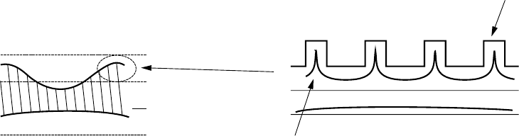
98
6. CONVERGENCE OUTPUT CIRCUIT
6-1. Outline
This circuit current-amplifies digital convergence correction
signal at output circuit, and drives by convergence yoke to
perform picture adjustment.
Digital convergence output signal 6ch adjustment is done.
(H-R/G/B) (V-R/G/B)
6-2. Circuit Description
6-2-1. Signal flow
Signal which is corrected by digital convergence, is output to
P708 (V, H R/G/B);
is input to Q751 (V) R/G/B, and is output to P713, P714 and
P715;
is input to Q752 (H) R/G/B, and is output to P713, P714 and
P715.
6-2-2. Over current protection circuit
All currents of Power supply, -15V, +15V and +30V are de-
tected to protect CONV-OUT IC from damage due to output
short of CONV-OUT.
Current value: Normal ± 15V approx. 700mA
+30V approx. 200mA
Detecting curren ±15V approx. 1.8A
or more
+30V approx. 700mA or more
protecting operation
6-2-3. Pump-up source
CONV-OUT IC Q752 (H)
Pin 10 (+15V/H, PV)
Pin 5 (+30V)
By HD input signal, pump-up is done only in horizontal re-
tracing time.
6-2-4. CONV-OUT mute
In power-on operation, transistors Q765 and Q766 are made
turned ON, and –15V is applied to pin 3 of CONV-OUT IC.
These cause mute operation on CONV-OUT.
6-2-5. Operation of IC
1) Q764 (TC74HC4050AP)
Sync signal which is input from P711 1 VD, 2 HD, is,
through buffer, supplied to digital convergence P708.
2) 3-terminal source
Q754 (+5V) Q755 (+9V) Q756 (-9V)
Source for digital convergence
3) Q767 (TC4066BP)
P711 4 SDAM, 5 SCLM : microcomputer. Busline, through
Q767, is input to Digital Convergence P709, and is controlled.
4) To adjust from outside of digital convergence :
Put adjusting jig into 6P socket of P720. Iscs turns from H to
L, switch of Q767 is changed over. Then busline from mi-
crocomputer is cut off.
P720 3 SCLU, 4 SDAU
Controlled by external adjusting jig.
+30V
+15V
0V
-15V
+30V
+15V
0V
-15V
Horizontal correction wafeform Pump-up source waveform
Pump-up
Horizontal correction waveform
Fig. 11-13
99
6-3. Convergence Block Diagram
Fig. 11-14
DIGITAL CONVER
P708
RV
GV
BV
RH
GH
BH
+9V
-9V
+5V
HD
VD
R
G
B
I2CS
SCLV
SDAU
SCLM
SDAM
(REGULATER)
Q754
+5V
Q755
+9V
Q756
-9V
Q764
TC74HC4050
(HD)
Q767
TC4066BP
P720
P711
1
2
3
4
5
6
7
+
C7766
Q766
MUTE
+30V
B-H G-H R-H
-15V
B-V G-V R-V
+
C7765
MUTE
510
9
8
4
3
11
12
18
17
Q765
510
9
8
4
3
11
12
18
17
CONV-OUT
CONV-OUT
(+1501
H.PU) (H)
Q752
STK392-110
V
H
Q751
STK392-110
P715
GREEN
V
H
P714
BLUE
V
H
P713
RED
C7771
(HD) Q769
Q770
Q771
(PUMP UP)
+15V
D7702
D7701 Q757
5V-1
(PROTECTOR) R7782
0.82Ω
(+30V)
R7750
0.33Ω
(+15V)
R7765
0.39Ω
(-15V)
CONVER
YOKE
VD
HD
I CS
SDAM
SCLM
GND
DFAI
2
1
2
3
4
5
6
GND
INCS
SCLU
SDAU
GND
GND
1
2
3
1
2
3
4
5
+12V
NC
PROTECT
+5V-1
RESET
POWER
AC PULSE
GND
P712
P
100
7. CONVERGENCE TROUBLESHOOTING CHART
Fig. 11-6
Pump-up
Convergence output signals correction wave
+30V
-15V
0V
Vertical
Q751
(R/G/B)
Horizontal
Q752
(R/G/B)
Reray OFF Reray ON
Reray ON
Reray ON
Reray OFF Reray OFF
NG
NG
NG
OK
OK
OK
OK
OK
Protect 1
Relay turns on
once but immediately
turns off.
Relay operation sound
at power on.
No Convergence
correction wave.
Check screen modes
of picture.
Convergence PCB,
pull out of P712.
Check power
supply circuit. Check Q751, Q752
and repair.
Reray OFF
Proceed to "protection
circuit diagnosis procedures".
Check P708 R/G/B
correction wave.
Check voltage at
±15V+30V pump up. Check power supply
circuit.
Are output signals
applied to H, Vblk of P711. Check DEF PC13.
Check voltage across
±9V+5V Q754, Q755, Q756. Check Q754, Q755,
Q756 and repair.
Check signals of all IC
and associated cirduits.
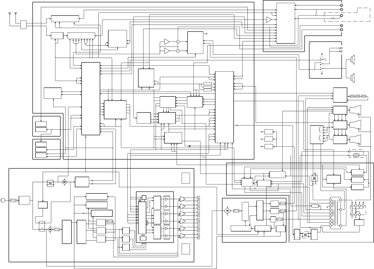
RF
SW
H003
ANT1
ANT2
HY01
TUNER/IF
SCL SDA ATF2 TV2-V
TUNER
SCL SDA
H001 H002
TUNER
SDASCL
ATF1RWL L R
TV1-V, L, R
FRONT
SURROUND
UNIT
L
R
L
R
SURROUND
SW
AFT2
AFT1
I C STOP
SCL
SDA
2
MUTE
INT/EXT
SYNC-AV1
YS/YM
I C STOP
2
DVD SW
SYNC VCD
CLK
CS
BUSY
DATA
OSD RST
HD
VD
RESET
+5V-1
POWER
SCL 0
SDA 0
ACP
KEY A
KEY B
RMT OUT
RMT
TMP87CS38N
-3320
QA01
MICROCOMPUTER
MEMORY
EEPROM SCL 0
SDA 0
+5V-1
QA02
SDASCL V-AV
YS
R
G
B
CLK
CS
BUSY
DATA
OSD RST
HD VD
OSD/EDS/
CC/RGB SW
UNITCP
24LC088 I/P
VIDEO 3
INPUT
FRONT
KEYS
FRONT
UNIT
POWER
SWITCH
PHOTO
DIODE
REMOTE
SENSOR
FRONT
UNIT
SUB
V
C
Y
Y/C
SEP.
ZY01 CFM113
SCL
SDA
SUPER
LIVE
NORMAL
WIDE
BLK
AUTO LIVE
UNIT
SCP
SCL
SDA
Y
C
VD
HD
SCP
Y
I
Q
DUAL
UNIT
SCL
SDA
VP
HD
Y
I
Q
YIQ
VD
BLK
3D. Y/C
SEPA.
UNIT
WAC
UNIT
Y
I
Q
SWY Y
I
Q
Cr Cd
DVD SW
UNIT
CSP
SCL SDAC
Y
Y.C VIDEO
BUFFER
BUFFER
BUFFER
Y
C
V-AV
QS101
QS101
+
+
W(SBS)
R
L
FRONT
LAMP
LA4282
L
+38V
R
MUTE
Q601
B
G
R
SCP
OSD B
OSD G
OSD R
OSD Y5
Q
I
Y
Q
I
Y
SYNC OUT
C-IN
SYNC IN
Y-IN
SDA
SCL
H-OUT
ABL
V.S.M.
B
G
R
Y
S
Ym/Power off
VIDEO/
CHROMA
TA1222AN
Q501
FBP
VP-OUT
HD-OUT
+9V
+5V-2
+5V-3
+9V-2
Q830
Q831
Q832
TV2
SCL
SDA
TV1
(V.L.R)
SYNC-AV1
L.R
V3(V.Y.C.L.R)
PIP-V
Y.C
V-AV
Y.C
V1
V2
DVD IN
TA1218N
QV01
A\V
SW
A/V
UNIT
VIDEO2(Y,L,R or DVD (L,R)
DVD (Y, Cr, Cb) DVD (Y)
VARI OUT (L,R)
MONITOR OUT (V, L, R)
CVD (Cr, Cb)
VIDEO2
(V.L.R) or
DVD (Y.L.R)
VIDEO1 (V, Y, C, L, R)
DVD (Y,L,R)
S601
EXT
EXT SP
FRONT
HEATER
INT
EXT
SPEAKER
UNIT
L, R
L
R
FRONT SP
OR CENTER SP
EXT SP (L) FRONT
EXT SP (R) FRONT
FRONT
+200V
BLK
V.S.M
+125V
+12V
DRIVE
RETURN
S.V.M
UNIT L472
(R) L473
(G) L474
(B)
V.M. COIL
ORT DRIVE
(RED)
UNIT
V901
PICTURE
TUBE (RED)
V902
PICTURE
TUBE (GREEN)
V903
PICTURE
TUBE (BULE)
30.7kV
30.7kV
30.7kV
ORT DRIVE
(GREEN)
UNIT
ORT DRIVE
(BULE)
UNIT
V
H
DEF YORK
L462, L463, K464
Z410
R
G
B
R
G
B
TO CRT
FOCUS
(G4)
TO CRT
SCREEN
(G2)
FUCAS PACK
DOF Eo
AC120V
60Hz
F801
125V7A LINE
FILTER
TRF3205M
T801
T802
RELAY
DRIVE
QB43 QB30
T840
TPW1459AZ
POWER
RELAY
SR81
DC12VTV-8
D802-D805
F850
125V3.15A
VOLTAGE REG.
STR57041
Q802
CONVERTER TRANS
TPW3330AM
T888
D840
S1WA20
STANDBY
+5V REGU
L78MR05
STB5V
RESET
OVER CURRENT
PROTECT
OVER VOLTAGE
PROTECT
LOW VOLTAGE
PROTECT
+30V
+15V
-15V
F851 125V5A
Q755
Q754
Q756
-9V
+5V
+9V
L462
RED
CONVER
YOKE
L462
BLUE
CONVER
YOKE
L462
GREEN
CONVER
YOKE
RH
BH
GH
Q752
STK392-110
AMP
GH
GH
BH
BH
RH
RH
STK392-110
RV
BV
GV
Q751
CONVER OUTPUT
AMP
Q707 Q703 Q715
PLL
Q701
DIGITAL
CONNER
T7064
DIGITAL CONVERGENCE LNIT
DAC
DAC
DAC
Q705
Q704
Q713
Q717
Q719
PHOTO COUPLER
TLP621 (GR-L)
+125V
VOLTAGE REG.
STR-Z23201
CONVERTER
TRANS TPW3332A5
PROTECTION
HIC1019
OVER
VOLTAGE
PROTECT
+38V
+12V
Q801 Q862
Z801Z862
X-TAL
125V5A
F860
125V5A
F890
125V5A
F889
250V2A
F870
D801
POWER1
UNIT
POWER
PROTECT
SCL
SDA
VD
DPC WF
+9V
+35V
-27V
DPC
UNIT Q301
V-BLK
VERTICAL
LA78335
IN OUT
Q487, Q488, Q489
V-BLK BLK
H-BLKV-STOP
BLANKING
DQF
T400
AFC
HEATER
ABL SELECT
NORMAL
Q420
+9V-1
10
9
4
7
6
5
2
3
18
+12V
+35V
-27V
+125V
+125V
ABL
FOCLS
HV
T461 FBT
TFB3078AD
DEF H.V UNIT
Q402
HOR.
DRIVE
Q404
HOR.
OUT
2SC1589
Q401
2SC2253FA
HV REGU.
CIRCUIT
Q483, Q480
Z450 CR BLOC
K
TPA5007
H-5
CORECTION
SUPER LIVE
WF
CIRCUIT
WIDE WIDE
V-SHIFT
MAIN UNIT
