TranSystem 40600028B01 Bluetooth UART/PCM RF Module User Manual
TranSystem Bluetooth UART/PCM RF Module
UserManual.wiki
>
TranSystem
>
40600028B01 User Manual
User Manual
Navigation menu
Upload a User Manual
Namespaces
Wiki Guide
HTML
PDF
Info
Views
User Manual
Discussion / Help
Navigation

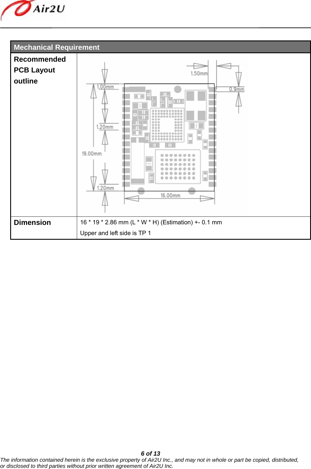
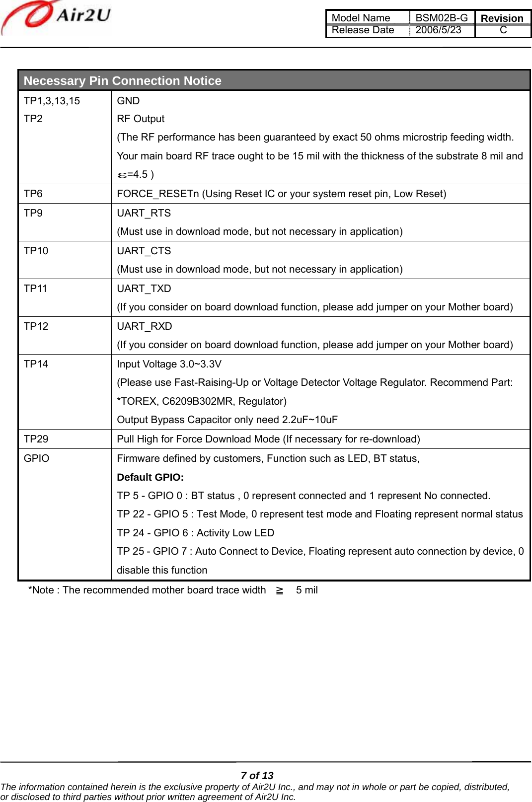
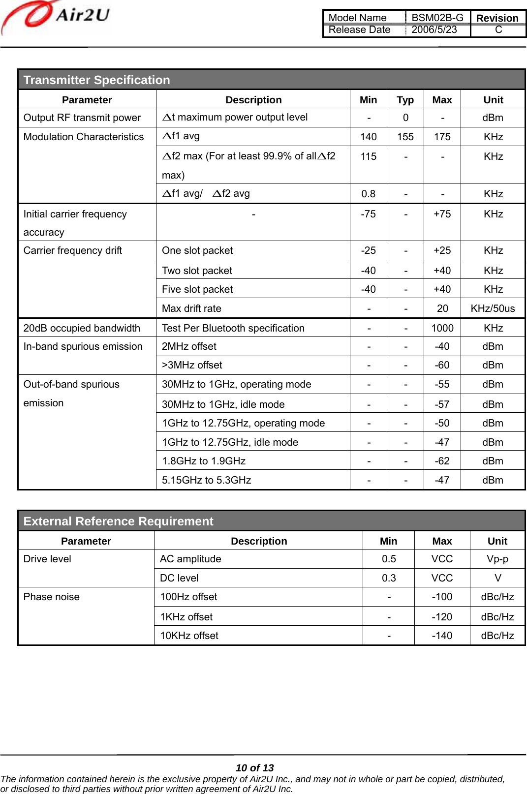
![Model Name BSM02B-G RevisionRelease Date 2006/5/23 C Operation Description (Pin assignment) TP 1 TP 2 TP 3 TP 4 TP 5 TP 6 TP 7 TP 8 TP 9 TP 10 TP 11 TP 12 TP 13 TP 14 TP 15 GND RF Output GND NC MFP[0] FORCE_RESETn HOST_WAKE EXT_WAKE UART_RTS UART_CTS UART_TXD UART_RXD GND +(Vcc) GND NC PCM_CLK PCM_SYNC PCM_IN PCM_OUT MFP[3] MFP[5] MFP[4] MFP[6] MFP[7] AUX_TXD ADC_IN PWR_REG_EN FORCE_Download NC TP 16 TP 17 TP 18 TP 19 TP 20 TP 21 TP 22 TP 23 TP 24 TP 25 TP 26 TP 27 TP 28 TP 29 TP 30 PIN PIN NameTypeDescription TP1,3,13,15 GND GND Module Ground TP2 RF Output Bi-Dir Output TX/RX TP5 MFP[0] CMOS Bi-Dir Programmable I/O line TP6 FORCE RESETn CMOS input Sytem Reset TP7 MFP[1]/HOST WAKE CMOS Bi-Dir Programmable I/O line TP8 EXT WAKE CMOS input Wake upsignal from host TP9 UART RTS CMOS output UART ready to send TP10 UART CTS CMOS input UARTclear to send TP11 UART TXD CMOSoutputUARTdata output TP12 UART RXD CMOS input UARTdata input TP14 +(Vcc) VDD Module Power TP17 PCM CLK CMOS Bi-Dir Synchronous data clock TP18 PCM SYNC CMOS Bi-Dir Synchronous data strobe TP19 PCM IN CMOS input Synchronous data input TP20 PCM OUT CMOS output Synchronous dataoutput TP21 MFP[3] CMOS Bi-Dir Programmable I/O line TP22 MFP[5] CMOS Bi-Dir Programmable I/O line TP23 MFP[4] CMOS Bi-Dir Programmable I/O line TP24 MFP[6]/AUX RXD CMOS Bi-Dir Programmable I/O line TP25 MFP[7] CMOS Bi-Dir Programmable I/O line TP26 AUX TXD CMOS Bi-Dir Programmable I/O line TP27 ADC IN AnalogAto D converter input TP28 PWR REG IN CMOS Bi-Dir Enable for external regulatorTP29 FORCE Download CMOS input Force to download mode 5 of 13 The information contained herein is the exclusive property of Air2U Inc., and may not in whole or part be copied, distributed, or disclosed to third parties without prior written agreement of Air2U Inc.](https://usermanual.wiki/TranSystem/40600028B01/User-Guide-731163-Page-6.png)