TranSystem 40600028B01 Bluetooth UART/PCM RF Module User Manual
TranSystem Bluetooth UART/PCM RF Module
User Manual

Model Name BSM02B-G Re
v
ision
Release Date 2006/5/23 C
Data
Sheet
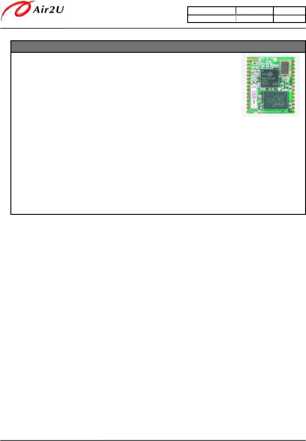
Model Name : BSM02B-G
Product Name : Bluetooth UART/PCM RF Module
威譜通訊股份有限公司
Air2U
Inc.
新竹市科學園區工業東四路
1
9
號
4
樓
4F, No. 19 Industry E. RD 4, Hsinchu Science Park, Hsin-Chu 300, Taiwan, R.O.C
Tel: 886-3-567-8877 Fax: 886-3-563-2233
http : // www.air2u.com.tw
The information contained herein is the exclusive property of Air2U Inc., and may not in whole or part be copied, distributed, or
disclosed to third parties without prior written agreement of Air2U Inc.

Model Name BSM02B-G Re
v
ision
Release Date 2006/5/23 C
History
Date Rev. Description
2006/3/22 A First release
2006/5/17 B Upgrade to BT V2.0
2006/5/23 C Modify “Application Example”
Add “Reference Circuit Design: Download Tool”
Add “Reference Circuit Design: PCM Application”
1 of 13
The information contained herein is the exclusive property of Air2U Inc., and may not in whole or part be copied, distributed,
or disclosed to third parties without prior written agreement of Air2U Inc.
Model Name BSM02B-G Re
v
ision
Release Date 2006/5/23 C
Product
Overview
The Air2U universal Class2 Bluetooth Module BSM02B-G is a compact and BQB
qualified module that provides a complete 2.4GHz Bluetooth system for data and
voice communications. This module is optimized for fast implementation in various
applications to enable electronic devices to communicate wirelessly with other
Bluetooth enabled devices. For example, the module can be used in applications
such as Laptop PC, PC accessories, PDA, access points and other embedded
integration applications. The BSM02B-G, Air2U’s core universal class2 Bluetooth
Module, comes without an antenna or connector and is designed to operate in
commercial temperature range. Extra reference designs, such as a class1 device
design or a system antenna integration design can also be supported by Air2U to
meet customers’ specific requirements. Standard software for the BSM02B-G
Bluetooth module includes the lower layer protocol stack software up to the host
interface (HCI). The upper layer protocol stacks, profiles, and application software
are also available directly from Air2U in a case by case design base. This module
also complies with RoHS instructions.
2 of 13
The information contained herein is the exclusive property of Air2U Inc., and may not in whole or part be copied, distributed,
or disclosed to third parties without prior written agreement of Air2U Inc.

Model Name BSM02B-G Re
v
ision
Release Date 2006/5/23 C
Features
a
Radio Transceiver
1. Typical –80 dBm receiver sensitivity under high interference environment
2. Output power ranges from 0~2dBm RF transmit power with level control
a
BaseBand
1. Compliant with Bluetooth V 2.0 including AFH and extended SCO
2. Standard HCI interface
3. Piconet and scatternet with support for up to 7 active connections.
4. Powerful 32-bit ARM7TDMI processor with ability to execute complete voice algorithms without separate
DSP
5. Low current CMOS technology reduces standby current consumption.
6. Extensive multi function I/Os allow flexible application usage
7. Software execution from external flash memory or internal ROM with patching capability.
8. Channel Quality Driven Data Rate controls multi-slot packets to minimize packet overhead and maximize
data throughput.
9. Built-in UltimateBlue Coexistence Software reduces interference to 802.11 devices.
a
Physical Interfaces
1. Standard HCI interface (UART) with programmable baud rate (9.6k, 19.2k, 38.4k, 57.6k, 115.2k, 230.4k,
460.8k, 500k, 921.6k, 1M, 1.5M, 2M) and flow control
2. Audio Codec Interface can be configured to support:
a. Standard 64KHz PCM clock rate and up to 2.048MHz clock rates with support for multi-slot
handshakes and synchronization
b. Motorola SSI mode
c. Either master or slave mode
d. Support 8, 13, 14, and 16-bit PCM data
3. Up to 8 multi-function I/O ports are available
4. I2C bus can be configured and enabled to interface and control external I2C devices. The I2C bus is
controlled by the application software.
5. Auxiliary ADC is available for application usage such as battery level detection or position sensing
a
Package Option
SMD Type
3 of 13
The information contained herein is the exclusive property of Air2U Inc., and may not in whole or part be copied, distributed,
or disclosed to third parties without prior written agreement of Air2U Inc.

Model Name BSM02B-G Re
v
ision
Release Date 2006/5/23 C
Summary of Benefits
a
Complete Bluetooth Solution
1. A single-chip processor IC combines complete 2.4GHz Radio Transceiver, baseband and protocol stack
software for Bluetooth wireless technology
2. RFMD 3500, single chip Bluetooth system with 0.18um low power CMOS technology
3. Complex audio algorithms such as noise canceling algorithms for improved audio performance are also
available for integration
4. Fully V2.0 BQB qualified
5. Simplify overall design and development cycle
6. Full speed class2 Bluetooth operation with full 7 slave piconet support
7. Provides an open platform for the development of upper layer protocol stack, profiles and application
software
a
Radio Features
1. Direct conversion architecture with outstanding receiver blocking performance
2. On chip 50ohm matching network requires no external impedance matching components
3. Clock_Request signals are available allowing control of external clock source during low power states
4. Low out of band spurious emission
a
Baseband and Standard Protocol Stack Features
1. Powerful ARM7TDMI processor core with up to 32MIPs of total CPU resource.
2. Full-featured protocol stack from link manager up to and including the host interface (HCI)
3. Full support of low power park and sniff with selectable sniff internals of match system wake/sleep cycles
4. Verified compatibility with multiple upper layer stack software
5. Low power connection states with hold, sniff, and park modes.
6. Low power standby modes to enable very efficient power management
a
Application
1. PC, Notebooks, printers, Mobile phone, PDAs
2. GPS and Navigator
3. Cordless headsets, digital camera
4. Computer Accessories
5. Many other computer peripherals or embedded devices applications
a
Support Profiles
Headset Gateway Profile (HSP), Hands Free Gateway Profile (HFP), Serial Port (SPP), Human Interface
Device Profile (HID)
4 of 13
The information contained herein is the exclusive property of Air2U Inc., and may not in whole or part be copied, distributed,
or disclosed to third parties without prior written agreement of Air2U Inc.
Model Name BSM02B-G Re
v
ision
Release Date 2006/5/23 C
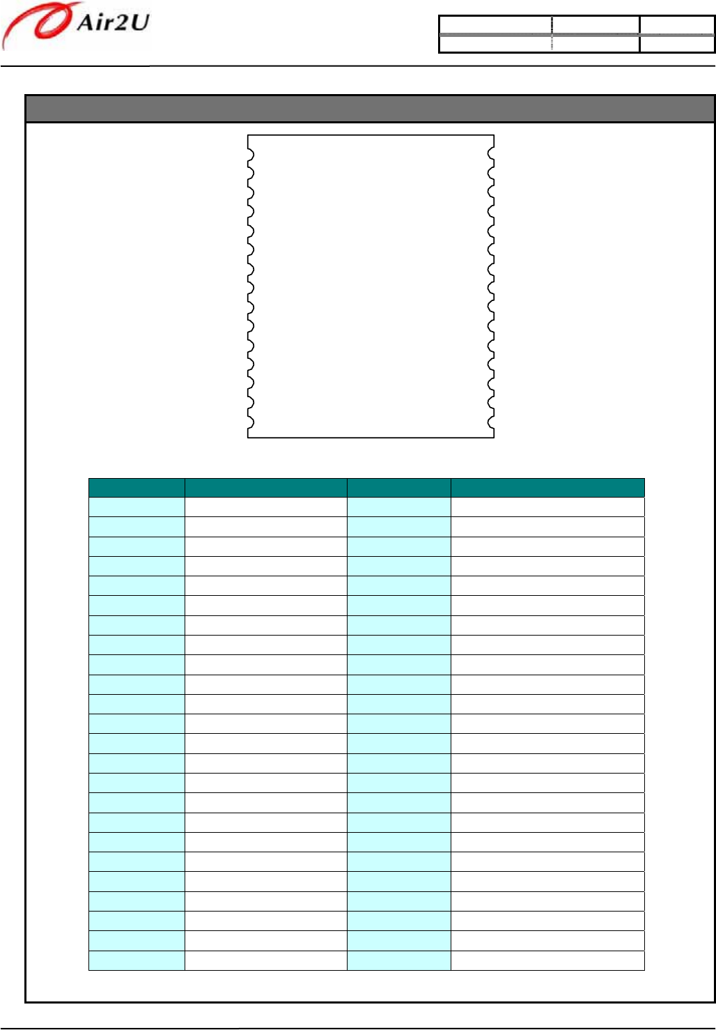
Operation Description (Pin assignment)
TP
1
TP
2
TP
3
TP
4
TP
5
TP
6
TP
7
TP
8
TP
9
TP
10
TP
11
TP
12
TP
13
TP
14
TP
15
GND
RF
Output
GND
NC
MFP[0]
FORCE_RESETn
HOST_WAKE
EXT_WAKE
UART_RTS
UART_CTS
UART_TXD
UART_RXD
GND
+(Vcc)
GND
NC
PCM_CLK
PCM_SYNC
PCM_IN
PCM_OUT
MFP[3]
MFP[5]
MFP[4]
MFP[6]
MFP[7]
AUX_TXD
ADC_IN
PWR_REG_EN
FORCE_Download
NC
TP
16
TP
17
TP
18
TP
19
TP
20
TP
21
TP
22
TP
23
TP
24
TP
25
TP
26
TP
27
TP
28
TP
29
TP
30
PIN PIN Name
T
y
p
eDescri
p
tion
TP1
,
3
,
13
,
15 GND GND Module Ground
TP2 RF Out
p
ut Bi-Dir Out
p
ut TX/RX
TP5 MFP
[
0
]
CMOS Bi-Dir Pro
g
rammable I/O line
TP6 FORCE RESETn CMOS in
p
ut S
y
tem Rese
t
TP7 MFP
[
1
]
/HOST W
A
KE CMOS Bi-Dir Pro
g
rammable I/O line
TP8 EXT W
A
KE CMOS in
p
ut Wake u
p
si
g
nal from host
TP9 U
A
R
T
R
TS CMOS out
p
ut U
A
R
T read
y
t
o send
TP10 U
A
R
T CTS CMOS in
p
ut U
A
R
Tclear to send
TP11
U
A
R
T TXD
C
M
OS
out
p
ut
U
A
R
Tda
t
a ou
t
p
ut
TP12 U
A
R
T R
X
D CMOS in
p
ut U
A
R
Tda
t
a in
p
ut
TP14 +
(
Vcc
)
VDD Module Power
TP17 PCM CLK CMOS Bi-Dir S
y
nchronous da
t
a clock
TP18 PCM SYNC CMOS Bi-Dir S
y
nchronous da
t
a s
t
robe
TP19 PCM IN CMOS in
p
ut S
y
nchronous da
t
a in
p
ut
TP20 PCM OUT CMOS out
p
ut S
y
nchronous da
t
aout
p
ut
TP21 MFP
[
3
]
CMOS Bi-Dir Pro
g
rammable I/O line
TP22 MFP
[
5
]
CMOS Bi-Dir Pro
g
rammable I/O line
TP23 MFP
[
4
]
CMOS Bi-Dir Pro
g
rammable I/O line
TP24 MFP
[
6
]
/AUX RXD CMOS Bi-Dir Pro
g
rammable I/O line
TP25 MFP
[
7
]
CMOS Bi-Dir Pro
g
rammable I/O line
TP26
A
UX TXD CMOS Bi-Dir Pro
g
rammable I/O line
TP27
A
DC IN
A
nalo
g
A
to D converter in
p
ut
TP28 PWR REG IN CMOS Bi-Dir Enable for e
x
ternal re
g
ulator
TP29 FORCE Download CMOS in
p
ut Force to download mode
5 of 13
The information contained herein is the exclusive property of Air2U Inc., and may not in whole or part be copied, distributed,
or disclosed to third parties without prior written agreement of Air2U Inc.
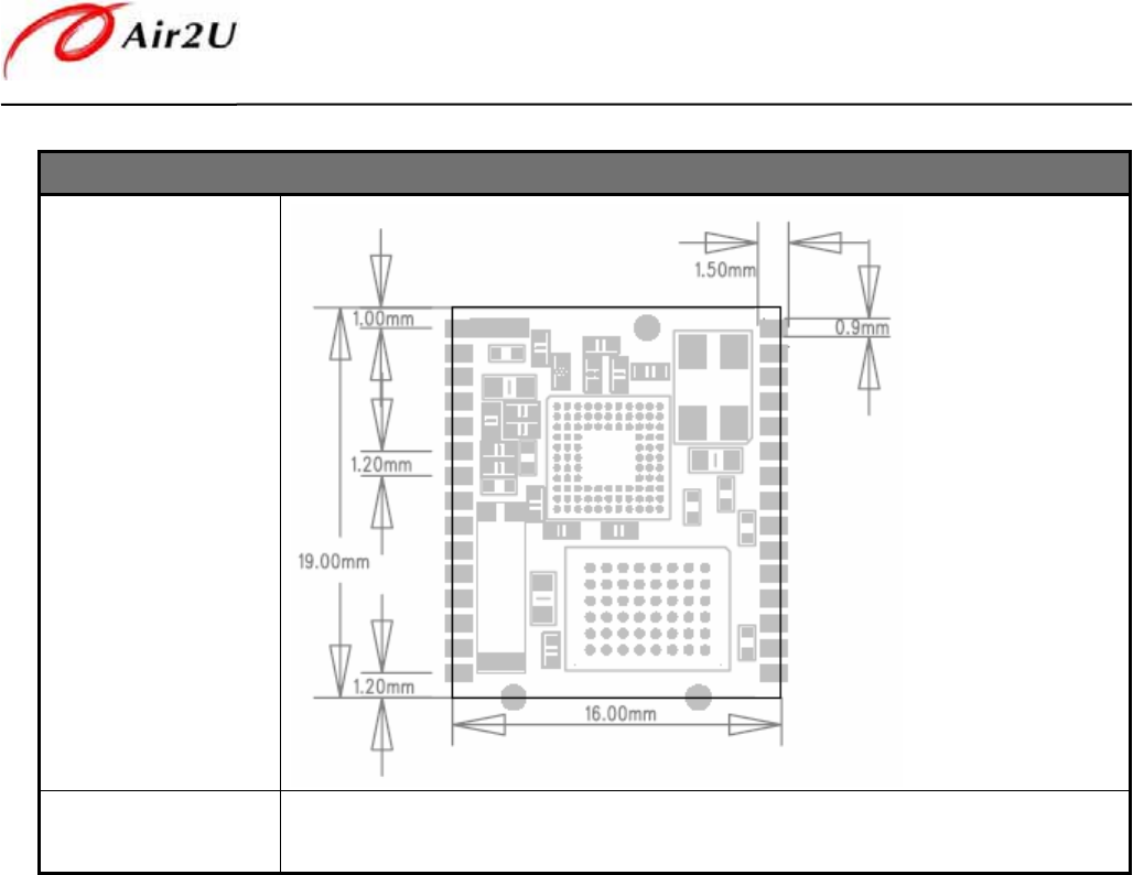
Mechanical Requirement
Recommended
PCB Layout
outline
Dimension 16 * 19 * 2.86 mm (L * W * H) (Estimation) +- 0.1 mm
Upper and left side is TP 1
6 of 13
The information contained herein is the exclusive property of Air2U Inc., and may not in whole or part be copied, distributed,
or disclosed to third parties without prior written agreement of Air2U Inc.

Model Name BSM02B-G Re
v
ision
Release Date 2006/5/23 C
Necessary Pin Connection Notice
TP1,3,13,15 GND
TP2 RF Output
(The RF performance has been guaranteed by exact 50 ohms microstrip feeding width.
Your main board RF trace ought to be 15 mil with the thickness of the substrate 8 mil and
ε
=4.5 )
TP6 FORCE_RESETn (Using Reset IC or your system reset pin, Low Reset)
TP9 UART_RTS
(Must use in download mode, but not necessary in application)
TP10 UART_CTS
(Must use in download mode, but not necessary in application)
TP11 UART_TXD
(If you consider on board download function, please add jumper on your Mother board)
TP12 UART_RXD
(If you consider on board download function, please add jumper on your Mother board)
TP14 Input Voltage 3.0~3.3V
(Please use Fast-Raising-Up or Voltage Detector Voltage Regulator. Recommend Part:
*TOREX, C6209B302MR, Regulator)
Output Bypass Capacitor only need 2.2uF~10uF
TP29 Pull High for Force Download Mode (If necessary for re-download)
GPIO Firmware defined by customers, Function such as LED, BT status,
Default GPIO:
TP 5 - GPIO 0 : BT status , 0 represent connected and 1 represent No connected.
TP 22 - GPIO 5 : Test Mode, 0 represent test mode and Floating represent normal status
TP 24 - GPIO 6 : Activity Low LED
TP 25 - GPIO 7 : Auto Connect to Device, Floating represent auto connection by device, 0
disable this function
*Note : The recommended mother board trace width ≧ 5 mil
7 of 13
The information contained herein is the exclusive property of Air2U Inc., and may not in whole or part be copied, distributed,
or disclosed to third parties without prior written agreement of Air2U Inc.
Model Name BSM02B-G Re
v
ision
Release Date 2006/5/23 C
Environment Test Specification
1 Operation Temperature -10℃ ~ 60℃
2 Storage Temperature -20℃ ~ 80℃
3 Operation Humidity 10% ~ 90% No condensing
4 Storage Humidity 10% ~ 90% No condensing
Certified
1 EMC CE, FCC (Pre-certified)
2 Bluetooth BQB
Current Consumption
Operating Mode Average Unit
Standby 20 uA
Parked slave, 1.28sec, interval 70 uA
Page/Inquiry scan, 1.28sec, interval 1.1 mA
ACL connection, sniff mode, 40 ms interval 1.3 mA
ACL data transfer 723 kbps TX, 57 kbps RX, DH5 continuous packets 42 mA
SCO connection, HV3 packets 22 mA
8 of 13
The information contained herein is the exclusive property of Air2U Inc., and may not in whole or part be copied, distributed,
or disclosed to third parties without prior written agreement of Air2U Inc.
Model Name BSM02B-G Re
v
ision
Release Date 2006/5/23 C
Receiver Specification
Parameter Description Min Typ Max Unit
Receiver sensitivity BER< 0.1% - -80 - dBm
Max usable signal BER< 0.1% -10 0 - dBm
C/I co-channel (0.1%BER) Co-channel selectivity - 8.0 10.0 dB
C/I 1MHz (0.1%BER) Adjacent channel selectivity - -4.0 -3.0 dB
C/I 2MHz (0.1%BER) 2
nd
adjacent channel selectivity - -38.0 -35.0 dB
C/I >=3MHz (0.1%BER) 3
rd
adjacent channel selectivity - -43 -40 dB
30 MHz – 2000 MHz -10 - - dBm
2000MHz – 2399 MHz -27 - - dBm
2498 MHz – 3000 MHz -27 - - dBm
Out-of-band blocking
3000MHz – 12.75 GHz -10 - - dBm
Intermodulation Max interferer level to maintain
0.1%BER, interference signals at 3
and 6 MHz offset
-39 -36 - dBm
30 MHz to 1 GHz - - -57 dBm Receiver spurious emission
1GHz to 12.75GHz - - -47 dBm
Note:
1. Measured into the chip with 50ohms source and no bandpass filter
2. Nominal and extreme Bluetooth test conditions as defined by the BT SIG published RF test spec 2.0
3. Out-of-band blocking guaranteed by design
4. Except receive channel sub harmonics
9 of 13
The information contained herein is the exclusive property of Air2U Inc., and may not in whole or part be copied, distributed,
or disclosed to third parties without prior written agreement of Air2U Inc.
Model Name BSM02B-G Re
v
ision
Release Date 2006/5/23 C
Transmitter Specification
Parameter Description Min Typ Max Unit
Output RF transmit power
∆
t maximum power output level - 0 - dBm
∆
f1 avg 140 155 175 KHz
∆
f2 max (For at least 99.9% of all
∆
f2
max)
115 - - KHz
Modulation Characteristics
∆
f1 avg/
∆
f2 avg 0.8 - - KHz
Initial carrier frequency
accuracy
- -75 - +75 KHz
One slot packet -25 - +25 KHz
Two slot packet -40 - +40 KHz
Five slot packet -40 - +40 KHz
Carrier frequency drift
Max drift rate - - 20 KHz/50us
20dB occupied bandwidth Test Per Bluetooth specification - - 1000 KHz
2MHz offset - - -40 dBm In-band spurious emission
>3MHz offset - - -60 dBm
30MHz to 1GHz, operating mode - - -55 dBm
30MHz to 1GHz, idle mode - - -57 dBm
1GHz to 12.75GHz, operating mode - - -50 dBm
1GHz to 12.75GHz, idle mode - - -47 dBm
1.8GHz to 1.9GHz - - -62 dBm
Out-of-band spurious
emission
5.15GHz to 5.3GHz - - -47 dBm
External Reference Requirement
Parameter Description Min Max Unit
AC amplitude 0.5 VCC Vp-p Drive level
DC level 0.3 VCC V
100Hz offset - -100 dBc/Hz
1KHz offset - -120 dBc/Hz
Phase noise
10KHz offset - -140 dBc/Hz
10 of 13
The information contained herein is the exclusive property of Air2U Inc., and may not in whole or part be copied, distributed,
or disclosed to third parties without prior written agreement of Air2U Inc.
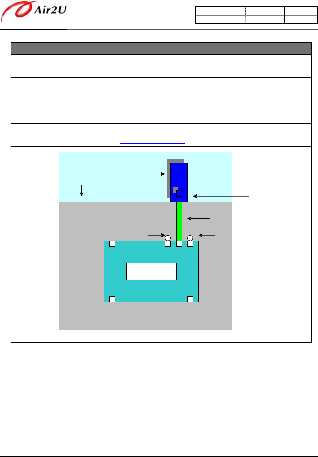
BSM02B-G Module External Antenna Application Note
1 P/N ACX AT9520-B2R4HAAB
2 Frequency Range 2.4~2.5GHz
3 Peak Gain 3.0dBi typ.
4 Average Gain 1.0dBi typ.
5 VSWR @ BW 2.0 max.
6 Impedance 50 ohm
7 Size 9.5 X 2.0 mm Monolithic SMD
8 Web Site http://www.acxc.com.tw
9
Antenna must mount on the substrate
without any metal at all layers
Vertical to the Ground Plane
Ground Plane 50 ohms impedance is necessary and it depends
thickness of the substrate ( 8 mil for
ε
=4.5)
TP1 and TP3 are absolutely necessary
TP15
TP3
TP2
Ground is necessary to via
Siw3500 Module
TP30
TP16
Model Name BSM02B-G Re
v
ision
Release Date 2006/5/23 C
on
*Note-1 : The detailed spec was shown at datasheet.
*Note-2 : The RF performance has been guaranteed by exact 50 ohms microstrip feeding width. It is known that
the width is 15 mil when the thickness of the substrate is 8 mil and ε=4.5. If you don’t make sure the
feeding width of your board, please contact with our engineer.
11 of 13
The information contained herein is the exclusive property of Air2U Inc., and may not in whole or part be copied, distributed,
or disclosed to third parties without prior written agreement of Air2U Inc.
TP
29,
Force_Download
Siw3500
Module
UART
Signal
Pins,
TP9,
TP10,
TP11,
TP12
Model Name BSM02B-G Re
v
ision
Release Date 2006/5/23 C
Application example
Download Process
To
VCC
UART
Signal
CTS,
RTS,
TX,
RX
Signal
Converter
Board
RS232
Cable
Reserve for Download
(Suggestion)
PC
You can force SiW3500 module to download mode. In this mode, you can
download the firmware and nvm parameter. The procedure to force the module to
download mode are
1. Connect TP9~12 to “Signal Converter Board”. (This board can be provided from
Air2U.)
2. Connect TP29 to VCC.
3. Connect RS232 cable between “Signal Converter Board” and PC.
4. Give the power to SiW3500 module. (SiW3500 module’s VCC and GND can be
shared with Signal Converter Board’s.)
5. In PC side, launch the download program provided by Air2U.
If it is necessary to upgrade firmware, you need to reserve some components on
your board as:
Connect w/ device
For normal customer’s usage, R1~R4 should be mounted and J1 can be
non-mounted. Once you need to upgrade firmware, you can mount J1 and remove
R1~R4. Then, follow “Download Process” as above,
Output
,
TP
5
,
Sta
tus
I
ndi
ca
to
r
Si
w3500
Modul
e
GP
S
Output
,
TP2
4
,
Activity
LED
TP1
1
,
TX
RX
TP
12,
R
X
TX
* Note : TP29 is in floating mode.
12 of 13
The information contained herein is the exclusive property of Air2U Inc., and may not in whole or part be copied, distributed,
or disclosed to third parties without prior written agreement of Air2U Inc.

Model Name BSM02B-G Re
v
ision
Release Date 2006/5/23 C
Reference Circuit design
Download Tool As the “RFMD Module-Download Tool” Drawing
PCM Application As the “PCM Application” Drawing
13 of 13
The information contained herein is the exclusive property of Air2U Inc., and may not in whole or part be copied, distributed,
or disclosed to third parties without prior written agreement of Air2U Inc.
1. The device complies with Part 15 of the FCC rules. Operation is subject to
the following two conditions:
(1) This device may not cause harmful interference, and
(2) this device must accept any interference received, including interference
that may cause undesired operation.
2. This device and its antenna(s) must not be co-located or operating in
conjunction with any other antenna or transmitter.
3. Changes or modifications to this unit not expressly approved by the party
responsible for compliance could void the user authority to operate the
equipment.
4. This Equipment has been tested and found to comply with the limits for a class B
digital device, pursuant to Part 15 of the FCC rules. These limits are designed to
provide reasonable protection against harmful interference in a residential
installation. This equipment generates, uses and can radiate radio frequency
energy and, if not installed and used in accordance with the instructions, may
cause harmful interference to radio communications. However, there is no
guarantee that interference will not occur in a particular installation. If this
equipment does cause harmful interference to radio or television reception, which
can be determined by turning the equipment off and on, the user is encouraged to
try to correct the interference by one or more of the following measures:
- Reorient or relocate the receiving antenna.
- Increase the separation between the equipment and receiver.
- Connect the equipment into an outlet on a circuit different from that to
which the receiver is connected.
- Consult the dealer or an experienced radio/TV technician for help.