Trimble 642356X-B1 Trimble R8 GNSS Receiver User Manual UniStone Product Overview
Trimble Navigation Ltd Trimble R8 GNSS Receiver UniStone Product Overview
UserManual.wiki
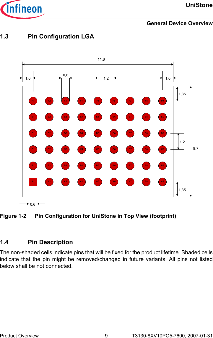
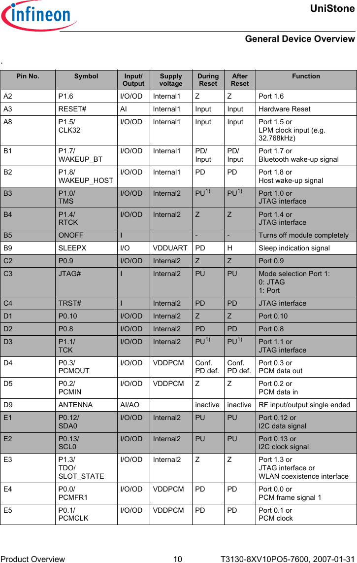
>
Trimble
>
642356X B1 User Manual
User Manual
Navigation menu
Upload a User Manual
Namespaces
Wiki Guide
HTML
PDF
Info
Views
User Manual
Discussion / Help
Navigation