Trimble 642356X-B1 Trimble R8 GNSS Receiver User Manual UniStone Product Overview
Trimble Navigation Ltd Trimble R8 GNSS Receiver UniStone Product Overview
Trimble >
User Manual

Never stop thinking.
Product Overview T3130-8XV10PO5-7600
Jan 2007
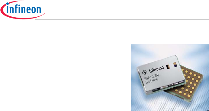
PBA 31308
Bluetooth QD ID: B012097/B012098
UniStone
BlueMoon Universal Platform

Edition 2007-01-31
Published by
Infineon Technologies AG
81726 Munich, Germany
© Infineon Technologies AG 2007.
All Rights Reserved.
Attention please!
The information herein is given to describe certain components and shall not be considered as warranted
characteristics.
Terms of delivery and rights to technical change reserved.
We hereby disclaim any and all warranties, including but not limited to warranties of non-infringement, regarding
circuits, descriptions and charts stated herein.
Infineon Technologies is an approved CECC manufacturer.
Information
For further information on technology, delivery terms and conditions and prices please contact your nearest
Infineon Technologies Office in Germany or our Infineon Technologies Representatives worldwide (see address
list).
Warnings
Due to technical requirements components may contain dangerous substances. For information on the types in
question please contact your nearest Infineon Technologies Office.
Infineon Technologies Components may only be used in life-support devices or systems with the express written
approval of Infineon Technologies, if a failure of such components can reasonably be expected to cause the failure
of that life-support device or system, or to affect the safety or effectiveness of that device or system. Life support
devices or systems are intended to be implanted in the human body, or to support and/or maintain and sustain
and/or protect human life. If they fail, it is reasonable to assume that the health of the user or other persons may
be endangered.

For questions on technology, delivery and prices, please contact the Infineon
Technologies Offices in Germany or the Infineon Technologies Companies and
Representatives worldwide: see our webpage at http://www.infineon.com
ABM®, AOP®, ARCOFI®, ARCOFI®-BA, ARCOFI®-SP, DigiTape®, EPIC®-1, EPIC®-S,
ELIC®, FALC®54, FALC®56, FALC®-E1, FALC®-LH, IDEC®, IOM®, IOM®-1, IOM®-2,
IPAT®-2, ISAC®-P, ISAC®-S, ISAC®-S TE, ISAC®-P TE, ITAC®, IWE®, MUSAC®-A,
OCTAT®-P, QUAT®-S, SICAT®, SICOFI®, SICOFI®-2, SICOFI®-4, SICOFI®-4µC,
SLICOFI® are registered trademarks of Infineon Technologies AG.
ACE™, ASM™, ASP™, POTSWIRE™, QuadFALC™, SCOUT™ are trademarks of
Infineon Technologies AG.
ARM, the ARM Powered logo, Thumb and StrongARM are registered trademarks of
ARM Limited. The ARM logo, AMBA, ARMulator, EmbeddedICE, ModulGen, Multi-ICE,
PrimeCell, ARM7TDMI, ARM7TDMI-S, ARM9TDMI, TDMI and STRONG are
trademarks of ARM Limited.
The Bluetooth® word mark is owned by the Bluetooth SIG, Inc. and any use of this mark
by Infineon Technologies AG is under license.
The BlueMoon® trade mark is owned by Infineon Technologies AG.

UniStone
Product Overview 4 T3130-8XV10PO5-7600, 2007-01-31
PBA 31308
Revision History: 2007-01-31 T3130-8XV10PO5-7600
Previous Version:
Section Subjects (major changes since last revision)

UniStone
Product Overview 5 T3130-8XV10PO5-7600, 2007-01-31
1 General Device Overview . . . . . . . . . . . . . . . . . . . . . . . . . . . . . . . . . . . . . 7
1.1 Features . . . . . . . . . . . . . . . . . . . . . . . . . . . . . . . . . . . . . . . . . . . . . . . . . . . . 7
1.2 Block Diagram . . . . . . . . . . . . . . . . . . . . . . . . . . . . . . . . . . . . . . . . . . . . . . . 8
1.3 Pin Configuration LGA . . . . . . . . . . . . . . . . . . . . . . . . . . . . . . . . . . . . . . . . . 9
1.4 Pin Description . . . . . . . . . . . . . . . . . . . . . . . . . . . . . . . . . . . . . . . . . . . . . . . 9
1.5 System Integration . . . . . . . . . . . . . . . . . . . . . . . . . . . . . . . . . . . . . . . . . . . 12
1.6 FW version . . . . . . . . . . . . . . . . . . . . . . . . . . . . . . . . . . . . . . . . . . . . . . . . . 13
2 Basic Operating Information . . . . . . . . . . . . . . . . . . . . . . . . . . . . . . . . . 14
2.1 Power Supply . . . . . . . . . . . . . . . . . . . . . . . . . . . . . . . . . . . . . . . . . . . . . . . 14
2.2 Clocking . . . . . . . . . . . . . . . . . . . . . . . . . . . . . . . . . . . . . . . . . . . . . . . . . . . 14
3 Interfaces . . . . . . . . . . . . . . . . . . . . . . . . . . . . . . . . . . . . . . . . . . . . . . . . . 15
3.1 HCI / UART Interface . . . . . . . . . . . . . . . . . . . . . . . . . . . . . . . . . . . . . . . . . 15
3.1.1 Supported Transport Layers . . . . . . . . . . . . . . . . . . . . . . . . . . . . . . . . . 15
3.1.2 UART . . . . . . . . . . . . . . . . . . . . . . . . . . . . . . . . . . . . . . . . . . . . . . . . . . . 15
3.1.2.1 Baud Rates . . . . . . . . . . . . . . . . . . . . . . . . . . . . . . . . . . . . . . . . . . . . 16
3.2 PCM Interface . . . . . . . . . . . . . . . . . . . . . . . . . . . . . . . . . . . . . . . . . . . . . . 17
3.2.1 Overview . . . . . . . . . . . . . . . . . . . . . . . . . . . . . . . . . . . . . . . . . . . . . . . . 18
3.3 WLAN Coexistence Interface . . . . . . . . . . . . . . . . . . . . . . . . . . . . . . . . . . . 19
4 General Device Capabilities . . . . . . . . . . . . . . . . . . . . . . . . . . . . . . . . . . 20
4.1 HCI+ and Bluetooth Device Data (BD_DATA) . . . . . . . . . . . . . . . . . . . . . . 20
4.2 Manufacturer Mode . . . . . . . . . . . . . . . . . . . . . . . . . . . . . . . . . . . . . . . . . . 20
4.3 Firmware ROM Patching . . . . . . . . . . . . . . . . . . . . . . . . . . . . . . . . . . . . . . 20
4.3.1 Patch Support . . . . . . . . . . . . . . . . . . . . . . . . . . . . . . . . . . . . . . . . . . . . 20
5 Bluetooth Capabilities . . . . . . . . . . . . . . . . . . . . . . . . . . . . . . . . . . . . . . . 22
5.1 Supported Features . . . . . . . . . . . . . . . . . . . . . . . . . . . . . . . . . . . . . . . . . . 22
5.2 UniStone Specifics and Extensions . . . . . . . . . . . . . . . . . . . . . . . . . . . . . . 22
5.2.1 During Connection . . . . . . . . . . . . . . . . . . . . . . . . . . . . . . . . . . . . . . . . . 22
5.2.1.1 Scatternet and Piconet Capabilities . . . . . . . . . . . . . . . . . . . . . . . . . . 22
5.2.1.2 Role Switch . . . . . . . . . . . . . . . . . . . . . . . . . . . . . . . . . . . . . . . . . . . . 22
5.2.1.3 Dynamic Polling Strategy . . . . . . . . . . . . . . . . . . . . . . . . . . . . . . . . . . 23
5.2.1.4 Adaptive Frequency Hopping (AFH) . . . . . . . . . . . . . . . . . . . . . . . . . 23
5.2.1.5 Channel Quality Driven Data Rate Change (CQDDR) . . . . . . . . . . . 23
5.2.2 Synchronous Links . . . . . . . . . . . . . . . . . . . . . . . . . . . . . . . . . . . . . . . . 23
5.2.2.1 Interface . . . . . . . . . . . . . . . . . . . . . . . . . . . . . . . . . . . . . . . . . . . . . . . 24
5.2.2.2 Voice Coding . . . . . . . . . . . . . . . . . . . . . . . . . . . . . . . . . . . . . . . . . . . 24
5.2.3 RSSI and Output Power Control . . . . . . . . . . . . . . . . . . . . . . . . . . . . . . 24
5.2.3.1 Received Signal Strength Indication (RSSI) . . . . . . . . . . . . . . . . . . . 24
5.2.3.2 Output Power Control . . . . . . . . . . . . . . . . . . . . . . . . . . . . . . . . . . . . 24
5.2.3.3 Ultra Low Transmit Power . . . . . . . . . . . . . . . . . . . . . . . . . . . . . . . . . 25
6 Electrical Characteristics . . . . . . . . . . . . . . . . . . . . . . . . . . . . . . . . . . . . 26

UniStone
Product Overview 6 T3130-8XV10PO5-7600, 2007-01-31
6.1 Absolute Maximum Ratings . . . . . . . . . . . . . . . . . . . . . . . . . . . . . . . . . . . . 26
6.2 Operating Conditions . . . . . . . . . . . . . . . . . . . . . . . . . . . . . . . . . . . . . . . . . 27
6.3 DC Characteristics . . . . . . . . . . . . . . . . . . . . . . . . . . . . . . . . . . . . . . . . . . . 28
6.3.1 Pad Driver and Input Stages . . . . . . . . . . . . . . . . . . . . . . . . . . . . . . . . . 28
6.3.2 Pull-ups and Pull-downs . . . . . . . . . . . . . . . . . . . . . . . . . . . . . . . . . . . . 31
6.3.3 Protection Circuits . . . . . . . . . . . . . . . . . . . . . . . . . . . . . . . . . . . . . . . . . 31
6.4 AC Characteristics . . . . . . . . . . . . . . . . . . . . . . . . . . . . . . . . . . . . . . . . . . . 33
6.4.1 Characteristics of 32.768 kHz Clock Signal . . . . . . . . . . . . . . . . . . . . . . 33
6.5 RF Part . . . . . . . . . . . . . . . . . . . . . . . . . . . . . . . . . . . . . . . . . . . . . . . . . . . 33
6.5.1 Characteristics RF Part . . . . . . . . . . . . . . . . . . . . . . . . . . . . . . . . . . . . . 33
6.5.1.1 Bluetooth Related Specifications . . . . . . . . . . . . . . . . . . . . . . . . . . . . 33
7 Package Information . . . . . . . . . . . . . . . . . . . . . . . . . . . . . . . . . . . . . . . . 38
7.1 Package marking . . . . . . . . . . . . . . . . . . . . . . . . . . . . . . . . . . . . . . . . . . . . 38
7.2 Production Package . . . . . . . . . . . . . . . . . . . . . . . . . . . . . . . . . . . . . . . . . . 38
7.2.1 Pin mark . . . . . . . . . . . . . . . . . . . . . . . . . . . . . . . . . . . . . . . . . . . . . . . . . 39
8 Acronyms & Abbreviations . . . . . . . . . . . . . . . . . . . . . . . . . . . . . . . . . . . 40
UniStone
General Device Overview
Product Overview 7 T3130-8XV10PO5-7600, 2007-01-31
1 General Device Overview
1.1 Features
General
• Complete Bluetooth 2.0 + EDR solution
• Ultra low power design in 0.13 µm CMOS
• Temperature range from -40°C to 85°C
• Integrates ARM7TDMI, RAM and patchable ROM
• On-module voltage regulators. External supply 2.9-4.1V
• On-module EEPROM with configureable data
• Reference clock included
• Low power clock from internal oscillator or external low power clock (e.g. 32.768 kHz)
• Dynamic low power mode switching
Interfaces
• 3.25 MBaud UART with transport layer detection (HCI UART, HCI Three-Wire UART)
• PCM/I2S interface for digital audio
• WLAN coexistence interface
• General purpose I/Os with interrupt capabilities. JTAG for boundary scan and debug
RF
• Transmit power programmable from -45 dBm to 4.5 dBm
• Transmit power typ. 2.5 dBm (default settings)
• Receiver sensitivity typ. -86 dBm
• Integrated antenna switch, balun and antenna filter
• Integrated LNA with excellent blocking and intermodulation performance
• No external components except antenna
• Digital demodulation for optimum sensitivity and co-/adjacent channel performance
Bluetooth
• Piconet with seven slaves. Scatternet with two slave roles while still being visible
• SCO and eSCO with hardware accelerated audio signal processing
• Power control and RSSI. Hold, Park and Sniff.
• Adaptive Frequency Hopping, Quality of Service, Channel Quality Driven Data Rate
• Bluetooth security features: Authentication, Pairing and Encryption
• Bluetooth test mode and Infineon’s active Bluetooth tester mode
UniStone
General Device Overview
Product Overview 8 T3130-8XV10PO5-7600, 2007-01-31
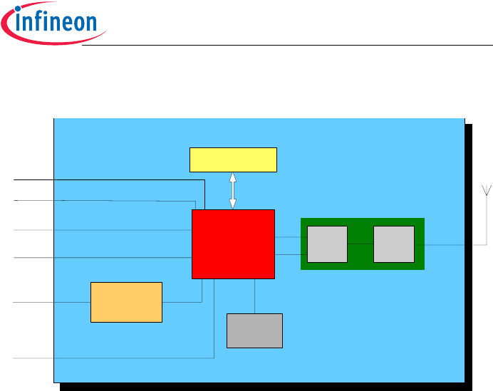
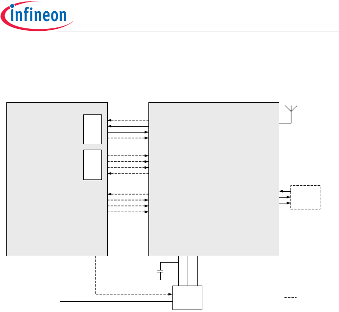
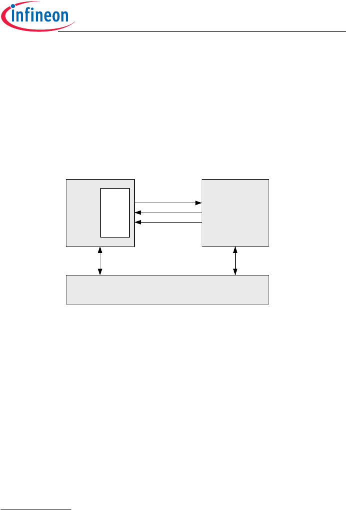
1.2 Block Diagram
Figure 1-1 Simplified block diagram of UniStone.
UniStone
PMB8753
BlueMoon
UniCellular
EEPROM
Voltage
Regulator
Crystal
26 MHz
Balun Filter
I
2
C
V
supply
Low Power Clock
(Optional)
32.768 kHz
PCM1
UART - HCI
VDD_UART
VDD_PCM
UniStone
General Device Overview
Product Overview 9 T3130-8XV10PO5-7600, 2007-01-31
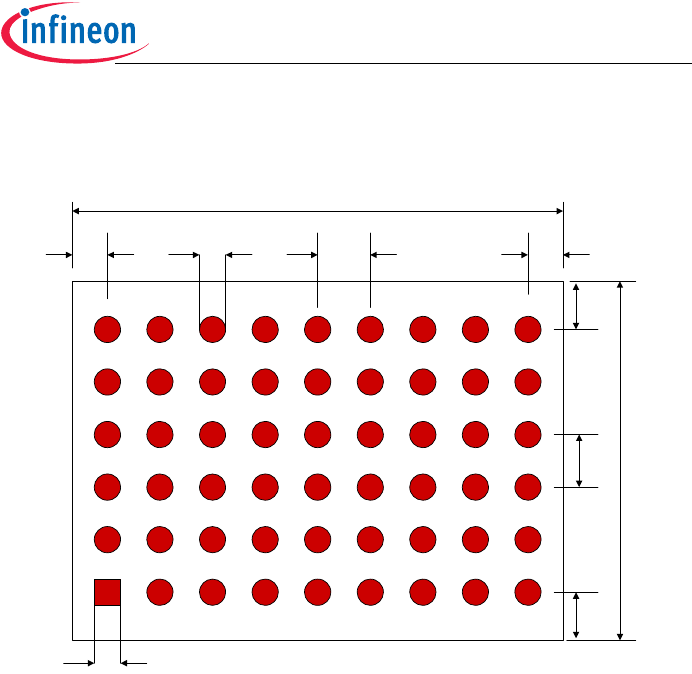
1.3 Pin Configuration LGA
Figure 1-2 Pin Configuration for UniStone in Top View (footprint)
1.4 Pin Description
The non-shaded cells indicate pins that will be fixed for the product lifetime. Shaded cells
indicate that the pin might be removed/changed in future variants. All pins not listed
below shall be not connected.
0,6
A2 A3 A4 A5 A6 A7 A8 A9
B1 B2 B3 B4 B5 B6 B7 B8 B9
C1 C2 C3 C4 C5 C6 C7 C8 C9
D1 D2 D3 D4 D5 D6 D7 D8 D9
E1 E2 E3 E4 E5 E6 E7 E8 E9
F1 F2 F3 F4 F5 F6 F7 F8 F9
A1
1,2 1,01,0 0,6
1,2
1,35
1,35
11,6
8,
7

UniStone
General Device Overview
Product Overview 10 T3130-8XV10PO5-7600, 2007-01-31
.
Pin No. Symbol Input/
Output
Supply
voltage
During
Reset
After
Reset
Function
A2 P1.6 I/O/OD Internal1 Z Z Port 1.6
A3 RESET# AI Internal1 Input Input Hardware Reset
A8 P1.5/
CLK32
I/O/OD Internal1 Input Input Port 1.5 or
LPM clock input (e.g.
32.768kHz)
B1 P1.7/
WAKEUP_BT
I/O/OD Internal1 PD/
Input
PD/
Input
Port 1.7 or
Bluetooth wake-up signal
B2 P1.8/
WAKEUP_HOST
I/O/OD Internal1 PD PD Port 1.8 or
Host wake-up signal
B3 P1.0/
TMS
I/O/OD Internal2 PU1) PU1) Port 1.0 or
JTAG interface
B4 P1.4/
RTCK
I/O/OD Internal2 Z Z Port 1.4 or
JTAG interface
B5 ONOFF I - - Turns off module completely
B9 SLEEPX I/O VDDUART PD H Sleep indication signal
C2 P0.9 I/O/OD Internal2 Z Z Port 0.9
C3 JTAG# IInternal2 PU PU Mode selection Port 1:
0: JTAG
1: Port
C4 TRST# IInternal2 PD PD JTAG interface
D1 P0.10 I/O/OD Internal2 Z Z Port 0.10
D2 P0.8 I/O/OD Internal2 PD PD Port 0.8
D3 P1.1/
TCK
I/O/OD Internal2 PU1) PU1) Port 1.1 or
JTAG interface
D4 P0.3/
PCMOUT
I/O/OD VDDPCM Conf.
PD def.
Conf.
PD def.
Port 0.3 or
PCM data out
D5 P0.2/
PCMIN
I/O/OD VDDPCM Z Z Port 0.2 or
PCM data in
D9 ANTENNA AI/AO inactive inactive RF input/output single ended
E1 P0.12/
SDA0
I/O/OD Internal2 PU PU Port 0.12 or
I2C data signal
E2 P0.13/
SCL0
I/O/OD Internal2 PU PU Port 0.13 or
I2C clock signal
E3 P1.3/
TDO/
SLOT_STATE
I/O/OD Internal2 Z Z Port 1.3 or
JTAG interface or
WLAN coexistence interface
E4 P0.0/
PCMFR1
I/O/OD VDDPCM PD PD Port 0.0 or
PCM frame signal 1
E5 P0.1/
PCMCLK
I/O/OD VDDPCM PD PD Port 0.1 or
PCM clock
UniStone
General Device Overview
Product Overview 11 T3130-8XV10PO5-7600, 2007-01-31
1) Fixed pull-up/pull-down if JTAG interface is selected, not affected by any chip reset.
If JTAG interface is not selected the port is tristate.
Descriptions of acronyms used in the pin list:
E6 P0.5/
UARTRXD
I/O/OD VDDUART Z Z Port 0.5 or
UART receive data
F2 P1.2/
TDI/
RF_ACTIVE
I/O/OD Internal2 PU1) PU1) Port 1.2 or
JTAG interface or
WLAN coexistence interface
F3 P0.11/
TX_CONF
I/O/OD Internal2 Z Z Port 0.11or
WLAN coexistence interface
F4 P0.14/
TX_CONF
I/O VDDUART Z Z Port 0.14 or
WLAN coexistence interface
F5 P0.7/
UARTCTS
I/O/OD VDDUART Z Z Port 0.7 or
UART CTS flow control
F7 P0.4/
UARTTXD
I/O/OD VDDUART PU PU Port 0.4 or
UART transmit data
F8 P0.6/
UARTRTS
I/O/OD VDDUART PU PU Port 0.6 or
UART RTS flow control
A4, A5, A6 VSUPPLY SI - - Power supply
C1 VREG SO - - Regulated Power supply
F6 VDDUART SI - - UART interface Power supply
C5 VDDPCM SI - - PCM interface Power supply
A1, A7, A9, C8,
C9, D7, D8, E8,
E9, F1, F9
VSS - - Ground
Acronym Description
I Input
O Output
OD Output with open drain capability
Z Tristate
PU Pull-up
PD Pull-down
A Analog (e.g. AI means analog input)
S Supply (e.g. SO means supply output)
Pin No. Symbol Input/
Output
Supply
voltage
During
Reset
After
Reset
Function
UniStone
General Device Overview
Product Overview 12 T3130-8XV10PO5-7600, 2007-01-31
1.5 System Integration
UniStone is optimized for a low bill of material (BOM) and a small PCB size. Figure 1-3
shows a typical application example.
The UART interface is used for Bluetooth HCI communication between the host and
UniStone. When the HCI UART transport layer is used, four interface lines are needed:
two for data (UARTTXD and UARTRXD) and two for hardware flow control (UARTRTS
and UARTCTS). When the HCI Three-Wire UART transport layer is used the hardware
flow control lines are optional. In addition to the standard Bluetooth HCI commands,
UniStone supports a set of Infineon specific commands called HCI+.
Digital audio can either be sent over the HCI interface or over the dedicated PCM/I2S
interface. The PCM/I2S interface is highly configurable.
Low power mode control of UniStone and the host can be implemented in different ways,
either using the dedicated WAKEUP_HOST and WAKEUP_BT signals or using
signaling over the HCI interface. The host can reset UniStone via the RESET# signal.
A low power clock can be connected to CLK32 or generated internally by a low power
oscillator. Power is supplied to a single VSUPPLY input from which internal regulators
can generate all required voltages. The UART and the PCM interfaces have separate
supply voltages so that they can comply with host signaling.
Figure 1-3 Example Bluetooth System
UniStone
UARTRTS
UARTTXD
UARTRXD
UARTCTS
PCMCLK
PCMFR1
PCMIN
PCMOUT
WAKEUP_HOST
WAKEUP_BT
RESET#
CLK32
HOST
UARTPCM / I2S
ANTENNA
RF_ACTIVE
TX_CONF
SLOT_STATE
WLAN
Subsystem
VDDSUP
Power
Supply Optional
VDDUART
VDDPCM

UniStone
General Device Overview
Product Overview 13 T3130-8XV10PO5-7600, 2007-01-31
If a WLAN subsystem is collocated with UniStone the WLAN coexistence interface
should be used to enhance Bluetooth and WLAN performance. To coexist with external
WLAN devices UniStone supports adaptive frequency hopping.
1.6 FW version
UniStone is available in different versions. Please check corresponding release
documents for latest information.

UniStone
Basic Operating Information
Product Overview 14 T3130-8XV10PO5-7600, 2007-01-31
2 Basic Operating Information
2.1 Power Supply
BlueMoon UniCellular is supplied from a single supply voltage VSUPPLY. This supply
voltage must always be present. The Bluemoon UniCellular chip is supplied from an
internally generated 2.5 V supply voltage. This voltage can be accessed from the VREG
pin. This voltage may not be used for supplying other components in the host system but
can be used for referencing the host interfaces.
The PCM interface and the UART interface are supplied with dedicated, independent,
reference levels via the VDDPCM and VDDUART pins. All other digital I/O pins are
supplied internally by either 2.5 V (Internal2) or 1.5 V(Internal1). Section 1.4 provides a
mapping between pins and supply voltages.
The I/O power domains (VDDPCM and VDDUART) are completely separated from the
other power domains and can stay present also in low power modes.
2.2 Clocking
BlueMoon UniCellular has one clock input CLK32 that is optional. If used this 32.768 kHz
clock must always be present to assist BlueMoon UniCellular to keep the time in low
power modes.
The low power clock can be generated internally by the crystal oscillator and/or the low
power oscillator or provided externally.
UniStone
Interfaces
Product Overview 15 T3130-8XV10PO5-7600, 2007-01-31
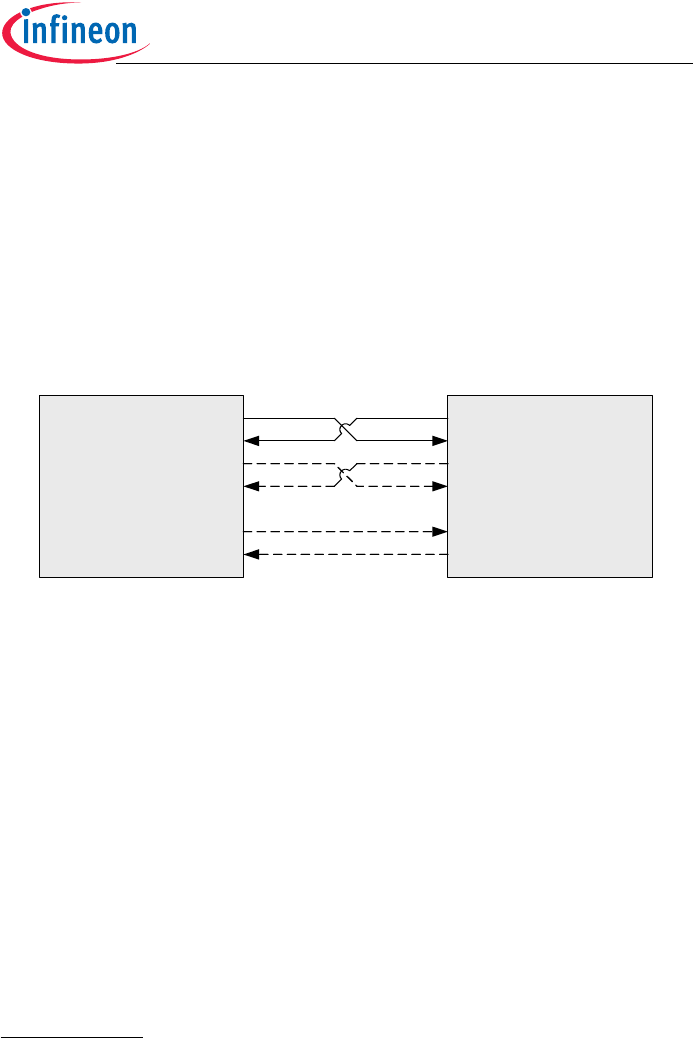
3 Interfaces
3.1 HCI / UART Interface
The HCI/UART interface is the main communication interface between the host and
UniStone. The standard HCI commands are supported together with an Infineon specific
set of commands called HCI+.
The interface consists of four UART signals and two wake-up signals as shown in
Figure 3-1. Depending on which HCI transport layer that is used, some or all of the
signals are needed.
3.1.1 Supported Transport Layers
UniStone supports the HCI Three-Wire UART transport layer and two derivatives of the
HCI UART transport layer (HCI UART-4W and HCI-UART-6W) where the only difference
is how low power modes are handled. UniStone automatically detects which transport
layer that is used by the host.
3.1.2 UART
The on-chip UART (Universal Asynchronous Receiver and Transmitter) is compatible
with standard UARTs and is optimized for Bluetooth communication. Hardware support
for SLIP1) framing and 16-bit CRC calculation enhances performance with the HCI
Three-Wire UART transport layer. A separate supply voltage, VDDUART, makes it easy
to connect the UART interface to any system.
1) See http://www.ietf.org/rfc/rfc1055.txt for information about SLIP.
Figure 3-1 HCI/UART Interface
UARTTXD
UARTRXD
UARTRTS
UARTCTS
WAKEUP_BT
WAKEUP_HOST
UARTTXD
UARTRXD
UARTRTS
UARTCTS
WAKEUP_BT
WAKEUP_HOST
Host UniStone
UniStone
Interfaces
Product Overview 16 T3130-8XV10PO5-7600, 2007-01-31
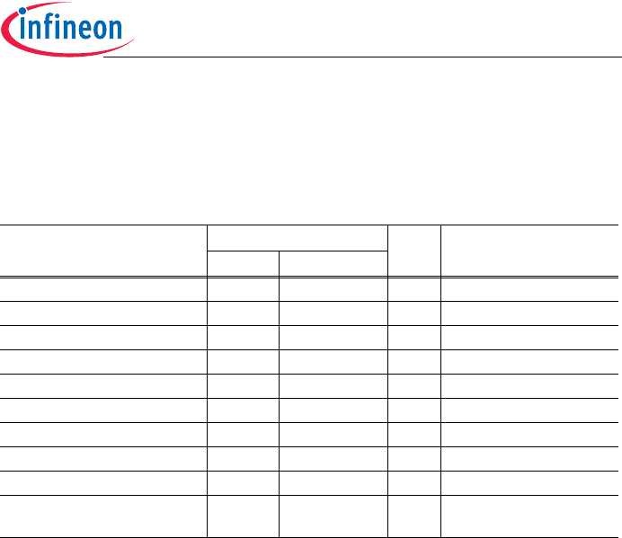
3.1.2.1 Baud Rates
The supported baud rates are listed in Table 3-1 together with the small deviation error
that results from the internal clock generation. The default baud rate is 115200 Baud.
Table 3-1 UART Baud Rates
Wanted Baud Rate Real Baud Rate Deviation Error (%)
9600 9615 0.16
19200 19230 0.16
38400 38461 0.16
57600 57522 -0.14
115200 115044 -0.14
230400 230088 -0.14
460800 464285 0.76
921600 928571 0.76
1843200 1857142 0.76
3250000 3250000 0

UniStone
Interfaces
Product Overview 17 T3130-8XV10PO5-7600, 2007-01-31
3.2 PCM Interface
The PCM interface is used to exchange synchronous data (usually audio) between
UniStone and the host as well as to connect e.g. an external audio codec or an external
DSP to UniStone. It can be configured as an industry standard PCM interface supporting
long and short frame synchronization, as an I2S interface1) or as an IOM-2 interface in
terminal mode with reduced capabilities.
The main features of the PCM interface are:
• Two bidirectional PCM channels
• Separate supply voltage (VDDPCM) for easy interfacing to other systems
• Support for all sample types defined in the Bluetooth specification
(Up to 16-bit linear samples and 8-bit A-law/µ-law compressed samples)2)
• 8x32-bit FIFOs for each channel
• Programmable frame length
• Programmable frame signal length
• Programmable channel start positions
• Programmable idle level on PCMOUT
• Programmable low-power/inactive levels on all PCM pins
• Data word LSB justified or MSB justified with respect to frame signal
• Clock master/slave mode
• Frame master/slave mode
• Fractional divider for PCM clock generation
1) Does not support variable word length. Hardware supports 16 or 24 bits. Current firmware supports 16 bits.
2) The hardware supports data word lengths of up to 24 bits.
UniStone
Interfaces
Product Overview 18 T3130-8XV10PO5-7600, 2007-01-31
3.2.1 Overview
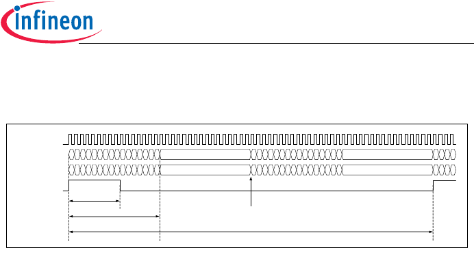
The PCM interface consists of four signals as shown in Figure 3-2 below
The clock signal PCMCLK is the timing base for the other signals in the PCM interface.
In clock master mode, UniStone generates PCMCLK from the internal system clock
using a fractional divider. In clock slave mode PCMCLK is an input to UniStone and has
to be supplied by an external source. The maximum PCMCLK frequency (in both modes)
is 1/8 of the internal system clock frequency.
The PCM interface supports up to two bidirectional channels. Data is transmitted on
PCMOUT and received on PCMIN, always with the most significant bit first. The
hardware supports a Data Word Length of 16 or 24 bits. The firmware always uses 16
bits since that is the maximum audio sample size (linear samples can be up to 16 bits,
A-law or µ-law compressed samples are always 8 bits).
The samples are organized in frames such that each frame contains one sample in each
direction of each active channel. The frame rate (i.e. sample rate) is controlled by the
PCMCLK frequency and the programmable Frame Length. In the firmware the sample
rate has been fixed to 8 kHz. This means that the PCMCLK frequency can be calculated
from Frame Length and does not have to be specified.
Channel 1 has a frame signal (PCMFR1) that indicates where in the frame the channel
starts. The Frame Signal Length is programmable.
In frame master mode, UniStone generates PCMFR1. In frame slave mode the signal
PCMFR1 is an input to UniStone and has to be supplied externally.
Figure 3-2 PCM Signals Overview
PCMCLK
PCMIN
PCMFR1
PCMOUT M
S
B
1
4
1
3
1
2
1
1
1
0987654321
L
S
B
M
S
B
1
4
1
3
1
2
1
1
1
0987654321
L
S
B
M
S
B
1
4
1
3
1
2
1
1
1
0987654321
L
S
B
M
S
B
1
4
1
3
1
2
1
1
1
0987654321
L
S
B
M
S
B
1
4
1
3
1
2
M
S
B
1
4
1
3
1
2
IDLE IDLE
Don’t Care Don’t Care
Channel 2 Start PositionFrame Signal Length
Data Word Length
Frame Length
UniStone
Interfaces
Product Overview 19 T3130-8XV10PO5-7600, 2007-01-31
3.3 WLAN Coexistence Interface
UniStone has a WLAN coexistence interface that is based on the IEEE 802.15.2 Packet
Traffic Arbitration (PTA) scheme1). The interface prevents interference between
collocated WLAN and Bluetooth devices by not letting the two devices transmit and/or
receive at the same time. WLAN packets and Bluetooth packets are assigned priorities,
and a control unit decides on a per-packet basis which of the devices that should be
allowed to operate.
The interface uses three wires as shown in Figure 3-3.
1) “802.15.2: Coexistence of Wireless Personal Area Networks with other Wireless Devices Operating in
Unlicensed Frequency Bands”, IEEE, 28 August 2003
Figure 3-3 WLAN Coexistence Interface
TX_CONF
SLOT_STATE
RF_ACTIVE
Control
Unit
Host
Host UniStone

UniStone
General Device Capabilities
Product Overview 20 T3130-8XV10PO5-7600, 2007-01-31
4 General Device Capabilities
4.1 HCI+ and Bluetooth Device Data (BD_DATA)
In addition to the standard Bluetooth HCI commands and events, UniStone supports a
set of Infineon specific commands and events called HCI+. All Infineon specific features
are accessed using HCI+.
All configuration information that is critical for correct operation of UniStone is called
Bluetooth Device Data (BD_DATA). This data is stored in the module’s EEPROM and is
initialized during module manufacturing. BD_DATA can be read and written with the
HCI+ commands Infineon_Read_BD_Data and Infineon_Write_BD_Data.
Important Note: Each UniStone module is delivered with BD_DATA containing a unique
Bluetooth device address aswell as configuration parameters for the device. This
information should not be changed unless expressly allowed to do so. Please consult
manufacturer in uncertain cases.
4.2 Manufacturer Mode
HCI+ commands that modify critical information are not available during normal
operation. To access these commands the host must first tell UniStone to enter
manufacturer mode with the Infineon_Manufacturer_Mode command.
Operations that are only allowed in manufacturer mode are for example:
• Changing the Baud rate with Infineon_Set_UART_Baudrate.
• Switching to the built-in boot loader with Infineon_Switch_To_Loader. The loader is
primarily used for firmware evaluation and is not described in this document.
• Accessing Bluetooth Device Data (BD_DATA) with any of the following commands:
Infineon_Write_BD_Data, Infineon_Read_BD_Data,
Infineon_Write_Ext_EEPROM_Data, Infineon_Read_Ext_EEPROM_Data.
• Accessing internal memory and registers with
Infineon_Memory_Write and Infineon_Memory_Read.
It is necessary to leave manufacturer mode before start of normal operation. Leaving
manufacturer mode is done with the Infineon_Manufacturer_Mode command.
4.3 Firmware ROM Patching
4.3.1 Patch Support
UniStone contains dedicated hardware that makes it possible to apply patches to any
code and data in the firmware ROM. The hardware is capable of replacing up to 32
blocks of 16 bytes each with new content. In addition to this, a 12 kByte area of the
firmware RAM has been reserved for patches. This area can be filled with any

UniStone
General Device Capabilities
Product Overview 21 T3130-8XV10PO5-7600, 2007-01-31
combination of code and data. Please consult manufacturer for latest information of
available patches.

UniStone
Bluetooth Capabilities
Product Overview 22 T3130-8XV10PO5-7600, 2007-01-31
5 Bluetooth Capabilities
5.1 Supported Features
UniStone supports all features in the Bluetooth 2.0 + EDR specification, including:
• Enhanced Data Rate up to 3 Mbit/s
• Adaptive Frequency Hopping (AFH)
• All packet types
• All LMP features
• Authentication, Pairing and Encryption
• Quality of Service
• Channel Quality Driven Data Rate change
• Sniff, Hold and Park
•Role Switch
• RSSI and Power Control
• Power class 1, 2 and 3
• 7 point-to-multipoint connections
• Scatternet with two slave roles while still being visible
• 2 synchronous links (SCO/eSCO)
•A-law, µ-law, CVSD and transparent synchronous data
• Dual SCO/eSCO channels in scatternet
5.2 UniStone Specifics and Extensions
5.2.1 During Connection
5.2.1.1 Scatternet and Piconet Capabilities
UniStone supports point-to-multipoint and scatternet scenarios:
• Up to 7 links
• Up to 2 simultaneous slave roles
• Always capable of responding to inquiry and remote name request
• Always capable of Inquiry
5.2.1.2 Role Switch
Only one role switch can be performed at a time. If a role switch request is pending, other
role switch requests on the same or other links are rejected. If a role switch fails,
UniStone will automatically try again a maximum of three times. Encryption (if present)
is stopped in the old piconet before a role switch is performed and re-enabled when the
role switch has succeeded or failed. If the physical link is in Sniff Mode, Hold Mode or

UniStone
Bluetooth Capabilities
Product Overview 23 T3130-8XV10PO5-7600, 2007-01-31
Park State, or has any synchronous logical transports, a role switch will not be
performed.
5.2.1.3 Dynamic Polling Strategy
In addition to the regular polling scheme, UniStone dynamically assigns unused slots to
links where data is exchanged. This adapts very well to bursty traffic and improves
throughput and latency on the links.
5.2.1.4 Adaptive Frequency Hopping (AFH)
UniStone supports adaptive frequency hopping according to the Bluetooth 2.0 + EDR
specification. AFH switch and channel classification are supported both as master and
slave. Channel classification from the host is also supported.
A number of HCI+ commands and events are available to provide information about AFH
operation. The commands Infineon_Enable_AFH_Info_Sending and Infineon_Disable_
AFH_Info_Sending turn on and off the Infineon AFH Info events that provide detailed
information about channel classification, channel maps, interferers, etc.
If enabled by the Infineon_Enable_Infineon_Events command, the Infineon AFH
Extraordinary RSSI event informs the host whenever extraordinary RSSI measurements
in unused slots have been started. This is done when the number of known good
channels has decreased below a critical limit and periodically after a defined time.
The Infineon_Set_AFH_Measurement_Period command can be used to configure the
duration of the AFH measurement period.
5.2.1.5 Channel Quality Driven Data Rate Change (CQDDR)
UniStone supports channel quality driven data rate change according to the Bluetooth
2.0 + EDR specification. A device that receives an LMP_preferred_rate message is not
required to follow all recommendations. UniStone normally at least follows the
recommendation whether to use forward error correction (FEC) or not. If possible,
recommendations about packet size and modulation scheme will be taken into account.
When UniStone sends an LMP_preferred_rate to another device the proposal always
includes preferences for all parameters.
The HCI+ commands Infineon_Enable_CQDDR_Info_Sending and Infineon_Disable_
CQDDR_Info_Sending turn on and off sending of the Infineon CQDDR Info event. This
event provides information to the host every time a new CQDDR proposal is sent to a
remote device.
5.2.2 Synchronous Links
UniStone supports up to two simultaneous synchronous links (SCO/eSCO).
UniStone
Bluetooth Capabilities
Product Overview 24 T3130-8XV10PO5-7600, 2007-01-31
5.2.2.1 Interface
The interface for synchronous data is either the HCI transport layer or the dedicated
PCM/I2S interface. The choice of interface for a synchronous connection is done with
the HCI+ command Infineon_Config_Synchronous_Interface and must be done before
the connection is established. The default interface is configurable via the bit Default_
SCO_interface in the BD_DATA parameter BB_Conf.
All details about the PCM/I2S interface are described in Section 3.2.
5.2.2.2 Voice Coding
Table 5-1 shows the supported values of the Bluetooth parameter Voice_Settings.
UniStone supports transcoding between any combination of linear, µ-law and A-law. If
the air coding format is “Transparent Data” and the synchronous interface is the
transport layer, the input coding is ignored. If transparent data is sent through the PCM/
I2S interface, the input coding determines if 8-bit or 16-bit samples are used.
Transparent Data is the only setting for which data rates other than 64 kbit/s can be used.
5.2.3 RSSI and Output Power Control
5.2.3.1 Received Signal Strength Indication (RSSI)
UniStone supports received signal strength measurements and uses LMP signaling to
keep the output power of a remote device within the golden receive power range. The
range is set with the BD_DATA parameters RSSI_Min and RSSI_Max.
5.2.3.2 Output Power Control
UniStone supports power control according to the Bluetooth 2.0 + EDR specification.
• The output power can be controlled in 4 steps when an external power amplifier is
present.
• The output power can be controlled in 3 or 4 steps (configurable) with internal power
settings. In this case no power amplifier is present; therefore UniStone can work as a
class 1, 2 or 3 device depending on the settings.
Table 5-1 Supported Voice Settings
Parameter Supported Values
Input Coding Linear (PCM/I2S only), µ-law, A-law
Input Data Format 2’s complement
Input Sample Size 16-bit (only relevant for linear input coding)
Air Coding Format CVSD, µ-law, A-law, Transparent Data

UniStone
Bluetooth Capabilities
Product Overview 25 T3130-8XV10PO5-7600, 2007-01-31
• Fine tuning can be used on the power steps.
The following BD_DATA parameters are used for configuration:
RF_Psel_D, RF_Psel_Conf, RF_Conf, TX_Power_Ref#.
5.2.3.3 Ultra Low Transmit Power
For high security devices the output power can be reduced to a value that reduces the
communication range to a few inches. This mode is enabled with the HCI+ command
Infineon_TX_Power_Config.
UniStone
Electrical Characteristics
Product Overview 26 T3130-8XV10PO5-7600, 2007-01-31
6 Electrical Characteristics
6.1 Absolute Maximum Ratings
Note: Stresses above those listed here are likely to cause permanent damage to
the device. Exposure to absolute maximum rating conditions for extended
periods may affect device reliability.
Maximum ratings are absolute ratings; exceeding only one of these values
may cause irreversible damage to the integrated circuit.
Maximum ratings are not operating conditions.
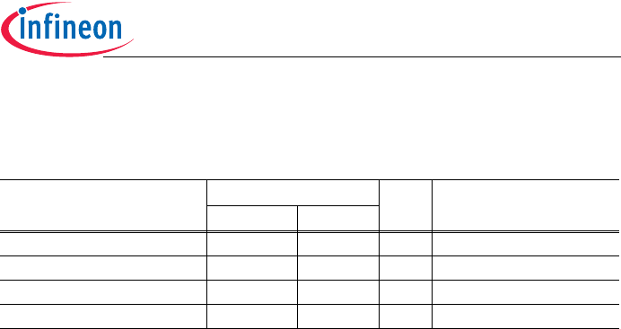
Table 6-1 Absolute Maximum Ratings
Parameter Limit Values Unit Notes
Min Max
Storage temperature -40 125 oC-
VSUPPLY supply voltage -0.3 6.0 V -
VDDUART supply voltage -0.9 4.0 V -
VDDPCM supply voltage -0.9 4.0 V -
VREG -0.3 4.0 V VSUPPLY > 4 V
VREG -0.3 VSUPPLY V VSUPPLY < 4 V
ONOFF -0.3 VSUPPLY+0.3 V -
Input voltage range -0.9 4.0 V -
Output voltage range -0.9 4.0 V -
ESD 1.0 kV According to MIL-
STD883D method 3015.7
UniStone
Electrical Characteristics
Product Overview 27 T3130-8XV10PO5-7600, 2007-01-31
6.2 Operating Conditions
Table 6-2 Operating Conditions
Parameter Limit Values Unit Notes
Min Max
Operating temperature -40 85 oC-
Main supply voltage (Vsupply) 2.9 4.1 V
VDDUART 1.35 3.6 V
VDDPCM 1.35 3.6 V
UniStone
Electrical Characteristics
Product Overview 28 T3130-8XV10PO5-7600, 2007-01-31
6.3 DC Characteristics
6.3.1 Pad Driver and Input Stages
Table 6-3 Internal1 (1.5 V) supplied Pins (see Chapter 1.4)
Table 6-4 Internal2 (2.5 V) supplied Pins (see Chapter 1.4)
Parameter Condition Limit Values Unit
Min Typ Max
Input low voltage - -0.3 0.27 V
Input high voltage - 1.15 3.6 V
Output low voltage IOL=1mA 0.25 V
Output high voltage IOH=-1mA, 1.1 V
Continuous Load1)
1) The totaled continuous load for all Internal1 supplied pins shall not exceed 2mA at the same time
1mA
Pin Capacitance 10 pF
Magnitude Pin
Leakage
input and output
drivers disabled
0.01 1 µA
Parameter Condition Limit Values Unit
Min Typ Max
Input low voltage - -0.3 0.45 V
Input high voltage -P0.10 1.93 2.8 V
-Other pins 1.93 3.6 V
Output low voltage IOL=5mA 0.25 V
Output low voltage IOL=2mA 0.15 V
Output high voltage IOH=-5mA, 2.0 V
Output high voltage IOH=-2mA, 2.1 V
Continuous Load1)
1) The totaled continuous load for all Internal2 supplied pins shall not exceed 35mA at the same time
5mA
Pin Capacitance 10 pF
Magnitude Pin
Leakage
input and output
drivers disabled
0.01 1 µA
UniStone
Electrical Characteristics
Product Overview 29 T3130-8XV10PO5-7600, 2007-01-31
Table 6-5 VDDUART supplied Pins (see Chapter 1.4)
Parameter Condition Limit Values Unit
Min Typ Max
Input low voltage -0.3 0.2*VDDUART V
Input high voltage P0.5/UARTRXD 0.7*VDDUART VDDUART+0.3 V
-Other pins 0.7*VDDUART 3.6 V
Output low voltage IOL=5mA
VDDUART=2.5V
0.25 V
Output low voltage IOL=2mA
VDDUART=2.5V
0.15 V
Output high voltage IOH=-5mA,
VDDUART=2.5V
VDDUART-0.25 V
Output high voltage IOH=-2mA,
VDDUART=2.5V
VDDUART-0.15 V
Continuous Load1)
1) The totaled continuous load for all VDDUART supplied pins shall not exceed 35mA at the same time
5mA
Pin Capacitance 10 pF
Magnitude Pin
Leakage
input and output
drivers disabled
0.01 1 µA
UniStone
Electrical Characteristics
Product Overview 30 T3130-8XV10PO5-7600, 2007-01-31
Table 6-6 VDDPCM supplied Pins (see Chapter 1.4)
Table 6-7 ONOFF PIN (see Chapter 1.4)
Parameter Condition Limit Values Unit
Min Typ Max
Input low voltage -0.3 0.2*VDDPCM V
Input high voltage 0.7*VDDPCM 3.6 V
Output low voltage IOL=5mA
VDDPCM=2.5V
0.25 V
Output low voltage IOL=2mA
VDDPCM=2.5V
0.15 V
Output high voltage IOH=-5mA,
VDDPCM=2.5V
VDDPCM-0.25 V
Output high voltage IOH=-2mA,
VDDPCM=2.5V
VDDPCM-0.15 V
Continuous Load1)
1) The totaled continuous load for all VDDPCM supplied pins shall not exceed 35mA at the same time
5mA
Pin Capacitance 10 pF
Magnitude Pin
Leakage
input and output
drivers disabled
0.01 1 µA
Parameter Condition Limit Values Unit
Min Typ Max
Input low voltage 0.7 V
Input high voltage 1.7 VSUPPLY V
Input current ONOFF=0V -1 0.01 1 µA

UniStone
Electrical Characteristics
Product Overview 31 T3130-8XV10PO5-7600, 2007-01-31
6.3.2 Pull-ups and Pull-downs
6.3.3 Protection Circuits
All pins have an inverse protection diode against VSS.
P0.10 has an inverse diode against Internal2.
P0.5/UARTRXD has an inverse diode against VDDUART.
All other pins have no diode against their supply.
Table 6-8 Pull-up and pull-down currents
Pin Pull Up Current Pull Down Current Unit Conditions
Min Typ Max Min Typ Max
P0.12/SDA0,
P0.13/SCL0
260 740 1300 N/A N/A N/A µA Pull-up current
measured with
pin voltage = 0V
Pull-down current
measured with
pin voltage =
supply voltage
Min measured at
125°C with
supply = 1.35V
Typ measured at
27°C with
supply = 2.5V
Max measured at
-40°C with
supply = 3.63V
TRST#, JTAG#,
P0.0/PCMFR1,
P0.1/PCMCLK,
P0.2/PCMIN,
P0.3/PCMOUT
22 130 350 23 150 380 µA
P0.4/UARTTXD,
P0.5/UARTRXD,
P0.6/UARTRTS,
P0.7/UARTCTS,
P0.10/PSEL1,
P0.8/PAON,
P0.9/PSEL0,
P0.11/RXON,
P0.14/TX_CONF,
P0.15/SLEEPX
4.2 24 68 3.0 20 55 µA
P1.0/TMS,
P1.1/TCK,
P1.2/TDI,
P1.3/TDO,
P1.4/RTCK,
P1.5/CLK32,
P1.6,
P1.7/WAKEUP_BT,
P1.8/WAKEUP_HOST,
1.1 6.0 17 0.75 5.0 14 µA
UniStone
Electrical Characteristics
Product Overview 32 T3130-8XV10PO5-7600, 2007-01-31
System Power Consumption
Table 6-9 Current Consumption In Different Operating Modes
This table shows the Vsupply current consumption. All I/O current is neglected since they
depend mainly on the external load.
T=25°C, Output Power=0dBm,
Parameters Min Typ Max Unit Comment
Ultra Low Power Mode 170 µA
Page & Inquiry Scan (1.28s) 1.1 mA
Sniff (1.28s) 0.35 mA
ACL (Transmit DH1) 38 mA Basic Rate, 179.2 kb/s1)
1) Figure indicates maximum possible data rate with this packet type
ACL (Receive DH1) 35 mA Basic Rate, 179.2 kb/s
ACL (Transmit 2-DH1) 40 mA Enhanced Data Rate, 358.4 kb/
s1)
ACL (Receive 2-DH1) 37 mA Enhanced Data Rate, 358.4 kb/
s1)
ACL (Transmit 3-DH1) 40 mA Enhanced Data Rate, 544.0 kb/
s1)
ACL (Receive 3-DH1) 37 mA Enhanced Data Rate, 544.0 kb/
s1)
SCO (HV3) 19 mA
eSCO (Symmetric 64 kb/s, EV3) 20 mA
eSCO (Symmetric 64 kb/s, 2-EV3) 13 mA Enhanced Data Rate
eSCO (Symmetric 64 kb/s, 3-EV3) 11 mA Enhanced Data Rate
eSCO (Symmetric 64 kb/s, EV5) 14 mA
eSCO (Symmetric 64 kb/s, 2-EV5) 10 mA Enhanced Data Rate
eSCO (Symmetric 64 kb/s, 3-EV5) 8.7 mA Enhanced Data Rate
Table 6-10 Max. Load at the Different Supply Voltages
I/O currents are not included since they depend mainly on external loads.
Parameters Min Typ Max Unit Comment
Vsupply 100 mA peak current
UniStone
Electrical Characteristics
Product Overview 33 T3130-8XV10PO5-7600, 2007-01-31
6.4 AC Characteristics
6.4.1 Characteristics of 32.768 kHz Clock Signal
The 32.768 kHz clock signal applied to CLK32 must be a rectangular waveform with a
duty cycle of between 10-90%. The frequency accuracy must be better than 250 ppm.
The rise and fall time of the signal must be less than 10 µs.
6.5 RF Part
6.5.1 Characteristics RF Part
The characteristics involve the spread of values to be within the specific temperature
range. Typical characteristics are the median of the production.
All values refers to Infineon reference design. All values will be updated after verification/
Characterisation.
6.5.1.1 Bluetooth Related Specifications
Table 6-11 BDR - Transmitter Part
Parameters Min Typ Max Unit Conditions
Output power (high gain) 0.5 2.5 4.5 dBm Default settings
Output power (highest gain) 4.5 dBm Maximum settings
Power control step size 468dB
Frequency range fL 2400 2401.3 MHz
Frequency range fH 2480.7 2483.5 MHz
20dB bandwidth 0.930 1 MHz
2nd adjacent channel power -40 -20 dBm
3rd adjacent channel power -60 -40 dBm
>3rd adjacent channel power -64 -40 dBm max. 2 of 3 exceptions
@ 52 MHz offset
might be used
Average modulation deviation
for 00001111 sequence
140 156 175 kHz
Minimum modulation deviation
for 01010101 sequence
115 145 kHz
Ratio Deviation 01010101 /
Deviation 00001111
0.8 1

UniStone
Electrical Characteristics
Product Overview 34 T3130-8XV10PO5-7600, 2007-01-31
Initial carrier frequency tolerance
|foffset|
75 kHz
Carrier frequency drift (one slot)
|fdrift|
10 25 kHz
Carrier frequency drift (three
slots) |fdrift|
10 40 kHz
Carrier frequency drift (five slots)
|fdrift|
10 40 kHz
Carrier frequency driftrate (one
slot) |fdriftrate|
520kHz/
50µs
Carrier frequency driftrate (three
slots) |fdriftrate|
520kHz/
50µs
Carrier frequency driftrate (five
slots) |fdriftrate|
520kHz/
50µs
Table 6-12 BDR - Receiver Part
Parameters Min Typ Max Unit Conditions
Sensitivity -86 -81 dBm ideal wanted signal
C/I-performance:
-4th adjacent channel
-51 -40 dB
C/I-performance:
-3rd adjacent channel (1st adj. of
image)
-46 -20 dB
C/I-performance:
-2nd adjacent channel (image)
-35 -9 dB
C/I-performance:
-1st adjacent channel
-4 0 dB
C/I-performance: co. channel 9 11 dB
C/I-performance:
+1st adjacent channel
-4 0 dB
C/I-performance:
+2nd adjacent channel
-40 -30 dB
C/I-performance:
+3rd adjacent channel
-50 -40 dB
Table 6-11 BDR - Transmitter Part
Parameters Min Typ Max Unit Conditions
UniStone
Electrical Characteristics
Product Overview 35 T3130-8XV10PO5-7600, 2007-01-31
Blocking performance
30MHz-2GHz
10 dBm some spurious
responses, but
according to
BT-specification
Blocking performance
2GHz-2.4GHz
-27 dBm
Blocking performance
2.5GHz-3GHz
-27 dBm
Blocking performance
3GHz-12.75GHz
10 dBm some spurious
responses, but
according to
BT-specification
Intermodulation performance -39 -34 dBm valid for all
intermodulation tests
Maximum input level -20 dBm
Table 6-13 EDR - Transmitter Part
Parameters Min Typ Max Unit Conditions
Output power (high gain) -2.5 0 2 dBm
Relative transmit power: PxPSK
- PGFSK
-4 -0.6 1 dB
Carrier frequency stability |ωi| 75 kHz
Carrier frequency stability
|ωi+ω0|
75 kHz
Carrier frequency stability |ω0| 2 10 kHz
DPSK - RMS DEVM 10 20 %
8DPSK - RMS DEVM 10 13 %
DPSK - Peak DEVM 20 35 %
8DPSK - Peak DEVM 20 25 %
DPSK - 99% DEVM 30 %
8DPSK - 99% DEVM 20 %
Differential phase encoding 99 100 %
1st adjacent channel power -40 -26 dBc
Table 6-12 BDR - Receiver Part
Parameters Min Typ Max Unit Conditions
UniStone
Electrical Characteristics
Product Overview 36 T3130-8XV10PO5-7600, 2007-01-31
2nd adjacent channel power -20 dBm Carrier power
measured at basic
rate.
≥3rd adjacent channel power -40 dBm Carrier power
measured at basic
rate.
Table 6-14 EDR - Receiver Part
Parameters Min Typ Max Unit Conditions
DQPSK-Sensitivity -88 -83 dBm ideal wanted signal
8DPSK-Sensitivity -83 -77 dBm ideal wanted signal
DQPSK - BER Floor Sensitivity -84 -60 dBm
8DPSK - BER Floor Sensitivity -79 -60 dBm
DQPSK - C/I-performance:
-4th adjacent channel
-53 -40 dB
DQPSK - C/I-performance:
-3rd adjacent channel (1st adj.
of image)
-47 -20 dB
DQPSK - C/I-performance:
-2nd adjacent channel (image)
-31 -7 dB
DQPSK - C/I-performance:
-1st adjacent channel
-7 0 dB
DQPSK - C/I-performance:
co. channel
11 13 dB
DQPSK - C/I-performance:
+1st adjacent channel
-9 0 dB
DQPSK - C/I-performance:
+2nd adjacent channel
-44 -30 dB
DQPSK - C/I-performance:
+3rd adjacent channel
-50 -40 dB
8DPSK - C/I-performance:
-4th adjacent channel
-48 -33 dB
8DPSK - C/I-performance:
-3rd adjacent channel (1st adj.
of image)
-44 -13 dB
Table 6-13 EDR - Transmitter Part
Parameters Min Typ Max Unit Conditions
UniStone
Electrical Characteristics
Product Overview 37 T3130-8XV10PO5-7600, 2007-01-31
8DPSK - C/I-performance:
-2nd adjacent channel (image)
-25 0 dB
8DPSK - C/I-performance:
-1st adjacent channel
-5 5 dB
8DPSK - C/I-performance:
co. channel
17 21 dB
8DPSK - C/I-performance:
+1st adjacent channel
-5 5 dB
8DPSK - C/I-performance:
+2nd adjacent channel
-36 -25 dB
8DPSK - C/I-performance:
+3rd adjacent channel
-46 -33 dB
Maximum input level -20 dBm
Table 6-14 EDR - Receiver Part
Parameters Min Typ Max Unit Conditions
UniStone
Package Information
Product Overview 38 T3130-8XV10PO5-7600, 2007-01-31
7 Package Information
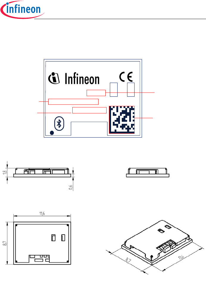
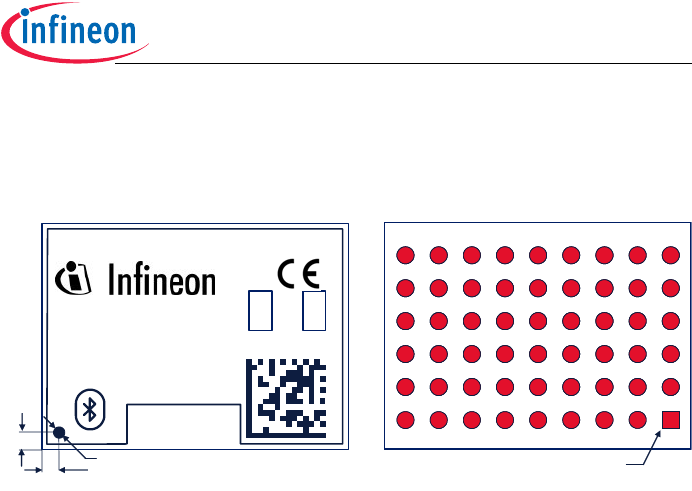
7.1 Package marking
7.2 Production Package
All dimensions are in mm.
Tolerances on all outer dimensions, height, width and length, are +/- 0.2 mm.
PBA 31308 V1.01
FCC ID: Q2331308
G0644 5N605001
Date code
FCC ID
Version
Machine readable
2D date code
UniStone
Package Information
Product Overview 39 T3130-8XV10PO5-7600, 2007-01-31
7.2.1 Pin mark
Pin 1 (A1) is marked on bottom footprint and on the top of the shield on the module
according to Figure 7-1. Diameter of pin 1 mark on the shield is 0.40 mm.
Figure 7-1 Topview and bottom view
PBA 31308 V1.01
FCC ID: Q2331308
G0644 5N605001
0,92
0,92
D=0,4 Pin1 marking bottom side

UniStone
Acronyms & Abbreviations
Product Overview 40 T3130-8XV10PO5-7600, 2007-01-31
8 Acronyms & Abbreviations
Acronym or
abbreviation
Writing out in full
ACK Acknowledgement
ACL Asynchronous Connection-oriented (logical transport)
AFH Adaptive Frequency Hopping
AHS Adaptive Hop Sequence
ARQ Automatic Repeat reQuest
b bit/bits (e.g. kb/s)
B Byte/Bytes (e.g. kB/s)
BALUN BALanced UNbalanced
BD_ADDR Bluetooth Device Address
BER Bit Error Rate
BMU BlueMoon Universal
BOM Bill Of Material
BT Bluetooth
BW Bandwidth
CMOS Complementary Metal Oxide Semiconductor
COD Class Of Device
CODEC COder/DECoder
CPU Central Processing Unit
CQDDR Channel Quality Driven Data Rate
CRC Cyclic Redundancy Check
CTS Clear To Send (UART flow control signal)
CVSD Continuous Variable Slope Delta (modulation)
DC Direct Current
DDC Device Data Control
DM Data Medium-Rate (packet type)
DMA Direct Memory Access
DH Data High-Rate (packet type)
DPSK Differential Phase Shift Keying (modulation)
DQPSK Differential Quaternary Phase Shift Keying (modulation)

UniStone
Acronyms & Abbreviations
Product Overview 41 T3130-8XV10PO5-7600, 2007-01-31
DSP Digital Signal Processor
DUT Device Under Test
CDCT Clock Drift Compensation Task
CQDDR Channel Quality Driven Data Rate
EDR Enhanced Data Rate
EEPROM Electrically Erasable Programmable Read Only Memory
eSCO Extended Synchronous Connection-Oriented (logical transport)
EV Extended Voice (packet type)
FEC Forward Error Correction
FHS Frequency Hop Synchronization (packet)
FIFO First In First Out (buffer)
FM Frequency Modulation
FW Firmware
GFSK Gaussian Frequency Shift Keying (modulation)
GPIO General Purpose Input/Output
GSM Global System for Mobile communication
HCI Host Controller Interface
HCI+ Infineon Specific HCI command set
HEC Header Error Check
HV High quality Voice (packet type)
HW Hardware
I2C Inter-IC Control (bus)
I2S Inter-IC Sound (bus)
IAC Inquiry Access Code
ID IDentifier
IEEE Institute of Electrical and Electronics Engineers
IF Intermediate Frequency
ISM Industrial Scientific & Medical (frequency band)
JTAG Joint Test Action Group
LAN Local Area Network
LAP Lower Address Part
Acronym or
abbreviation
Writing out in full

UniStone
Acronyms & Abbreviations
Product Overview 42 T3130-8XV10PO5-7600, 2007-01-31
LM Link Manager
LMP Link Manager Protocol
LNA Low Noise Amplifier
LO Local Oscillator
LPM Low Power Mode(s)
LSB Least Significant Bit/Byte
LT_ADDR Logical Transport Address
MSB Most Significant Bit/Byte
MSRS Master-Slave Role Switch
NC No Connection
NOP No OPeration
NVM Non-Volatile Memory
OCF Opcode Command Field
OGF Opcode Group Field
PA Power Amplifier
PCB Printed Circuit Board
PCM Pulse Coded Modulation
PDU Protocol Data Unit
PER Packet Error Rate
PIN Personal Identification Number
PLC Packet Loss Concealment
PLL Phase Locked Loop
PMU Power Management Unit
POR Power-On Reset
PTA Packet Traffic Arbitration
PTT Packet Type Table
QoS Quality Of Service
RAM Random Access Memory
RF Radio Frequency
ROM Read Only Memory
RSSI Received Signal Strength Indication
Acronym or
abbreviation
Writing out in full
UniStone
Acronyms & Abbreviations
Product Overview 43 T3130-8XV10PO5-7600, 2007-01-31
RTS Request To Send (UART flow control signal)
RX Receive
RXD Receive Data (UART signal)
SCO Synchronous Connection-Oriented (logical transport)
SIG Special Interest Group (Bluetooth SIG)
SW Software
SYRI Synthesizer Reference Input
TBD To Be Determined
TCK Test Clock (JTAG signal)
TDI Test Data In (JTAG signal)
TDO Test Data Out (JTAG signal)
TL Transport Layer
TMS Test Mode Select (JTAG signal)
TX Transmit
TXD Transmit Data (UART signal)
UART Universal Asynchronous Receiver & Transmitter
ULPM Ultra Low Power Mode
VCO Voltage Controlled Oscillator
WLAN Wireless LAN (Local Area Network)
Acronym or
abbreviation
Writing out in full

http://www.infineon.com
Published by Infineon Technologies AG