Trimble ELIZABETH35 Hi Power Low Band Transmitter User Manual 568454
Trimble Navigation Ltd Hi Power Low Band Transmitter 568454
Trimble >
Contents
- 1. User Manual Low band RF Power Amp
- 2. User Manual Lowband Transmitter
User Manual Low band RF Power Amp
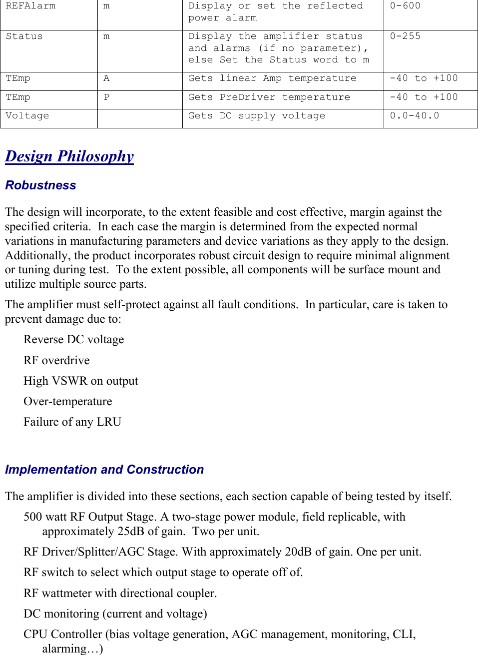
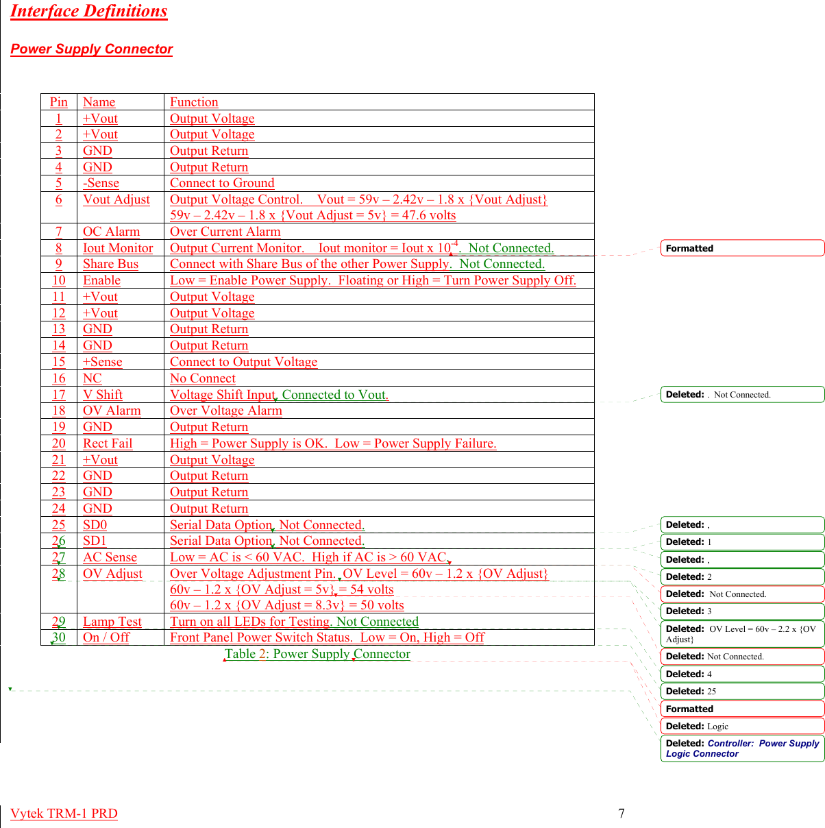
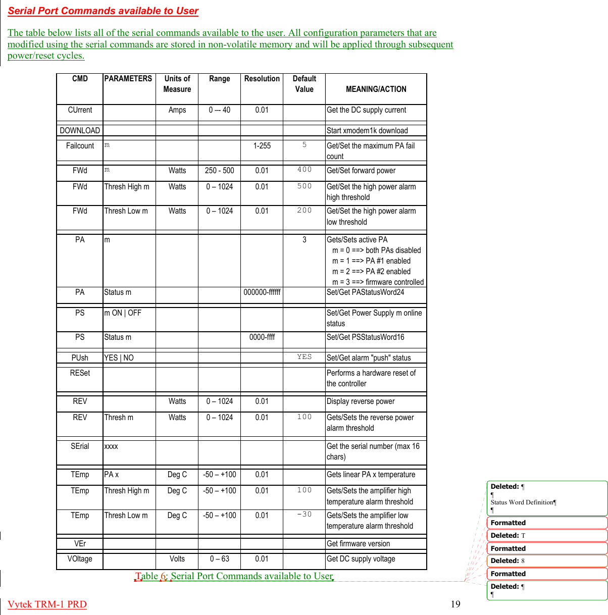
![Vytek TRM-1 PRD 2 TABLE OF CONTENTS Technical Brief.....................................................................................................................3 Scope................................................................................................................................3 Functionality ....................................................................................................................3 Design Philosophy ...............................................................................................................3 Robustness .......................................................................................................................3 Implementation and Construction....................................................................................3 Operation..........................................................................................................................4 Specifications.......................................................................................................................4 Hardware Block Diagram ....................................................................................................6 Interface Definitions ............................................................................................................7 Power Supply Connector .................................................................................................7 Power Amplifier Module Connector ...............................................................................8 Filter / Coupler Module Connector..................................................................................8 Rear Panel DC Power Connector.....................................................................................9 Rear Panel RS232 Connector...........................................................................................9 Controller Connections ..................................................................................................10 FPGA Register Definitions............................................................................................12 Software Description .........................................................................................................13 Alarms Types & Behavior .............................................................................................13 Power Amplifier Alarms............................................................................................13 Power Supply Alarms ................................................................................................15 “Push” Enabling for alarm conditions ...........................................................................15 Alarm Algorithms ..........................................................................................................16 State Machine.................................................................................................................17 PA Cutover.....................................................................................................................18 Manual PA/PS Offline ...................................................................................................18 Serial Port Commands available to User .......................................................................19 LEDs ..................................................................................................................................20 LIST OF TABLES Table 1: Specifications............................................................................................................................................ 5 Table 2: Power Supply Connector .......................................................................................................................... 7 Table 5: Power Amplifier Connector...................................................................................................................... 8 Table 6: Rear Panel RS232 Connector ................................................................................................................... 9 Table 7: Power Amplifier Alarms......................................................................................................................... 13 Table 8: Serial Port Commands available to User................................................................................................ 19 FormattedFormattedFormattedFormattedFormattedFormattedFormattedFormattedFormattedFormattedDeleted: Technical Brief 3¶Scope 3¶Functionality 3¶Design Philosophy 3¶Robustness 3¶Implementation and Construction 3¶Operation 4¶Specifications 4¶Hardware Block Diagram 6¶Interface Definitions 7¶Power Supply Connector 7¶Power Amplifier Module Connector 8¶Filter / Coupler Module Connector 8¶Rear Panel DC Power Connector 9¶Rear Panel RS232 Connector 9¶Controller Connections 10¶FPGA Register Definitions 12¶Software Description 13¶Alarms Types & Behavior 13¶Power Amplifier Alarms 13¶Power Supply Alarms 15¶“Push” Enabling for alarm conditions 15¶Alarm Algorithms 16¶State Machine 17¶PA Cutover 18¶Manual PA/PS Offline 18¶Deleted: Technical Brief 3¶Scope 3¶Deleted: Technical Brief 3¶Scope 3¶Deleted: Technical Brief ¶Scope ¶Deleted: Technical Brief 3¶Scope 3¶Deleted: Technical Brief ¶Scope ¶Deleted: Technical Brief 3¶Scope 3¶Deleted: ¶Deleted: 10Deleted: 14Deleted: 20Deleted: Table 1: Specifications 5¶Table 2: Power Supply Connector 7¶Deleted: Table 1: Specifications 5¶Table 2: Power Supply Connector 7¶Deleted: Table 1: Specifications ¶Table 2: Power Supply Connector ¶Deleted: Table 1: Specifications ¶Table 2: Power Supply Logic ... [2]... [5]... [6]... [12]... [11]... [13]... [4]... [14]... [8]... [15]... [9]... [16]... [7]... [17]... [1]... [18]... [10]... [19]... [3]](https://usermanual.wiki/Trimble/ELIZABETH35.User-Manual-Low-band-RF-Power-Amp/User-Guide-568454-Page-2.png)
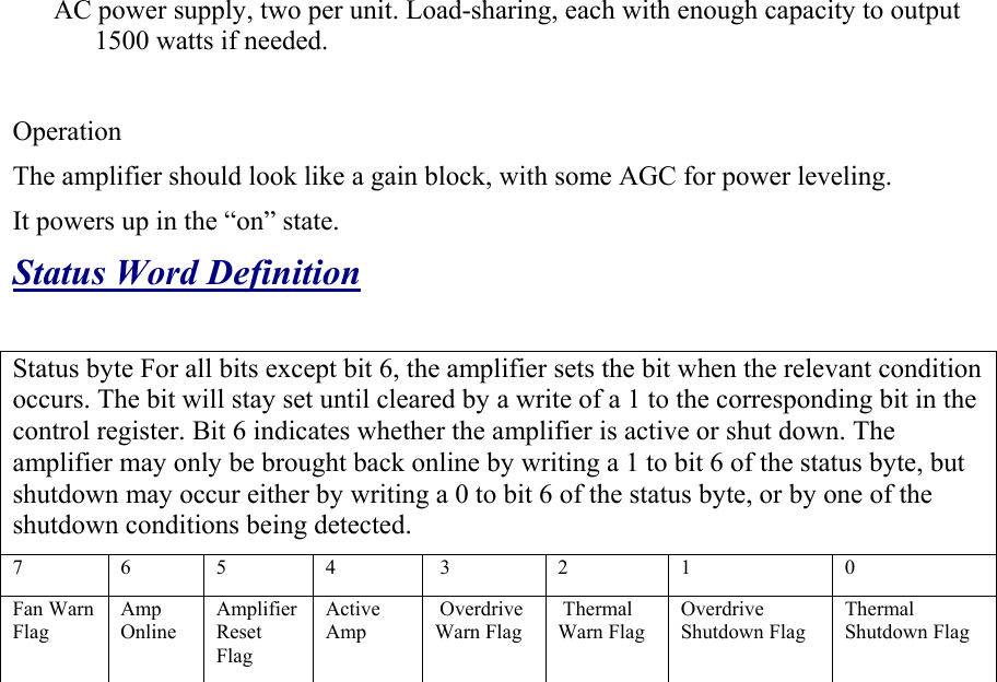
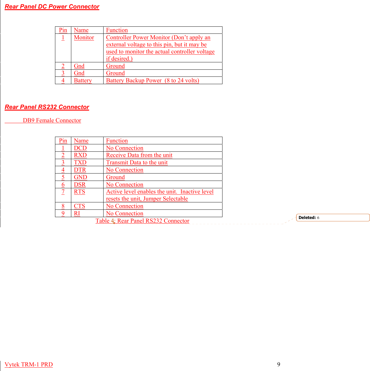
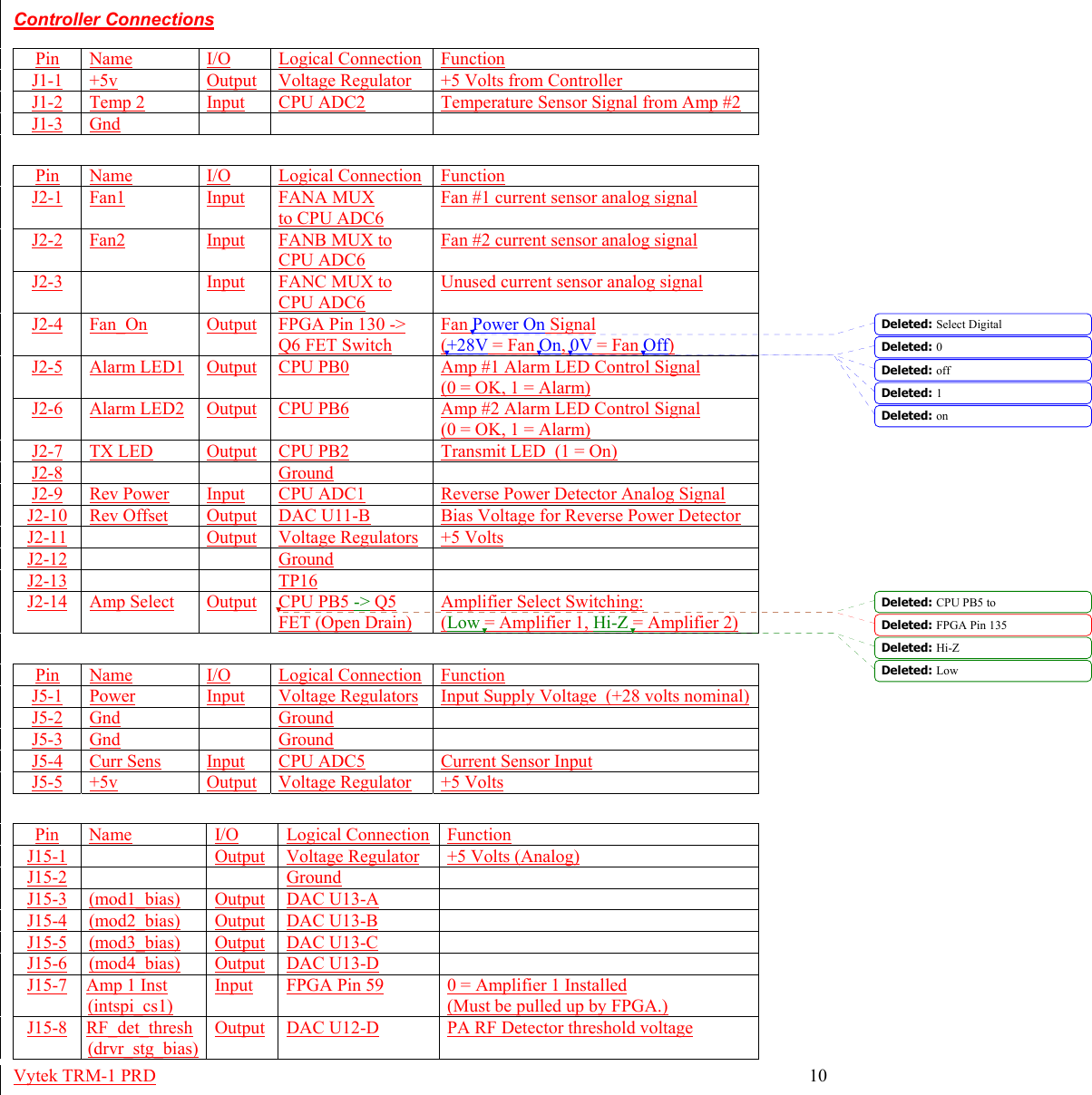
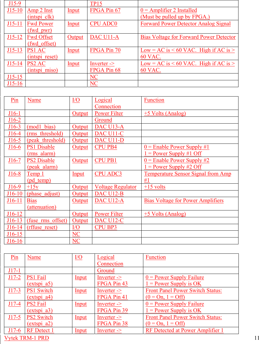
![Vytek TRM-1 PRD 8 Power Amplifier Module Connector Pin Name I/O Function A1 GND Input High Current Ground A2 +48V Input High Current Power Supply (+48 volts) 1 Installed Output “Amplifier Installed” signal to the Controller. Connected to Ground inside of the PA. Floats high when module is not plugged-in. 2 Not Connected 3 V_out Output Low Current Power Supply Loopback to Controller 4 Amp_Select Input Amplifier Select Switching: (+15 volts = Amplifier 1, Low = Amplifier 2) Note: Internal pullup to +15 volts required. 5 +5V_Controller Input +5 volts from the Controller 6 RF_Detect Output RF Input Detector 7 Fan_On Input Fan Power On Signal (+28V = Fan On, 0V = Fan Off) 8 TX_LED Input Drive to the TX LED from Controller 9 RF_det_thresh Input RF Detector threshold voltage from Controller 10 Fan_2 Output Fan #2 Current Sensor Analog Signal 11 Address Input Amplifier Identification: (0 = Amplifier 1, Float = Amplifier 2) 12 Amp_Bias Input Bias Voltage (Analog Control Signal from Controller) 13 Temp Output Temperature analog signal 14 Fan_1 Output Fan #1 current sensor analog signal 15 Alarm LED Input Alarm LED Digital Control Signal (0 = OK, 1 = Alarm) Table 3: Power Amplifier Connector Filter / Coupler Module Connector Pin Name I/O Function 1 Ground 2 +5v_Controller Input +5 volts from Controller 3 Fwd Offset Input Bias Voltage for Forward Power Detector 4 Fwd Power Output Forward Power Detector Analog Signal 5 Rev Offset Input Bias Voltage for Reverse Power Detector 6 Rev Power Output Reverse Power Detector Analog Signal 7 NC 8 NC 9 NC FormattedFormattedFormattedDeleted: Table : Controller: Rear Panel I/O ConnectorDeleted: In1 PwrDeleted: Fwd BiasDeleted: PA #1 Input Power Sensor Analog SignalDeleted: Forward Power BiasDeleted: In2 PwrDeleted: Rev BiasDeleted: PA #2 Input Power Sensor Analog SignalDeleted: Reverse Power BiasDeleted: DriverDeleted: +15VDeleted: BiasDriver Bias SignalTemp1PA #1 Temperature Sensor Analog SignalTemp2PA #2 Temperature Sensor Analog SignalDeleted: Table : Controller: Control & Status Connector¶Deleted: <#>¶Deleted: In PwrDeleted: Input Power Sensor Analog SignalDeleted: Driver BiasDeleted: TempDeleted: DC Voltage… Out to PADeleted: Temperature Sensor Analog SignalDeleted: …Deleted: Low = Amplifier 1, Deleted: BiasA…Deleted: d…Deleted: SDeleted: sDeleted: elect DDeleted: dDeleted: igitalDeleted: …sDeleted: 0…#1…1…#2Deleted: a…sDeleted: GndDeleted: BDeleted: analog Deleted: d…sDeleted: 5Deleted: : Controller... [21]... [26]... [22]... [27]... [29]... [28]... [20]... [30]... [24]... [23]... [25]](https://usermanual.wiki/Trimble/ELIZABETH35.User-Manual-Low-band-RF-Power-Amp/User-Guide-568454-Page-8.png)
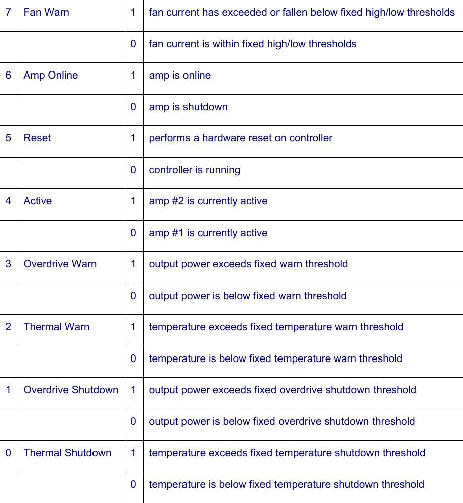
![Vytek TRM-1 PRD 20 LEDs PA #1 and PA #2 will each have LEDs indicating their status, as well as a single Tx LED indicating the presence of RF output greater than 10 Watts. GREEN ● RED ● OFF ● Alarm LED OK Alarm Condition active PA off w/no alarms Tx RF Output No RF Output Formatted: Bullets and NumberingFormattedDeleted: Alarm Behaviour¶All Warn and Shutdown flags remain Deleted: Serial Port Commands available to User¶CMDDeleted: ¶Deleted: Table 1¶¶Alarm Behaviour¶All Warn and Shutdown flags remain ¶... [31]](https://usermanual.wiki/Trimble/ELIZABETH35.User-Manual-Low-band-RF-Power-Amp/User-Guide-568454-Page-20.png)
![Page 2: [1] Deleted Lori Welte 7/2/2003 11:20:00 AM Technical Brief.....................................................................................................................3 Scope................................................................................................................................3 Functionality ....................................................................................................................3 Design Philosophy ...............................................................................................................3 Robustness .......................................................................................................................3 Implementation and Construction....................................................................................3 Operation..........................................................................................................................4 Specifications.......................................................................................................................4 Hardware Block Diagram ....................................................................................................6 Interface Definitions ............................................................................................................7 Power Supply Connector .................................................................................................7 Power Amplifier Module Connector ...............................................................................8 Filter / Coupler Module Connector..................................................................................8 Rear Panel DC Power Connector.....................................................................................9 Rear Panel RS232 Connector...........................................................................................9 Controller Connections ..................................................................................................10 FPGA Register Definitions ............................................................................................12 Software Description .........................................................................................................13 Alarms Types & Behavior .............................................................................................13 Power Amplifier Alarms............................................................................................13 Power Supply Alarms ................................................................................................15 “Push” Enabling for alarm conditions ...........................................................................15 Alarm Algorithms ..........................................................................................................16 State Machine.................................................................................................................17 PA Cutover.....................................................................................................................18 Manual PA/PS Offline ...................................................................................................18 Serial Port Commands available to User .......................................................................19 LEDs ..................................................................................................................................20 Page 2: [2] Deleted Art Lashbrook 7/1/2003 12:46:00 PM Technical Brief.....................................................................................................................3 Scope................................................................................................................................3 Functionality ....................................................................................................................3 Design Philosophy ...............................................................................................................3 Robustness .......................................................................................................................3 Implementation and Construction....................................................................................3 Operation..........................................................................................................................4 Specifications.......................................................................................................................4 Hardware Block Diagram ....................................................................................................6 Interface Definitions ............................................................................................................7 Power Supply Connector .................................................................................................7 Power Amplifier Module Connector ...............................................................................8 Filter / Coupler Module Connector..................................................................................8 Rear Panel DC Power Connector.....................................................................................9 Rear Panel RS232 Connector...........................................................................................9 Controller Connections ..................................................................................................10](https://usermanual.wiki/Trimble/ELIZABETH35.User-Manual-Low-band-RF-Power-Amp/User-Guide-568454-Page-21.png)
![FPGA Register Definitions ............................................................................................12 Software Description .........................................................................................................13 Alarms Types & Behavior .............................................................................................13 Power Amplifier Alarms............................................................................................13 Power Supply Alarms ................................................................................................15 “Push” Enabling for alarm conditions ...........................................................................15 Alarm Algorithms ..........................................................................................................16 State Machine.................................................................................................................17 PA Cutover.....................................................................................................................18 Manual PA/PS Offline ...................................................................................................18 Serial Port Commands available to User .......................................................................19 LEDs ..................................................................................................................................20 Page 2: [3] Deleted Lori Welte 6/23/2003 8:55:00 AM Technical Brief.....................................................................................................................3 Scope................................................................................................................................3 Functionality ....................................................................................................................3 Design Philosophy ...............................................................................................................3 Robustness .......................................................................................................................3 Implementation and Construction....................................................................................3 Operation..........................................................................................................................4 Specifications.......................................................................................................................4 Hardware Block Diagram ....................................................................................................6 Interface Definitions ............................................................................................................7 Power Supply Connector .................................................................................................7 Power Amplifier Module Connector ...............................................................................8 Filter / Coupler Module Connector..................................................................................8 Rear Panel DC Power Connector.....................................................................................9 Rear Panel RS232 Connector...........................................................................................9 Controller Connections ..................................................................................................10 FPGA Register Definitions ............................................................................................12 Software Description .........................................................................................................13 Alarms Types & Behavior .............................................................................................13 Power Amplifier Alarms............................................................................................13 Power Supply Alarms ................................................................................................15 “Push” Enabling for alarm conditions ...........................................................................15 Alarm Algorithms ..........................................................................................................16 State Machine.................................................................................................................17 Serial Port Commands available to User .......................................................................18 LEDs ..................................................................................................................................19 Page 2: [4] Deleted Art Lashbrook 4/10/2003 7:16:00 PM Technical Brief....................................................................................................................... Scope.................................................................................................................................. Functionality ...................................................................................................................... Design Philosophy ................................................................................................................. Robustness .........................................................................................................................](https://usermanual.wiki/Trimble/ELIZABETH35.User-Manual-Low-band-RF-Power-Amp/User-Guide-568454-Page-22.png)
![Implementation and Construction...................................................................................... Operation............................................................................................................................ Specifications......................................................................................................................... System...................................................................................................................................... Power Amp................................................................................................................................... Controller..................................................................................................................................... Hardware Block Diagram ...................................................................................................... Hardware Description ..........................................................................................................7 Mechanical Design...............................................................................................................7 Interconnect Definitions......................................................................................................... Power Supply Logic Connector ......................................................................................... Controller: Rear Panel I/O Connector.............................................................................8 Controller: Control & Status Connector .........................................................................8 Power Amplifier: Controller Connector ........................................................................... Software Description ............................................................................................................. Alarms Types & Behavior ................................................................................................. Power Amplifier Alarms................................................................................................ Power Supply Alarms .................................................................................................... “Push” Enabling for alarm conditions ............................................................................... Alarm Algorithms ..........................................................................................................11 State Machine..................................................................................................................... Serial Port Commands available to User ........................................................................... LEDs ...................................................................................................................................... Page 2: [5] Deleted Lori Welte 4/7/2003 1:54:00 PM Technical Brief.....................................................................................................................3 Scope................................................................................................................................3 Functionality ....................................................................................................................3 Design Philosophy ...............................................................................................................3 Robustness .......................................................................................................................3 Implementation and Construction....................................................................................3 Specifications.......................................................................................................................4 Parameter ............................................................................................................................4 Customer Specification ..........................................................................................................4 Design Goals .......................................................................................................................4 Notes..................................................................................................................................4 System....................................................................................................................................4 Power Amp.................................................................................................................................4 Controller...................................................................................................................................5 Hardware Block Diagram ....................................................................................................6 Hardware Description ..........................................................................................................7 Mechanical Design...............................................................................................................7 Interconnect Definitions.......................................................................................................7 Power Supply Logic Connector .......................................................................................7 Controller: Power Supply Logic Connector ...................................................................7 Controller: Rear Panel I/O Connector.............................................................................8 Controller: Control & Status Connector .........................................................................8 Power Amplifier: Controller Connector .........................................................................9](https://usermanual.wiki/Trimble/ELIZABETH35.User-Manual-Low-band-RF-Power-Amp/User-Guide-568454-Page-23.png)
![Software Description ...........................................................................................................9 Alarms Types & Behavior ...............................................................................................9 Power Amplifier Alarms..............................................................................................9 Power Supply Alarms ................................................................................................10 “Push” Enabling for alarm conditions ...........................................................................10 Alarm Algorithms ..........................................................................................................11 Serial Port Commands available to User .......................................................................12 LEDs ..................................................................................................................................13 Page 2: [6] Deleted Art Lashbrook 4/3/2003 3:56:00 PM Technical Brief....................................................................................................................... Scope.................................................................................................................................. Functionality ...................................................................................................................... Design Philosophy ................................................................................................................. Robustness ......................................................................................................................... Implementation and Construction...................................................................................... Specifications......................................................................................................................... Parameter .............................................................................................................................. Customer Specification ............................................................................................................ Design Goals ......................................................................................................................... Notes.................................................................................................................................... System...................................................................................................................................... Power Amp................................................................................................................................... Controller..................................................................................................................................... Hardware Block Diagram ...................................................................................................... Hardware Description ............................................................................................................ Mechanical Design................................................................................................................. Interconnect Definitions......................................................................................................... Power Supply Logic Connector ......................................................................................... Controller: Power Supply Logic Connector ..................................................................... Controller: Rear Panel I/O Connector............................................................................... Controller: Driver Module Connector .............................................................................. Controller: Power Amplifier Module Connector.............................................................. Controller: RF Output Module Connector........................................................................ Driver: Controller Connector............................................................................................ Power Amplifier: Controller Connector ........................................................................... Software Description ............................................................................................................. Alarms Types & Behavior ................................................................................................. Power Amplifier Alarms................................................................................................ Power Supply Alarms .................................................................................................... “Push” Enabling for alarm conditions ............................................................................... Alarm Algorithms .............................................................................................................. Serial Port Commands available to User ........................................................................... LEDs ...................................................................................................................................... Page 2: [7] Deleted Lori Welte 3/27/2003 11:33:00 AM Technical Brief.....................................................................................................................3 Scope................................................................................................................................3 Functionality ....................................................................................................................3](https://usermanual.wiki/Trimble/ELIZABETH35.User-Manual-Low-band-RF-Power-Amp/User-Guide-568454-Page-24.png)
![Design Philosophy ...............................................................................................................3 Robustness .......................................................................................................................3 Implementation and Construction....................................................................................3 Specifications.......................................................................................................................4 Parameter ............................................................................................................................4 Customer Specification ..........................................................................................................4 Design Goals .......................................................................................................................4 Notes..................................................................................................................................4 System....................................................................................................................................4 Power Amp.................................................................................................................................4 Controller...................................................................................................................................5 Hardware Block Diagram ....................................................................................................6 Hardware Description ..........................................................................................................7 Mechanical Design...............................................................................................................7 Interconnect Definitions.......................................................................................................7 Power Supply Logic Connector .......................................................................................7 Controller: Power Supply Logic Connector ...................................................................7 Controller: Rear Panel I/O Connector.............................................................................8 Controller: Driver Module Connector ............................................................................9 Controller: Power Amplifier Module Connector............................................................9 Controller: RF Output Module Connector....................................................................10 Driver: Controller Connector........................................................................................10 Power Amplifier: Controller Connector .......................................................................11 Software Description .........................................................................................................12 Serial Port Commands available to User .......................................................................12 Status Word Definition ..................................................................................................12 Alarm Behaviour............................................................................................................13 Page 2: [8] Formatted Art Lashbrook 4/10/2003 5:39:00 PM Formatted Page 2: [8] Formatted Art Lashbrook 4/10/2003 5:39:00 PM Formatted Page 2: [9] Formatted Art Lashbrook 4/10/2003 5:40:00 PM Formatted Page 2: [9] Formatted Art Lashbrook 4/10/2003 5:40:00 PM Formatted Page 2: [10] Formatted Art Lashbrook 4/10/2003 5:40:00 PM Formatted Page 2: [10] Formatted Art Lashbrook 4/10/2003 5:40:00 PM Formatted](https://usermanual.wiki/Trimble/ELIZABETH35.User-Manual-Low-band-RF-Power-Amp/User-Guide-568454-Page-25.png)
![Page 2: [11] Formatted Art Lashbrook 4/10/2003 7:19:00 PM Formatted Page 2: [11] Formatted Art Lashbrook 4/10/2003 7:19:00 PM Formatted Page 2: [12] Deleted Lori Welte 7/2/2003 11:21:00 AM Table 1: Specifications.........................................................................................................................................Table 2: Power Supply Connector .......................................................................................................................Table 5: Power Amplifier Connector...................................................................................................................Table 6: Rear Panel RS232 Connector ................................................................................................................Table 7: Power Amplifier Alarms........................................................................................................................Table 8: Serial Port Commands available to User ............................................................................................... Page 2: [13] Formatted Art Lashbrook 4/10/2003 5:39:00 PM Formatted Page 2: [13] Formatted Art Lashbrook 4/10/2003 5:39:00 PM Formatted Page 2: [13] Formatted Art Lashbrook 4/10/2003 5:39:00 PM Formatted Page 2: [13] Formatted Art Lashbrook 4/10/2003 5:40:00 PM Formatted Page 2: [13] Formatted Art Lashbrook 4/10/2003 5:40:00 PM Formatted Page 2: [13] Formatted Art Lashbrook 4/10/2003 5:40:00 PM Formatted Page 2: [13] Formatted Art Lashbrook 4/10/2003 5:40:00 PM Formatted Page 2: [13] Formatted Art Lashbrook 4/10/2003 7:19:00 PM Formatted Page 2: [13] Formatted Art Lashbrook 4/10/2003 7:19:00 PM Formatted Page 2: [14] Deleted Art Lashbrook 7/1/2003 1:12:00 PM Table 1: Specifications.........................................................................................................................................](https://usermanual.wiki/Trimble/ELIZABETH35.User-Manual-Low-band-RF-Power-Amp/User-Guide-568454-Page-26.png)
![Table 2: Power Supply Connector .......................................................................................................................Table 5: Power Amplifier Connector...................................................................................................................Table 6: Rear Panel RS232 Connector ................................................................................................................Table 7: Power Amplifier Alarms........................................................................................................................Table 8: Serial Port Commands available to User ............................................................................................... Page 2: [15] Formatted Art Lashbrook 4/10/2003 5:39:00 PM Formatted Page 2: [15] Formatted Art Lashbrook 4/10/2003 5:39:00 PM Formatted Page 2: [15] Formatted Art Lashbrook 4/10/2003 5:39:00 PM Formatted Page 2: [15] Formatted Art Lashbrook 4/10/2003 5:40:00 PM Formatted Page 2: [15] Formatted Art Lashbrook 4/10/2003 5:40:00 PM Formatted Page 2: [15] Formatted Art Lashbrook 4/10/2003 5:40:00 PM Formatted Page 2: [15] Formatted Art Lashbrook 4/10/2003 5:40:00 PM Formatted Page 2: [15] Formatted Art Lashbrook 4/10/2003 7:19:00 PM Formatted Page 2: [15] Formatted Art Lashbrook 4/10/2003 7:19:00 PM Formatted Page 2: [16] Deleted Lori Welte 6/26/2003 9:14:00 AM Table 1: Specifications.........................................................................................................................................Table 2: Power Supply Connector .......................................................................................................................Table 5: Power Amplifier Connector...................................................................................................................Table 6: Rear Panel RS232 Connector ................................................................................................................Table 7: Power Amplifier Alarms........................................................................................................................Table 8: Serial Port Commands available to User ............................................................................................... Page 2: [17] Formatted Art Lashbrook 4/10/2003 5:39:00 PM](https://usermanual.wiki/Trimble/ELIZABETH35.User-Manual-Low-band-RF-Power-Amp/User-Guide-568454-Page-27.png)
![Formatted Page 2: [17] Formatted Art Lashbrook 4/10/2003 5:39:00 PM Formatted Page 2: [17] Formatted Art Lashbrook 4/10/2003 5:39:00 PM Formatted Page 2: [17] Formatted Art Lashbrook 4/10/2003 5:40:00 PM Formatted Page 2: [17] Formatted Art Lashbrook 4/10/2003 5:40:00 PM Formatted Page 2: [17] Formatted Art Lashbrook 4/10/2003 5:40:00 PM Formatted Page 2: [17] Formatted Art Lashbrook 4/10/2003 5:40:00 PM Formatted Page 2: [17] Formatted Art Lashbrook 4/10/2003 7:19:00 PM Formatted Page 2: [17] Formatted Art Lashbrook 4/10/2003 7:19:00 PM Formatted Page 2: [18] Deleted Art Lashbrook 4/10/2003 7:17:00 PM Table 1: Specifications......................................................................................................................................Table 2: Power Supply Logic Connector..........................................................................................................Table 3: Controller: Rear Panel I/O Connector ...............................................................................................Table 4: Controller: Control & Status Connector............................................................................................Table 5: Power Amplifier: Controller Connector ............................................................................................Table 6: Power Amplifier Alarms ....................................................................................................................Table 7: Serial Port Commands available to User ............................................................................................... Page 2: [19] Formatted Art Lashbrook 4/10/2003 7:17:00 PM Formatted Page 2: [19] Formatted Art Lashbrook 4/10/2003 7:17:00 PM Formatted Page 2: [19] Formatted Art Lashbrook 4/10/2003 7:17:00 PM](https://usermanual.wiki/Trimble/ELIZABETH35.User-Manual-Low-band-RF-Power-Amp/User-Guide-568454-Page-28.png)
![Formatted Page 2: [19] Formatted Art Lashbrook 4/10/2003 7:17:00 PM Formatted Page 2: [19] Formatted Art Lashbrook 4/10/2003 7:17:00 PM Formatted Page 2: [19] Formatted Art Lashbrook 4/10/2003 7:17:00 PM Formatted Page 8: [20] Deleted Lori Welte 4/10/2003 11:18:00 AM Driver Bias Page 8: [20] Deleted Lori Welte 4/10/2003 11:18:00 AM Driver Bias Signal Page 8: [21] Deleted Art Lashbrook 4/10/2003 5:46:00 PM DC Voltage Page 8: [21] Deleted Art Lashbrook 4/10/2003 5:53:00 PM Out to PA Page 8: [22] Deleted Art Lashbrook 5/29/2003 12:26:00 PM Page 8: [22] Deleted Art Lashbrook 4/10/2003 5:53:00 PM g Page 8: [22] Deleted Art Lashbrook 4/10/2003 5:57:00 PM Page 8: [23] Deleted Art Lashbrook 4/10/2003 5:57:00 PM Low = Amplifier 1, Page 8: [23] Deleted Art Lashbrook 4/10/2003 5:57:00 PM High Page 8: [23] Deleted Art Lashbrook 5/29/2003 2:50:00 PM 2 Page 8: [24] Deleted Art Lashbrook 5/29/2003 12:15:00 PM BiasA Page 8: [24] Deleted Art Lashbrook 5/29/2003 12:27:00 PM Bias Transistor A signal Page 8: [25] Deleted Art Lashbrook 5/29/2003 12:38:00 PM d Page 8: [25] Deleted Art Lashbrook 4/10/2003 5:51:00 PM I Page 8: [25] Deleted Art Lashbrook 4/10/2003 5:50:00 PM digital signal Page 8: [26] Deleted Art Lashbrook 4/10/2003 5:51:00 PM](https://usermanual.wiki/Trimble/ELIZABETH35.User-Manual-Low-band-RF-Power-Amp/User-Guide-568454-Page-29.png)
![Page 8: [26] Deleted Art Lashbrook 4/10/2003 5:51:00 PM s Page 8: [27] Deleted John Greene 5/2/2003 1:43:00 PM 0 Page 8: [27] Deleted John Greene 5/2/2003 1:43:00 PM #1 Page 8: [27] Deleted John Greene 5/2/2003 1:43:00 PM 1 Page 8: [27] Deleted John Greene 5/2/2003 1:43:00 PM #2 Page 8: [28] Deleted Art Lashbrook 4/10/2003 5:51:00 PM a Page 8: [28] Deleted Art Lashbrook 4/10/2003 5:51:00 PM s Page 8: [29] Deleted Art Lashbrook 5/29/2003 12:42:00 PM B Page 8: [29] Deleted Art Lashbrook 4/10/2003 5:54:00 PM Bias Transistor B signal Page 8: [30] Deleted Art Lashbrook 4/10/2003 5:55:00 PM d Page 8: [30] Deleted Art Lashbrook 4/10/2003 5:55:00 PM s Page 20: [31] Deleted Art Lashbrook 3/17/2003 2:48:00 PM Serial Port Commands available to User CMD PARAMETERS MEANING/ACTION Digital Range COntrol m Sets the control byte m 0-255 CUrrent Gets the DC supply current. 0.0-19.9 0.0-19.9 FWDRead Display forward power 0-600 FWDSet m Set the desired forward power for internal AGC target. 0-600 FWDAlarm m Display or set the FWD power alarm 0-600 Help Display all commands with their definition PA m Display which PA is active, or set active PA to m. 1-2 RESet Performs a hardware reset of the CONTROLLER. REFRead Display the reflected power output 0-600](https://usermanual.wiki/Trimble/ELIZABETH35.User-Manual-Low-band-RF-Power-Amp/User-Guide-568454-Page-30.png)