Trimble ELIZABETH35 Hi Power Low Band Transmitter User Manual 568454
Trimble Navigation Ltd Hi Power Low Band Transmitter 568454
Trimble >
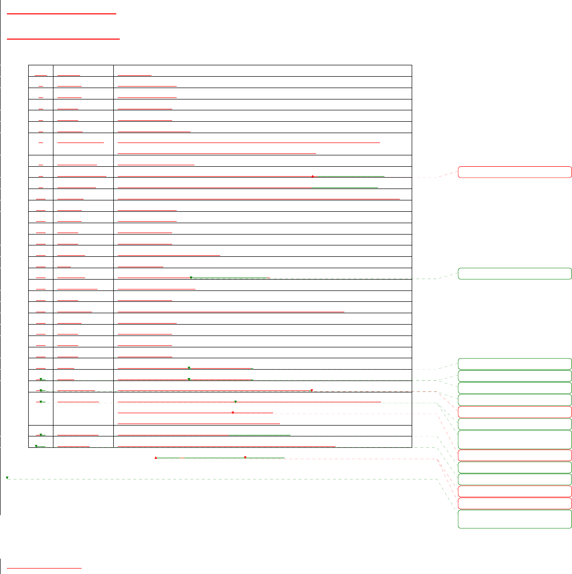
Contents
- 1. User Manual Low band RF Power Amp
- 2. User Manual Lowband Transmitter
User Manual Low band RF Power Amp

Vytek TRM-1 PRD 1
TRM-1
Low-band RF Power Amplifier
Product Requirements Document
Revised August 20, 2003
Vytek Wireless
Wireless Products Division
2310 Cousteau Court
Vista, CA 92083, USA
(760) 536-1000
www.vytek.com
Formatted
Deleted:
Deleted: Version 1A
Deleted: A
p
ril 147, 200331057
Deleted: May 3, 2003
Deleted: Jul
y
1, 2003nel
y
31
Deleted: T
Vytek TRM-1 PRD 2
TABLE OF CONTENTS
Technical Brief.....................................................................................................................3
Scope................................................................................................................................3
Functionality ....................................................................................................................3
Design Philosophy ...............................................................................................................3
Robustness .......................................................................................................................3
Implementation and Construction....................................................................................3
Operation..........................................................................................................................4
Specifications.......................................................................................................................4
Hardware Block Diagram ....................................................................................................6
Interface Definitions ............................................................................................................7
Power Supply Connector .................................................................................................7
Power Amplifier Module Connector ...............................................................................8
Filter / Coupler Module Connector..................................................................................8
Rear Panel DC Power Connector.....................................................................................9
Rear Panel RS232 Connector...........................................................................................9
Controller Connections ..................................................................................................10
FPGA Register Definitions............................................................................................12
Software Description .........................................................................................................13
Alarms Types & Behavior .............................................................................................13
Power Amplifier Alarms............................................................................................13
Power Supply Alarms ................................................................................................15
“Push” Enabling for alarm conditions ...........................................................................15
Alarm Algorithms ..........................................................................................................16
State Machine.................................................................................................................17
PA Cutover.....................................................................................................................18
Manual PA/PS Offline ...................................................................................................18
Serial Port Commands available to User .......................................................................19
LEDs ..................................................................................................................................20
LIST OF TABLES
Table 1: Specifications............................................................................................................................................ 5
Table 2: Power Supply Connector .......................................................................................................................... 7
Table 5: Power Amplifier Connector...................................................................................................................... 8
Table 6: Rear Panel RS232 Connector ................................................................................................................... 9
Table 7: Power Amplifier Alarms......................................................................................................................... 13
Table 8: Serial Port Commands available to User................................................................................................ 19
Formatted
Formatted
Formatted
Formatted
Formatted
Formatted
Formatted
Formatted
Formatted
Formatted
Deleted: Technical Brief 3
Scope 3
Functionality 3
Design Philosophy 3
Robustness 3
Implementation and Construction 3
Operation 4
Specifications 4
Hardware Block Diagram 6
Interface Definitions 7
Power Supply Connector 7
Power Amplifier Module Connector 8
Filter / Coupler Module Connector 8
Rear Panel DC Power Connector 9
Rear Panel RS232 Connector 9
Controller Connections 10
FPGA Register Definitions 12
Software Description 13
Alarms Types & Behavior 13
Power Amplifier Alarms 13
Power Supply Alarms 15
“Push” Enabling for alarm conditions 15
Alarm Algorithms 16
State Machine 17
PA Cutover 18
Manual PA/PS Offline 18
Deleted: Technical Brief 3
Scope 3
Deleted: Technical Brief 3
Scope 3
Deleted: Technical Brief 
Scope 
Deleted: Technical Brief 3
Scope 3
Deleted: Technical Brief 
Scope 
Deleted: Technical Brief 3
Scope 3
Deleted:
Deleted: 10
Deleted: 14
Deleted: 20
Deleted: Table 1: Specifications 5
Table 2: Power Supply Connector 7
Deleted: Table 1: Specifications 5
Table 2: Power Supply Connector 7
Deleted: Table 1: Specifications 
Table 2: Power Supply Connector 
Deleted: Table 1: Specifications 
Table 2: Power Supply Logic
... [2]
... [5]
... [6]
... [12]
... [11]
... [13]
... [4]
... [14]
... [8]
... [15]
... [9]
... [16]
... [7]
... [17]
... [1]
... [18]
... [10]
... [19]
... [3]

Vytek TRM-1 PRD 3
Technical Brief
Scope
The scope of this PRD is to describe the technical implementation of a custom modular Low-Band RF Power
Amplifier Unit. The PA is part of a wide-area data network base station. It is non-linear, with redundancy
built-in for extra reliability and up-time.
Functionality
The amplifier takes in a constant-envelope (CE) RF signal at a level of approximately 5dBm, and amplifies it to
a level of 56dBm (400 watts). The amplifier module and the power supplies are all fully redundant. A CPU
monitors the amplifier, manages alarms, and controls the switching of redundant circuits.
The internal CPU provides a Command Line Interface (CLI) via an RS-232 serial port, for an external device to
monitor and control its operation.
The Amplifier runs off of 90-130V AC input. The CPU controller will also operate off of an external DC input,
if available.
Design Philosophy
Robustness
The design will incorporate, to the extent feasible and cost effective, margin against the specified criteria. In
each case the margin is determined from the expected normal variations in manufacturing parameters and
device variations as they apply to the design. Additionally, the product incorporates robust circuit design to
require minimal alignment or tuning during test. To the extent possible, all components will be surface mount
and utilize multiple source parts.
The amplifier must self-protect against all fault conditions. In particular, care is taken to prevent damage due
to:
1. Reverse DC voltage
2. RF overdrive
3. High VSWR on output
4. Over-temperature
5. Failure of any LRU
Implementation and Construction
The amplifier is divided into these sections, each section capable of being tested by itself.
1. Two field replaceable 500 watt RF Amplifier Modules.
2. An RF switch to select which output stage is routed to the antenna.
3. Lowpass Filter and RF wattmeter with directional coupler.
4. DC monitoring (current and voltage)
5. CPU Controller (bias voltage generation, AGC management, monitoring, CLI, alarming…)
6. Two field replaceable AC power supplies.
Formatted: Bullets and Numbering
Formatted: Bullets and Numbering
Deleted: 
John Sonnenberg
Vytek Wireless
Vista, CA 
Page Break
Deleted: Final PA
Deleted: circuit
Deleted: ,
Deleted: y circuit, the cooling fan, and
the driver circuit
Deleted: Page Break
Vytek TRM-1 PRD 4
Operation
The amplifier should look like a gain block, with some AGC for power leveling.
It powers up in the “on” state.
Specifications
Parameter Customer Specification Design Goals Notes
System
Temperature Range 0 to +50 C ambient -30 to +60 C
Shock So LRUs can be easily packed and
shipped via Fedex
Size 19” open telecom rack mount
TBD height
19” rack mount, 6 U tall, 17” deep.
Weight TBD <50 lbs
Line Replaceable Units PAs/Drivers, Fans, AC-DC Supplies PAs/Drivers, Fans, AC-DC Supplies Plug-in LRUs are hot swappable
MTBF
25,000 hours for soft failures
80,000 hours for hard failures
50,000 soft fail
100,000 hrs hard-fail
Soft failures don’t degrade performance.
Room temperature calculations.
Time To Repair 10 minutes max to replace LRU to fix
soft failure
2 minutes to replace LRUs
EMC, Line Faults and
Lightening Protection
UL Approved AC power supply
Lightening protection on RF output
UL Approved AC power supply
Lightening protection on RF output
15kV ESD on all other I/Os
Hot Standby stages PA, Driver, Fan, AC-DC converter PA, Driver, Fan, AC-DC converters
Power Amp
Power Line Input 110 VAC; 60 Hz
< 10 Amps
90-130VAC, <10A at 110Vac
AC Power Switch and
Breaker
On front or rear panel Rear Panel Bump-proof
Frequency Range 35.15 to 35.75 MHz 32-38 MHz No tuning
Input Signal +5 dBm (+/-3 dB)
50 ohms
single carrier
constant envelope phase modulation
< 40 kHz bandwidth
nominally 2 Hz pulse with 99% duty
<-30dBm in OFF mode,
Rise/Fall time < 5 mS and >100uS
+5 dBm (+/-3 dB)
50 ohms
single carrier
constant envelope phase modulation
< 40 kHz bandwidth
nominally 2 Hz pulse with 99% duty
<-30dBm in OFF mode,
Rise/Fall time < 5 mS and >100uS
Input Connector Panel-mount N-Type female TNC female
Output Power 400 W (+/- 1 dB) Programmable 250-500 watts +/- 1dB
0-50C; +/-1.5dB –30 to +60 C
Harmonics and Spurious Per FCC 22.359 (b)(1)
with 10 dB margin for +/- 50 kHz
Also, close-in spurs (+/- 15 kHz) < -45
dBc
Per FCC 22.359 (b)(1)
with 10 dB margin for +/- 50
kHz
Also, close-in spurs (+/- 15 kHz) < -
45 dBc
Assume “authorized bandwidth” of 20
KHz
Test with pure carrier
Do we need additional limits such as
those for Unintentional Radiators or
Restricted Bands as specified in Part 15?
No
Harmonic Filter All harmonics up to 500MHz, <80dBc Some tower contracts require the use of
a “harmonic filter.” While the
performance of this device isn’t
specified, we should have something in
the P.A. that we can point to and call a
“harmonic filter.”
Type Approvals None None Trimble will take responsibility for this
Output Impedance 50 ohms 50 ohms
Output Match Operate into 2:1 VSWR
No damage into infinite VSWR
Operate into a 3:1. No damage into
infinite VSWR.
Output Connector 7/16 DIN female 7/16 DIN female
Duty Cycle 100 % 100% at up to 500 watts. Will not usually be operated below 50 %
Soft-fail cut-over < 2 Seconds Time to switch over to redundant back-
up circuitry.
Controller
Battery Power Input 10-16 VDC 10-32V Controller operates independent of AC
Formatted
Deleted: Expected Operating
Performance
Deleted: 5
Deleted: 6
Deleted: Multiple chassis may be
appropriate
Deleted:
Deleted: o
Deleted: N
Deleted: <500mS
Deleted: 00
Deleted: mS
Vytek TRM-1 PRD 5
< TBD Amps power to power amp. Battery MUST be
present in order to ensure operation of
controller when amplifier power is off.
Control Interfaces Serial port for local console
Serial port for local console,
38400 bps, N,8,1.
Measurements Voltages, currents, forward and
reflected RF power, temperature, fan
health, alarms, PA stage in use.
Voltages, currents, forward and
reflected RF power, temperature, fan
health, alarms, PA stage in use.
As appropriate on all fans, power
supplies, power amp stages
Alarms Via Control Serial port. Via Control Serial port. LED alarm
status.
Console Protocol VT100 over serial port
XModem or Ymodem for software
upgrading
VT100 over serial port
XModem or XModem/1k for software
upgrading
Network Protocols none none
Connectors DB9 female for console
DB9 Female
Firmware update Via serial port Via serial port
Soft-fail modes Fan monitoring
PA stage
Driver Stage
AC-DC converter
Fan monitoring
PA stage
Driver Stage
AC-DC converter
Failure of any one of these components
will not cause the amplifier to cease
operation.
Hard reset input Via RTS pin on Serial Port Via RTS pin on Serial Port or via
serial command. RTS reset ability
may be defeated by removal of
internal jumper.
Unit is operational when RTS is asserted
and held in reset when not asserted.
Internal Measurement
Accuracy
Power +/- 0.5dB
Voltage +/- 2%
Current +/- 5%
Temperature +/- 3 degrees
Power valid for VSWR < 1.15:1
RF leveling time constant
for changes in drive level.
<10 seconds.
Antenna Switching No “Hot Switching” Power Amplifiers must be in “standby”
or “off” state when changing the antenna
switch setting.
Table 1: Specifications Formatted
Deleted: 192
Deleted: o
Deleted: External alarm output.
Deleted: Ymodem
Deleted: E
Deleted: A PA failure may require a
3dB reduction of power output.
Deleted: i
Deleted: Volatage
Deleted: 
V
Vytek TRM-1 PRD 6
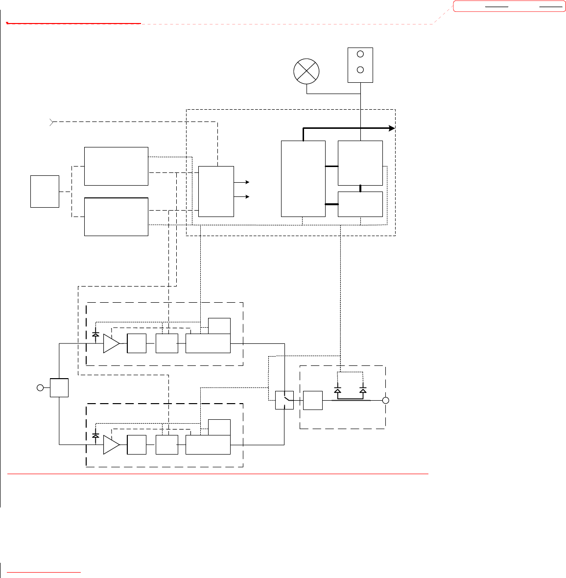
Hardware Block Diagram
Atmel
ATmega128
Processor
FPGA
Atmel
EP1K30
DAC Outputs
Voltage
Regulators
and
Switches
15 volts
5 volts
External
I/O
Connector
A/D Inputs
Controller Module
Power Supply
Module
110
VAC
Input
Tx
Alarm
LEDs
Fans
Power Supply
Module
48 volts
48 volts
Battery
Input
10 to 18 volts
RF Input
TRM-1 Power Amplifier
VyTek Wireless
Control
Control
Power
Amplifier
Driver
Temp
Sensor
Supply Power Analog Controls
and Status
LPF
Input Power
Limiting Amplifier
Power Amplifier Module
Power
Amplifier
Driver
Temp
Sensor
Supply Power Analog Controls
and Status
LPF
Input Power
Limiting Amplifier
Power Amplifier Module
LPF
RF Output Module
RF Output
Fwd Pwr Rev Pwr
Deleted: Page Break
Vytek TRM-1 PRD 7
Interface Definitions
Power Supply Connector
Pin Name Function
1 +Vout Output Voltage
2 +Vout Output Voltage
3 GND Output Return
4 GND Output Return
5 -Sense Connect to Ground
6 Vout Adjust Output Voltage Control. Vout = 59v – 2.42v – 1.8 x {Vout Adjust}
59v – 2.42v – 1.8 x {Vout Adjust = 5v} = 47.6 volts
7 OC Alarm Over Current Alarm
8 Iout Monitor Output Current Monitor. Iout monitor = Iout x 10-4. Not Connected.
9 Share Bus Connect with Share Bus of the other Power Supply. Not Connected.
10 Enable Low = Enable Power Supply. Floating or High = Turn Power Supply Off.
11 +Vout Output Voltage
12 +Vout Output Voltage
13 GND Output Return
14 GND Output Return
15 +Sense Connect to Output Voltage
16 NC No Connect
17 V Shift Voltage Shift Input. Connected to Vout.
18 OV Alarm Over Voltage Alarm
19 GND Output Return
20 Rect Fail High = Power Supply is OK. Low = Power Supply Failure.
21 +Vout Output Voltage
22 GND Output Return
23 GND Output Return
24 GND Output Return
25 SD0 Serial Data Option. Not Connected.
26 SD1 Serial Data Option. Not Connected.
27 AC Sense Low = AC is < 60 VAC. High if AC is > 60 VAC.
28 OV Adjust Over Voltage Adjustment Pin. OV Level = 60v – 1.2 x {OV Adjust}
60v – 1.2 x {OV Adjust = 5v} = 54 volts
60v – 1.2 x {OV Adjust = 8.3v} = 50 volts
29 Lamp Test Turn on all LEDs for Testing. Not Connected
30 On / Off Front Panel Power Switch Status. Low = On, High = Off
Table 2: Power Supply Connector
Formatted
Formatted
Deleted: . Not Connected.
Deleted: ,
Deleted: 1
Deleted: ,
Deleted: 2
Deleted: Not Connected.
Deleted: 3
Deleted: OV Level = 60v – 2.2 x {OV
Adjust}
Deleted: Not Connected.
Deleted: 4
Deleted: 25
Deleted: Logic
Deleted: Controller: Power Supply
Logic Connector
Vytek TRM-1 PRD 8
Power Amplifier Module Connector
Pin Name I/O Function
A1 GND Input High Current Ground
A2 +48V Input High Current Power Supply (+48 volts)
1 Installed Output “Amplifier Installed” signal to the Controller.
Connected to Ground inside of the PA. Floats high when
module is not plugged-in.
2 Not Connected
3 V_out Output Low Current Power Supply Loopback to Controller
4 Amp_Select Input Amplifier Select Switching:
(+15 volts = Amplifier 1, Low = Amplifier 2)
Note: Internal pullup to +15 volts required.
5 +5V_Controller Input +5 volts from the Controller
6 RF_Detect Output RF Input Detector
7 Fan_On Input Fan Power On Signal (+28V = Fan On, 0V = Fan Off)
8 TX_LED Input Drive to the TX LED from Controller
9 RF_det_thresh Input RF Detector threshold voltage from Controller
10 Fan_2 Output Fan #2 Current Sensor Analog Signal
11 Address Input Amplifier Identification:
(0 = Amplifier 1, Float = Amplifier 2)
12 Amp_Bias Input Bias Voltage (Analog Control Signal from Controller)
13 Temp Output Temperature analog signal
14 Fan_1 Output Fan #1 current sensor analog signal
15 Alarm LED Input Alarm LED Digital Control Signal (0 = OK, 1 = Alarm)
Table 3: Power Amplifier Connector
Filter / Coupler Module Connector
Pin Name I/O Function
1 Ground
2 +5v_Controller Input +5 volts from Controller
3 Fwd Offset Input Bias Voltage for Forward Power Detector
4 Fwd Power Output Forward Power Detector Analog Signal
5 Rev Offset Input Bias Voltage for Reverse Power Detector
6 Rev Power Output Reverse Power Detector Analog Signal
7 NC
8 NC
9 NC
Formatted
Formatted
Formatted
Deleted: Table : Controller: Rear Panel
I/O Connector
Deleted: In1 Pwr
Deleted: Fwd Bias
Deleted: PA #1 Input Power Sensor
Analog Signal
Deleted: Forward Power Bias
Deleted: In2 Pwr
Deleted: Rev Bias
Deleted: PA #2 Input Power Sensor
Analog Signal
Deleted: Reverse Power Bias
Deleted: Driver
Deleted: +15V
Deleted: BiasDriver Bias
SignalTemp1PA #1 Temperature Sensor
Analog SignalTemp2PA #2 Temperature
Sensor Analog Signal
Deleted: Table : Controller: Control &
Status Connector
Deleted: <#>
Deleted: In Pwr
Deleted: Input Power Sensor Analog
Signal
Deleted: Driver Bias
Deleted: Temp
Deleted: DC Voltage… Out to PA
Deleted: Temperature Sensor Analog
Signal
Deleted: …
Deleted: Low = Amplifier 1,
Deleted: BiasA…
Deleted: d…
Deleted: S
Deleted: s
Deleted: elect D
Deleted: d
Deleted: igital
Deleted: …s
Deleted: 0…#1…1…#2
Deleted: a…s
Deleted: Gnd
Deleted: B
Deleted: analog
Deleted: d…s
Deleted: 5
Deleted: : Controller
... [21]
... [26]
... [22]
... [27]
... [29]
... [28]
... [20]
... [30]
... [24]
... [23]
... [25]
Vytek TRM-1 PRD 9
Rear Panel DC Power Connector
Pin Name Function
1 Monitor Controller Power Monitor (Don’t apply an
external voltage to this pin, but it may be
used to monitor the actual controller voltage
if desired.)
2 Gnd Ground
3 Gnd Ground
4 Battery Battery Backup Power (8 to 24 volts)
Rear Panel RS232 Connector
DB9 Female Connector
Pin Name Function
1 DCD No Connection
2 RXD Receive Data from the unit
3 TXD Transmit Data to the unit
4 DTR No Connection
5 GND Ground
6 DSR No Connection
7 RTS Active level enables the unit. Inactive level
resets the unit, Jumper Selectable
8 CTS No Connection
9 RI No Connection
Table 4: Rear Panel RS232 Connector Deleted: 6
Vytek TRM-1 PRD 10
Controller Connections
Pin Name I/O Logical Connection Function
J1-1 +5v Output Voltage Regulator +5 Volts from Controller
J1-2 Temp 2 Input CPU ADC2 Temperature Sensor Signal from Amp #2
J1-3 Gnd
Pin Name I/O Logical Connection Function
J2-1 Fan1 Input FANA MUX
to CPU ADC6
Fan #1 current sensor analog signal
J2-2 Fan2 Input FANB MUX to
CPU ADC6
Fan #2 current sensor analog signal
J2-3 Input FANC MUX to
CPU ADC6
Unused current sensor analog signal
J2-4 Fan_On Output FPGA Pin 130 ->
Q6 FET Switch
Fan Power On Signal
(+28V = Fan On, 0V = Fan Off)
J2-5 Alarm LED1 Output CPU PB0 Amp #1 Alarm LED Control Signal
(0 = OK, 1 = Alarm)
J2-6 Alarm LED2 Output CPU PB6 Amp #2 Alarm LED Control Signal
(0 = OK, 1 = Alarm)
J2-7 TX LED Output CPU PB2 Transmit LED (1 = On)
J2-8 Ground
J2-9 Rev Power Input CPU ADC1 Reverse Power Detector Analog Signal
J2-10 Rev Offset Output DAC U11-B Bias Voltage for Reverse Power Detector
J2-11 Output Voltage Regulators +5 Volts
J2-12 Ground
J2-13 TP16
J2-14 Amp Select Output CPU PB5 -> Q5
FET (Open Drain)
Amplifier Select Switching:
(Low = Amplifier 1, Hi-Z = Amplifier 2)
Pin Name I/O Logical Connection Function
J5-1 Power Input Voltage Regulators Input Supply Voltage (+28 volts nominal)
J5-2 Gnd Ground
J5-3 Gnd Ground
J5-4 Curr Sens Input CPU ADC5 Current Sensor Input
J5-5 +5v Output Voltage Regulator +5 Volts
Pin Name I/O Logical Connection Function
J15-1 Output Voltage Regulator +5 Volts (Analog)
J15-2 Ground
J15-3 (mod1_bias) Output DAC U13-A
J15-4 (mod2_bias) Output DAC U13-B
J15-5 (mod3_bias) Output DAC U13-C
J15-6 (mod4_bias) Output DAC U13-D
J15-7 Amp 1 Inst
(intspi_cs1)
Input FPGA Pin 59 0 = Amplifier 1 Installed
(Must be pulled up by FPGA.)
J15-8 RF_det_thresh
(drvr_stg_bias)
Output DAC U12-D PA RF Detector threshold voltage
Deleted: Select Digital
Deleted: 0
Deleted: off
Deleted: 1
Deleted: on
Deleted: CPU PB5 to
Deleted: FPGA Pin 135
Deleted: Hi-Z
Deleted: Low
Vytek TRM-1 PRD 11
J15-9 TP15
J15-10 Amp 2 Inst
(intspi_clk)
Input FPGA Pin 67 0 = Amplifier 2 Installed
(Must be pulled up by FPGA.)
J15-11 Fwd Power
(fwd_pwr)
Input CPU ADC0 Forward Power Detector Analog Signal
J15-12 Fwd Offset
(fwd_offset)
Output DAC U11-A Bias Voltage for Forward Power Detector
J15-13 PS1 AC
(intspi_reset)
Input FPGA Pin 70 Low = AC is < 60 VAC. High if AC is >
60 VAC.
J15-14 PS2 AC
(intspi_miso)
Input Inverter ->
FPGA Pin 68
Low = AC is < 60 VAC. High if AC is >
60 VAC.
J15-15 NC
J15-16 NC
Pin Name I/O Logical
Connection
Function
J16-1 Output Power Filter +5 Volts (Analog)
J16-2 Ground
J16-3 (mod1_bias) Output DAC U13-A
J16-4 (rms_threshold) Output DAC U11-C
J16-5 (peak_threshold) Output DAC U11-D
J16-6 PS1 Disable
(rms_alarm)
Output CPU PB4 0 = Enable Power Supply #1
1 = Power Supply #1 Off
J16-7 PS2 Disable
(peak_alarm)
Output CPU PB1 0 = Enable Power Supply #2
1 = Power Supply #2 Off
J16-8 Temp 1
(pd_temp)
Input CPU ADC3 Temperature Sensor Signal from Amp
#1
J16-9 +15v Output Voltage Regulator +15 volts
J16-10 (phase_adjust) Output DAC U12-B
J16-11 Bias
(attenuation)
Output DAC U12-A Bias Voltage for Power Amplifiers
J16-12 Output Power Filter +5 Volts (Analog)
J16-13 (fuse_rms_offset) Output DAC U12-C
J16-14 (rffuse_reset) I/O CPU BP3
J16-15 NC
J16-16 NC
Pin Name I/O Logical
Connection
Function
J17-1 Ground
J17-2 PS1 Fail
(extspi_a5)
Input Inverter ->
FPGA Pin 43
0 = Power Supply Failure
1 = Power Supply is OK
J17-3 PS1 Switch
(extspi_a4)
Input Inverter ->
FPGA Pin 41
Front Panel Power Switch Status:
(0 = On, 1 = Off)
J17-4 PS2 Fail
(extspi_a3)
Input Inverter ->
FPGA Pin 39
0 = Power Supply Failure
1 = Power Supply is OK
J17-5 PS2 Switch
(extspi_a2)
Input Inverter ->
FPGA Pin 38
Front Panel Power Switch Status:
(0 = On, 1 = Off)
J17-6 RF Detect 1 Input Inverter -> RF Detected at Power Amplifier 1
Vytek TRM-1 PRD 12
(extspi_a1) FPGA Pin 37 (0 = No, 1 = Yes)
J17-7 RF Detect 2
(extspi_a0)
Input Inverter ->
FPGA Pin 36
RF Detected at Power Amplifier 2
(0 = No, 1 = Yes)
J17-8 PS1 OV
(extspi_clk)
Input Inverter ->
FPGA Pin 46
Over Voltage Alarm
J17-9 PS1 OC
(extspi_mosi)
Input Inverter ->
FPGA Pin 48
Over Current Alarm
J17-10 (extspi_miso) Output Inverter ->
FPGA Pin 47
J17-11 PS2 OV
(extspi_backplid0)
Input Inverter ->
FPGA Pin 83
Over Voltage Alarm
J17-12 PS2 OC
(extspi_backplid1)
Input Inverter ->
FPGA Pin 86
Over Current Alarm
J17-13 NC
J17-14 NC
J17-15 Ground
J17-16 NC
FPGA Register Definitions
Note that CS signal from CPU must be set high in order for the FPGA to be selected. This signal comes from
the CPU’s PE2 pin.
Address lines shown are used to select between the internal registers as defined below. All other address lines
are “don’t cares.”
A11 A10 A9 A8 Bit(s) R/W Function
0 1 0 0 0 Read NC – Read as 0
0 1 0 0 1 Read PS1 Front Panel Power Switch Status:
(0 = On, 1 = Off)
0 1 0 0 2 Read PS1 AC Detected (0 = No, 1 = Yes)
0 1 0 0 3 Read NC – Read as 0
0 1 0 0 4 Read NC – Read as 0
0 1 0 0 5 Read PS1 Over Voltage Alarm Input
(1 = OK, 0 = Alarm)
0 1 0 0 6 Read PS1 Over Current Alarm Input
(1 = OK, 0 = Alarm)
0 1 0 0 7 Read PS1 Status:
(0 = Failure, 1 = OK)
0 1 0 1 0 Read NC – Read as 0
0 1 0 1 1 Read PS2 Front Panel Power Switch Status:
(0 = On, 1 = Off)
0 1 0 1 2 Read PS2 AC Detected (0 = No, 1 = Yes)
0 1 0 1 3 Read NC – Read as 0
0 1 0 1 4 Read NC – Read as 0
0 1 0 1 5 Read PS2 Over Voltage Alarm Input
(1 = OK, 0 = Alarm)
0 1 0 1 6 Read PS2 Over Current Alarm Input
Deleted: 1
Deleted: 68h
Deleted: 68h
Deleted: 1
Deleted: 68h
Deleted: 1
Deleted: 68h
Deleted: 1
Deleted: 68h
Deleted: 1
Deleted: 68h
Deleted: 1
Deleted: 0
Deleted: 1
Deleted: 68h
Deleted: 1
Deleted: 0
Deleted: 1
Deleted: 68h
Deleted: 1
Deleted: 0
Deleted: 1
Vytek TRM-1 PRD 13
(1 = OK, 0 = Alarm)
0 1 0 1 7 Read PS2 Status:
(0 = Failure, 1 = OK)
0 1 1 0 7-0 R/W Read / Write Scratch Register
0 1 1 1 0 Read Amp 1 Installed (1 = No, 0 = Yes)
0 1 1 1 1 Read RF Detect 1 (0 = No, 1 = Yes)
0 1 1 1 2 Read NC – Read as 0
0 1 1 1 3 Read NC – Read as 0
0 1 1 1 4 Read Amp 2 Installed (1 = No, 0 = Yes)
0 1 1 1 5 Read RF Detect 2 (0 = No, 1 = Yes)
0 1 1 1 6 Read NC – Read as 0
0 1 1 1 7 Read NC – Read as 0
1 0 0 0 0 Write Fan Control (0 = Off, 1 = On)
1 0 0 0 1 Write DAC_Enable
(0 = Disable DACs, 1 = Enable DACs)
1 0 0 0 2 Write Fan Select A Control
1 0 0 0 3 Write Fan Select B Control
1 1 0 0 7-0 Write DAC1
1 1 0 1 7-0 Write DAC2
1 1 1 0 7-0 Write DAC3
1 1 1 1 7-0 Write DAC4
Software Description
Alarms Types & Behavior
Power Amplifier Alarms
The table below lists all of the power amplifier alarm types and the cutover behavior of each alarm.
Table 5: Power Amplifier Alarms
Alarm Type
Status Byte
bit PA #1 Alarm Occurrence PA #2 Alarm Occurrence
Fan Failure 7 Cut to PA #2 Cut to PA #1
High Reverse 6Shutdown Shutdown
Low Pw
r
5 Cut to PA #2 Stay at PA #2
cut back and forth to PA #1
Overcurrent 3 Cut to PA #2 Cut to PA #1 & PA #2,"failcount" times
(to find non-cut condition)
Thermal 2 Cut to PA #2 Cut to PA #1
High Pw
r
1 Cut to PA #2 Cut to PA #1
Formatted
Deleted: 0
Deleted: 1
Deleted: 0
Deleted: 1
Deleted: 0
Deleted: 1
Deleted: #1 Low Byte
Deleted: 7-0
Deleted: Write
Deleted: DAC1 #1 High Byte
Deleted: 7-0
Deleted: Write
Deleted: DAC1 #2 Low Byte
Deleted: 7-0
Deleted: Write
Deleted: DAC1 #2 High Byte
Deleted: 
Deleted: 7

Vytek TRM-1 PRD 14
Status information for both PA #1 and PA #2 is read via a 3 byte (24-bit) status word called PAStatusWord24,
as described below. The amplifier sets the bit when the relevant condition occurs. The bit will stay set until
cleared by a write of a 0 to the corresponding bit in the status register –OR– when the alarming amplifier is
removed or taken offline, then manually brought back online (the failure count will also be cleared in this case).
PAStatusWord24: There is a 3 byte (24-bit) status word:
Byte #1: Generic Info
7, 6 5, 4, 3 2,1,0
Active PA PA #1 failures causing cutover PA #2 failures causing cutover
00 = none 000=0 000=0
01 = PA #1 001=1 001=1
10 = PA #2 010=2 010=2
11 = INVALID 011=3 011=3
100=4 100=4
NOTE: these bits 101=5 101=5
are READ ONLY 110=6 110=6
111=7+ 111=7+
Byte #2: PA#1 Status Byte
765 43210
Fan Warn High Reverse Low Pwr Overcurrent Thermal High Pwr NotInstalled
Byte #3: PA#2 Status Byte
76 543210
Fan Warn High Reverse Low Pwr Overcurrent Thermal High Pwr NotInstalled
** All alarm bits in PA #1 and PA #2 are latched, and remain set even if the condition has gone away with or without transmission
except the NotInstalled flag (bit 0)
Deleted: 
Vytek TRM-1 PRD 15
Power Supply Alarms
In addition to the power amplifier alarms, Status information for both PS #1 and PS #2 is read via a 2 byte (16-
bit) status word called PSStatusWord16, as described below. The amplifier sets the bit when the relevant
condition occurs. The bit will stay set until cleared by a write of a 0 to the corresponding bit in the status
register.
“Push” Enabling for alarm conditions
The TRM-1 can be configured to send unsolicited alarm information (see command table below) on the
occurrence of a power amplifier or power supply alarm. The unsolicited alarm information is sent as
PAStatusWord24 or PSStatusWord16 through the serial port. It is sent once on the setting of any alarm bits in
Byte 2 or Byte 3 of PAStatusWord24, or if a Power Supply alarm occurs, Byte 1 or Byte 2 in PSStatusWord16.
The pushed alarm status word will be sent in ASCII format (as are all commands and responses). It will have
the following format. Note that numeric values are given in hex.
PAStatusWord24=488000
or
PSStatusWord16=0400
By default, alarm “push” is enabled.
PSStatusWord16: There is a 2 byte (8-bit) status word:
Byte #1: PS#1 Status Byte
7 65 4 3210
Fail Overcurrent Overvoltage ACSense SwitchOn Offline
0 = good 0 = on
Byte #2: PS#2 Status Byte 1 = bad 1 = off
7 6 5 4 3210
Fail Overcurrent Overvoltage ACSense SwitchOn Offline
Formatted
Formatted
Deleted: 
Deleted: :
Deleted: disabled
Vytek TRM-1 PRD 16
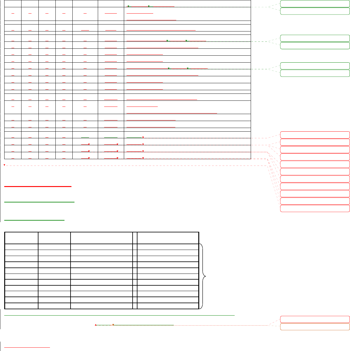
Alarm Algorithms
Several alarm scenarios are described in the flow diagrams below.
Power On:
enable active P
A
Update LEDs on active
PA
Update LEDs on
inactive PA
Send StatusWord24, if
PAn Status Byte != 0
p
ush enabled
PA #1 Alarms with Fan Failure
PA #1 Fan Failure
detected
Inc PA #1 fail count
Update PA #1 LED
PA #2 fail count < TBD
Switch to PA #2
Send StatusWord24
p
ush enabled
PA #1 Alarms with Fan Failure
& PA #2 Alarms with Thermal
PA #2 Thermal
detected
Inc PA #2 fail count
Update PA #2 LED
PA #1 fail count > TBD
Shutdown
Send StatusWord24
p
ush enabled
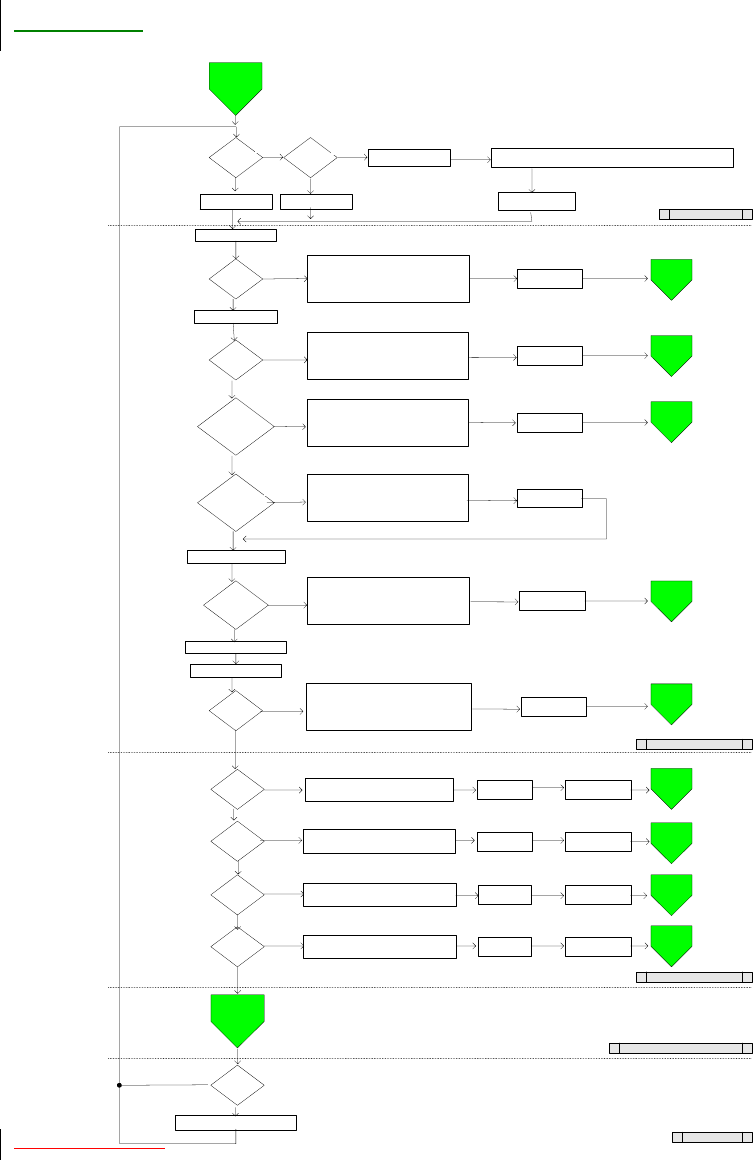
Vytek TRM-1 PRD 17
State Machine
no
yes
no
yes
no
yes
yes
yes
no
no
no
yes
no
yes
no
no
yes
yes
no
no
no
Read temperature
temp >
100?
Read Fan current
Fans OK?
Read Reflected Power
Ref Pwr >
rev_thresh?
Read DC Voltage
Read DC Current
newlline
entered?
Process CLI cmd
PAStatWord24:Set Thermal Alarm Flag
Change active PA #
Inc PA fail counter
Set LED red
TRM-1 CPU Controller: State Machine
PA Alarm Control
CLI
Temperature
Alarm
Fan Fail
Alarm
High Reverse
Alarm
High Pwr
Alarm
Excess
current?
PAStatWord24:Set Fan Fail Flag
Change active PA #
Inc PA fail counter
Set LED red
Low Pwr
Alarm
Overcurrent
Alarm
Power Leveling
RFdetect
== 0?
measured_fwd
>high thresh?
PAStatWord24:Set High Pwr Flag
Change active PA #
Inc PA fail counter
Set LED red
measured_fwd
< low thresh?
yes PAStatWord24:Set Low Pwr Flag Set LED red
PAStatWord24:Set High Reverse Flag
Change active PA #
Inc PA fail counter
yes
no
PAStatWord24:Set Overcurrent Flag
Change active PA #
Inc PA fail counter
PS Alarm Control
PSFail
high?
OCAlarm
high?
yes
OVAlarm
high?
PSStatWord16:Set Fail Flag
Set Offline Flag
Set LED red
Set LED red
PSStatWord16:Set Overcurrent Flag
Set Offline Flag
PSStatWord16:Set Overcurrent Flag
Set Offline Flag
Disable PS
Disable PS
Disable PS
RampUp
true?
yes
no
atten = (0.03125*(FwdTarg - FwdRead)) / 0.25 + atten_prev
atten_prev = attenRampUp = falseRampUp = true
Read forward pwr
Set LED red
Set LED red
Set LED red
ACSense
bad?
PSStatWord16:Set ACSense Flag
Set Offline Flag Disable PS Set LED red
PA & PS Offline Mgmt
Initialization
Amp
Cutover
Amp
Cutover
Amp
Cutover
Amp
Cutover
Amp
Cutover
Amp
Cutover
Amp
Cutover
Amp
Cutover
Amp
Cutover
Manual PA/
PS Offline
Vytek TRM-1 PRD 18
PA Cutover
Manual PA/PS Offline
no
yes
no
yes
no
PAx fail: Cutover to PAy
Deselect PAx,
select PAy
PSx disable
PSy enable
PAy fail
counter >=
MAXFAIL
Return to State
Machine
PSy switch
off?
CLI cmd
override?
yes
no
yes
yes
no
Manual PA/PS offline
mgmt
PS x currently
offline (switch or
SW)?
Clear PA x fail
counter
PA x currently
installed?
Clear PA x
alarms
Return to State
Machine
Vytek TRM-1 PRD 19
Serial Port Commands available to User
The table below lists all of the serial commands available to the user. All configuration parameters that are
modified using the serial commands are stored in non-volatile memory and will be applied through subsequent
power/reset cycles.
Table 6: Serial Port Commands available to User
CUrrent Amps 0 –- 40 0.01 Get the DC supply current
DOWNLOAD Start xmodem1k download
Failcount m1-255 5Get/Set the maximum PA fail
count
FWd mWatts 250 - 500 0.01 400 Get/Set forward power
FWd Thresh High m Watts 0 – 1024 0.01 500 Get/Set the high power alarm
high threshold
FWd Thresh Low m Watts 0 – 1024 0.01 200 Get/Set the high power alarm
low threshold
PA m 3 Gets/Sets active PA
m = 0 ==> both PAs disabled
m = 1 ==> PA #1 enabled
m = 2 ==> PA #2 enabled
m = 3 ==> firmware controlled
PA Status m 000000-ffffff Set/Get PAStatusWord24
PS m ON | OFF Set/Get Power Supply m online
status
PS Status m 0000-ffff Set/Get PSStatusWord16
PUsh YES | NO YES Set/Get alarm "push" status
RESet Performs a hardware reset of
the controller
REV Watts 0 – 1024 0.01 Display reverse power
REV Thresh m Watts 0 – 1024 0.01 100 Gets/Sets the reverse power
alarm threshold
SErial xxxx Get the serial number (max 16
chars)
TEmp PA x Deg C -50 – +100 0.01 Gets linear PA x temperature
TEmp Thresh High m Deg C -50 – +100 0.01 100 Gets/Sets the amplifier high
temperature alarm threshold
TEmp Thresh Low m Deg C -50 – +100 0.01 -30 Gets/Sets the amplifier low
temperature alarm threshold
VEr Get firmware version
VOltage Volts 0 – 63 0.01 Get DC supply voltage
Resolution Default
Value
MEANING/ACTION
CMD PARAMETERS Units of
Measure
Range
Formatted
Formatted
Formatted
Deleted: 
Status Word Definition
Deleted: T
Deleted: 8
Deleted: 
Vytek TRM-1 PRD 20
LEDs
PA #1 and PA #2 will each have LEDs indicating their status, as well as a single Tx LED indicating the
presence of RF output greater than 10 Watts.
GREEN ● RED ● OFF ●
Alarm LED OK Alarm Condition
active
PA off w/no
alarms
Tx RF Output No RF Output
Formatted: Bullets and Numbering
Formatted
Deleted: Alarm Behaviour
All Warn and Shutdown flags remain
Deleted: Serial Port Commands
available to User
CMD
Deleted: 
Deleted: Table 1
Alarm Behaviour
All Warn and Shutdown flags remain 
... [31]

Page 2: [1] Deleted Lori Welte 7/2/2003 11:20:00 AM
Technical Brief.....................................................................................................................3
Scope................................................................................................................................3
Functionality ....................................................................................................................3
Design Philosophy ...............................................................................................................3
Robustness .......................................................................................................................3
Implementation and Construction....................................................................................3
Operation..........................................................................................................................4
Specifications.......................................................................................................................4
Hardware Block Diagram ....................................................................................................6
Interface Definitions ............................................................................................................7
Power Supply Connector .................................................................................................7
Power Amplifier Module Connector ...............................................................................8
Filter / Coupler Module Connector..................................................................................8
Rear Panel DC Power Connector.....................................................................................9
Rear Panel RS232 Connector...........................................................................................9
Controller Connections ..................................................................................................10
FPGA Register Definitions ............................................................................................12
Software Description .........................................................................................................13
Alarms Types & Behavior .............................................................................................13
Power Amplifier Alarms............................................................................................13
Power Supply Alarms ................................................................................................15
“Push” Enabling for alarm conditions ...........................................................................15
Alarm Algorithms ..........................................................................................................16
State Machine.................................................................................................................17
PA Cutover.....................................................................................................................18
Manual PA/PS Offline ...................................................................................................18
Serial Port Commands available to User .......................................................................19
LEDs ..................................................................................................................................20
Page 2: [2] Deleted Art Lashbrook 7/1/2003 12:46:00 PM
Technical Brief.....................................................................................................................3
Scope................................................................................................................................3
Functionality ....................................................................................................................3
Design Philosophy ...............................................................................................................3
Robustness .......................................................................................................................3
Implementation and Construction....................................................................................3
Operation..........................................................................................................................4
Specifications.......................................................................................................................4
Hardware Block Diagram ....................................................................................................6
Interface Definitions ............................................................................................................7
Power Supply Connector .................................................................................................7
Power Amplifier Module Connector ...............................................................................8
Filter / Coupler Module Connector..................................................................................8
Rear Panel DC Power Connector.....................................................................................9
Rear Panel RS232 Connector...........................................................................................9
Controller Connections ..................................................................................................10

FPGA Register Definitions ............................................................................................12
Software Description .........................................................................................................13
Alarms Types & Behavior .............................................................................................13
Power Amplifier Alarms............................................................................................13
Power Supply Alarms ................................................................................................15
“Push” Enabling for alarm conditions ...........................................................................15
Alarm Algorithms ..........................................................................................................16
State Machine.................................................................................................................17
PA Cutover.....................................................................................................................18
Manual PA/PS Offline ...................................................................................................18
Serial Port Commands available to User .......................................................................19
LEDs ..................................................................................................................................20
Page 2: [3] Deleted Lori Welte 6/23/2003 8:55:00 AM
Technical Brief.....................................................................................................................3
Scope................................................................................................................................3
Functionality ....................................................................................................................3
Design Philosophy ...............................................................................................................3
Robustness .......................................................................................................................3
Implementation and Construction....................................................................................3
Operation..........................................................................................................................4
Specifications.......................................................................................................................4
Hardware Block Diagram ....................................................................................................6
Interface Definitions ............................................................................................................7
Power Supply Connector .................................................................................................7
Power Amplifier Module Connector ...............................................................................8
Filter / Coupler Module Connector..................................................................................8
Rear Panel DC Power Connector.....................................................................................9
Rear Panel RS232 Connector...........................................................................................9
Controller Connections ..................................................................................................10
FPGA Register Definitions ............................................................................................12
Software Description .........................................................................................................13
Alarms Types & Behavior .............................................................................................13
Power Amplifier Alarms............................................................................................13
Power Supply Alarms ................................................................................................15
“Push” Enabling for alarm conditions ...........................................................................15
Alarm Algorithms ..........................................................................................................16
State Machine.................................................................................................................17
Serial Port Commands available to User .......................................................................18
LEDs ..................................................................................................................................19
Page 2: [4] Deleted Art Lashbrook 4/10/2003 7:16:00 PM
Technical Brief.......................................................................................................................
Scope..................................................................................................................................
Functionality ......................................................................................................................
Design Philosophy .................................................................................................................
Robustness .........................................................................................................................

Implementation and Construction......................................................................................
Operation............................................................................................................................
Specifications.........................................................................................................................
System......................................................................................................................................
Power Amp...................................................................................................................................
Controller.....................................................................................................................................
Hardware Block Diagram ......................................................................................................
Hardware Description ..........................................................................................................7
Mechanical Design...............................................................................................................7
Interconnect Definitions.........................................................................................................
Power Supply Logic Connector .........................................................................................
Controller: Rear Panel I/O Connector.............................................................................8
Controller: Control & Status Connector .........................................................................8
Power Amplifier: Controller Connector ...........................................................................
Software Description .............................................................................................................
Alarms Types & Behavior .................................................................................................
Power Amplifier Alarms................................................................................................
Power Supply Alarms ....................................................................................................
“Push” Enabling for alarm conditions ...............................................................................
Alarm Algorithms ..........................................................................................................11
State Machine.....................................................................................................................
Serial Port Commands available to User ...........................................................................
LEDs ......................................................................................................................................
Page 2: [5] Deleted Lori Welte 4/7/2003 1:54:00 PM
Technical Brief.....................................................................................................................3
Scope................................................................................................................................3
Functionality ....................................................................................................................3
Design Philosophy ...............................................................................................................3
Robustness .......................................................................................................................3
Implementation and Construction....................................................................................3
Specifications.......................................................................................................................4
Parameter ............................................................................................................................4
Customer Specification ..........................................................................................................4
Design Goals .......................................................................................................................4
Notes..................................................................................................................................4
System....................................................................................................................................4
Power Amp.................................................................................................................................4
Controller...................................................................................................................................5
Hardware Block Diagram ....................................................................................................6
Hardware Description ..........................................................................................................7
Mechanical Design...............................................................................................................7
Interconnect Definitions.......................................................................................................7
Power Supply Logic Connector .......................................................................................7
Controller: Power Supply Logic Connector ...................................................................7
Controller: Rear Panel I/O Connector.............................................................................8
Controller: Control & Status Connector .........................................................................8
Power Amplifier: Controller Connector .........................................................................9

Software Description ...........................................................................................................9
Alarms Types & Behavior ...............................................................................................9
Power Amplifier Alarms..............................................................................................9
Power Supply Alarms ................................................................................................10
“Push” Enabling for alarm conditions ...........................................................................10
Alarm Algorithms ..........................................................................................................11
Serial Port Commands available to User .......................................................................12
LEDs ..................................................................................................................................13
Page 2: [6] Deleted Art Lashbrook 4/3/2003 3:56:00 PM
Technical Brief.......................................................................................................................
Scope..................................................................................................................................
Functionality ......................................................................................................................
Design Philosophy .................................................................................................................
Robustness .........................................................................................................................
Implementation and Construction......................................................................................
Specifications.........................................................................................................................
Parameter ..............................................................................................................................
Customer Specification ............................................................................................................
Design Goals .........................................................................................................................
Notes....................................................................................................................................
System......................................................................................................................................
Power Amp...................................................................................................................................
Controller.....................................................................................................................................
Hardware Block Diagram ......................................................................................................
Hardware Description ............................................................................................................
Mechanical Design.................................................................................................................
Interconnect Definitions.........................................................................................................
Power Supply Logic Connector .........................................................................................
Controller: Power Supply Logic Connector .....................................................................
Controller: Rear Panel I/O Connector...............................................................................
Controller: Driver Module Connector ..............................................................................
Controller: Power Amplifier Module Connector..............................................................
Controller: RF Output Module Connector........................................................................
Driver: Controller Connector............................................................................................
Power Amplifier: Controller Connector ...........................................................................
Software Description .............................................................................................................
Alarms Types & Behavior .................................................................................................
Power Amplifier Alarms................................................................................................
Power Supply Alarms ....................................................................................................
“Push” Enabling for alarm conditions ...............................................................................
Alarm Algorithms ..............................................................................................................
Serial Port Commands available to User ...........................................................................
LEDs ......................................................................................................................................
Page 2: [7] Deleted Lori Welte 3/27/2003 11:33:00 AM
Technical Brief.....................................................................................................................3
Scope................................................................................................................................3
Functionality ....................................................................................................................3

Design Philosophy ...............................................................................................................3
Robustness .......................................................................................................................3
Implementation and Construction....................................................................................3
Specifications.......................................................................................................................4
Parameter ............................................................................................................................4
Customer Specification ..........................................................................................................4
Design Goals .......................................................................................................................4
Notes..................................................................................................................................4
System....................................................................................................................................4
Power Amp.................................................................................................................................4
Controller...................................................................................................................................5
Hardware Block Diagram ....................................................................................................6
Hardware Description ..........................................................................................................7
Mechanical Design...............................................................................................................7
Interconnect Definitions.......................................................................................................7
Power Supply Logic Connector .......................................................................................7
Controller: Power Supply Logic Connector ...................................................................7
Controller: Rear Panel I/O Connector.............................................................................8
Controller: Driver Module Connector ............................................................................9
Controller: Power Amplifier Module Connector............................................................9
Controller: RF Output Module Connector....................................................................10
Driver: Controller Connector........................................................................................10
Power Amplifier: Controller Connector .......................................................................11
Software Description .........................................................................................................12
Serial Port Commands available to User .......................................................................12
Status Word Definition ..................................................................................................12
Alarm Behaviour............................................................................................................13
Page 2: [8] Formatted Art Lashbrook 4/10/2003 5:39:00 PM
Formatted
Page 2: [8] Formatted Art Lashbrook 4/10/2003 5:39:00 PM
Formatted
Page 2: [9] Formatted Art Lashbrook 4/10/2003 5:40:00 PM
Formatted
Page 2: [9] Formatted Art Lashbrook 4/10/2003 5:40:00 PM
Formatted
Page 2: [10] Formatted Art Lashbrook 4/10/2003 5:40:00 PM
Formatted
Page 2: [10] Formatted Art Lashbrook 4/10/2003 5:40:00 PM
Formatted

Page 2: [11] Formatted Art Lashbrook 4/10/2003 7:19:00 PM
Formatted
Page 2: [11] Formatted Art Lashbrook 4/10/2003 7:19:00 PM
Formatted
Page 2: [12] Deleted Lori Welte 7/2/2003 11:21:00 AM
Table 1: Specifications.........................................................................................................................................
Table 2: Power Supply Connector .......................................................................................................................
Table 5: Power Amplifier Connector...................................................................................................................
Table 6: Rear Panel RS232 Connector ................................................................................................................
Table 7: Power Amplifier Alarms........................................................................................................................
Table 8: Serial Port Commands available to User ...............................................................................................
Page 2: [13] Formatted Art Lashbrook 4/10/2003 5:39:00 PM
Formatted
Page 2: [13] Formatted Art Lashbrook 4/10/2003 5:39:00 PM
Formatted
Page 2: [13] Formatted Art Lashbrook 4/10/2003 5:39:00 PM
Formatted
Page 2: [13] Formatted Art Lashbrook 4/10/2003 5:40:00 PM
Formatted
Page 2: [13] Formatted Art Lashbrook 4/10/2003 5:40:00 PM
Formatted
Page 2: [13] Formatted Art Lashbrook 4/10/2003 5:40:00 PM
Formatted
Page 2: [13] Formatted Art Lashbrook 4/10/2003 5:40:00 PM
Formatted
Page 2: [13] Formatted Art Lashbrook 4/10/2003 7:19:00 PM
Formatted
Page 2: [13] Formatted Art Lashbrook 4/10/2003 7:19:00 PM
Formatted
Page 2: [14] Deleted Art Lashbrook 7/1/2003 1:12:00 PM
Table 1: Specifications.........................................................................................................................................

Table 2: Power Supply Connector .......................................................................................................................
Table 5: Power Amplifier Connector...................................................................................................................
Table 6: Rear Panel RS232 Connector ................................................................................................................
Table 7: Power Amplifier Alarms........................................................................................................................
Table 8: Serial Port Commands available to User ...............................................................................................
Page 2: [15] Formatted Art Lashbrook 4/10/2003 5:39:00 PM
Formatted
Page 2: [15] Formatted Art Lashbrook 4/10/2003 5:39:00 PM
Formatted
Page 2: [15] Formatted Art Lashbrook 4/10/2003 5:39:00 PM
Formatted
Page 2: [15] Formatted Art Lashbrook 4/10/2003 5:40:00 PM
Formatted
Page 2: [15] Formatted Art Lashbrook 4/10/2003 5:40:00 PM
Formatted
Page 2: [15] Formatted Art Lashbrook 4/10/2003 5:40:00 PM
Formatted
Page 2: [15] Formatted Art Lashbrook 4/10/2003 5:40:00 PM
Formatted
Page 2: [15] Formatted Art Lashbrook 4/10/2003 7:19:00 PM
Formatted
Page 2: [15] Formatted Art Lashbrook 4/10/2003 7:19:00 PM
Formatted
Page 2: [16] Deleted Lori Welte 6/26/2003 9:14:00 AM
Table 1: Specifications.........................................................................................................................................
Table 2: Power Supply Connector .......................................................................................................................
Table 5: Power Amplifier Connector...................................................................................................................
Table 6: Rear Panel RS232 Connector ................................................................................................................
Table 7: Power Amplifier Alarms........................................................................................................................
Table 8: Serial Port Commands available to User ...............................................................................................
Page 2: [17] Formatted Art Lashbrook 4/10/2003 5:39:00 PM

Formatted
Page 2: [17] Formatted Art Lashbrook 4/10/2003 5:39:00 PM
Formatted
Page 2: [17] Formatted Art Lashbrook 4/10/2003 5:39:00 PM
Formatted
Page 2: [17] Formatted Art Lashbrook 4/10/2003 5:40:00 PM
Formatted
Page 2: [17] Formatted Art Lashbrook 4/10/2003 5:40:00 PM
Formatted
Page 2: [17] Formatted Art Lashbrook 4/10/2003 5:40:00 PM
Formatted
Page 2: [17] Formatted Art Lashbrook 4/10/2003 5:40:00 PM
Formatted
Page 2: [17] Formatted Art Lashbrook 4/10/2003 7:19:00 PM
Formatted
Page 2: [17] Formatted Art Lashbrook 4/10/2003 7:19:00 PM
Formatted
Page 2: [18] Deleted Art Lashbrook 4/10/2003 7:17:00 PM
Table 1: Specifications......................................................................................................................................
Table 2: Power Supply Logic Connector..........................................................................................................
Table 3: Controller: Rear Panel I/O Connector ...............................................................................................
Table 4: Controller: Control & Status Connector............................................................................................
Table 5: Power Amplifier: Controller Connector ............................................................................................
Table 6: Power Amplifier Alarms ....................................................................................................................
Table 7: Serial Port Commands available to User ...............................................................................................
Page 2: [19] Formatted Art Lashbrook 4/10/2003 7:17:00 PM
Formatted
Page 2: [19] Formatted Art Lashbrook 4/10/2003 7:17:00 PM
Formatted
Page 2: [19] Formatted Art Lashbrook 4/10/2003 7:17:00 PM

Formatted
Page 2: [19] Formatted Art Lashbrook 4/10/2003 7:17:00 PM
Formatted
Page 2: [19] Formatted Art Lashbrook 4/10/2003 7:17:00 PM
Formatted
Page 2: [19] Formatted Art Lashbrook 4/10/2003 7:17:00 PM
Formatted
Page 8: [20] Deleted Lori Welte 4/10/2003 11:18:00 AM
Driver Bias
Page 8: [20] Deleted Lori Welte 4/10/2003 11:18:00 AM
Driver Bias Signal
Page 8: [21] Deleted Art Lashbrook 4/10/2003 5:46:00 PM
DC Voltage
Page 8: [21] Deleted Art Lashbrook 4/10/2003 5:53:00 PM
Out to PA
Page 8: [22] Deleted Art Lashbrook 5/29/2003 12:26:00 PM
Page 8: [22] Deleted Art Lashbrook 4/10/2003 5:53:00 PM
g
Page 8: [22] Deleted Art Lashbrook 4/10/2003 5:57:00 PM
Page 8: [23] Deleted Art Lashbrook 4/10/2003 5:57:00 PM
Low = Amplifier 1,
Page 8: [23] Deleted Art Lashbrook 4/10/2003 5:57:00 PM
High
Page 8: [23] Deleted Art Lashbrook 5/29/2003 2:50:00 PM
2
Page 8: [24] Deleted Art Lashbrook 5/29/2003 12:15:00 PM
BiasA
Page 8: [24] Deleted Art Lashbrook 5/29/2003 12:27:00 PM
Bias Transistor A signal
Page 8: [25] Deleted Art Lashbrook 5/29/2003 12:38:00 PM
d
Page 8: [25] Deleted Art Lashbrook 4/10/2003 5:51:00 PM
I
Page 8: [25] Deleted Art Lashbrook 4/10/2003 5:50:00 PM
digital signal
Page 8: [26] Deleted Art Lashbrook 4/10/2003 5:51:00 PM
Page 8: [26] Deleted Art Lashbrook 4/10/2003 5:51:00 PM
s
Page 8: [27] Deleted John Greene 5/2/2003 1:43:00 PM
0
Page 8: [27] Deleted John Greene 5/2/2003 1:43:00 PM
#1
Page 8: [27] Deleted John Greene 5/2/2003 1:43:00 PM
1
Page 8: [27] Deleted John Greene 5/2/2003 1:43:00 PM
#2
Page 8: [28] Deleted Art Lashbrook 4/10/2003 5:51:00 PM
a
Page 8: [28] Deleted Art Lashbrook 4/10/2003 5:51:00 PM
s
Page 8: [29] Deleted Art Lashbrook 5/29/2003 12:42:00 PM
B
Page 8: [29] Deleted Art Lashbrook 4/10/2003 5:54:00 PM
Bias Transistor B signal
Page 8: [30] Deleted Art Lashbrook 4/10/2003 5:55:00 PM
d
Page 8: [30] Deleted Art Lashbrook 4/10/2003 5:55:00 PM
s
Page 20: [31] Deleted Art Lashbrook 3/17/2003 2:48:00 PM
Serial Port Commands available to User
CMD PARAMETERS MEANING/ACTION Digital Range
COntrol m Sets the control byte m 0-255
CUrrent Gets the DC supply current.
0.0-19.9
0.0-19.9
FWDRead Display forward power 0-600
FWDSet m Set the desired forward power
for internal AGC target.
0-600
FWDAlarm m Display or set the FWD power
alarm
0-600
Help Display all commands with
their definition
PA m Display which PA is active, or
set active PA to m.
1-2
RESet Performs a hardware reset of
the CONTROLLER.
REFRead Display the reflected power
output
0-600

REFAlarm m Display or set the reflected
power alarm
0-600
Status m Display the amplifier status
and alarms (if no parameter),
else Set the Status word to m
0-255
TEmp A Gets linear Amp temperature -40 to +100
TEmp P Gets PreDriver temperature -40 to +100
Voltage Gets DC supply voltage 0.0-40.0
Design Philosophy
Robustness
The design will incorporate, to the extent feasible and cost effective, margin against the
specified criteria. In each case the margin is determined from the expected normal
variations in manufacturing parameters and device variations as they apply to the design.
Additionally, the product incorporates robust circuit design to require minimal alignment
or tuning during test. To the extent possible, all components will be surface mount and
utilize multiple source parts.
The amplifier must self-protect against all fault conditions. In particular, care is taken to
prevent damage due to:
Reverse DC voltage
RF overdrive
High VSWR on output
Over-temperature
Failure of any LRU
Implementation and Construction
The amplifier is divided into these sections, each section capable of being tested by itself.
500 watt RF Output Stage. A two-stage power module, field replicable, with
approximately 25dB of gain. Two per unit.
RF Driver/Splitter/AGC Stage. With approximately 20dB of gain. One per unit.
RF switch to select which output stage to operate off of.
RF wattmeter with directional coupler.
DC monitoring (current and voltage)
CPU Controller (bias voltage generation, AGC management, monitoring, CLI,
alarming…)

AC power supply, two per unit. Load-sharing, each with enough capacity to output
1500 watts if needed.
Operation
The amplifier should look like a gain block, with some AGC for power leveling.
It powers up in the “on” state.
Status Word Definition
Status byte For all bits except bit 6, the amplifier sets the bit when the relevant condition
occurs. The bit will stay set until cleared by a write of a 1 to the corresponding bit in the
control register. Bit 6 indicates whether the amplifier is active or shut down. The
amplifier may only be brought back online by writing a 1 to bit 6 of the status byte, but
shutdown may occur either by writing a 0 to bit 6 of the status byte, or by one of the
shutdown conditions being detected.
7 6 5 4 3 2 1 0
Fan Warn
Flag
Amp
Online
Amplifier
Reset
Flag
Active
Amp
Overdrive
Warn Flag
Thermal
Warn Flag
Overdrive
Shutdown Flag
Thermal
Shutdown Flag

7 Fan Warn 1 fan current has exceeded or fallen below fixed high/low thresholds
0 fan current is within fixed high/low thresholds
6 Amp Online 1 amp is online
0 amp is shutdown
5 Reset 1 performs a hardware reset on controller
0 controller is running
4 Active 1 amp #2 is currently active
0 amp #1 is currently active
3 Overdrive Warn 1 output power exceeds fixed warn threshold
0 output power is below fixed warn threshold
2 Thermal Warn 1 temperature exceeds fixed temperature warn threshold
0 temperature is below fixed temperature warn threshold
1 Overdrive Shutdown 1 output power exceeds fixed overdrive shutdown threshold
0 output power is below fixed overdrive shutdown threshold
0 Thermal Shutdown 1 temperature exceeds fixed temperature shutdown threshold
0 temperature is below fixed temperature shutdown threshold