UAB Teltonika GM12TLTK5 Quadband GSM/GPRS module User Manual
UAB "Teltonika" Quadband GSM/GPRS module
UserManual.wiki
>
UAB Teltonika
>
GM12TLTK5 User Manual
User manual
Navigation menu
Upload a User Manual
Namespaces
Wiki Guide
HTML
PDF
Info
Views
User Manual
Discussion / Help
Navigation
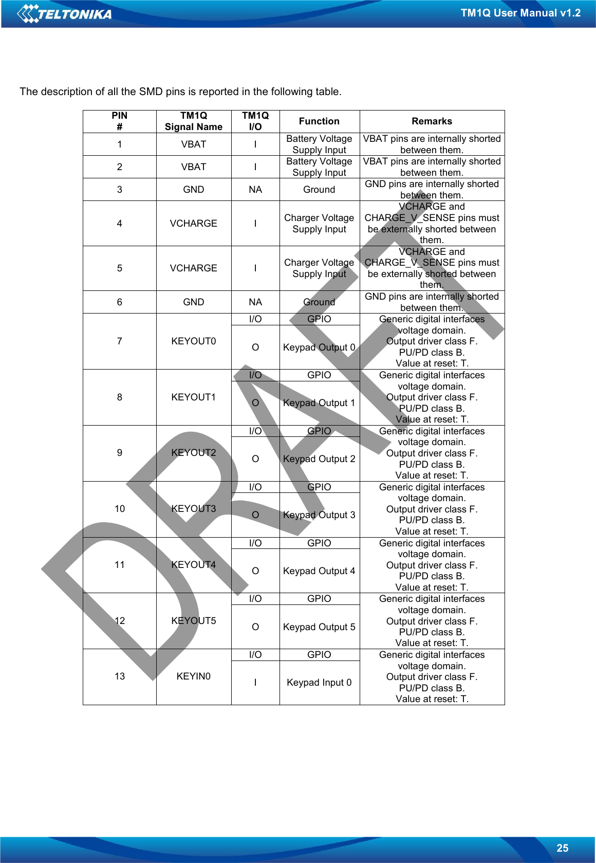
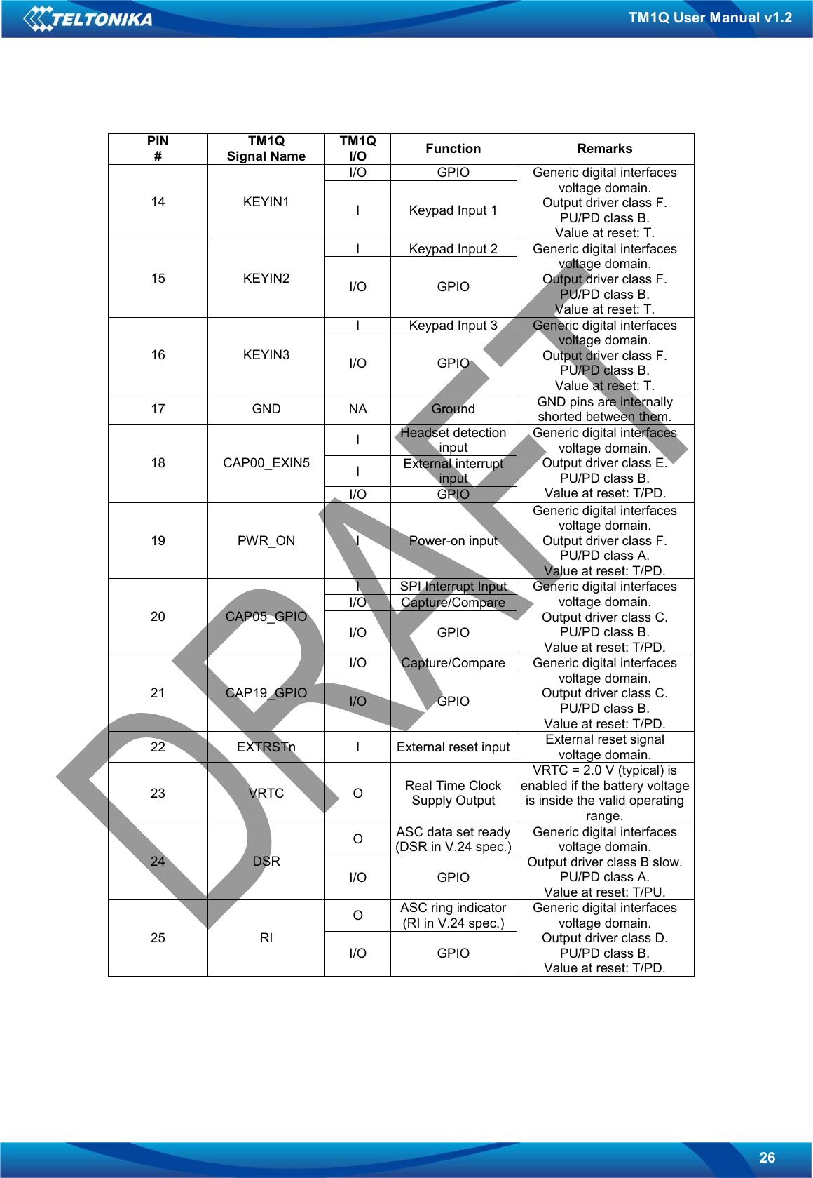
![21 TM1Q User Manual v1.2 5.2.4 Power saving Power saving is a special function that allows the reducing of power consumption during the idle time. If the clock increases, required power increases too. Therefore a solution for minimizing the power is the reducing of the master clock frequency when there aren’t activities. In this period the system doesn’t work with a clock of 26 MHz (“fast clock”) but with a clock of 32 kHz (RTC clock or “slow clock”). This switching between 26 MHz and 32 kHz clock is performed by SCCU (Standby Clock Control Unit) integrated in the baseband chipset. When the module is registered or attached to a network and a voice or data call is not enabled, it has to monitor periodically the paging channel of the current base station (paging block reception), as every mobile station, according to the GSM system specifications and requirements. In between, the module switches over to a power saving mode, discontinuous reception (DRX). The module processor core is activated during the paging block reception, so the module switches automatically its master clock frequency from the 32 kHz used in the power saving mode to the 26 MHz used in the active mode. The time period from two paging block receptions is defined by the network. If the module is registered to a network, the time interval between two paging block receptions can be set from 470.76 ms up to 2118.42 ms. Main priorities of power saving are the following: 1. Reduce base (min) current consumption; 2. Minimize full-speed running periods, minimize power saving on/off switching; 3. Reduce max current consumption. These points are reported in the following figure: Figure 5-2-2: Module current consumption profile in GSM idle (DRX-5) with power saving priorities highlighted More details related to the power saving and the serial port are described in the document [I.2]. This functionality can be disabled by the user through an AT command (more details on the document [I.1]). 12331233](https://usermanual.wiki/UAB-Teltonika/GM12TLTK5/User-Guide-1200661-Page-21.png)
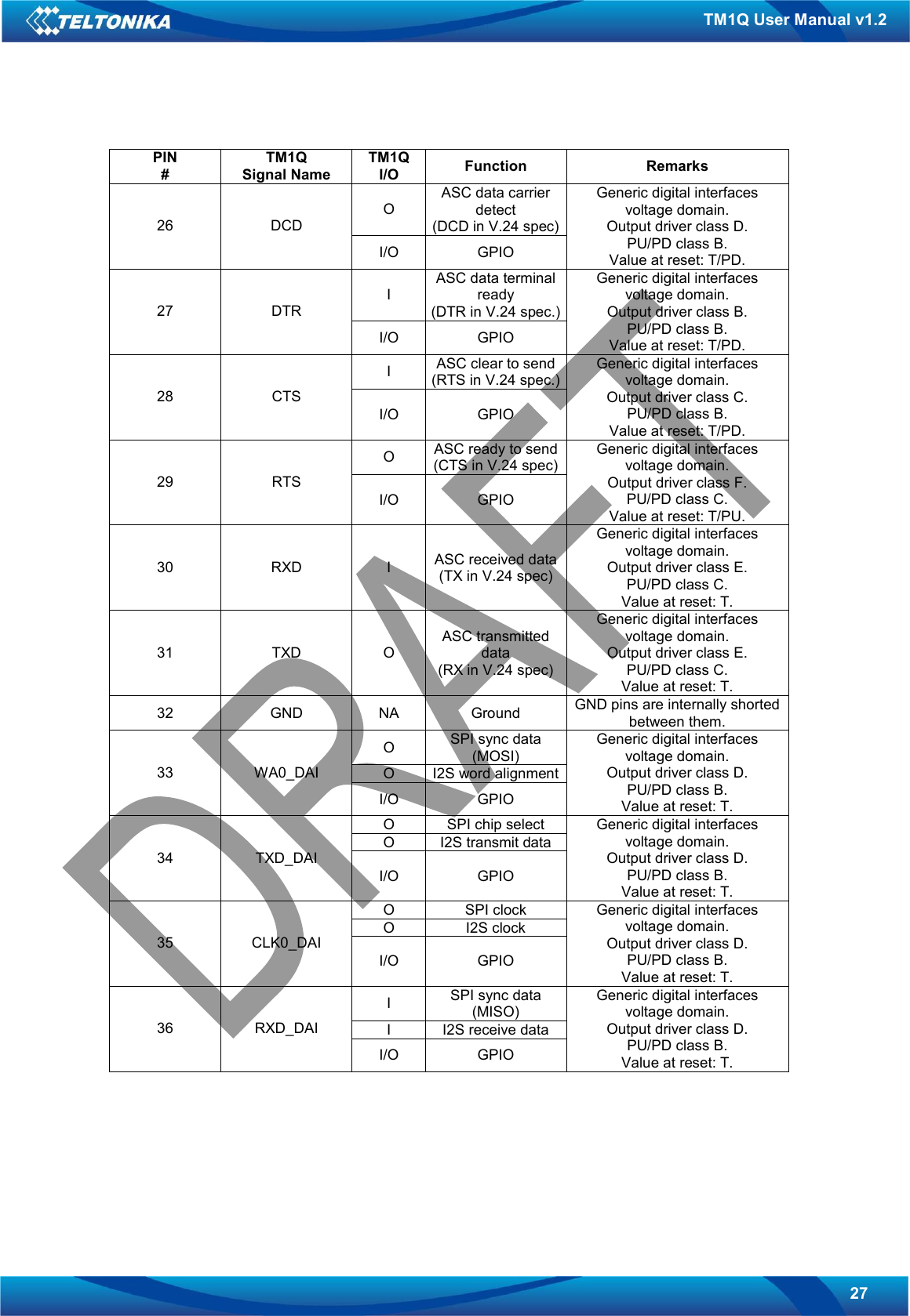
![36 TM1Q User Manual v1.2 6.7 Asynchronous serial interface (ASC) The asynchronous serial interface (ASC) relies on the Asynchronous Serial Controller hardware block provided by the baseband core. ASC features are: • Complete 9-pin serial port in compliance with the ITU V.24 specifications [E.1] (i.e. a complete RS-232 low voltage interface with hardware flow control is available); • The maximum data rate is 921600 bps for software download; • Intermediate data rates can be 2400, 4800, 9600, 19200, 38400, 57600, 115200, 230400, 460800 bps with No/Even/Odd parity, 7 or 8 bit frame length; • Power saving CTS indication available at the interface (see [I.2]). Software services available at ASC: • AT interface in compliance with GSM 27.007 [E.2]: the default speed for the AT interface is 115200 bps, the maximum speed is 230400 bps (see [I.1]); • MUX protocol available in compliance with GMS 27.010 [E.3]; • TELTONIKA_M2M software can be configured to access this port for customer specific usage. The serial port is limited to 921600 bps due to the FTDI level translator (serial to USB converter) of the motherboard. A more detailed description regarding software services and serial port behavior of the module is provided by the Teltonika document [I.2]. This is the ITU V.24 signals naming convention [E.1]: the module is a Data Communication Equipment (DCE), which is a modem; the external host processor or the PC is the Data Terminal Equipment (DTE). ITU V.24 conventional directions are in the previous figure like circuits numbers; please note that the hardware names of the module pins do not necessary reveal the ITU V.24 functionality. To download the code, only the two data lines (TXD and RXD) can be used. The other lines (CTS, RTS, DSR, RI, DCD and DTR) can be configured as GPIO. DTE / ComputerDCE / ModemTX (103) RX (104) RTS (105) CTS (106) DTR (108/2) DSR (107) DCD (109) RI (126)](https://usermanual.wiki/UAB-Teltonika/GM12TLTK5/User-Guide-1200661-Page-36.png)