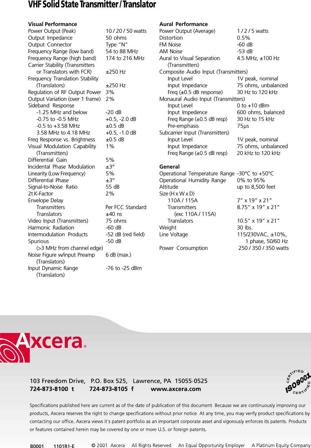
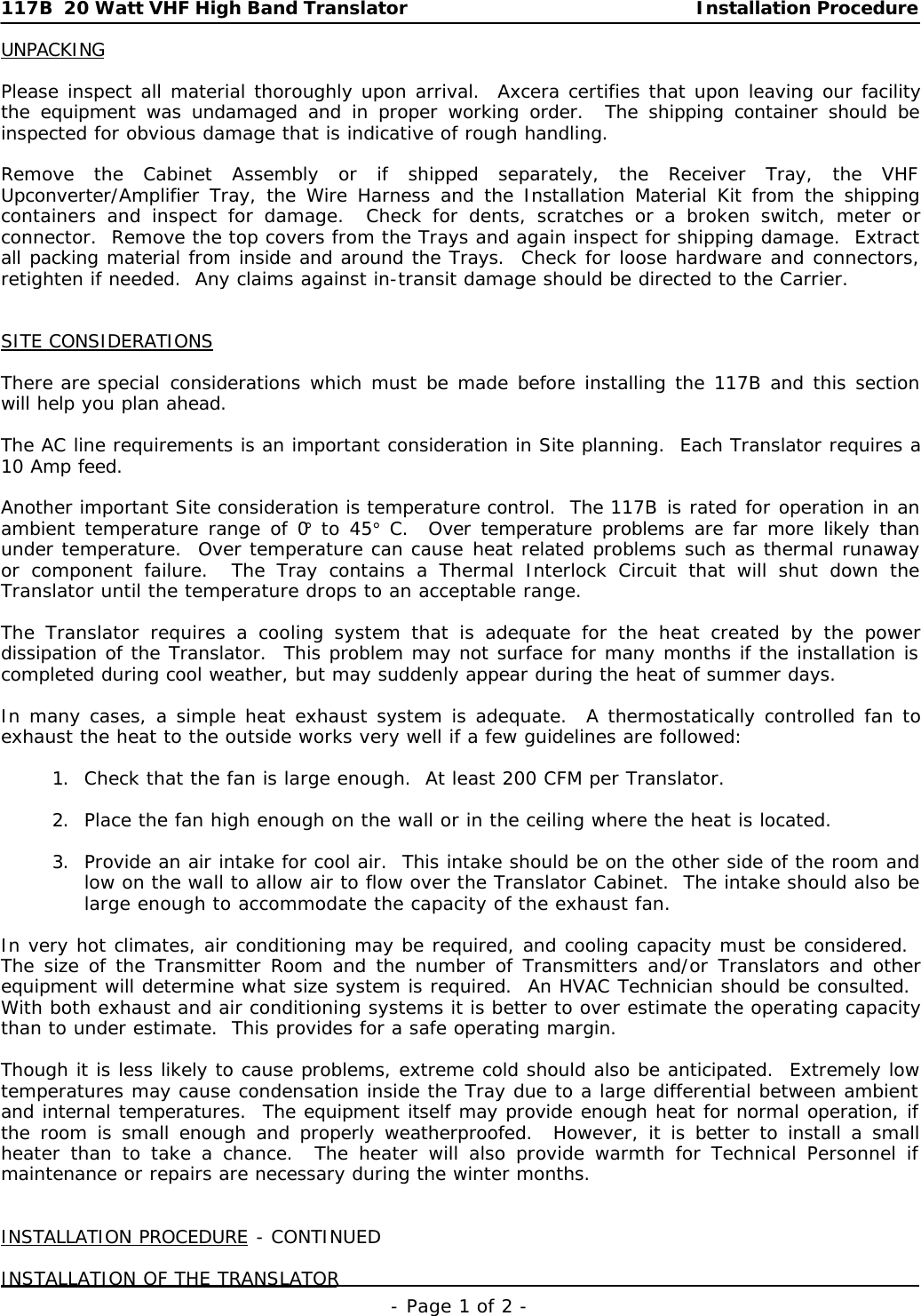
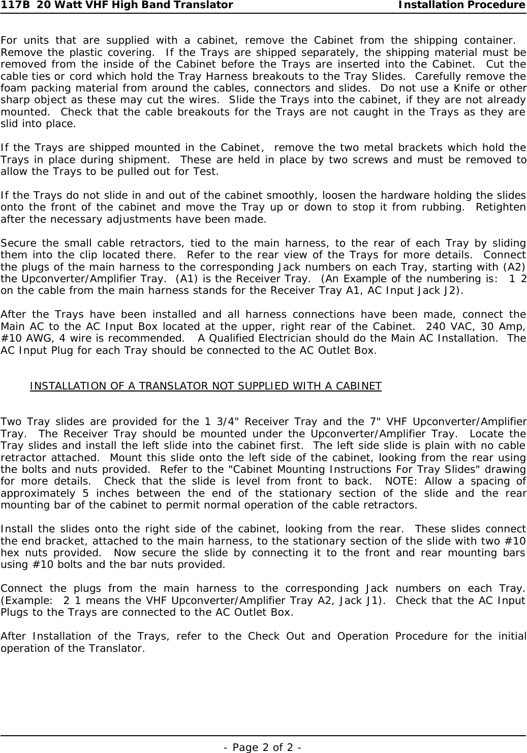
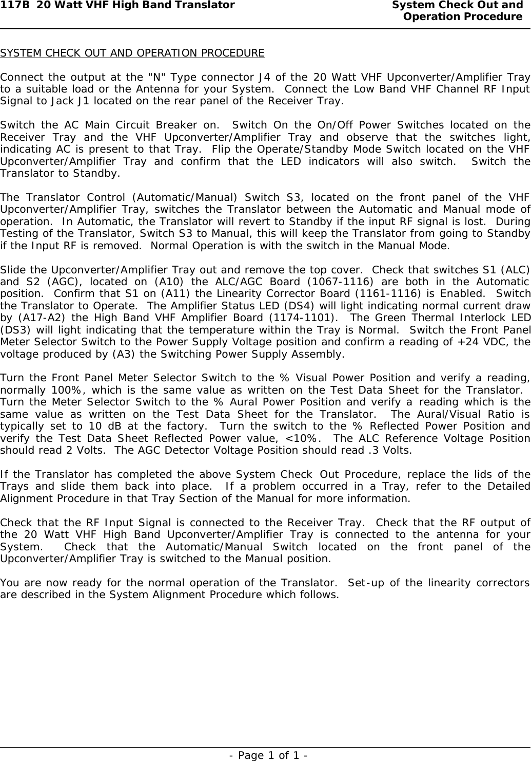
UBS Axcera 117B 20-Watt VHF High-band Translator User Manual 117B

UBS-Axcera 20-Watt VHF High-band Translator 117B

Axcera 117B Compiled User Manual

INSTRUCTION MANUAL117B20 WATT VHF HIGH BANDTRANSLATORAXCERA, LLC103 FREEDOM DRIVE P.O. BOX 525  LAWRENCE, PA 15055-0525 USA(724) 873-8100 • FAX (724) 873-8105www.axcera.com • info@axcera.com
117B 20 Watt VHF High Band Translator Table of Contents- Page 1 of 1 -Table of Contents1. Introduction:2. System – 117B: .................................................................................... 1175-1000a. System Descriptionb. Specificationsc. Installation Procedured. System Check Out and Operation Proceduree. Switch Position and Status for Normal Operationf. System Alignment Procedureg. Remote Control Interface Connectionsh. Drawings:1. Block Diagram.......................................................................... 1175-30002. Interconnect........................................................................... 1175-80003. VHF Low Band Receiver Tray:a. Circuit Descriptionb. Detailed Alignment Procedurec. Drawings:1. Block Diagram.......................................................................... 1265-31002. Interconnect........................................................................... 1265-81004. 20 Watt VHF High Band Upconverter/Amplifier Tray:a. Circuit Descriptionb. Detailed Alignment Procedurec. Drawings:1. Block Diagram.......................................................................... 1174-31002. Interconnect........................................................................... 1174-81005. Subassemblies:Refer to the subassembly section for the schematics of the boards and subassemblies thatmake up the 117B.  A drawing list showing the order in which the drawings appear in thesubassembly section is found at the beginning of that section.6. Maintenance and Harnesses:This section contains information on proper operation and maintenance of the 117B.
117B 20 Watt VHF High Band Translator System DescriptionThe 117B is a 20 Watt High Band VHF Television Translator which operates at a nominal InternallyDiplexed output power of 20 Watts Peak Sync Visual with typically 2 Watts Aural at a -10 dBAural/Visual Ratio.Functionally, it is comprised of a VHF Low Band Receiver Tray (1265-1100) and a 20 Watt VHFHigh Band Upconverter/Amplifier Tray {1355-1010 (Low Band), 1355-1011 (Mid Band) or 1355-1012(High Band)}.The Receiver Tray receives the Low Band VHF Channel Input at Jack (J1) and converts it to anInternally Diplexed Visual + Aural IF Output (+0 dBm) at J4.  The Visual + Aural IF output of theReceiver Tray at J4 is fed to J2 the IF Input Jack for the 20 Watt VHF High BandUpconverter/Amplifier Tray.  The Upconverter Section of the Tray mixes the IF with an internallygenerated L.O. to produce the VHF High Band Channel Frequency Output.  The signal is amplifiedand filtered in the Amplifier Section and directed to J4 the RF Output of the Tray.  This outputconnects to the Antenna for your System.Jack J7 located on the back of the Upconverter/Amplifier Tray is a 37 Position "D" Remote InterfaceConnector which provides the Operator with a connection for Remote Monitoring and Operation ofthe Translator.This manual provides the Technical Specifications of the Translator, along with the CircuitDescription, Alignment Procedure and the Schematics, Block Diagrams, Interconnects andReplacement Parts Lists necessary for the proper operation and maintenance of the 117B.
VHF Solid State Transmitter / Translator110A / 110B / 112B / 113B / 114B /115A / 115B / 117B / 118B / 119B■Completely Solid State■Designed for unattended operation withbuilt-in remote control interface■Small size – ideal where space is limited■Class A amplification up to 20W forexcellent linearity■Extensive front panel status and metering■Slide out tray assemblies for ease ofmaintenance with no extenders■BTSC Stereo Ready
VHF Solid State Transmitter / TranslatorVisual PerformancePower Output (Peak) 10 / 20 / 50 wattsOutput Impedance 50 ohmsOutput Connector Type “N”Frequency Range (low band) 54 to 88 MHzFrequency Range (high band) 174 to 216 MHzCarrier Stability (Transmittersor Translators with FCR) ±250 HzFrequency Translation Stability(Translators) ±250 HzRegulation of RF Output Power 3%Output Variation (over 1 frame) 2%Sideband Response-1.25 MHz and below -20 dB-0.75 to -0.5 MHz +0.5, -2.0 dB-0.5 to +3.58 MHz ±0.5 dB3.58 MHz to 4.18 MHz +0.5, -1.0 dBFreq Response vs. Brightness ±0.5 dBVisual Modulation Capability 1%(Transmitters)Differential Gain 5%Incidental Phase Modulation ±3°Linearity (Low Frequency) 5%Differential Phase ±3°Signal-to-Noise Ratio 55 dB2t K-Factor 2%Envelope DelayTransmitters Per FCC StandardTranslators ±40 nsVideo Input (Transmitters) 75 ohmsHarmonic Radiation -60 dBIntermodulation  Products -52 dB (red field)Spurious -50 dB(>3 MHz from channel edge)Noise Figure w/input Preamp 6 dB (max.)(Translators)Input Dynamic Range -76 to -25 dBm(Translators)Aural PerformancePower Output (Average) 1 / 2 / 5 wattsDistortion 0.5%FM Noise -60 dBAM Noise -53 dBAural to Visual Separation 4.5 MHz, ±100 Hz(Transmitters)Composite Audio Input (Transmitters)Input Level 1V peak, nominalInput Impedance 75 ohms, unbalancedFreq (±0.5 dB response) 30 Hz to 120 kHzMonaural Audio Input (Transmitters)Input Level 0 to +10 dBmInput Impedence 600 ohms, balancedFreq Range (±0.5 dB resp) 30 Hz to 15 kHzPre-emphasis 75µsSubcarrier Input (Transmitters)Input Level 1V peak, nominalInput Impedance 75 ohms, unbalancedFreq Range (±0.5 dB resp) 20 kHz to 120 kHzGeneralOperational Temperature Range -30°C to +50°COperational Humidity Range 0% to 95%Altitude up to 8,500 feetSize (H x W x D)110A / 115A 7” x 19” x 21”Transmitters 8.75” x 19” x 21”     (exc 110A / 115A)Translators 10.5” x 19” x 21”Weight 30 lbs.Line Voltage 115/230VAC, ±10%,1 phase, 50/60 HzPower  Consumption  250 / 350 / 350 wattsB0001      1101R1-E
117B  20 Watt VHF High Band Translator Installation Procedure- Page 1 of 2 -UNPACKINGPlease inspect all material thoroughly upon arrival.  Axcera certifies that upon leaving our facilitythe equipment was undamaged and in proper working order.  The shipping container should beinspected for obvious damage that is indicative of rough handling.Remove the Cabinet Assembly or if shipped separately, the Receiver Tray, the VHFUpconverter/Amplifier Tray, the Wire Harness and the Installation Material Kit from the shippingcontainers and inspect for damage.  Check for dents, scratches or a broken switch, meter orconnector.  Remove the top covers from the Trays and again inspect for shipping damage.  Extractall packing material from inside and around the Trays.  Check for loose hardware and connectors,retighten if needed.  Any claims against in-transit damage should be directed to the Carrier.SITE CONSIDERATIONSThere are special considerations which must be made before installing the 117B and this sectionwill help you plan ahead.The AC line requirements is an important consideration in Site planning.  Each Translator requires a10 Amp feed.Another important Site consideration is temperature control.  The 117B is rated for operation in anambient temperature range of 0° to 45° C.  Over temperature problems are far more likely thanunder temperature.  Over temperature can cause heat related problems such as thermal runawayor component failure.  The Tray contains a Thermal Interlock Circuit that will shut down theTranslator until the temperature drops to an acceptable range.The Translator requires a cooling system that is adequate for the heat created by the powerdissipation of the Translator.  This problem may not surface for many months if the installation iscompleted during cool weather, but may suddenly appear during the heat of summer days.In many cases, a simple heat exhaust system is adequate.  A thermostatically controlled fan toexhaust the heat to the outside works very well if a few guidelines are followed:1. Check that the fan is large enough.  At least 200 CFM per Translator.2. Place the fan high enough on the wall or in the ceiling where the heat is located.3. Provide an air intake for cool air.  This intake should be on the other side of the room andlow on the wall to allow air to flow over the Translator Cabinet.  The intake should also belarge enough to accommodate the capacity of the exhaust fan.In very hot climates, air conditioning may be required, and cooling capacity must be considered. The size of the Transmitter Room and the number of Transmitters and/or Translators and otherequipment will determine what size system is required.  An HVAC Technician should be consulted. With both exhaust and air conditioning systems it is better to over estimate the operating capacitythan to under estimate.  This provides for a safe operating margin.Though it is less likely to cause problems, extreme cold should also be anticipated.  Extremely lowtemperatures may cause condensation inside the Tray due to a large differential between ambientand internal temperatures.  The equipment itself may provide enough heat for normal operation, ifthe room is small enough and properly weatherproofed.  However, it is better to install a smallheater than to take a chance.  The heater will also provide warmth for Technical Personnel ifmaintenance or repairs are necessary during the winter months.INSTALLATION PROCEDURE - CONTINUEDINSTALLATION OF THE TRANSLATOR
117B  20 Watt VHF High Band Translator Installation Procedure- Page 2 of 2 -For units that are supplied with a cabinet, remove the Cabinet from the shipping container. Remove the plastic covering.  If the Trays are shipped separately, the shipping material must beremoved from the inside of the Cabinet before the Trays are inserted into the Cabinet.  Cut thecable ties or cord which hold the Tray Harness breakouts to the Tray Slides.  Carefully remove thefoam packing material from around the cables, connectors and slides.  Do not use a Knife or othersharp object as these may cut the wires.  Slide the Trays into the cabinet, if they are not alreadymounted.  Check that the cable breakouts for the Trays are not caught in the Trays as they areslid into place.If the Trays are shipped mounted in the Cabinet,  remove the two metal brackets which hold theTrays in place during shipment.  These are held in place by two screws and must be removed toallow the Trays to be pulled out for Test. If the Trays do not slide in and out of the cabinet smoothly, loosen the hardware holding the slidesonto the front of the cabinet and move the Tray up or down to stop it from rubbing.  Retightenafter the necessary adjustments have been made.Secure the small cable retractors, tied to the main harness, to the rear of each Tray by slidingthem into the clip located there.  Refer to the rear view of the Trays for more details.  Connectthe plugs of the main harness to the corresponding Jack numbers on each Tray, starting with (A2)the Upconverter/Amplifier Tray.  (A1) is the Receiver Tray.  (An Example of the numbering is:  1 2on the cable from the main harness stands for the Receiver Tray A1, AC Input Jack J2).After the Trays have been installed and all harness connections have been made, connect theMain AC to the AC Input Box located at the upper, right rear of the Cabinet.  240 VAC, 30 Amp,#10 AWG, 4 wire is recommended.   A Qualified Electrician should do the Main AC Installation.  TheAC Input Plug for each Tray should be connected to the AC Outlet Box.INSTALLATION OF A TRANSLATOR NOT SUPPLIED WITH A CABINETTwo Tray slides are provided for the 1 3/4" Receiver Tray and the 7" VHF Upconverter/AmplifierTray.  The Receiver Tray should be mounted under the Upconverter/Amplifier Tray.  Locate theTray slides and install the left slide into the cabinet first.  The left side slide is plain with no cableretractor attached.  Mount this slide onto the left side of the cabinet, looking from the rear usingthe bolts and nuts provided.  Refer to the "Cabinet Mounting Instructions For Tray Slides" drawingfor more details.  Check that the slide is level from front to back.  NOTE: Allow a spacing ofapproximately 5 inches between the end of the stationary section of the slide and the rearmounting bar of the cabinet to permit normal operation of the cable retractors.Install the slides onto the right side of the cabinet, looking from the rear.  These slides connectthe end bracket, attached to the main harness, to the stationary section of the slide with two #10hex nuts provided.  Now secure the slide by connecting it to the front and rear mounting barsusing #10 bolts and the bar nuts provided.Connect the plugs from the main harness to the corresponding Jack numbers on each Tray.(Example:  2 1 means the VHF Upconverter/Amplifier Tray A2, Jack J1).  Check that the AC InputPlugs to the Trays are connected to the AC Outlet Box.After Installation of the Trays, refer to the Check Out and Operation Procedure for the initialoperation of the Translator.
117B  20 Watt VHF High Band Translator  System Check Out andOperation Procedure- Page 1 of 1 -SYSTEM CHECK OUT AND OPERATION PROCEDUREConnect the output at the "N" Type connector J4 of the 20 Watt VHF Upconverter/Amplifier Trayto a suitable load or the Antenna for your System.  Connect the Low Band VHF Channel RF InputSignal to Jack J1 located on the rear panel of the Receiver Tray.Switch the AC Main Circuit Breaker on.  Switch On the On/Off Power Switches located on theReceiver Tray and the VHF Upconverter/Amplifier Tray and observe that the switches light,indicating AC is present to that Tray.  Flip the Operate/Standby Mode Switch located on the VHFUpconverter/Amplifier Tray and confirm that the LED indicators will also switch.  Switch theTranslator to Standby.The Translator Control (Automatic/Manual) Switch S3, located on the front panel of the VHFUpconverter/Amplifier Tray, switches the Translator between the Automatic and Manual mode ofoperation.  In Automatic, the Translator will revert to Standby if the input RF signal is lost.  DuringTesting of the Translator, Switch S3 to Manual, this will keep the Translator from going to Standbyif the Input RF is removed.  Normal Operation is with the switch in the Manual Mode.Slide the Upconverter/Amplifier Tray out and remove the top cover.  Check that switches S1 (ALC)and S2 (AGC), located on (A10) the ALC/AGC Board (1067-1116) are both in the Automaticposition.  Confirm that S1 on (A11) the Linearity Corrector Board (1161-1116) is Enabled.  Switchthe Translator to Operate.  The Amplifier Status LED (DS4) will light indicating normal current drawby (A17-A2) the High Band VHF Amplifier Board (1174-1101).  The Green Thermal Interlock LED(DS3) will light indicating that the temperature within the Tray is Normal.  Switch the Front PanelMeter Selector Switch to the Power Supply Voltage position and confirm a reading of +24 VDC, thevoltage produced by (A3) the Switching Power Supply Assembly.Turn the Front Panel Meter Selector Switch to the % Visual Power Position and verify a reading,normally 100%, which is the same value as written on the Test Data Sheet for the Translator. Turn the Meter Selector Switch to the % Aural Power Position and verify a reading which is thesame value as written on the Test Data Sheet for the Translator.  The Aural/Visual Ratio istypically set to 10 dB at the factory.  Turn the switch to the % Reflected Power Position andverify the Test Data Sheet Reflected Power value, <10%.  The ALC Reference Voltage Positionshould read 2 Volts.  The AGC Detector Voltage Position should read .3 Volts.If the Translator has completed the above System Check  Out Procedure, replace the lids of theTrays and slide them back into place.  If a problem occurred in a Tray, refer to the DetailedAlignment Procedure in that Tray Section of the Manual for more information.Check that the RF Input Signal is connected to the Receiver Tray.  Check that the RF output ofthe  20 Watt VHF High Band Upconverter/Amplifier Tray is connected to the antenna for yourSystem.  Check that the Automatic/Manual Switch located on the front panel of theUpconverter/Amplifier Tray is switched to the Manual position.You are now ready for the normal operation of the Translator.  Set-up of the linearity correctorsare described in the System Alignment Procedure which follows.
117B  20 Watt VHF High Band Translator Switch Position and Statusfor Normal Operation- Page 1 of 1 -Switch Position and Status for Normal OperationVHF Low Band Receiver Tray(A12) IF ALC Board (1109-1402) S1 switched to ALC position.20 WATT VHF High Band Upconverter/Amplifier Tray(A10) ALC/AGC Board (1067-1116) S1 switched to ALC positionS2 switched to AGC positionDS2 not lit (Video is Present)DS3 not lit (No ALC Fault)DS4 not lit (No AGC Fault)DS5 not lit (No RF Mute)(A11) Linearity Corrector Board (1161-1116) S1 switched to Correction in, Enable(A7) Transmitter Control Board (1161-1109) S1 switched to Modulator, DS5 lit.DS1 not lit (RF Input is present to theReceiver Tray).  May be lit all the time ifReceiver Tray not used.DS2 not lit (Video Input toUpconverter/Amplifier Tray is present).DS3 not lit (Video Input is present to theModulator Tray.  May be lit constantly ifOptional Modulator Tray not present.Front Panel Auto/Manual Switch (S3) Manual positionFront Panel Meter Selector Switch (S1) Selects metering: % Visual Output Power, %Aural Output Power, % Reflected Power,Power Supply Voltage, ALC Reference Voltageand AGC Detector Voltage.
117B  20 Watt VHF High Band Translator System Alignment Procedure- Page 1 of 2 -The Translator has been factory aligned and should not require adjustment to obtain normaloperation.  For a Detailed Alignment Procedure of each Tray, refer to the Receiver Tray or the 20Watt Upconverter/Amplifier Tray section of this Manual.SYSTEM SET UPThe system set-up includes adjustment of linearity to compensate for any amplifiers nonlinearresponses.  The Translator should be switched On initially into a 20 Watt dummy load to verify thatthe system is functioning properly.In the VHF Upconverter/Amplifier Tray, check that the ALC Auto/Manual  Switch (S1), located on(A10) the ALC/AGC Board (1067-1116), is in Auto.  Switch the On/Off Circuit Breakers located onthe front panels of the Receiver and the 20 Watt Upconverter/Amplifier to the On position.  Switchthe Translator to Operate and adjust the ALC Reference Pot (R47), or (R2) the Front Panel PowerAdjust, to obtain a Detected IF Output Voltage Level of +2.0 VDC at TP3 of the ALC/AGC Board. The Front Panel Meter in the ALC Reference Voltage position should also read +2.0 VDC.  Switchthe ALC Auto/Manual Switch (S1) to Manual ALC and adjust the Manual ALC Pot (R17) to obtain aDetected IF Output Voltage Level of +2.0 VDC at TP3 of the ALC/AGC Board.  Switch the ALCAuto/Manual Switch (S1) to Auto ALC.In the VHF Upconverter/Amplifier Tray, check that the AGC Switch (S2), located on (A10) theALC/AGC Board (1067-1116) is in Auto.  Preset the AGC Auto Gain Pot (R96) and the AGC ManualGain Pot (R101) to minimum (CCW).   Switch the Front Panel Automatic/Manual Switch to Manual. Switch the front panel Metering Switch, located on the 20 Watt Upconverter/Amplifier Tray, to the% Visual Output Power position and adjust the AGC Auto Gain pot (R96) located on (A10) theALC/AGC Board (1067-1116) to 100% on the meter.  Switch the AGC Switch (S2) to the ManualPosition and adjust the AGC Manual Gain pot (R101), located on the ALC/AGC Board, also for 100%on the meter.  Switch S2 back to Automatic.  The Front Panel Meter of the Upconverter/AmplifierTray in the AGC Detector Voltage position should read +.3 VDC, but the exact values are writtenon the Final Test Data Sheet for your System.Connect a Demodulator and Oscilloscope or other monitoring equipment to monitor the differentialgain and differential phase of the output signal.  If a synchronous demodulator having a quadraturevideo output is available, it may be employed with an X-Y Oscilloscope to display incidental carrierphase modulation (ICPM).  As shipped, the Translator was preset to include linearity (gain vs.level) predistortion which was adjusted to compensate for the corresponding non-linear distortionsof the solid state amplifier devices in the Translator.  Switch S1 located on (A11) the LinearityCorrector Board (1161-1116), to the On position.SYSTEM SET UP OF LINEARITYThe IF linearity correction function consists of three non-linear cascaded stages, each having anadjustable magnitude and a threshold, cut-in point.  The threshold adjustment determines at whatIF signal level the corresponding corrector stage begins to increase gain.  The magnitudeadjustment determines the amount of gain change for the part of the signal which exceeds thecorresponding threshold point.  Because the stages are cascaded, the order of correction isimportant.The first stage should cut-in nearest the white level, with the cut-in point of the second stagemoving toward black, with the last stage primarily stretching sync.  Linearity Corrector Board potsR3, R13 and R23 control the overall gain of each stage.  They were preset during Final Test at theFactory and should not require adjustment.  If moved accidentally, typical settings are R3, R13 andR23 mid-range.SYSTEM SET UP OF LINEARITY - CONTINUED
117B  20 Watt VHF High Band Translator System Alignment Procedure- Page 2 of 2 -To adjust the linearity correction from scratch, preset the Linearity Corrector pots R5, R16 and R26(threshold) to CCW and Linearity Corrector pots R2, R11 and R22 (magnitudes) CW.  Insert a 3.58MHz modulated staircase or ramp video test signal into the Tray and monitor the differential gain ofthe output.  Switch the ALC Auto/Manual Switch (S1) located on (A10) the ALC/AGC Board toAuto ALC.  This completes the ALC loop.Adjust the ALC Reference Pot (R47), or the Front Panel Power Adjust, to obtain a Detected IFOutput Voltage Level of +2.0 VDC at TP3 of the ALC/AGC Board.  The Front Panel Meter in the ALCReference Voltage position should also read +2.0 VDC.  Switch the ALC Auto/Manual Switch (S1)located on (A10) the ALC/AGC Board to Manual ALC and adjust the Manual ALC Pot (R17) to obtaina Detected IF Output Voltage Level of +2.0 VDC at TP3 of the ALC/AGC Board.  Switch the ALCAuto/Manual Switch (S1) located on (A10) the ALC/AGC Board to Auto ALC.  The ALC will nowoperate to maintain the corresponding peak power level following the correctors.  Therefore, thelinearity adjustment procedure should be repeated to achieve the correct differential gainpredistortion.  A positive aspect of linearity adjustment with ALC and AGC enabled is that thecontrol movements will not affect peak power.  This completes the preset steps.While observing Differential Gain, adjust the first linearity stage and advance the Threshold #1Control (R5) CW to stretch the signal above the White and Mid-Luminance region.  Back off on thecorresponding Magnitude #1  Control (R2) as required.  Next, advance the Threshold #2 Control(R16) to stretch the Black and Sync levels, then back off on the Magnitude #2 Control (R11) asrequired.  Adjust the Threshold #3 Control (R26) to further stretch the Black and Sync levels. Back off on the corresponding Magnitude #3 Control (R22) as required.  Go back through the Whitethrough Black and Sync correctors to touch up the effects of ALC Level changes during theadjustment.  If the amplifier is being driven very close to saturation, it may not be possible to getenough Sync Stretch while maintaining a flat differential gain.  The IF linearity correctors, whenproperly adjusted, will provide excellent lower sideband suppression and minimum frequencyresponse change vs. level.  These results are achieved by generating  intermod  products whichcancel with those produced by the amplifier, an effect which is not possible with video correction.FINAL AGC ADJUSTMENTCheck that the ALC Voltage is set to +2.0 VDC at TP3.  Switch the front panel Metering Switch,located on the Front Panel of the VHF Upconverter/Amplifier Tray, to the % Visual Output Powerposition and adjust the AGC Auto Gain pot (R96) located on the ALC/AGC Board to 100% on themeter.  Switch the AGC Switch (S2) the Manual Position and adjust the AGC Manual Gain pot(R101), located on the ALC/AGC Board, also for 100% on the meter.  Switch S2 back to Automatic. The Front Panel Meter of the Upconverter/Amplifier Tray in the AGC Detector Voltage positionshould read (.3 VDC) and in the ALC Reference Voltage Position (2 VDC), but the exact values arewritten on the Final Test Data Sheet for your System.This completes the System Alignment Procedure for the 117B.
117B  20 Watt VHF High Band Translator Remote Control Connections- Page 1 of 1 -Remote Control Interface Jack (J7)  37 Position "D" ConnectorFunction Connector Interface TypeRmt Operate Command J7 Pin 1 Contact ClosureRmt Operate/Standby Rtn J7 Pin 2Rmt Standby Command J7 Pin 3 Contact ClosureRmt Operate Indicator J7 Pin 4 50mA Max. Current SinkRmt Operate Indicator Rtn J7 Pin 5Rmt Standby Indicator J7 Pin 6 50mA Max. Current SinkRmt Standby Indicator Rtn J7 Pin 7Rmt Aural Power Metering J7 Pin 8 1v Full Scale At 1kRmt Aural Pwr Metering Rtn J7 Pin 9 Source ResistanceRmt Reflected Power Mtring J7 Pin 10 1v Full Scale At 1kRmt Reflected Pwr Mtr Rtn  J7 Pin 11 Source ResistanceRmt Visual Power Mtring J7 Pin 12 1v Full Scale At 1kRmt Visual Power Mtring Rtn J7 Pin 13 Source ResistanceRmt Visual + Aural Pwr Mtr J7 Pin 14 1v Full Scale At 1kRmt Vis + Aural Pwr Mtr Rtn J7 Pin 15 Source ResistanceRmt Am I.D. Indicator J7 Pin 20 50ma Max. Current SinkRmt Am I.D. Indicator Rtn J7 Pin 21Notes: These functions are accessed through the 37 position "D" connector (J7) located on therear panel of the VHF High Band Upconverter/Amplifier Tray.J7 Pins 16 - 19 are not used in this Translator.
117B  20 Watt VHF High Band Translator  UHF/VHF Receiver Tray,w/(Opt) Frequency CorrectionCircuit Description- Page 1 of 3 -The UHF/VHF Receiver Tray w/(Optional) Frequency Correction selects the desired UHF or VHF OnChannel Input Signal and converts it to a Combined IF Signal of 45.75 MHz Visual + 41.25 MHzAural.  The Tray also has provisions for a Frequency Correction Option that consists of a VCXOChannel Oscillator Assembly with a PLL Circuit which maintains an exact IF Output Frequency, overthe capture range of the PLL circuit, even if the Input UHF or VHF Frequency may vary.RF Input Signal PathThe RF Input to the Tray, (-61 dBm to -16 dBm in Level), is fed through J1 for 50Ω to (A7) theinput 50Ω Filter, DC Multiplexed (1035-1204 UHF, 1035-1902 VHF LB or 2065-1024 VHF HB) orthrough J5 for 75Ω to (A7) the 75Ω input Filter, DC Multiplexed (1035-1207 UHF, 1035-1903 VHFLB or 2065-1023 VHF HB), which is of a double tuned design that is adjusted to the desired InputUHF or VHF Channel Frequency.  Note: If the input signal is greater then -25dBm, an attenuatorshould be used to limit the level to -25dBm.  +12 VDC, for use by an (Optional) externalPreamplifier Assembly, connects to the filter through F1 a 1 Amp Fuse.  This +12 VDC is DCMultiplexed onto the input signal cable from the Preamplifier.  DS1 a Red LED located on TB1 in theTray will be lit if the +12 VDC is present on the input cable.  If a Preamplifier is not used, F1 shouldbe removed and DS1 should not be lit.The signal is next amplified +12 dB to approximately the -49 to -4 dBm level by a low noiseamplifier located on (A8-A1) the Dual Stage Amplifier Board (1227-1501) that is contained in (A8)the Dual Stage Amplifier Assembly (1227-1503).  The board has approximately +13 dB or +26 dB ofgain, depending on whether Jumper W1 on J5 is in place.  The signal is then filtered in (A9) aChannel Filter (1007-1101 UHF, 1034-1202 VHF LB or 2065-1000 VHF HB) and then applied back to(A8-A1) the Dual Stage Board where the same amplification takes place.  Jumper W1 on J7,located on the Dual Stage Board, should be removed if the Receiver Input level is greater than -40dBm.  The output is connected to (A10) the Downconverter Amplifier Assembly (1227-1505) thatcontains (A10-A1) the Downconverter Amplifier Board (1227-1502).  The RF, at the -47 dBm to -2dBm Level, connects to the "R" Input Jack of the Mixer Z1 located on the Downconverter AmplifierBoard.Local Oscillator Signal PathThe Local Oscillator Signal is derived from a cut to channel crystal mounted in an oven that isfactory set at 45° C.  The Oscillator operates at 1/8 for UHF, 1/4 for VHF High Band or 1/2 for VHFLow Band of the desired local oscillator frequency.  The crystal is mounted on (A4-A1) the ChannelOscillator Board, Dual Oven (1145-1201), that is part of the Channel Oscillator Assembly (1145-1202).  The oscillator circuitry is a modified Colpitts design operating in a separate oven set at 50°C. for improved stability.  If the Frequency Correction Option is purchased, the VCXO ChannelOscillator Assembly (1145-1206), which contains the VCXO Channel Oscillator Board (1145-1204),is used in place of the standard Channel Oscillator Assembly, and an AFC voltage from the PLLcircuit maintains the frequency of the VCXO.The output of the Channel Oscillator is connected to the (A5-A1) the x8 Multiplier Board(1227-1002) for UHF, the x4 Multiplier Board (1227-1525) for VHF HB or the x2 Multiplier Board(1227-1524) for VHF LB, which is located in (A5) the Multiplier Enclosure (1265-1125).  The propermultiplier board takes the output of the Channel Oscillator (+3 dBm) and multiplies it eight, four ortwo times by a series of three, two or one x2 Broadband Doublers (2x2x2 = x8), which producesthe L.O. signal on the desired frequency needed for the upconversion process.  The signal is thenamplified to the +16 dBm level.  A sample of the multiplied L.O. Signal is fed to a detector circuitwhich lights the Green LED DS1 that indicates that the L.O. is present at the Output Jack J2 of theMultiplier Board.  This Green LED is seen through a hole the lid of the Multiplier Assembly and is anindication, when lit, that there is a signal present at the output of the Multiplier Board.  The L.O.signal is filtered in (A6) a L.O. Filter 1007-1101 UHF, 2065-1000 VHF HB or 1034-1211 VHF LB) andthen sent (+15 dBm) to J2 on (A10-A1) the Downconverter Amplifier Board.  The L.O. Input to theDownconverter Amplifier Board is connected thru a 3 dB matching pad to the "L" Input of the Mixer(Z1) at a +12 dBm level.
117B  20 Watt VHF High Band Translator  UHF/VHF Receiver Tray,w/(Opt) Frequency CorrectionCircuit Description- Page 2 of 3 -Combined IF Signal PathThe L.O. and the RF signals are mixed in the Mixer Stage of the Downconverter Amplifier Board toproduce the desired IF difference frequency at -55 dBm to -10 dBm in level, depending on the RFInput Level.  The Combined IF Signal is routed to (A11-A1) the IF Filter/ALC Board (1227-1504),which is mounted in (A11) the IF Filter/ALC Enclosure (1265-1105).  The IF Filter/ALC Boardcontains a Pin Diode Attenuator circuit which is part of the Automatic Level Control (ALC) thatcontrols the level of the IF Signal to the two stage amplifier ICs U1 and U2.The (Optional) (A11-A2) SAW Filter/Amplifier Board (1035-1211) is also contained in the IFFilter/ALC Enclosure.  The SAW Filter/Amplifier Board connects to J5 and J6 of the IF Filter/ALCBoard if more attenuation of the Out Of Band products is needed.  If the SAW Filter/Amplifier Boardis not needed, a jumper connects the Combined IF from J5 to J6 on the IF Filter/ALC Board.The Combined IF is then bandpass filtered to the needed 6 MHz IF bandwidth around the 41.25MHz + 45.75 MHz Combined IF signal and amplified by U3 to the -41 dBm to +4 dBm Level before itis split.  One output is detected by U4 for use as the ALC reference level to the Pin DiodeAttenuator Circuit.  The ALC comparator drives the Pin Diode Attenuator Circuit to maintain thedesired output level, typically +2 dBm.  The other split output connects to J2 the Combined IFOutput of the board that is cabled to the IF Output Jack of the Tray at J4 (+2 dBm).Frequency Correction OptionIf the Frequency Correction Option (1227-1528) is purchased, (A13) the IF Filter/Limiter Board(1109-1001), (A14) the IF PLL Board (1109-1002), the (A15) IF Carrier Oven Oscillator Board(1100-1206), (A4) the VCXO Channel Oscillator Assembly (1145-1206) and (A16) an IF AmplifierBoard, High Gain (1197-1126) are part of the System.A Sample of the amplified and ALC controlled signal from the IF Filter/ALC Board is directed to theIF Amplifier Board, High Gain (1197-1126) where it is amplified and connected to J2 on (A13) the IFFilter/Limiter Board (1109-1001).  The IF is filtered by a SAW Filter, which passes Visual Carrier andAural Carrier only, and amplified before it is split.  The Aural IF Output is not used in this Tray.  Theother output of the splitter is amplified and applied to a Notch Filter.  The Notch Filter is tuned tothe Aural Frequency by C17 and R10 which reduces or eliminates the Aural IF from the Visual IFsignal.  The Visual IF Only signal then connects to a video detector circuit which in conjunctionwith U5 strips the video from the Visual IF signal.  The IF CW Signal is amplified and bufferedbefore it is connected to the output of the board at J6.  The IF CW connects to J2 of (A14) the IFPLL Board (1109-1002).The IF CW Signal (+3 dBm) on the IF PLL Board is wired to U1 a Divider IC which, in conjunctionwith U2, sets up one of the reference signals to the comparator circuit.  The other reference signalis derived from the 50 kHz reference Input at J4 which is a divided down 50 kHz sample of the 38.9MHz signal generated on (A15) the IF Carrier Oven Oscillator Board (1100-1206).  The 38.9 MHz IFCarrier Oven Oscillator Board is used instead of the 45.75 MHz IF Carrier Oven Oscillator Board tominimize the interference between the generated 45.75 MHz IF and the signal generated on the(A15) IF Carrier Oscillator Board.  The 38.9 MHz signal itself is not used, just the divided down 50kHz reference of the 38.9 MHz Signal is used.  The two reference signals applied to the IF PLLBoard are compared by U2 and a difference voltage (AFC) is produced.  The difference voltage(AFC), approximately -3 VDC, is fed from J3 of the board to FL2 of (A4) the VCXO Assembly.  Ifthe frequency of the VHF or UHF Input to the Tray should drift, the ALC voltage will change toincrease or decrease the output frequency of the VCXO Assembly which increases or decreasesthe L.O. Frequency that maintains the IF Frequency at the standard 45.75 + 41.25 MHzFrequency.  If the frequency of the Input Signal should drift out of the capture range of the PLLCircuit, DS1 the Red LED Unlock Indicator, located on the IF PLL Board, lights.Voltages for Operation of the Tray
117B  20 Watt VHF High Band Translator  UHF/VHF Receiver Tray,w/(Opt) Frequency CorrectionCircuit Description- Page 3 of 3 - January 7, 2002The AC input to the Tray is 117 VAC or 230 VAC and is directed thru Jack J2, of the (A1) PowerEntry Module (1265-1104), to the step down Toroid (A2).  The Power Entry Module contains anOn/Off Switch, a 4 Amp Slo-Blo Fuse and three MOVs which protect the Tray from transients orsurges which may occur on the AC Input Lines.  When the On/Off Switch is switched On, AC isapplied to the (A2) Toroid.  The Toroid steps down the voltage into two 16 VAC outputs which arefed to (A3) the +12V(3A)/-12V Power Supply Board (1092-1206).  The 16 VAC Inputs areconnected to the two full wave bridge networks one for +12 VDC and one for -12 VDC.  Theoutput of the +12 VDC rectifier is fed to three 7812 IC regulators (U1, U2 and U3) and the outputof the -12 VDC rectifier is fed to one 7912 IC regulator (U4).  The ±12V Power Supply Boardprovides the voltage regulated and current limited +12 VDC and -12 VDC to the rest of the boardsin the Tray.+12VDC for External Preamplifier+12 VDC is also applied through a 1 Amp Fuse F1 to (A7) the input DC Multiplexed UHF or VHFFilter.  The +12 VDC is multiplexed in the Filter onto the input coaxial cable that connects from the(Optional) Remote Preamplifier Unit to the Receiver Tray.  This supplies the Preamplifier with the+12 VDC needed for operation.  The Red LED DS1 mounted on the Terminal Block TB1 will be lit ifthe +12 VDC is applied to the coaxial cable.  Note: If the Red LED, DS1, is lit, the +12 VDC maydamage Test Equipment that is connected to the input of the Receiver Tray.  If a PreamplifierAssembly is not part of your System, F1 should be removed, therefore DS1 should not be lit andthe +12 VDC is not multiplexed onto the input coaxial cable.  A spare Fuse for F1 is supplied andstored near the fuse holder for F1.
117B  20 Watt VHF High Band Translator UHF/VHF Receiver Tray,w/(Optional) Frequency CorrectionDetailed Alignment Procedure- Page 1 of 4 -Connect a UHF or VHF Input with a Multiburst Test signal applied, that is at the desired ChannelFrequency, to J1 50Ω or J5 75Ω located on the rear of the (A3) VHF/UHF Receiver Tray.  Checkthat the On/Off Switch located on the rear of the Tray is On.Note: If the Red LED, DS1 is lit, +12 VDC is present at the input of the Receiver Tray and maydamage any test equipment connected to it.  Remove the fuse F1, DS1 will not be lit, beforeconnecting test equipment to the input jack of the Receiver Tray.(A7) UHF Filter, DC Multiplexed  (1035-1204, 50Ω or 1035-1207, 75Ω), VHF Filter, LB, DCMultiplexed  (1035-1902, 50Ω or 1035-1903, 75Ω) or VHF Filter, HB, DC Multiplexed  (2065-1024,50Ω or 2065-1023, 75Ω)The input UHF or VHF signal (-61 dBm to -16 dBm) is fed to the filter which has been factoryswept for 6 MHz Bandwidth at the Channel frequency and should not be tuned in the field.  Theoutput of the filter is directed to the J1 input of (A8) the Dual Stage Amplifier Assembly.(A8-A1) Dual Stage Amplifier Board  (1227-1501) Mounted in: (A8) a Dual Stage Amplifier Assembly (1227-1503).The Dual Stage Amplifier Board has been factory set to the channel frequency and contains nocustomer tuning adjustments.  The board has approximately +13 dB or +26 dB of gain, dependingon whether Jumper W1 on J5 is in place.(A9) UHF Filter (1007-1101), VHF LB Filter (1034-1202) or VHF HB Filter (2065-1000)The UHF or VHF Filter has been factory swept for 6 MHz Bandwidth at the Channel Frequency andshould not be tuned in the field.  The output of the filter (-50 dBm to -5 dBm) is fed either throughthe additional amplifier stage on the Variable Gain Amplifier Board or to (A10-A1) theDownconverter/Filter Board.(A4) Channel Oscillator Assembly, Dual Oven  (1145-1202) Contains: The Channel Oscillator Board, Dual Oven  (1145-1201).1. Connect the main output of the Channel Oscillator (J1) to a spectrum analyzer, adjusted toview the crystal frequency, and peak the tuning capacitors C6 and C18 for maximum output. Then tune L2 and L4 for maximum output.  The output level should be approximately +5dBm and the Oven Temperature should be maintained at 50°C.If a spectrum analyzer is not available, connect a DVM to TP1 on the x8, x4 or x2 MultiplierBoard.  Tune capacitors C6 and C18 for maximum voltage at TP1.  Then tune L2 and L4 formaximum voltage at TP1.2. Connect the sample output of the Channel Oscillator at J2 to a suitable counter and tuneC11, Coarse Adjust, and C9, Fine Adjust, to the crystal frequency.  Do not re-peak C6, C18,L2 or L4 because this may change the output frequency.Note:While adjusting C9 and C11 to the crystal frequency the peak voltage monitored at TP1 ofthe Multiplier Board should not decrease.  If a decrease does occur a problem with thecrystal is likely.3. Reconnect the main output at J1 of the Channel Oscillator to the Input Jack J1 of theMultiplier Board.
117B  20 Watt VHF High Band Translator UHF/VHF Receiver Tray,w/(Optional) Frequency CorrectionDetailed Alignment Procedure- Page 2 of 4 -(A4) Channel Oscillator Assembly, Dual Oven  (1145-1202) - Continued Contains: The (A4-A1) Channel Oscillator Board, Dual Oven  (1145-1201).Note:If the Optional Frequency Correction Kit is purchased a VCXO Assembly (1145-1206),containing a VCXO Board (1145-1204), will be used instead of the standard ChannelOscillator Board.  The adjustment will be the same as above except that the frequency isadjusted by moving the Jumper W1 on Jack J6, located on the IF PLL Board (1109-1002), toPins 2 & 3, Fixed Bias, and adjusting R15 on the IF PLL Board for -3 VDC at FL2 of the VCXOAssembly.  Move the Jumper W1 on Jack J6 to between Pins 1 & 2, AFC.  Connect theOscillator Sample output, at (J2) of the Channel Oscillator or the Front Panel Sample Jack(J9), to a suitable Frequency Counter and tune C11, Coarse Adjust, to the desiredfrequency.  Do not re-peak C6, C18, L2 or L4 because it may change the output frequency.Reconnect the main output (J1) of the Channel Oscillator (+5 dBm) to the input (J1) of theMultiplier Board.  DS1 the Red Unlock Indicator, located on the IF PLL Board, should not belit.(A5-A1) x8 Multiplier Board (1227-1002), x4 Multiplier Board (1227-1525) or x2 Multiplier Board(1227-1524)  Mounted in (A5) a Multiplier Enclosure (1265-1125).During Normal operation, the Green LED DS1, which can be seen through the access hole in theEnclosure Assembly, will be lit to indicate that the L.O. is present at the output of the x8 MultiplierBoard.1. Connect a Spectrum Analyzer to the Output Jack (J2) of the board.2. Tune C4, C6, C10, C12, C18 and C20 on the x8 and the appropriate caps on the otherboards for maximum output.  Readjust all the Capacitors to minimize the seventh and theninth harmonics, they should be at least -30 dB down, without affecting the x8 MultiplierOutput.If a Spectrum Analyzer is not available a DC voltmeter can be used as follows but the harmonicfrequencies must be minimized to prevent interference with other Channels.1. While Monitoring each Test Point with a DC voltmeter, maximize the voltage by tuning theBroadband Multipliers in the following sequence.2. For x8 Multiplier Board: Monitor TP1 with a DVM and tune C4 for maximum. (Typical .6 VDC)Monitor TP2 and tune C6 and C10 for maximum. (Typical 1.2 VDC)Monitor TP3 and tune C12 and C18 for maximum. (Typical 2 VDC)Monitor TP4 and tune C20 for maximum.Re-peak C12 and C10 while monitoring TP4. (Typical 3.5 VDC)For x4 Multiplier: Monitor TP1 with a DVM and tune C4 for maximum. (Typical .6 VDC)Monitor TP2 and tune C6 and C10 for maximum. (Typical 1.2 VDC)Monitor TP3 and tune C12 for maximum.Re-peak C12 and C10 while monitoring TP3. (Typical 2 VDC)For x2 Multiplier: Monitor TP1 with a DVM and tune C4 for maximum. (Typical .6 VDC)Monitor TP2 and tune C6 for maximum.Re-peak C4 and C6 while monitoring TP2. (Typical 1.2 VDC)The Green LED DS1 should be lit which indicates that the L.O. is present at the Output Jack J2 ofthe Multiplier Board.  The output of the Multiplier at J2 is connected to (A6) a UHF or VHF Filter.
117B  20 Watt VHF High Band Translator UHF/VHF Receiver Tray,w/(Optional) Frequency CorrectionDetailed Alignment Procedure- Page 3 of 4 -(A6) UHF Filter (1007-1101), VHF LB Filter (1034-1211) or VHF HB Filter (2065-1000)This filter has been factory swept at the L.O. frequency and should not be tuned without properequipment.  The output of the filter (+15 dBm) is connected to J2 on (A10) theDownconverter/Filter Assembly.(A10-A1) Downconverter/Amplifier Board  (1227-1502)  Mounted in: The (A10) Downconverter/Amplifier Assembly (1227-1505).The Mixer contains no adjustments and has a L.O. input of approximately +12 dBm in level appliedto J2 and a -47 dBm to -2 dBm RF input applied to J1.  The output IF level at J3 will be -55 dBm to-10 dBm.1. Connect a Spectrum Analyzer to the Output Jack J3 and adjust L1, C2 and L3 for bestfrequency response.2. Adjust C8 and R3 to notch out the Aural IF Frequency.The IF output at J3 (-55 dBm to -10 dBm) is fed to the IF Filter/ALC Board.  If needed a 10 dB Padcan be added to the circuit by moving the jumpers on J4 and J5 to the In position.(A11-A1) IF Filter/ALC Board  (1227-1504) Mounted in: The (A11) IF Filter/ALC Enclosure (1265-1105).1. Check that Switch S1, located on the IF Filter/ALC Board, is in the Auto ALC and that theoutput of the Board at J2 is approximately 0 dBm Output, adjust R23 if needed.(Optional) (A11-A2) SAW Filter/Amplifier Board  (1035-1211) Mounted in: The (A11) IF Filter/ALC Enclosure (1265-1105).This board is used for additional adjacent Channel rejection only if needed and may not be part ofthe Tray.The board contains no tuning adjustments.  The Jumpers W1 and W2 on J4 and J5 are placed forAttenuator In or Attenuator Out as needed to give the same output level at J2 as was at J1.(A2) ±12V Power Supply Board  (1092-1206)This board contains no adjustments.Note:If the (Optional) Frequency Corrector Kit is part of the tray, perform the followingadjustments.  If the Frequency Corrector Kit is not part of the tray, the tray is aligned andready for normal operation.(Optional) (A15) IF Carrier Oscillator Board  (1100-1206)1. Monitor J3 with a Spectrum Analyzer and observe the 38.9 MHz Visual IF signal at +5 dBm.2. Connect a Frequency Counter to J2 on the board or to J9 on the Front Panel and adjust C17for 38.9 MHz.
117B  20 Watt VHF High Band Translator UHF/VHF Receiver Tray,w/(Optional) Frequency CorrectionDetailed Alignment Procedure- Page 4 of 4 - (Optional) (A15) IF Carrier Oscillator Board  (1100-1206) - Continued3. Connect a Frequency Counter to J1 and check for the 50 kHz signal.  Adjust C17, if needed,to attain the 50 kHz frequency.  Remove the Jack on J5.  DS2 the Unlock Indicator shouldlight.  Replace the Jack onto J5.(Optional) (A13) IF Filter/Limiter Board  (1109-1001)1. Monitor the Aural Notch Test Output of the board at J5 and move the Jumper W1 on Jack J4to between Pins 2 & 3, Test Position.  Adjust C17 to the Aural IF Frequency, then adjustR10 to eliminate or minimize the Aural IF signal.  Move the Jumper W1 on Jack J4 back tobetween Pins 1 & 2, Operate Position.2. Monitor the IF CW Output of the board at J6 with an Oscilloscope and adjust R12 and C21for maximum Video Signal or connect a Spectrum Analyzer, in Zero Span, to J6 and adjustR12 and C21 for Minimum Video Signal amplitude ripple on the displayed signal.3. Adjust R15 for +3 dBm or Maximum output level if +3 dBm cannot be attained.(Optional) (A14) IF PLL Board  (1109-1002)Check that the Red LED DS1, Unlock Indicator, located on the board is not lit.If DS1 is lit, follow the alignment procedure for setting up the VCXO Channel Oscillator using R9 onthe IF PLL Board to set up the AFC Voltage for the Frequency of the VCXO.  If it is still lit, checkthe 50 kHz reference output of the (A15) IF Carrier Oven Oscillator.  If needed, follow thealignment procedure for the IF Carrier Oven Oscillator Board.(Optional) (A16) IF Amplifier Board, High Gain  (1197-1126)This board contains no customer adjustments.  The amplified IF output from the IF Filter/ALC Boardconnects to the IF Filter Limiter Board.The Receiver Tray is now set up and ready for normal operation.
117B 20 Watt VHF High Band Translator        Upconverter/Amplifier TrayCircuit Description- Page 1 of 3 -The VHF Upconverter/Amplifier Tray takes the modulated Visual + Aural IF input from the Modulatoror Receiver Tray and mixes it with a generated L.O. to produce the desired VHF High Band ChannelFrequency output.  The Tray then amplifies the VHF signal to the 20 Watt peak of Sync VisualOutput power level.IF SIGNAL PATHThe input of the Upconverter/Amplifier Tray is a modulated Internally Diplexed IF signal.  The IFinput network for the Tray is a simple  bandpass filter located on (A10) the ALC/AGC Board(1067-1116) which eliminates harmonics on the input signal.  The signal is next adjusted in level bythe pin attenuator/ALC circuitry and sent to (A11) the Linearity Corrector Board (1161-1116).  TheLinearity Correctors compensate for the amplitude non-linearities of the final amplifiers by providingan opposite amplitude transfer function.  The shape of this transfer function is set by thepotentiometers located on this board.  The  corrector circuits can also be bypassed by theswitches located on the board.The output of the Linearity Corrector Board is sent back to the ALC/AGC Board where an AGCcircuit compares a detected sample of the IF with a detected sample of the RF Output and adjuststhe IF output to maintain a constant gain after the first sample point.  This corrects for anytemperature drift that may occur in the amplifier devices.  (A9) The AGC Control Board (1137-1201) provides adjustments of the AGC feedback from the Transmitter Control Board to the VSWRCutback circuit located on the Transmitter Control Board. The ALC and AGC controlled IF signal from J4 on the board is fed to Jack (J2) located on (A16) theMixer/Amplifier Enclosure, which contains (A16-A1) a Filter/Mixer Board and (A16-A2) aFilter/Amplifier Board.  The IF Signal (-3 dBm Visual -13 dBm Aural) connects to Jack J7 of (A16-A1) the Filter/Mixer Board (1150-1102) and is wired to the Mixer stage Z1.  The Mixer mixes the IFwith the local oscillator  signal, that connects to J3 on the board, to produce the desired VHFoutput signal.L.O. SIGNAL PATHThe local oscillator signal is derived from a cut to channel crystal, located in an oven set at 45° C. This oscillator circuit, which is part of (A14-A1) the Channel Oscillator Board (1145-1201), is amodified  Colpitts circuit.  The Channel Oscillator Board is mounted in (A14) a Channel OscillatorAssembly (1145-1202) that has a separate oven set at 50° C for improved stability.  The output ofthe Oscillator Assembly at J1 is fed to (A15) a x4 Multiplier Board (1174-1112).  The x4 Multipliercontains two doubler circuits which multiply the L.O. signal to the required frequency needed formixing with the IF to produce the VHF High Band Channel Frequency.  The L.O. Signal (+5  dBm)from J2 on the board is connected Jack J1 of (A16) the Mixer/Amplifier Enclosure which is cabled toJack (J3) of (A16-A1) the VHF Filter/Mixer Board (1150-1102).  The L.O. Signal is amplified by U2and connected to J4 of the Board.  The amplified L.O. Signal at (+14 dBm) is jumpered to (J5) theL.O. Input Jack to the Mixer Z1.RF SIGNAL PATHThe L.O. input and the IF input are mixed to produce an output of the Mixer at Jack (J6) (-14 dBm)which contains the unwanted Mixer products along with the desired VHF Channel signal.  Thesesignals are jumpered from J6 to J1 the RF Input Jack of the VHF Filter/Mixer Board.RF SIGNAL PATH - CONTINUED
117B 20 Watt VHF High Band Translator        Upconverter/Amplifier TrayCircuit Description- Page 2 of 3 -The RF Signal is bandpass filtered for the desired VHF Channel frequency and then amplified by U1(-2 dBm Visual -12 dBm Aural) before it is connected to the RF Output Jack (J2) of the Board.  TheVHF output is connected to J7 of (A16-A2) the VHF Filter/Amplifier Board (1150-1101) on which itis filtered again and jumpered from J6 to J1 on the board.  The +12 VDC needed for operation ofthe Filter/Mixer Board and the Filter/Amplifier Board are provided by (A6) the +12V(3A)/-12V PowerSupply Board (1092-1206).  The filtered VHF is amplified to +8 dBm and -2 dBm, R9 sets the gainof the Filter/Amplifier Board using a Pin-Attenuator circuit, and connected to J2 the RF Output ofthe Board.J2 is cabled to J3 on the Mixer/Amplifier Enclosure Assembly.  The RF is connected to Jack (J1) on(A17-A1) the VHF High Band Driver Board (1174-1107).  The Driver Board contains a dual transistorstage Q1 that produces an output of +26 dBm Visual +16 dBm Aural.  (A17-A1) The VHF High BandDriver Board and (A17-A2) the VHF High Band Amplifier Board are mounted on (A17) the AmplifierHeatsink Assembly (1174-1111).  The output of the Driver Board connects to J1 of (A17-A2) theVHF High Band Amplifier Board (1174-1101).  The VHF High Band Amplifier Board contains a dualTransistor Stage that amplifies the VHF Signal to +44 dBm Visual and +34 dBm Aural.  R5 and R9 onthe board are Bias Adjustments which set the gain of the Board.  The VHF High Band Driver Boardand the High Band VHF Amplifier Board receive their +26 VDC Bias voltage from (A3) the +26 VDCSwitching Power Supply.  DS4 the front panel mounted Amplifier Status LED, that is mountedacross J3-2 and J3-3 of the VHF High Band Amplifier Board, will light if the +26 VDC is present tothe board.  The +26 VDC is connected to the board through (F1) the 8 Amp Fuse.  The output ofthe VHF High Band Amplifier Board at J2 (+44 dBm Visual and +34 dBm Aural) is connected to (A18-A1) a Low Pass Filter Board (1174-1102, 1174-1103 or 1174-1104 depending on frequency) whichcontains a Low Pass Filter and a 2nd Harmonic Trap.  The filtered output is cabled to (A18-A2 &A3) two Trap Filter Boards (1174-1105 or 1174-1106 depending on frequency) each Board containstwo Trap Filter circuits.  The first Trap Filter circuit, containing C6 and C8, is tuned to -4.5 MHzwhile the second Trap Filter, containing C2 and C4, is tuned to +9 MHz.  The output of (A18-A3)Trap Filter Board connects to Jack (J1) of (A23) a High Band VHF Coupler Board (1141-1002).  TheVHF Channel Frequency Output of the Coupler at J2 is directed to the rear of the Tray, the RFOutput Jack (J4), (+43 dBm Visual and +33 dBm Aural).A Forward Output Power Sample at J3 and a Reflected Output Power Sample at J4 are provided bythe VHF Coupler.  The Forward Power Sample is sent to (A24) a Splitter Assembly which providestwo Forward Power Sample outputs that are connected to J1 and J2 on (A26) the Visual/AuralMetering Board (1161-1103).  The Visual + Aural Forward Sample at J1 enters the board which istuned to provide an Aural Only Output Sample at Jack J6 - Pin 1 that connects to the front panelmeter for monitoring.  The Visual + Aural Forward Power Sample at J2 enters the board which istuned to produce a Visual Only Output Sample at Jack J7 - Pin 1 that connects to the front panelmeter for monitoring.  The Reflected Sample from J4 of the VHF Coupler connects to J4 of theVisual/Aural Metering Board and provides a Reflected Output Sample at Jack J9 - Pin 1 thatconnects to the front panel meter for monitoring.SYSTEM CONTROL AND OPERATIONThe system control for the Translator consists of (A7) the Transmitter Control Board (1161-1109)which provides control of the System Operation and the monitoring of the Status of the Tray andthe System.  The board provides or removes the commands for operation of the System. Associated with the Transmitter Control Board are front panel  LEDs for monitoring of Operate(DS5)/Standby (DS6) and Auto (DS7)/Manual (DS8) Status, Thermal Interlock (DS3), VSWRCutback (DS2), Input Signal Loss (DS1) Status and the Amplifier Status (DS4) of the High BandVHF Amplifier Board.  If the Reflected Power Level increases above the set level of R44, the boardwill cutback the output Power Level.  The board also contains (S1) a Receiver/Modulator Switchthat must be switched tothe proper position depending on if the System is a Translator and contains a Receiver Tray or is aTransmitter and contains a Modulator Tray.  If the Receiver Tray is selected, DS4 will be lit and ifthe Modulator Tray is selected, DS5 will be lit.
117B 20 Watt VHF High Band Translator        Upconverter/Amplifier TrayCircuit Description- Page 3 of 3 -Also located on the front panel of the Tray is (CB1) the 7.5 Amp On/Off Circuit Breaker, whichdistributes AC to the two power supplies, the ±12 VDC and the +26 VDC, that are part of theTray.  The Front Panel Meter (A27) is able to be switched by S1 to read the % Visual OutputPower, % Aural Output Power, % Visual + Aural Reflected Power, the Switching Power SupplyVoltage, the ALC Reference Voltage or the AGC Detector Voltage.A Front Panel Gain Control (R2) provides an ALC adjust which sets the Output Power level of theTransmitter.The AC needed to operate the Tray connects to the IEC Connector (A1) located on the rear panel. The IEC Connector contains a 10 Amp over-current protection Fuse F1.  The AC connects to TB1which has jumpers for 115 or 230 VAC operation and MOV devices connected across the lines forsurge and spike protection.  The circuit breaker (CB1), which lights when switched on and AC ispresent to the Tray, controls the Input AC that connects to TB1.  When CB1 is switched On theinput AC connects to (A5) the step down Toroid for the ±12 VDC Power Supply.  The AC is alsoconnected to the contacts of the Isolation Relay (A2).  The Isolation Relay controls the ACVoltage that is supplied to the Switching Power Supply which is needed for operation.  TheIsolation Relay is energized by a Relay Enable Command from the Transmitter Control Board andoccurs when the System is switched to Operate and there is no Thermal Fault present.  TheTransmitter Control Board removes the Relay Enable Command to the Isolation Relay in the eventof excessive temperature sensed by the Thermal Switch (A17-A3) mounted to the AmplifierHeatsink Assembly.  The de-energized Isolation Relay removes the AC Input to the SwitchingPower Supply, which shuts down the power supply.POWER SUPPLIESThere are two power supplies in the Tray which provide the needed ±12 VDC and the +26 VDC forthe operation of the Tray and the Amplifier Boards.  The ±12 Volt Power Supply is comprised of(A5) an AC Step-Down Toroid and (A6) a +12V(3A)/-12V Power Supply Board (1092-1206).  The+12V(3A)/-12V Power Supply Board contains two full wave bridge rectifier networks, one for +12VDC and one for -12 VDC.  The board contains three nonadjustable regulator IC circuits with shortcircuit protection (U1, U2 & U3) for +12 VDC and one nonadjustable regulator IC circuit with shortcircuit protection (U4) for -12 VDC.  The second power supply in the Tray is a +26 Volt SwitchingPower Supply Assembly (V250D04) that provides the +26 VDC to (A17-A1) the VHF High BandDriver Board and (A17-A2) the VHF High Band Amplifier Board.
117B  20 Watt VHF High Band Translator       Upconverter/Amplifier TrayDetailed Alignment Procedure- Page 1 of 5 -Use the IF Output of the Modulator or the Receiver Tray to drive the VHF Upconverter/AmplifierTray.The Upconverter/Amplifier Tray includes adjustments for automatic level control (ALC) of the drivelevel, linearity (amplitude pre-distortion)  predistortion and the RF amplifier stages.  TheUpconverter/Amplifier Tray also includes adjustments for the local oscillator multiplier chain and thelocal oscillator center frequency.Switch the Front Panel mounted On/Off Upconverter/Amplifier Circuit Breaker to the On position. Switch the Auto/Manual Switch to the Manual position.  Switch the Operate/Standby Switch tothe Standby position.(A14) CHANNEL OSCILLATOR ASSEMBLY  (1145-1202) CONTAINS: (A14-A1) CHANNEL OSCILLATOR BOARD (1145-1201).1. Connect the main output of the Channel Oscillator (J1) to a spectrum analyzer, tuned tothe crystal frequency.  Switch the Operate/Standby Switch to Operate, and peak thetuning capacitors C6 and C18 for maximum output.  Tune L2 and L4 for maximum output. The output level should be approximately +5 dBm.2. If a spectrum analyzer is not available, connect a DVM to TP1 on the x4 Multiplier Board. Tune capacitors C6 and C18 for maximum  voltage, then tune L2 and L4 also for maximumvoltage output at TP1.3. Connect the sample output of the channel oscillator (J2) to a suitable counter and tuneC11, coarse adjustment, and C9, fine adjustment, to the crystal frequency.  DO NOTRE-PEAK C6, C18, L2 or L4, because it may change the output frequency.NOTE: While adjusting C9 and C11 to the crystal frequency the peak voltage monitored at TP1 ofthe x4 Multiplier Board should not decrease.  If a decrease does occur a problem may existwith the crystal.4. Reconnect the main output (J1) of the Channel Oscillator to the input (J1) of the x4Multiplier.(A15) x4 MULTIPLIER BOARD  (1174-1112)While monitoring with a DC voltmeter, maximize each test point voltage by tuning the broadbandmultipliers in sequence.1. Monitor TP1 with a DVM and Tune C4 for Maximum.Monitor TP2 with a DVM and Tune C6 and C10 for Maximum.Monitor TP3 with a DVM and Tune C12 then re-peak C4, C6 and C10 for Maximum.2. Connect a Spectrum Analyzer, tuned to 4 times the crystal frequency, to the x4 Multiplieroutput Jack (J2).  Monitor the output and peak the tuning capacitors for maximum output.The output of the x4 Multiplier connects to (A16-A1) the Filter/Mixer Board.(A16-A1) FILTER/MIXER BOARD  (1150-1102)1. Monitor J4 the L.O. Output of the Board with a Spectrum Analyzer and adjust C12 and C18for maximum output (+14 dBm) at the L.O. frequency.2. Adjust C13 and C17 for best frequency response for the L.O. frequency.
117B  20 Watt VHF High Band Translator       Upconverter/Amplifier TrayDetailed Alignment Procedure- Page 2 of 5 -PRESET THE FOLLOWING SWITCHES:(A10) ALC/AGC BoardS1 to ALC ManualS2 to AGC Manual(A11) Linearity Corrector BoardS1 to Off(A10) ALC/AGC BOARD  (1067-1116)The Input IF signal is cabled to (J1) IF input of the ALC/AGC Board.1. Remove the J1 plug from the board, observe that DS2, Input Fault, lights.  Reconnect J1and observe DS2 extinguished.2. Check that S1 is in Manual.  Monitor the output at J2 with a Spectrum Analyzer and adjustR17 for 0 dBm level.3. Insert a NTSC multiburst video test signal to the Modulator Tray and tune C2 for a flatfrequency response ±.5 dB.  Reconnect J2.  Jack (J2) of the board is cabled to the J1 InputJack of the Linearity Corrector Board.(A11) LINEARITY CORRECTOR BOARD  (1161-1116)Check that the linearity pre-correction (S1) is switched Out.1. Monitor the Output Connector (J2) of the Linearity Corrector Board and verify an IF outputof approximately 0 dBm level.No other adjustments are necessary to the linearity corrector at this point of the procedure.  TheIF output of the Linearity Corrector Board is fed back to the ALC/AGC Board at connector (J3).(A10) ALC/AGC BOARD  (1067-1116)1. Switch S1 on the ALC/AGC Board to ALC Auto.  This completes the ALC loop.2. The initial ALC IF adjustment consists of presetting the Front Panel Power Control Pot (R2)to Mid-Range and adjusting the ALC reference pot (R47) to obtain a detected IF outputlevel of +2 VDC at TP3 of the ALC/AGC Board.  Switch the Operate/Standby Switch to theOperate position.3. Remove the IF output plug (J4) from the ALC/AGC Board, and monitor the output from J4with a Spectrum Analyzer.  Adjust R101 for (-3 dBm pk Visual and -13 dBm Aural).4. Insert a NTSC multiburst video signal to the Input of the Modulator or to the Receiver Trayand tune C33 for a flat frequency response ±.5 dB.  Reconnect J4.The output from J4 is cabled to J2 the IF input of  (A16) the Mixer/Amplifier EnclosureAssembly which connects to J7 of (A16-A1) the Filter/Mixer Board.
117B  20 Watt VHF High Band Translator       Upconverter/Amplifier TrayDetailed Alignment Procedure- Page 3 of 5 -THE FOLLOWING DETAILS THE MEANING OF EACH LED ON THE ALC/AGC BOARD WHENILLUMINATED.DS2 -Abnormally low or no IF signal is present at the IF input connector J1.DS3 -Indicates that the ALC circuit is unable to maintain the signal level requested by the ALCreference.  Usually caused by excessive attenuation in the Linearity Corrector path orSwitch S1 is in Manual ALC.DS4 -Indicates that the AGC circuit is unable to maintain the signal level requested by the AGCreference.  Usually caused by excessive attenuation in the Amplifier Circuits or Switch S2 isin Manual AGC.DS5 -A Mute command is present.  Typically generated when the Translator is in Standby.(A16-A1) FILTER/MIXER BOARD (1150-1102)The L.O. signal and the IF signal are mixed to produce the desired channel frequency which is thedifference product of the two signals.  The output of the Mixer at J6 (-14 dBm) is jumpered to J1the input to a  bandpass filter located on the Board.  This filter has been factory swept andadjusted for a 6 MHz bandwidth and should not be tuned without proper equipment.The output of the Filter is amplified by U1 to (-2 dBm) and is fed to the Filter/Amplifier Board.(A16-A2) FILTER/AMPLIFIER BOARD  (1150-1101)The Filter/Amplifier Board has been factory swept and adjusted for a 6 MHz bandwidth and shouldnot be tuned without proper equipment.The filtered output connects to J1 of the board and is amplified by U1 to +8 dBm Visual and -2 dBmAural in level.  Adjust R9 for a Nominal output of +8 dBm Visual -2 dBm Aural.  The output is fed tothe VHF High Band Driver Board (A17-A1).(A17-A1) VHF HIGH BAND DRIVER BOARD  (1174-1107)This amplifier has a gain of about 18 dB and is tuned with C15 for maximum output at the VHFChannel Frequency.  The RF output (+26 dBm Visual and +16  dBm Aural) is fed to the VHF HighBand Amplifier Board (A17-A2).1. Adjust the operating static current to .6 Amps with R4 located on the Board.  This isaccomplished by adjusting R4 for 600 mA, .06 Volts across R6, a .1 Ohm/3 Watt Resistor.The RF output (+44 dBm Visual and +34 dBm Aural) is fed to the Amplifier Board. (A17-A2) VHF HIGH BAND AMPLIFIER BOARD  (1174-1101)The amplifier has a nominal gain of 18 dB and is tuned with C9 & C19 for maximum output.1. Adjust the operating static currents for Q1 to 2 Amps for each half of the device, 4 Ampstotal.  This is accomplished by presetting Pots R5 and R9 full CCW then adjusting R5 for a .2Volt, 200mV, drop across R21, a .1W/5W Resistor, located on the Amplifier Board.  Nextadjust R9 for .4 Volt, 400mV, drop across R21.  This gives the desired 4 Amps of StaticCurrent for the Q1 Device.
117B  20 Watt VHF High Band Translator       Upconverter/Amplifier TrayDetailed Alignment Procedure- Page 4 of 5 -The output of the Amplifier Board at J2 (+44 dBm Visual and +34 dBm Aural) is fed to the Low PassFilter Board.(A18-A1) LOW PASS FILTER BOARD  (1174-1102, 1174-1103 OR 1174-1104)The Low Pass Filter Board is adjusted at the factory and should not need to be adjusted in thefield.  The second part of the Board is a 2nd Harmonic Trap that is also factory adjusted andshould not be adjusted.The output of the Low Pass Filter Board at J2 is fed to a Trap Filter Board.(A18-A2 & A18-A3) TRAP FILTER BOARDS  (1174-1105 OR 1174-1106)The two Trap Filter Boards are adjusted at the factory and should not need to be adjusted in thefield.  Each board contains two Notch Circuits.  The Center Frequency of first notch, -4.5 MHz, isadjusted by C8, and the depth of the Notch is adjusted by C6.  The Center Frequency of secondnotch, +9 MHz, is adjusted by C4, and the depth of the Notch is adjusted by C2.  Both boards areadjusted the same.The output of the Trap Filter Board at J2 is fed to a High Band VHF Coupler Board.(A23) HIGH BAND VHF COUPLER BOARD  (1141-1002)Forward and Reflected power samples are taken from the VHF Coupler Board and the ReflectedSample is fed directly to the Visual/Aural Metering Board (A26).  The Forward sample is split by(A24) and fed to the Visual/Aural Metering Board (A26).The Output of the VHF Coupler Board (A23) is connected to the RF Output Jack (J4) of the Tray(+43 dBm Visual and +33 dBm Aural).(A26) VISUAL/AURAL METERING BOARD  (1161-1103)1. While monitoring the RF output of the Tray, adjust R101 on the ALC/AGC Board (A10), S2 inAGC Manual, for a reading of 20 Watts Peak Sync Power.2. Switch the Front Panel Meter AGC Detector Voltage Position and adjust R28 for .3 Volts.3. Switch the Front Panel Meter to the % Aural Output Power position and adjust C5 forMaximum Aural Output.4. Adjust R11 for a reading of 100% Aural Output on the Front Panel Meter.5. Remove the Aural by removing Jack J15 located on the Clamp/Modulator Board in theModulator Tray or by removing the Aural from the RF Input to the Receiver Tray.  Switchthe Front Panel Meter to the Visual Output Power position and adjust R29, located on theVisual/Aural Metering Board, for a reading of 100% on the front panel meter.6. Insert the Aural back into the System.  Adjust R39 for 100% Output in the Visual OutputPower position.Remove the cable now on J4 and move the cable from J1 to J4.  Switch the Meter Selector Switchto the % Reflected Power Position and adjust R47 for a reading of 100%.  Switch the cable from J4back to J1 and reconnect the cable to J4.
117B  20 Watt VHF High Band Translator       Upconverter/Amplifier TrayDetailed Alignment Procedure- Page 5 of 5 -(A7) TRANSMITTER CONTROL BOARD  (1161-1109)The adjustments on the Board were set at the factory and should not be realigned.(A9) AGC CONTROL BOARD  (1137-1201)The AGC Control Voltage is adjusted by R3 for 1 VDC at TP3. Switch S2 located on the ALC/AGC Board back to Automatic for normal operation and adjust R96for a reading of 100% in the Visual Output Power position.(A6) +12V(3A)/-12V POWER SUPPLY BOARD  (1092-1206)The Board contains no adjustments. (A3) +26 VDC SWITCHING POWER SUPPLY ASSEMBLY  (V250D04)The Assembly was factory adjusted for the proper voltage (+26 VDC) needed by the amplifierboards.  If the Switching Power Supply should shut down due to a problem in the Tray, after theproblem is repaired, the supply can be reset by turning the Tray Off, waiting a moment, thenturning it On again.This concludes the Detailed Alignment Procedure for the Upconverter/Amplifier Tray.For normal operation, the Auto/Manual Switch located on the front panel, should be in the Autoposition.  S1 and S2 located on the ALC/AGC Board should both be in the Auto Position.
117B 20 Watt VHF High Band Translator Drawing List (Subassemblies)- Page 1 of 2 -Drawing List (Subassemblies)±12V Power Supply BoardSchematic.................................................................................................. 1001-3009IF Filter/Amplifier BoardSchematic.................................................................................................. 1005-3205VHF Channel Filter, Low BandSchematic.................................................................................................. 1034-3202VHF L.O. Filter, Wide, 2 SectionSchematic.................................................................................................. 1034-3211VHF Mixer/Amplifier BoardSchematic.................................................................................................. 1035-3901ALC/AGC BoardSchematic.................................................................................................. 1067-3116+12V(3A)/-12V Power Supply BoardSchematic.................................................................................................. 1092-3206IF ALC Board, 45.75 MHzSchematic.................................................................................................. 1109-3402AGC Control BoardSchematic.................................................................................................. 1137-3201Channel Oscillator Board, Dual OvenSchematic.................................................................................................. 1145-3201VHF Filter/Amplifier BoardSchematic.................................................................................................. 1150-3101VHF Filter/Mixer BoardSchematic.................................................................................................. 1150-3102IF Filter Board, 45.75 MHzSchematic.................................................................................................. 1161-3007Visual/Aural Metering BoardSchematic.................................................................................................. 1161-3103Transmitter Control BoardSchematic.................................................................................................. 1161-3109Linearity Corrector BoardSchematic.................................................................................................. 1161-3116x2 Multiplier BoardSchematic.................................................................................................. 1172-3111VHF High Band Amplifier Board, +28V I/PSchematic.................................................................................................. 1174-3101
117B 20 Watt VHF High Band Translator Drawing List (Subassemblies)- Page 2 of 2 -VHF Low Pass Filter Board, 174-192 MHzSchematic.................................................................................................. 1174-3102VHF Low Pass Filter Board, 193-216 MHzSchematic.................................................................................................. 1174-3103VHF Low Pass Filter Board, 217-238 MHzSchematic.................................................................................................. 1174-3104VHF Trap Filter Board, 174-216 MHzSchematic.................................................................................................. 1174-3105VHF Trap Filter Board, 217-238 MHzSchematic.................................................................................................. 1174-3106VHF High Band Driver BoardSchematic.................................................................................................. 1174-3107x4 Multiplier BoardSchematic.................................................................................................. 1174-3112Downconverter Filter BoardSchematic.................................................................................................. 1227-3502Dual Stage Amplifier AssemblySchematic.................................................................................................. 1227-3501IF ALC BoardSchematic.................................................................................................. 1227-3504X2 Multiplier BoardSchematic.................................................................................................. 1227-3524+26V/250W Switching Power Supply, located in Upconverter/Amplifier Tray.....................V250D04
117B 20 Watt VHF High Band Translator MaintenanceThe 117B is designed with components that require little or no periodic maintenance except for the routine cleaningof the Trays.  The amount and time interval between cleanings depends on the conditions within the Transmitterroom.  The air flow through the cabinets will be lowered which could cause heat related problems if the fans in theCabinet are not cleaned.  Clean them with a vacuum cleaner to remove any foreign  material which may haveaccumulated. The individual Trays in the Translator must also be cleaned.  The amount and time interval between cleaningsdepends on the conditions within the Transmitter room.  While the electronics have been designed to function evenif covered with dust.  A heavy buildup of dust, dirt or insects will hinder the effectiveness of the cooling of thecomponents and lead to a thermal shutdown or premature failure of the affected Tray.When the front panels become  dust covered, the top covers should be removed and any accumulated foreignmaterial removed.  A vacuum cleaner utilizing a small wand type attachment is an excellent way to suction out thedirt.  Alcohol and other cleaning agents should not be used unless your certain that the solvents will not damagecomponents or the silk-screened markings on the Trays and boards.  Water based cleaners can be used, but donot saturate the components.  The fans and heatsinks should be cleaned of all dust or dirt to permit the free flow ofair for cooling purposes.It is recommended that the operating parameters of the Translator be recorded from the front meter on theUpconverter/Amplifier Trays at least once a month.  It is suggested that the data be recorded and that it beretained in a rugged folder or envelope for the life of the equipment.  A sample format for a Log Sheet is included inthis section.  Photocopies of the Log Sheet should be made for continued data entries.
117B 20 Watt VHF High Band Translator MaintenanceLOG BOOK FORMAT117B  20 WATT VHF HIGH BAND TRANSLATORMODEL NUMBER:  117B SERIAL NUMBER:                                       DATE UNIT INSTALLED:                           BY:                                                             DATE TAKEN:                                                                   BY:                                                                   20 WATT VHF UPCONVERTER/AMPLIFIER TRAYMETERING NORMAL% Visual Power 100%                                                                   % Aural Power 100%                                                                   % Reflected Visual Power <10%                                                                     Power Supply Voltage +24VDC                                                                     AGC Detector Voltage +.3 VDC                                                                     ALC Detector Voltage +2 VDC                                                                   OPERATING STATUS LEDSDRIVER AMPLIFIER ON                                                                   OUTPUT AMPLIFIER ON                                                                   THERMAL INTERLOCK ON                                                                   FAULT STATUS LEDSINPUT LOSS OFF                                                                   VSWR CUTBACK OFF                                                                   FAN OPERATION OK                                                                   ASSEMBLY CLEANED                                                                   ROOM TEMP. 70° F                                                                   AC LINE 230/                                                                   115VACRECORD OF REPAIRS AND OBSERVATIONS: (Indicate the dates and person doing repairs.)

Navigation menu