UBS Axcera 117B 20-Watt VHF High-band Translator User Manual 117B
UBS-Axcera 20-Watt VHF High-band Translator 117B
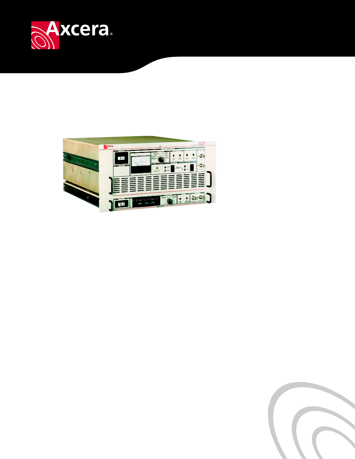
Axcera 117B Compiled User Manual

INSTRUCTION MANUAL
117B
20 WATT VHF HIGH BAND
TRANSLATOR
AXCERA, LLC
103 FREEDOM DRIVE P.O. BOX 525 LAWRENCE, PA 15055-0525 USA
(724) 873-8100 • FAX (724) 873-8105
www.axcera.com • info@axcera.com

117B 20 Watt VHF High Band Translator Table of Contents
- Page 1 of 1 -
Table of Contents
1. Introduction:
2. System – 117B: .................................................................................... 1175-1000
a. System Description
b. Specifications
c. Installation Procedure
d. System Check Out and Operation Procedure
e. Switch Position and Status for Normal Operation
f. System Alignment Procedure
g. Remote Control Interface Connections
h. Drawings:
1. Block Diagram.......................................................................... 1175-3000
2. Interconnect........................................................................... 1175-8000
3. VHF Low Band Receiver Tray:
a. Circuit Description
b. Detailed Alignment Procedure
c. Drawings:
1. Block Diagram.......................................................................... 1265-3100
2. Interconnect........................................................................... 1265-8100
4. 20 Watt VHF High Band Upconverter/Amplifier Tray:
a. Circuit Description
b. Detailed Alignment Procedure
c. Drawings:
1. Block Diagram.......................................................................... 1174-3100
2. Interconnect........................................................................... 1174-8100
5. Subassemblies:
Refer to the subassembly section for the schematics of the boards and subassemblies that
make up the 117B. A drawing list showing the order in which the drawings appear in the
subassembly section is found at the beginning of that section.
6. Maintenance and Harnesses:
This section contains information on proper operation and maintenance of the 117B.

117B 20 Watt VHF High Band Translator System Description
The 117B is a 20 Watt High Band VHF Television Translator which operates at a nominal Internally
Diplexed output power of 20 Watts Peak Sync Visual with typically 2 Watts Aural at a -10 dB
Aural/Visual Ratio.
Functionally, it is comprised of a VHF Low Band Receiver Tray (1265-1100) and a 20 Watt VHF
High Band Upconverter/Amplifier Tray {1355-1010 (Low Band), 1355-1011 (Mid Band) or 1355-1012
(High Band)}.
The Receiver Tray receives the Low Band VHF Channel Input at Jack (J1) and converts it to an
Internally Diplexed Visual + Aural IF Output (+0 dBm) at J4. The Visual + Aural IF output of the
Receiver Tray at J4 is fed to J2 the IF Input Jack for the 20 Watt VHF High Band
Upconverter/Amplifier Tray. The Upconverter Section of the Tray mixes the IF with an internally
generated L.O. to produce the VHF High Band Channel Frequency Output. The signal is amplified
and filtered in the Amplifier Section and directed to J4 the RF Output of the Tray. This output
connects to the Antenna for your System.
Jack J7 located on the back of the Upconverter/Amplifier Tray is a 37 Position "D" Remote Interface
Connector which provides the Operator with a connection for Remote Monitoring and Operation of
the Translator.
This manual provides the Technical Specifications of the Translator, along with the Circuit
Description, Alignment Procedure and the Schematics, Block Diagrams, Interconnects and
Replacement Parts Lists necessary for the proper operation and maintenance of the 117B.
VHF Solid State Transmitter / Translator
110A / 110B / 112B / 113B / 114B /
115A / 115B / 117B / 118B / 119B
■Completely Solid State
■Designed for unattended operation with
built-in remote control interface
■Small size – ideal where space is limited
■Class A amplification up to 20W for
excellent linearity
■Extensive front panel status and metering
■Slide out tray assemblies for ease of
maintenance with no extenders
■BTSC Stereo Ready

VHF Solid State Transmitter / Translator
Visual Performance
Power Output (Peak) 10 / 20 / 50 watts
Output Impedance 50 ohms
Output Connector Type “N”
Frequency Range (low band) 54 to 88 MHz
Frequency Range (high band) 174 to 216 MHz
Carrier Stability (Transmitters
or Translators with FCR) ±250 Hz
Frequency Translation Stability
(Translators) ±250 Hz
Regulation of RF Output Power 3%
Output Variation (over 1 frame) 2%
Sideband Response
-1.25 MHz and below -20 dB
-0.75 to -0.5 MHz +0.5, -2.0 dB
-0.5 to +3.58 MHz ±0.5 dB
3.58 MHz to 4.18 MHz +0.5, -1.0 dB
Freq Response vs. Brightness ±0.5 dB
Visual Modulation Capability 1%
(Transmitters)
Differential Gain 5%
Incidental Phase Modulation ±3°
Linearity (Low Frequency) 5%
Differential Phase ±3°
Signal-to-Noise Ratio 55 dB
2t K-Factor 2%
Envelope Delay
Transmitters Per FCC Standard
Translators ±40 ns
Video Input (Transmitters) 75 ohms
Harmonic Radiation -60 dB
Intermodulation Products -52 dB (red field)
Spurious -50 dB
(>3 MHz from channel edge)
Noise Figure w/input Preamp 6 dB (max.)
(Translators)
Input Dynamic Range -76 to -25 dBm
(Translators)
Aural Performance
Power Output (Average) 1 / 2 / 5 watts
Distortion 0.5%
FM Noise -60 dB
AM Noise -53 dB
Aural to Visual Separation 4.5 MHz, ±100 Hz
(Transmitters)
Composite Audio Input (Transmitters)
Input Level 1V peak, nominal
Input Impedance 75 ohms, unbalanced
Freq (±0.5 dB response) 30 Hz to 120 kHz
Monaural Audio Input (Transmitters)
Input Level 0 to +10 dBm
Input Impedence 600 ohms, balanced
Freq Range (±0.5 dB resp) 30 Hz to 15 kHz
Pre-emphasis 75µs
Subcarrier Input (Transmitters)
Input Level 1V peak, nominal
Input Impedance 75 ohms, unbalanced
Freq Range (±0.5 dB resp) 20 kHz to 120 kHz
General
Operational Temperature Range -30°C to +50°C
Operational Humidity Range 0% to 95%
Altitude up to 8,500 feet
Size (H x W x D)
110A / 115A 7” x 19” x 21”
Transmitters 8.75” x 19” x 21”
(exc 110A / 115A)
Translators 10.5” x 19” x 21”
Weight 30 lbs.
Line Voltage 115/230VAC, ±10%,
1 phase, 50/60 Hz
Power Consumption 250 / 350 / 350 watts
B0001 1101R1-E

117B 20 Watt VHF High Band Translator Installation Procedure
- Page 1 of 2 -
UNPACKING
Please inspect all material thoroughly upon arrival. Axcera certifies that upon leaving our facility
the equipment was undamaged and in proper working order. The shipping container should be
inspected for obvious damage that is indicative of rough handling.
Remove the Cabinet Assembly or if shipped separately, the Receiver Tray, the VHF
Upconverter/Amplifier Tray, the Wire Harness and the Installation Material Kit from the shipping
containers and inspect for damage. Check for dents, scratches or a broken switch, meter or
connector. Remove the top covers from the Trays and again inspect for shipping damage. Extract
all packing material from inside and around the Trays. Check for loose hardware and connectors,
retighten if needed. Any claims against in-transit damage should be directed to the Carrier.
SITE CONSIDERATIONS
There are special considerations which must be made before installing the 117B and this section
will help you plan ahead.
The AC line requirements is an important consideration in Site planning. Each Translator requires a
10 Amp feed.
Another important Site consideration is temperature control. The 117B is rated for operation in an
ambient temperature range of 0° to 45° C. Over temperature problems are far more likely than
under temperature. Over temperature can cause heat related problems such as thermal runaway
or component failure. The Tray contains a Thermal Interlock Circuit that will shut down the
Translator until the temperature drops to an acceptable range.
The Translator requires a cooling system that is adequate for the heat created by the power
dissipation of the Translator. This problem may not surface for many months if the installation is
completed during cool weather, but may suddenly appear during the heat of summer days.
In many cases, a simple heat exhaust system is adequate. A thermostatically controlled fan to
exhaust the heat to the outside works very well if a few guidelines are followed:
1. Check that the fan is large enough. At least 200 CFM per Translator.
2. Place the fan high enough on the wall or in the ceiling where the heat is located.
3. Provide an air intake for cool air. This intake should be on the other side of the room and
low on the wall to allow air to flow over the Translator Cabinet. The intake should also be
large enough to accommodate the capacity of the exhaust fan.
In very hot climates, air conditioning may be required, and cooling capacity must be considered.
The size of the Transmitter Room and the number of Transmitters and/or Translators and other
equipment will determine what size system is required. An HVAC Technician should be consulted.
With both exhaust and air conditioning systems it is better to over estimate the operating capacity
than to under estimate. This provides for a safe operating margin.
Though it is less likely to cause problems, extreme cold should also be anticipated. Extremely low
temperatures may cause condensation inside the Tray due to a large differential between ambient
and internal temperatures. The equipment itself may provide enough heat for normal operation, if
the room is small enough and properly weatherproofed. However, it is better to install a small
heater than to take a chance. The heater will also provide warmth for Technical Personnel if
maintenance or repairs are necessary during the winter months.
INSTALLATION PROCEDURE - CONTINUED
INSTALLATION OF THE TRANSLATOR

117B 20 Watt VHF High Band Translator Installation Procedure
- Page 2 of 2 -
For units that are supplied with a cabinet, remove the Cabinet from the shipping container.
Remove the plastic covering. If the Trays are shipped separately, the shipping material must be
removed from the inside of the Cabinet before the Trays are inserted into the Cabinet. Cut the
cable ties or cord which hold the Tray Harness breakouts to the Tray Slides. Carefully remove the
foam packing material from around the cables, connectors and slides. Do not use a Knife or other
sharp object as these may cut the wires. Slide the Trays into the cabinet, if they are not already
mounted. Check that the cable breakouts for the Trays are not caught in the Trays as they are
slid into place.
If the Trays are shipped mounted in the Cabinet, remove the two metal brackets which hold the
Trays in place during shipment. These are held in place by two screws and must be removed to
allow the Trays to be pulled out for Test.
If the Trays do not slide in and out of the cabinet smoothly, loosen the hardware holding the slides
onto the front of the cabinet and move the Tray up or down to stop it from rubbing. Retighten
after the necessary adjustments have been made.
Secure the small cable retractors, tied to the main harness, to the rear of each Tray by sliding
them into the clip located there. Refer to the rear view of the Trays for more details. Connect
the plugs of the main harness to the corresponding Jack numbers on each Tray, starting with (A2)
the Upconverter/Amplifier Tray. (A1) is the Receiver Tray. (An Example of the numbering is: 1 2
on the cable from the main harness stands for the Receiver Tray A1, AC Input Jack J2).
After the Trays have been installed and all harness connections have been made, connect the
Main AC to the AC Input Box located at the upper, right rear of the Cabinet. 240 VAC, 30 Amp,
#10 AWG, 4 wire is recommended. A Qualified Electrician should do the Main AC Installation. The
AC Input Plug for each Tray should be connected to the AC Outlet Box.
INSTALLATION OF A TRANSLATOR NOT SUPPLIED WITH A CABINET
Two Tray slides are provided for the 1 3/4" Receiver Tray and the 7" VHF Upconverter/Amplifier
Tray. The Receiver Tray should be mounted under the Upconverter/Amplifier Tray. Locate the
Tray slides and install the left slide into the cabinet first. The left side slide is plain with no cable
retractor attached. Mount this slide onto the left side of the cabinet, looking from the rear using
the bolts and nuts provided. Refer to the "Cabinet Mounting Instructions For Tray Slides" drawing
for more details. Check that the slide is level from front to back. NOTE: Allow a spacing of
approximately 5 inches between the end of the stationary section of the slide and the rear
mounting bar of the cabinet to permit normal operation of the cable retractors.
Install the slides onto the right side of the cabinet, looking from the rear. These slides connect
the end bracket, attached to the main harness, to the stationary section of the slide with two #10
hex nuts provided. Now secure the slide by connecting it to the front and rear mounting bars
using #10 bolts and the bar nuts provided.
Connect the plugs from the main harness to the corresponding Jack numbers on each Tray.
(Example: 2 1 means the VHF Upconverter/Amplifier Tray A2, Jack J1). Check that the AC Input
Plugs to the Trays are connected to the AC Outlet Box.
After Installation of the Trays, refer to the Check Out and Operation Procedure for the initial
operation of the Translator.

117B 20 Watt VHF High Band Translator System Check Out and
Operation Procedure
- Page 1 of 1 -
SYSTEM CHECK OUT AND OPERATION PROCEDURE
Connect the output at the "N" Type connector J4 of the 20 Watt VHF Upconverter/Amplifier Tray
to a suitable load or the Antenna for your System. Connect the Low Band VHF Channel RF Input
Signal to Jack J1 located on the rear panel of the Receiver Tray.
Switch the AC Main Circuit Breaker on. Switch On the On/Off Power Switches located on the
Receiver Tray and the VHF Upconverter/Amplifier Tray and observe that the switches light,
indicating AC is present to that Tray. Flip the Operate/Standby Mode Switch located on the VHF
Upconverter/Amplifier Tray and confirm that the LED indicators will also switch. Switch the
Translator to Standby.
The Translator Control (Automatic/Manual) Switch S3, located on the front panel of the VHF
Upconverter/Amplifier Tray, switches the Translator between the Automatic and Manual mode of
operation. In Automatic, the Translator will revert to Standby if the input RF signal is lost. During
Testing of the Translator, Switch S3 to Manual, this will keep the Translator from going to Standby
if the Input RF is removed. Normal Operation is with the switch in the Manual Mode.
Slide the Upconverter/Amplifier Tray out and remove the top cover. Check that switches S1 (ALC)
and S2 (AGC), located on (A10) the ALC/AGC Board (1067-1116) are both in the Automatic
position. Confirm that S1 on (A11) the Linearity Corrector Board (1161-1116) is Enabled. Switch
the Translator to Operate. The Amplifier Status LED (DS4) will light indicating normal current draw
by (A17-A2) the High Band VHF Amplifier Board (1174-1101). The Green Thermal Interlock LED
(DS3) will light indicating that the temperature within the Tray is Normal. Switch the Front Panel
Meter Selector Switch to the Power Supply Voltage position and confirm a reading of +24 VDC, the
voltage produced by (A3) the Switching Power Supply Assembly.
Turn the Front Panel Meter Selector Switch to the % Visual Power Position and verify a reading,
normally 100%, which is the same value as written on the Test Data Sheet for the Translator.
Turn the Meter Selector Switch to the % Aural Power Position and verify a reading which is the
same value as written on the Test Data Sheet for the Translator. The Aural/Visual Ratio is
typically set to 10 dB at the factory. Turn the switch to the % Reflected Power Position and
verify the Test Data Sheet Reflected Power value, <10%. The ALC Reference Voltage Position
should read 2 Volts. The AGC Detector Voltage Position should read .3 Volts.
If the Translator has completed the above System Check Out Procedure, replace the lids of the
Trays and slide them back into place. If a problem occurred in a Tray, refer to the Detailed
Alignment Procedure in that Tray Section of the Manual for more information.
Check that the RF Input Signal is connected to the Receiver Tray. Check that the RF output of
the 20 Watt VHF High Band Upconverter/Amplifier Tray is connected to the antenna for your
System. Check that the Automatic/Manual Switch located on the front panel of the
Upconverter/Amplifier Tray is switched to the Manual position.
You are now ready for the normal operation of the Translator. Set-up of the linearity correctors
are described in the System Alignment Procedure which follows.

117B 20 Watt VHF High Band Translator Switch Position and Status
for Normal Operation
- Page 1 of 1 -
Switch Position and Status for Normal Operation
VHF Low Band Receiver Tray
(A12) IF ALC Board (1109-1402) S1 switched to ALC position.
20 WATT VHF High Band Upconverter/Amplifier Tray
(A10) ALC/AGC Board (1067-1116) S1 switched to ALC position
S2 switched to AGC position
DS2 not lit (Video is Present)
DS3 not lit (No ALC Fault)
DS4 not lit (No AGC Fault)
DS5 not lit (No RF Mute)
(A11) Linearity Corrector Board (1161-1116) S1 switched to Correction in, Enable
(A7) Transmitter Control Board (1161-1109) S1 switched to Modulator, DS5 lit.
DS1 not lit (RF Input is present to the
Receiver Tray). May be lit all the time if
Receiver Tray not used.
DS2 not lit (Video Input to
Upconverter/Amplifier Tray is present).
DS3 not lit (Video Input is present to the
Modulator Tray. May be lit constantly if
Optional Modulator Tray not present.
Front Panel Auto/Manual Switch (S3) Manual position
Front Panel Meter Selector Switch (S1) Selects metering: % Visual Output Power, %
Aural Output Power, % Reflected Power,
Power Supply Voltage, ALC Reference Voltage
and AGC Detector Voltage.

117B 20 Watt VHF High Band Translator System Alignment Procedure
- Page 1 of 2 -
The Translator has been factory aligned and should not require adjustment to obtain normal
operation. For a Detailed Alignment Procedure of each Tray, refer to the Receiver Tray or the 20
Watt Upconverter/Amplifier Tray section of this Manual.
SYSTEM SET UP
The system set-up includes adjustment of linearity to compensate for any amplifiers nonlinear
responses. The Translator should be switched On initially into a 20 Watt dummy load to verify that
the system is functioning properly.
In the VHF Upconverter/Amplifier Tray, check that the ALC Auto/Manual Switch (S1), located on
(A10) the ALC/AGC Board (1067-1116), is in Auto. Switch the On/Off Circuit Breakers located on
the front panels of the Receiver and the 20 Watt Upconverter/Amplifier to the On position. Switch
the Translator to Operate and adjust the ALC Reference Pot (R47), or (R2) the Front Panel Power
Adjust, to obtain a Detected IF Output Voltage Level of +2.0 VDC at TP3 of the ALC/AGC Board.
The Front Panel Meter in the ALC Reference Voltage position should also read +2.0 VDC. Switch
the ALC Auto/Manual Switch (S1) to Manual ALC and adjust the Manual ALC Pot (R17) to obtain a
Detected IF Output Voltage Level of +2.0 VDC at TP3 of the ALC/AGC Board. Switch the ALC
Auto/Manual Switch (S1) to Auto ALC.
In the VHF Upconverter/Amplifier Tray, check that the AGC Switch (S2), located on (A10) the
ALC/AGC Board (1067-1116) is in Auto. Preset the AGC Auto Gain Pot (R96) and the AGC Manual
Gain Pot (R101) to minimum (CCW). Switch the Front Panel Automatic/Manual Switch to Manual.
Switch the front panel Metering Switch, located on the 20 Watt Upconverter/Amplifier Tray, to the
% Visual Output Power position and adjust the AGC Auto Gain pot (R96) located on (A10) the
ALC/AGC Board (1067-1116) to 100% on the meter. Switch the AGC Switch (S2) to the Manual
Position and adjust the AGC Manual Gain pot (R101), located on the ALC/AGC Board, also for 100%
on the meter. Switch S2 back to Automatic. The Front Panel Meter of the Upconverter/Amplifier
Tray in the AGC Detector Voltage position should read +.3 VDC, but the exact values are written
on the Final Test Data Sheet for your System.
Connect a Demodulator and Oscilloscope or other monitoring equipment to monitor the differential
gain and differential phase of the output signal. If a synchronous demodulator having a quadrature
video output is available, it may be employed with an X-Y Oscilloscope to display incidental carrier
phase modulation (ICPM). As shipped, the Translator was preset to include linearity (gain vs.
level) predistortion which was adjusted to compensate for the corresponding non-linear distortions
of the solid state amplifier devices in the Translator. Switch S1 located on (A11) the Linearity
Corrector Board (1161-1116), to the On position.
SYSTEM SET UP OF LINEARITY
The IF linearity correction function consists of three non-linear cascaded stages, each having an
adjustable magnitude and a threshold, cut-in point. The threshold adjustment determines at what
IF signal level the corresponding corrector stage begins to increase gain. The magnitude
adjustment determines the amount of gain change for the part of the signal which exceeds the
corresponding threshold point. Because the stages are cascaded, the order of correction is
important.
The first stage should cut-in nearest the white level, with the cut-in point of the second stage
moving toward black, with the last stage primarily stretching sync. Linearity Corrector Board pots
R3, R13 and R23 control the overall gain of each stage. They were preset during Final Test at the
Factory and should not require adjustment. If moved accidentally, typical settings are R3, R13 and
R23 mid-range.
SYSTEM SET UP OF LINEARITY - CONTINUED

117B 20 Watt VHF High Band Translator System Alignment Procedure
- Page 2 of 2 -
To adjust the linearity correction from scratch, preset the Linearity Corrector pots R5, R16 and R26
(threshold) to CCW and Linearity Corrector pots R2, R11 and R22 (magnitudes) CW. Insert a 3.58
MHz modulated staircase or ramp video test signal into the Tray and monitor the differential gain of
the output. Switch the ALC Auto/Manual Switch (S1) located on (A10) the ALC/AGC Board to
Auto ALC. This completes the ALC loop.
Adjust the ALC Reference Pot (R47), or the Front Panel Power Adjust, to obtain a Detected IF
Output Voltage Level of +2.0 VDC at TP3 of the ALC/AGC Board. The Front Panel Meter in the ALC
Reference Voltage position should also read +2.0 VDC. Switch the ALC Auto/Manual Switch (S1)
located on (A10) the ALC/AGC Board to Manual ALC and adjust the Manual ALC Pot (R17) to obtain
a Detected IF Output Voltage Level of +2.0 VDC at TP3 of the ALC/AGC Board. Switch the ALC
Auto/Manual Switch (S1) located on (A10) the ALC/AGC Board to Auto ALC. The ALC will now
operate to maintain the corresponding peak power level following the correctors. Therefore, the
linearity adjustment procedure should be repeated to achieve the correct differential gain
predistortion. A positive aspect of linearity adjustment with ALC and AGC enabled is that the
control movements will not affect peak power. This completes the preset steps.
While observing Differential Gain, adjust the first linearity stage and advance the Threshold #1
Control (R5) CW to stretch the signal above the White and Mid-Luminance region. Back off on the
corresponding Magnitude #1 Control (R2) as required. Next, advance the Threshold #2 Control
(R16) to stretch the Black and Sync levels, then back off on the Magnitude #2 Control (R11) as
required. Adjust the Threshold #3 Control (R26) to further stretch the Black and Sync levels.
Back off on the corresponding Magnitude #3 Control (R22) as required. Go back through the White
through Black and Sync correctors to touch up the effects of ALC Level changes during the
adjustment. If the amplifier is being driven very close to saturation, it may not be possible to get
enough Sync Stretch while maintaining a flat differential gain. The IF linearity correctors, when
properly adjusted, will provide excellent lower sideband suppression and minimum frequency
response change vs. level. These results are achieved by generating intermod products which
cancel with those produced by the amplifier, an effect which is not possible with video correction.
FINAL AGC ADJUSTMENT
Check that the ALC Voltage is set to +2.0 VDC at TP3. Switch the front panel Metering Switch,
located on the Front Panel of the VHF Upconverter/Amplifier Tray, to the % Visual Output Power
position and adjust the AGC Auto Gain pot (R96) located on the ALC/AGC Board to 100% on the
meter. Switch the AGC Switch (S2) the Manual Position and adjust the AGC Manual Gain pot
(R101), located on the ALC/AGC Board, also for 100% on the meter. Switch S2 back to Automatic.
The Front Panel Meter of the Upconverter/Amplifier Tray in the AGC Detector Voltage position
should read (.3 VDC) and in the ALC Reference Voltage Position (2 VDC), but the exact values are
written on the Final Test Data Sheet for your System.
This completes the System Alignment Procedure for the 117B.

117B 20 Watt VHF High Band Translator Remote Control Connections
- Page 1 of 1 -
Remote Control Interface Jack (J7) 37 Position "D" Connector
Function Connector Interface Type
Rmt Operate Command J7 Pin 1 Contact Closure
Rmt Operate/Standby Rtn J7 Pin 2
Rmt Standby Command J7 Pin 3 Contact Closure
Rmt Operate Indicator J7 Pin 4 50mA Max. Current Sink
Rmt Operate Indicator Rtn J7 Pin 5
Rmt Standby Indicator J7 Pin 6 50mA Max. Current Sink
Rmt Standby Indicator Rtn J7 Pin 7
Rmt Aural Power Metering J7 Pin 8 1v Full Scale At 1k
Rmt Aural Pwr Metering Rtn J7 Pin 9 Source Resistance
Rmt Reflected Power Mtring J7 Pin 10 1v Full Scale At 1k
Rmt Reflected Pwr Mtr Rtn J7 Pin 11 Source Resistance
Rmt Visual Power Mtring J7 Pin 12 1v Full Scale At 1k
Rmt Visual Power Mtring Rtn J7 Pin 13 Source Resistance
Rmt Visual + Aural Pwr Mtr J7 Pin 14 1v Full Scale At 1k
Rmt Vis + Aural Pwr Mtr Rtn J7 Pin 15 Source Resistance
Rmt Am I.D. Indicator J7 Pin 20 50ma Max. Current Sink
Rmt Am I.D. Indicator Rtn J7 Pin 21
Notes: These functions are accessed through the 37 position "D" connector (J7) located on the
rear panel of the VHF High Band Upconverter/Amplifier Tray.
J7 Pins 16 - 19 are not used in this Translator.

117B 20 Watt VHF High Band Translator UHF/VHF Receiver Tray,
w/(Opt) Frequency Correction
Circuit Description
- Page 1 of 3 -
The UHF/VHF Receiver Tray w/(Optional) Frequency Correction selects the desired UHF or VHF On
Channel Input Signal and converts it to a Combined IF Signal of 45.75 MHz Visual + 41.25 MHz
Aural. The Tray also has provisions for a Frequency Correction Option that consists of a VCXO
Channel Oscillator Assembly with a PLL Circuit which maintains an exact IF Output Frequency, over
the capture range of the PLL circuit, even if the Input UHF or VHF Frequency may vary.
RF Input Signal Path
The RF Input to the Tray, (-61 dBm to -16 dBm in Level), is fed through J1 for 50Ω to (A7) the
input 50Ω Filter, DC Multiplexed (1035-1204 UHF, 1035-1902 VHF LB or 2065-1024 VHF HB) or
through J5 for 75Ω to (A7) the 75Ω input Filter, DC Multiplexed (1035-1207 UHF, 1035-1903 VHF
LB or 2065-1023 VHF HB), which is of a double tuned design that is adjusted to the desired Input
UHF or VHF Channel Frequency. Note: If the input signal is greater then -25dBm, an attenuator
should be used to limit the level to -25dBm. +12 VDC, for use by an (Optional) external
Preamplifier Assembly, connects to the filter through F1 a 1 Amp Fuse. This +12 VDC is DC
Multiplexed onto the input signal cable from the Preamplifier. DS1 a Red LED located on TB1 in the
Tray will be lit if the +12 VDC is present on the input cable. If a Preamplifier is not used, F1 should
be removed and DS1 should not be lit.
The signal is next amplified +12 dB to approximately the -49 to -4 dBm level by a low noise
amplifier located on (A8-A1) the Dual Stage Amplifier Board (1227-1501) that is contained in (A8)
the Dual Stage Amplifier Assembly (1227-1503). The board has approximately +13 dB or +26 dB of
gain, depending on whether Jumper W1 on J5 is in place. The signal is then filtered in (A9) a
Channel Filter (1007-1101 UHF, 1034-1202 VHF LB or 2065-1000 VHF HB) and then applied back to
(A8-A1) the Dual Stage Board where the same amplification takes place. Jumper W1 on J7,
located on the Dual Stage Board, should be removed if the Receiver Input level is greater than -
40dBm. The output is connected to (A10) the Downconverter Amplifier Assembly (1227-1505) that
contains (A10-A1) the Downconverter Amplifier Board (1227-1502). The RF, at the -47 dBm to -2
dBm Level, connects to the "R" Input Jack of the Mixer Z1 located on the Downconverter Amplifier
Board.
Local Oscillator Signal Path
The Local Oscillator Signal is derived from a cut to channel crystal mounted in an oven that is
factory set at 45° C. The Oscillator operates at 1/8 for UHF, 1/4 for VHF High Band or 1/2 for VHF
Low Band of the desired local oscillator frequency. The crystal is mounted on (A4-A1) the Channel
Oscillator Board, Dual Oven (1145-1201), that is part of the Channel Oscillator Assembly (1145-
1202). The oscillator circuitry is a modified Colpitts design operating in a separate oven set at 50°
C. for improved stability. If the Frequency Correction Option is purchased, the VCXO Channel
Oscillator Assembly (1145-1206), which contains the VCXO Channel Oscillator Board (1145-1204),
is used in place of the standard Channel Oscillator Assembly, and an AFC voltage from the PLL
circuit maintains the frequency of the VCXO.
The output of the Channel Oscillator is connected to the (A5-A1) the x8 Multiplier Board
(1227-1002) for UHF, the x4 Multiplier Board (1227-1525) for VHF HB or the x2 Multiplier Board
(1227-1524) for VHF LB, which is located in (A5) the Multiplier Enclosure (1265-1125). The proper
multiplier board takes the output of the Channel Oscillator (+3 dBm) and multiplies it eight, four or
two times by a series of three, two or one x2 Broadband Doublers (2x2x2 = x8), which produces
the L.O. signal on the desired frequency needed for the upconversion process. The signal is then
amplified to the +16 dBm level. A sample of the multiplied L.O. Signal is fed to a detector circuit
which lights the Green LED DS1 that indicates that the L.O. is present at the Output Jack J2 of the
Multiplier Board. This Green LED is seen through a hole the lid of the Multiplier Assembly and is an
indication, when lit, that there is a signal present at the output of the Multiplier Board. The L.O.
signal is filtered in (A6) a L.O. Filter 1007-1101 UHF, 2065-1000 VHF HB or 1034-1211 VHF LB) and
then sent (+15 dBm) to J2 on (A10-A1) the Downconverter Amplifier Board. The L.O. Input to the
Downconverter Amplifier Board is connected thru a 3 dB matching pad to the "L" Input of the Mixer
(Z1) at a +12 dBm level.

117B 20 Watt VHF High Band Translator UHF/VHF Receiver Tray,
w/(Opt) Frequency Correction
Circuit Description
- Page 2 of 3 -
Combined IF Signal Path
The L.O. and the RF signals are mixed in the Mixer Stage of the Downconverter Amplifier Board to
produce the desired IF difference frequency at -55 dBm to -10 dBm in level, depending on the RF
Input Level. The Combined IF Signal is routed to (A11-A1) the IF Filter/ALC Board (1227-1504),
which is mounted in (A11) the IF Filter/ALC Enclosure (1265-1105). The IF Filter/ALC Board
contains a Pin Diode Attenuator circuit which is part of the Automatic Level Control (ALC) that
controls the level of the IF Signal to the two stage amplifier ICs U1 and U2.
The (Optional) (A11-A2) SAW Filter/Amplifier Board (1035-1211) is also contained in the IF
Filter/ALC Enclosure. The SAW Filter/Amplifier Board connects to J5 and J6 of the IF Filter/ALC
Board if more attenuation of the Out Of Band products is needed. If the SAW Filter/Amplifier Board
is not needed, a jumper connects the Combined IF from J5 to J6 on the IF Filter/ALC Board.
The Combined IF is then bandpass filtered to the needed 6 MHz IF bandwidth around the 41.25
MHz + 45.75 MHz Combined IF signal and amplified by U3 to the -41 dBm to +4 dBm Level before it
is split. One output is detected by U4 for use as the ALC reference level to the Pin Diode
Attenuator Circuit. The ALC comparator drives the Pin Diode Attenuator Circuit to maintain the
desired output level, typically +2 dBm. The other split output connects to J2 the Combined IF
Output of the board that is cabled to the IF Output Jack of the Tray at J4 (+2 dBm).
Frequency Correction Option
If the Frequency Correction Option (1227-1528) is purchased, (A13) the IF Filter/Limiter Board
(1109-1001), (A14) the IF PLL Board (1109-1002), the (A15) IF Carrier Oven Oscillator Board
(1100-1206), (A4) the VCXO Channel Oscillator Assembly (1145-1206) and (A16) an IF Amplifier
Board, High Gain (1197-1126) are part of the System.
A Sample of the amplified and ALC controlled signal from the IF Filter/ALC Board is directed to the
IF Amplifier Board, High Gain (1197-1126) where it is amplified and connected to J2 on (A13) the IF
Filter/Limiter Board (1109-1001). The IF is filtered by a SAW Filter, which passes Visual Carrier and
Aural Carrier only, and amplified before it is split. The Aural IF Output is not used in this Tray. The
other output of the splitter is amplified and applied to a Notch Filter. The Notch Filter is tuned to
the Aural Frequency by C17 and R10 which reduces or eliminates the Aural IF from the Visual IF
signal. The Visual IF Only signal then connects to a video detector circuit which in conjunction
with U5 strips the video from the Visual IF signal. The IF CW Signal is amplified and buffered
before it is connected to the output of the board at J6. The IF CW connects to J2 of (A14) the IF
PLL Board (1109-1002).
The IF CW Signal (+3 dBm) on the IF PLL Board is wired to U1 a Divider IC which, in conjunction
with U2, sets up one of the reference signals to the comparator circuit. The other reference signal
is derived from the 50 kHz reference Input at J4 which is a divided down 50 kHz sample of the 38.9
MHz signal generated on (A15) the IF Carrier Oven Oscillator Board (1100-1206). The 38.9 MHz IF
Carrier Oven Oscillator Board is used instead of the 45.75 MHz IF Carrier Oven Oscillator Board to
minimize the interference between the generated 45.75 MHz IF and the signal generated on the
(A15) IF Carrier Oscillator Board. The 38.9 MHz signal itself is not used, just the divided down 50
kHz reference of the 38.9 MHz Signal is used. The two reference signals applied to the IF PLL
Board are compared by U2 and a difference voltage (AFC) is produced. The difference voltage
(AFC), approximately -3 VDC, is fed from J3 of the board to FL2 of (A4) the VCXO Assembly. If
the frequency of the VHF or UHF Input to the Tray should drift, the ALC voltage will change to
increase or decrease the output frequency of the VCXO Assembly which increases or decreases
the L.O. Frequency that maintains the IF Frequency at the standard 45.75 + 41.25 MHz
Frequency. If the frequency of the Input Signal should drift out of the capture range of the PLL
Circuit, DS1 the Red LED Unlock Indicator, located on the IF PLL Board, lights.
Voltages for Operation of the Tray

117B 20 Watt VHF High Band Translator UHF/VHF Receiver Tray,
w/(Opt) Frequency Correction
Circuit Description
- Page 3 of 3 - January 7, 2002
The AC input to the Tray is 117 VAC or 230 VAC and is directed thru Jack J2, of the (A1) Power
Entry Module (1265-1104), to the step down Toroid (A2). The Power Entry Module contains an
On/Off Switch, a 4 Amp Slo-Blo Fuse and three MOVs which protect the Tray from transients or
surges which may occur on the AC Input Lines. When the On/Off Switch is switched On, AC is
applied to the (A2) Toroid. The Toroid steps down the voltage into two 16 VAC outputs which are
fed to (A3) the +12V(3A)/-12V Power Supply Board (1092-1206). The 16 VAC Inputs are
connected to the two full wave bridge networks one for +12 VDC and one for -12 VDC. The
output of the +12 VDC rectifier is fed to three 7812 IC regulators (U1, U2 and U3) and the output
of the -12 VDC rectifier is fed to one 7912 IC regulator (U4). The ±12V Power Supply Board
provides the voltage regulated and current limited +12 VDC and -12 VDC to the rest of the boards
in the Tray.
+12VDC for External Preamplifier
+12 VDC is also applied through a 1 Amp Fuse F1 to (A7) the input DC Multiplexed UHF or VHF
Filter. The +12 VDC is multiplexed in the Filter onto the input coaxial cable that connects from the
(Optional) Remote Preamplifier Unit to the Receiver Tray. This supplies the Preamplifier with the
+12 VDC needed for operation. The Red LED DS1 mounted on the Terminal Block TB1 will be lit if
the +12 VDC is applied to the coaxial cable. Note: If the Red LED, DS1, is lit, the +12 VDC may
damage Test Equipment that is connected to the input of the Receiver Tray. If a Preamplifier
Assembly is not part of your System, F1 should be removed, therefore DS1 should not be lit and
the +12 VDC is not multiplexed onto the input coaxial cable. A spare Fuse for F1 is supplied and
stored near the fuse holder for F1.

117B 20 Watt VHF High Band Translator UHF/VHF Receiver Tray,
w/(Optional) Frequency Correction
Detailed Alignment Procedure
- Page 1 of 4 -
Connect a UHF or VHF Input with a Multiburst Test signal applied, that is at the desired Channel
Frequency, to J1 50Ω or J5 75Ω located on the rear of the (A3) VHF/UHF Receiver Tray. Check
that the On/Off Switch located on the rear of the Tray is On.
Note: If the Red LED, DS1 is lit, +12 VDC is present at the input of the Receiver Tray and may
damage any test equipment connected to it. Remove the fuse F1, DS1 will not be lit, before
connecting test equipment to the input jack of the Receiver Tray.
(A7) UHF Filter, DC Multiplexed (1035-1204, 50Ω or 1035-1207, 75Ω), VHF Filter, LB, DC
Multiplexed (1035-1902, 50Ω or 1035-1903, 75Ω) or VHF Filter, HB, DC Multiplexed (2065-1024,
50Ω or 2065-1023, 75Ω)
The input UHF or VHF signal (-61 dBm to -16 dBm) is fed to the filter which has been factory
swept for 6 MHz Bandwidth at the Channel frequency and should not be tuned in the field. The
output of the filter is directed to the J1 input of (A8) the Dual Stage Amplifier Assembly.
(A8-A1) Dual Stage Amplifier Board (1227-1501)
Mounted in: (A8) a Dual Stage Amplifier Assembly (1227-1503).
The Dual Stage Amplifier Board has been factory set to the channel frequency and contains no
customer tuning adjustments. The board has approximately +13 dB or +26 dB of gain, depending
on whether Jumper W1 on J5 is in place.
(A9) UHF Filter (1007-1101), VHF LB Filter (1034-1202) or VHF HB Filter (2065-1000)
The UHF or VHF Filter has been factory swept for 6 MHz Bandwidth at the Channel Frequency and
should not be tuned in the field. The output of the filter (-50 dBm to -5 dBm) is fed either through
the additional amplifier stage on the Variable Gain Amplifier Board or to (A10-A1) the
Downconverter/Filter Board.
(A4) Channel Oscillator Assembly, Dual Oven (1145-1202)
Contains: The Channel Oscillator Board, Dual Oven (1145-1201).
1. Connect the main output of the Channel Oscillator (J1) to a spectrum analyzer, adjusted to
view the crystal frequency, and peak the tuning capacitors C6 and C18 for maximum output.
Then tune L2 and L4 for maximum output. The output level should be approximately +5
dBm and the Oven Temperature should be maintained at 50°C.
If a spectrum analyzer is not available, connect a DVM to TP1 on the x8, x4 or x2 Multiplier
Board. Tune capacitors C6 and C18 for maximum voltage at TP1. Then tune L2 and L4 for
maximum voltage at TP1.
2. Connect the sample output of the Channel Oscillator at J2 to a suitable counter and tune
C11, Coarse Adjust, and C9, Fine Adjust, to the crystal frequency. Do not re-peak C6, C18,
L2 or L4 because this may change the output frequency.
Note:While adjusting C9 and C11 to the crystal frequency the peak voltage monitored at TP1 of
the Multiplier Board should not decrease. If a decrease does occur a problem with the
crystal is likely.
3. Reconnect the main output at J1 of the Channel Oscillator to the Input Jack J1 of the
Multiplier Board.

117B 20 Watt VHF High Band Translator UHF/VHF Receiver Tray,
w/(Optional) Frequency Correction
Detailed Alignment Procedure
- Page 2 of 4 -
(A4) Channel Oscillator Assembly, Dual Oven (1145-1202) - Continued
Contains: The (A4-A1) Channel Oscillator Board, Dual Oven (1145-1201).
Note:If the Optional Frequency Correction Kit is purchased a VCXO Assembly (1145-1206),
containing a VCXO Board (1145-1204), will be used instead of the standard Channel
Oscillator Board. The adjustment will be the same as above except that the frequency is
adjusted by moving the Jumper W1 on Jack J6, located on the IF PLL Board (1109-1002), to
Pins 2 & 3, Fixed Bias, and adjusting R15 on the IF PLL Board for -3 VDC at FL2 of the VCXO
Assembly. Move the Jumper W1 on Jack J6 to between Pins 1 & 2, AFC. Connect the
Oscillator Sample output, at (J2) of the Channel Oscillator or the Front Panel Sample Jack
(J9), to a suitable Frequency Counter and tune C11, Coarse Adjust, to the desired
frequency. Do not re-peak C6, C18, L2 or L4 because it may change the output frequency.
Reconnect the main output (J1) of the Channel Oscillator (+5 dBm) to the input (J1) of the
Multiplier Board. DS1 the Red Unlock Indicator, located on the IF PLL Board, should not be
lit.
(A5-A1) x8 Multiplier Board (1227-1002), x4 Multiplier Board (1227-1525) or x2 Multiplier Board
(1227-1524)
Mounted in (A5) a Multiplier Enclosure (1265-1125).
During Normal operation, the Green LED DS1, which can be seen through the access hole in the
Enclosure Assembly, will be lit to indicate that the L.O. is present at the output of the x8 Multiplier
Board.
1. Connect a Spectrum Analyzer to the Output Jack (J2) of the board.
2. Tune C4, C6, C10, C12, C18 and C20 on the x8 and the appropriate caps on the other
boards for maximum output. Readjust all the Capacitors to minimize the seventh and the
ninth harmonics, they should be at least -30 dB down, without affecting the x8 Multiplier
Output.
If a Spectrum Analyzer is not available a DC voltmeter can be used as follows but the harmonic
frequencies must be minimized to prevent interference with other Channels.
1. While Monitoring each Test Point with a DC voltmeter, maximize the voltage by tuning the
Broadband Multipliers in the following sequence.
2. For x8 Multiplier Board: Monitor TP1 with a DVM and tune C4 for maximum. (Typical .6 VDC)
Monitor TP2 and tune C6 and C10 for maximum. (Typical 1.2 VDC)
Monitor TP3 and tune C12 and C18 for maximum. (Typical 2 VDC)
Monitor TP4 and tune C20 for maximum.
Re-peak C12 and C10 while monitoring TP4. (Typical 3.5 VDC)
For x4 Multiplier: Monitor TP1 with a DVM and tune C4 for maximum. (Typical .6 VDC)
Monitor TP2 and tune C6 and C10 for maximum. (Typical 1.2 VDC)
Monitor TP3 and tune C12 for maximum.
Re-peak C12 and C10 while monitoring TP3. (Typical 2 VDC)
For x2 Multiplier: Monitor TP1 with a DVM and tune C4 for maximum. (Typical .6 VDC)
Monitor TP2 and tune C6 for maximum.
Re-peak C4 and C6 while monitoring TP2. (Typical 1.2 VDC)
The Green LED DS1 should be lit which indicates that the L.O. is present at the Output Jack J2 of
the Multiplier Board. The output of the Multiplier at J2 is connected to (A6) a UHF or VHF Filter.

117B 20 Watt VHF High Band Translator UHF/VHF Receiver Tray,
w/(Optional) Frequency Correction
Detailed Alignment Procedure
- Page 3 of 4 -
(A6) UHF Filter (1007-1101), VHF LB Filter (1034-1211) or VHF HB Filter (2065-1000)
This filter has been factory swept at the L.O. frequency and should not be tuned without proper
equipment. The output of the filter (+15 dBm) is connected to J2 on (A10) the
Downconverter/Filter Assembly.
(A10-A1) Downconverter/Amplifier Board (1227-1502)
Mounted in: The (A10) Downconverter/Amplifier Assembly (1227-1505).
The Mixer contains no adjustments and has a L.O. input of approximately +12 dBm in level applied
to J2 and a -47 dBm to -2 dBm RF input applied to J1. The output IF level at J3 will be -55 dBm to
-10 dBm.
1. Connect a Spectrum Analyzer to the Output Jack J3 and adjust L1, C2 and L3 for best
frequency response.
2. Adjust C8 and R3 to notch out the Aural IF Frequency.
The IF output at J3 (-55 dBm to -10 dBm) is fed to the IF Filter/ALC Board. If needed a 10 dB Pad
can be added to the circuit by moving the jumpers on J4 and J5 to the In position.
(A11-A1) IF Filter/ALC Board (1227-1504)
Mounted in: The (A11) IF Filter/ALC Enclosure (1265-1105).
1. Check that Switch S1, located on the IF Filter/ALC Board, is in the Auto ALC and that the
output of the Board at J2 is approximately 0 dBm Output, adjust R23 if needed.
(Optional) (A11-A2) SAW Filter/Amplifier Board (1035-1211)
Mounted in: The (A11) IF Filter/ALC Enclosure (1265-1105).
This board is used for additional adjacent Channel rejection only if needed and may not be part of
the Tray.
The board contains no tuning adjustments. The Jumpers W1 and W2 on J4 and J5 are placed for
Attenuator In or Attenuator Out as needed to give the same output level at J2 as was at J1.
(A2) ±12V Power Supply Board (1092-1206)
This board contains no adjustments.
Note:If the (Optional) Frequency Corrector Kit is part of the tray, perform the following
adjustments. If the Frequency Corrector Kit is not part of the tray, the tray is aligned and
ready for normal operation.
(Optional) (A15) IF Carrier Oscillator Board (1100-1206)
1. Monitor J3 with a Spectrum Analyzer and observe the 38.9 MHz Visual IF signal at +5 dBm.
2. Connect a Frequency Counter to J2 on the board or to J9 on the Front Panel and adjust C17
for 38.9 MHz.

117B 20 Watt VHF High Band Translator UHF/VHF Receiver Tray,
w/(Optional) Frequency Correction
Detailed Alignment Procedure
- Page 4 of 4 -
(Optional) (A15) IF Carrier Oscillator Board (1100-1206) - Continued
3. Connect a Frequency Counter to J1 and check for the 50 kHz signal. Adjust C17, if needed,
to attain the 50 kHz frequency. Remove the Jack on J5. DS2 the Unlock Indicator should
light. Replace the Jack onto J5.
(Optional) (A13) IF Filter/Limiter Board (1109-1001)
1. Monitor the Aural Notch Test Output of the board at J5 and move the Jumper W1 on Jack J4
to between Pins 2 & 3, Test Position. Adjust C17 to the Aural IF Frequency, then adjust
R10 to eliminate or minimize the Aural IF signal. Move the Jumper W1 on Jack J4 back to
between Pins 1 & 2, Operate Position.
2. Monitor the IF CW Output of the board at J6 with an Oscilloscope and adjust R12 and C21
for maximum Video Signal or connect a Spectrum Analyzer, in Zero Span, to J6 and adjust
R12 and C21 for Minimum Video Signal amplitude ripple on the displayed signal.
3. Adjust R15 for +3 dBm or Maximum output level if +3 dBm cannot be attained.
(Optional) (A14) IF PLL Board (1109-1002)
Check that the Red LED DS1, Unlock Indicator, located on the board is not lit.
If DS1 is lit, follow the alignment procedure for setting up the VCXO Channel Oscillator using R9 on
the IF PLL Board to set up the AFC Voltage for the Frequency of the VCXO. If it is still lit, check
the 50 kHz reference output of the (A15) IF Carrier Oven Oscillator. If needed, follow the
alignment procedure for the IF Carrier Oven Oscillator Board.
(Optional) (A16) IF Amplifier Board, High Gain (1197-1126)
This board contains no customer adjustments. The amplified IF output from the IF Filter/ALC Board
connects to the IF Filter Limiter Board.
The Receiver Tray is now set up and ready for normal operation.

117B 20 Watt VHF High Band Translator Upconverter/Amplifier Tray
Circuit Description
- Page 1 of 3 -
The VHF Upconverter/Amplifier Tray takes the modulated Visual + Aural IF input from the Modulator
or Receiver Tray and mixes it with a generated L.O. to produce the desired VHF High Band Channel
Frequency output. The Tray then amplifies the VHF signal to the 20 Watt peak of Sync Visual
Output power level.
IF SIGNAL PATH
The input of the Upconverter/Amplifier Tray is a modulated Internally Diplexed IF signal. The IF
input network for the Tray is a simple bandpass filter located on (A10) the ALC/AGC Board
(1067-1116) which eliminates harmonics on the input signal. The signal is next adjusted in level by
the pin attenuator/ALC circuitry and sent to (A11) the Linearity Corrector Board (1161-1116). The
Linearity Correctors compensate for the amplitude non-linearities of the final amplifiers by providing
an opposite amplitude transfer function. The shape of this transfer function is set by the
potentiometers located on this board. The corrector circuits can also be bypassed by the
switches located on the board.
The output of the Linearity Corrector Board is sent back to the ALC/AGC Board where an AGC
circuit compares a detected sample of the IF with a detected sample of the RF Output and adjusts
the IF output to maintain a constant gain after the first sample point. This corrects for any
temperature drift that may occur in the amplifier devices. (A9) The AGC Control Board (1137-
1201) provides adjustments of the AGC feedback from the Transmitter Control Board to the VSWR
Cutback circuit located on the Transmitter Control Board.
The ALC and AGC controlled IF signal from J4 on the board is fed to Jack (J2) located on (A16) the
Mixer/Amplifier Enclosure, which contains (A16-A1) a Filter/Mixer Board and (A16-A2) a
Filter/Amplifier Board. The IF Signal (-3 dBm Visual -13 dBm Aural) connects to Jack J7 of (A16-
A1) the Filter/Mixer Board (1150-1102) and is wired to the Mixer stage Z1. The Mixer mixes the IF
with the local oscillator signal, that connects to J3 on the board, to produce the desired VHF
output signal.
L.O. SIGNAL PATH
The local oscillator signal is derived from a cut to channel crystal, located in an oven set at 45° C.
This oscillator circuit, which is part of (A14-A1) the Channel Oscillator Board (1145-1201), is a
modified Colpitts circuit. The Channel Oscillator Board is mounted in (A14) a Channel Oscillator
Assembly (1145-1202) that has a separate oven set at 50° C for improved stability. The output of
the Oscillator Assembly at J1 is fed to (A15) a x4 Multiplier Board (1174-1112). The x4 Multiplier
contains two doubler circuits which multiply the L.O. signal to the required frequency needed for
mixing with the IF to produce the VHF High Band Channel Frequency. The L.O. Signal (+5 dBm)
from J2 on the board is connected Jack J1 of (A16) the Mixer/Amplifier Enclosure which is cabled to
Jack (J3) of (A16-A1) the VHF Filter/Mixer Board (1150-1102). The L.O. Signal is amplified by U2
and connected to J4 of the Board. The amplified L.O. Signal at (+14 dBm) is jumpered to (J5) the
L.O. Input Jack to the Mixer Z1.
RF SIGNAL PATH
The L.O. input and the IF input are mixed to produce an output of the Mixer at Jack (J6) (-14 dBm)
which contains the unwanted Mixer products along with the desired VHF Channel signal. These
signals are jumpered from J6 to J1 the RF Input Jack of the VHF Filter/Mixer Board.
RF SIGNAL PATH - CONTINUED

117B 20 Watt VHF High Band Translator Upconverter/Amplifier Tray
Circuit Description
- Page 2 of 3 -
The RF Signal is bandpass filtered for the desired VHF Channel frequency and then amplified by U1
(-2 dBm Visual -12 dBm Aural) before it is connected to the RF Output Jack (J2) of the Board. The
VHF output is connected to J7 of (A16-A2) the VHF Filter/Amplifier Board (1150-1101) on which it
is filtered again and jumpered from J6 to J1 on the board. The +12 VDC needed for operation of
the Filter/Mixer Board and the Filter/Amplifier Board are provided by (A6) the +12V(3A)/-12V Power
Supply Board (1092-1206). The filtered VHF is amplified to +8 dBm and -2 dBm, R9 sets the gain
of the Filter/Amplifier Board using a Pin-Attenuator circuit, and connected to J2 the RF Output of
the Board.
J2 is cabled to J3 on the Mixer/Amplifier Enclosure Assembly. The RF is connected to Jack (J1) on
(A17-A1) the VHF High Band Driver Board (1174-1107). The Driver Board contains a dual transistor
stage Q1 that produces an output of +26 dBm Visual +16 dBm Aural. (A17-A1) The VHF High Band
Driver Board and (A17-A2) the VHF High Band Amplifier Board are mounted on (A17) the Amplifier
Heatsink Assembly (1174-1111). The output of the Driver Board connects to J1 of (A17-A2) the
VHF High Band Amplifier Board (1174-1101). The VHF High Band Amplifier Board contains a dual
Transistor Stage that amplifies the VHF Signal to +44 dBm Visual and +34 dBm Aural. R5 and R9 on
the board are Bias Adjustments which set the gain of the Board. The VHF High Band Driver Board
and the High Band VHF Amplifier Board receive their +26 VDC Bias voltage from (A3) the +26 VDC
Switching Power Supply. DS4 the front panel mounted Amplifier Status LED, that is mounted
across J3-2 and J3-3 of the VHF High Band Amplifier Board, will light if the +26 VDC is present to
the board. The +26 VDC is connected to the board through (F1) the 8 Amp Fuse. The output of
the VHF High Band Amplifier Board at J2 (+44 dBm Visual and +34 dBm Aural) is connected to (A18-
A1) a Low Pass Filter Board (1174-1102, 1174-1103 or 1174-1104 depending on frequency) which
contains a Low Pass Filter and a 2nd Harmonic Trap. The filtered output is cabled to (A18-A2 &
A3) two Trap Filter Boards (1174-1105 or 1174-1106 depending on frequency) each Board contains
two Trap Filter circuits. The first Trap Filter circuit, containing C6 and C8, is tuned to -4.5 MHz
while the second Trap Filter, containing C2 and C4, is tuned to +9 MHz. The output of (A18-A3)
Trap Filter Board connects to Jack (J1) of (A23) a High Band VHF Coupler Board (1141-1002). The
VHF Channel Frequency Output of the Coupler at J2 is directed to the rear of the Tray, the RF
Output Jack (J4), (+43 dBm Visual and +33 dBm Aural).
A Forward Output Power Sample at J3 and a Reflected Output Power Sample at J4 are provided by
the VHF Coupler. The Forward Power Sample is sent to (A24) a Splitter Assembly which provides
two Forward Power Sample outputs that are connected to J1 and J2 on (A26) the Visual/Aural
Metering Board (1161-1103). The Visual + Aural Forward Sample at J1 enters the board which is
tuned to provide an Aural Only Output Sample at Jack J6 - Pin 1 that connects to the front panel
meter for monitoring. The Visual + Aural Forward Power Sample at J2 enters the board which is
tuned to produce a Visual Only Output Sample at Jack J7 - Pin 1 that connects to the front panel
meter for monitoring. The Reflected Sample from J4 of the VHF Coupler connects to J4 of the
Visual/Aural Metering Board and provides a Reflected Output Sample at Jack J9 - Pin 1 that
connects to the front panel meter for monitoring.
SYSTEM CONTROL AND OPERATION
The system control for the Translator consists of (A7) the Transmitter Control Board (1161-1109)
which provides control of the System Operation and the monitoring of the Status of the Tray and
the System. The board provides or removes the commands for operation of the System.
Associated with the Transmitter Control Board are front panel LEDs for monitoring of Operate
(DS5)/Standby (DS6) and Auto (DS7)/Manual (DS8) Status, Thermal Interlock (DS3), VSWR
Cutback (DS2), Input Signal Loss (DS1) Status and the Amplifier Status (DS4) of the High Band
VHF Amplifier Board. If the Reflected Power Level increases above the set level of R44, the board
will cutback the output Power Level. The board also contains (S1) a Receiver/Modulator Switch
that must be switched to
the proper position depending on if the System is a Translator and contains a Receiver Tray or is a
Transmitter and contains a Modulator Tray. If the Receiver Tray is selected, DS4 will be lit and if
the Modulator Tray is selected, DS5 will be lit.

117B 20 Watt VHF High Band Translator Upconverter/Amplifier Tray
Circuit Description
- Page 3 of 3 -
Also located on the front panel of the Tray is (CB1) the 7.5 Amp On/Off Circuit Breaker, which
distributes AC to the two power supplies, the ±12 VDC and the +26 VDC, that are part of the
Tray. The Front Panel Meter (A27) is able to be switched by S1 to read the % Visual Output
Power, % Aural Output Power, % Visual + Aural Reflected Power, the Switching Power Supply
Voltage, the ALC Reference Voltage or the AGC Detector Voltage.
A Front Panel Gain Control (R2) provides an ALC adjust which sets the Output Power level of the
Transmitter.
The AC needed to operate the Tray connects to the IEC Connector (A1) located on the rear panel.
The IEC Connector contains a 10 Amp over-current protection Fuse F1. The AC connects to TB1
which has jumpers for 115 or 230 VAC operation and MOV devices connected across the lines for
surge and spike protection. The circuit breaker (CB1), which lights when switched on and AC is
present to the Tray, controls the Input AC that connects to TB1. When CB1 is switched On the
input AC connects to (A5) the step down Toroid for the ±12 VDC Power Supply. The AC is also
connected to the contacts of the Isolation Relay (A2). The Isolation Relay controls the AC
Voltage that is supplied to the Switching Power Supply which is needed for operation. The
Isolation Relay is energized by a Relay Enable Command from the Transmitter Control Board and
occurs when the System is switched to Operate and there is no Thermal Fault present. The
Transmitter Control Board removes the Relay Enable Command to the Isolation Relay in the event
of excessive temperature sensed by the Thermal Switch (A17-A3) mounted to the Amplifier
Heatsink Assembly. The de-energized Isolation Relay removes the AC Input to the Switching
Power Supply, which shuts down the power supply.
POWER SUPPLIES
There are two power supplies in the Tray which provide the needed ±12 VDC and the +26 VDC for
the operation of the Tray and the Amplifier Boards. The ±12 Volt Power Supply is comprised of
(A5) an AC Step-Down Toroid and (A6) a +12V(3A)/-12V Power Supply Board (1092-1206). The
+12V(3A)/-12V Power Supply Board contains two full wave bridge rectifier networks, one for +12
VDC and one for -12 VDC. The board contains three nonadjustable regulator IC circuits with short
circuit protection (U1, U2 & U3) for +12 VDC and one nonadjustable regulator IC circuit with short
circuit protection (U4) for -12 VDC. The second power supply in the Tray is a +26 Volt Switching
Power Supply Assembly (V250D04) that provides the +26 VDC to (A17-A1) the VHF High Band
Driver Board and (A17-A2) the VHF High Band Amplifier Board.

117B 20 Watt VHF High Band Translator Upconverter/Amplifier Tray
Detailed Alignment Procedure
- Page 1 of 5 -
Use the IF Output of the Modulator or the Receiver Tray to drive the VHF Upconverter/Amplifier
Tray.
The Upconverter/Amplifier Tray includes adjustments for automatic level control (ALC) of the drive
level, linearity (amplitude pre-distortion) predistortion and the RF amplifier stages. The
Upconverter/Amplifier Tray also includes adjustments for the local oscillator multiplier chain and the
local oscillator center frequency.
Switch the Front Panel mounted On/Off Upconverter/Amplifier Circuit Breaker to the On position.
Switch the Auto/Manual Switch to the Manual position. Switch the Operate/Standby Switch to
the Standby position.
(A14) CHANNEL OSCILLATOR ASSEMBLY (1145-1202)
CONTAINS: (A14-A1) CHANNEL OSCILLATOR BOARD (1145-1201).
1. Connect the main output of the Channel Oscillator (J1) to a spectrum analyzer, tuned to
the crystal frequency. Switch the Operate/Standby Switch to Operate, and peak the
tuning capacitors C6 and C18 for maximum output. Tune L2 and L4 for maximum output.
The output level should be approximately +5 dBm.
2. If a spectrum analyzer is not available, connect a DVM to TP1 on the x4 Multiplier Board.
Tune capacitors C6 and C18 for maximum voltage, then tune L2 and L4 also for maximum
voltage output at TP1.
3. Connect the sample output of the channel oscillator (J2) to a suitable counter and tune
C11, coarse adjustment, and C9, fine adjustment, to the crystal frequency. DO NOT
RE-PEAK C6, C18, L2 or L4, because it may change the output frequency.
NOTE: While adjusting C9 and C11 to the crystal frequency the peak voltage monitored at TP1 of
the x4 Multiplier Board should not decrease. If a decrease does occur a problem may exist
with the crystal.
4. Reconnect the main output (J1) of the Channel Oscillator to the input (J1) of the x4
Multiplier.
(A15) x4 MULTIPLIER BOARD (1174-1112)
While monitoring with a DC voltmeter, maximize each test point voltage by tuning the broadband
multipliers in sequence.
1. Monitor TP1 with a DVM and Tune C4 for Maximum.
Monitor TP2 with a DVM and Tune C6 and C10 for Maximum.
Monitor TP3 with a DVM and Tune C12 then re-peak C4, C6 and C10 for Maximum.
2. Connect a Spectrum Analyzer, tuned to 4 times the crystal frequency, to the x4 Multiplier
output Jack (J2). Monitor the output and peak the tuning capacitors for maximum output.
The output of the x4 Multiplier connects to (A16-A1) the Filter/Mixer Board.
(A16-A1) FILTER/MIXER BOARD (1150-1102)
1. Monitor J4 the L.O. Output of the Board with a Spectrum Analyzer and adjust C12 and C18
for maximum output (+14 dBm) at the L.O. frequency.
2. Adjust C13 and C17 for best frequency response for the L.O. frequency.

117B 20 Watt VHF High Band Translator Upconverter/Amplifier Tray
Detailed Alignment Procedure
- Page 2 of 5 -
PRESET THE FOLLOWING SWITCHES:
(A10) ALC/AGC Board
S1 to ALC Manual
S2 to AGC Manual
(A11) Linearity Corrector Board
S1 to Off
(A10) ALC/AGC BOARD (1067-1116)
The Input IF signal is cabled to (J1) IF input of the ALC/AGC Board.
1. Remove the J1 plug from the board, observe that DS2, Input Fault, lights. Reconnect J1
and observe DS2 extinguished.
2. Check that S1 is in Manual. Monitor the output at J2 with a Spectrum Analyzer and adjust
R17 for 0 dBm level.
3. Insert a NTSC multiburst video test signal to the Modulator Tray and tune C2 for a flat
frequency response ±.5 dB. Reconnect J2. Jack (J2) of the board is cabled to the J1 Input
Jack of the Linearity Corrector Board.
(A11) LINEARITY CORRECTOR BOARD (1161-1116)
Check that the linearity pre-correction (S1) is switched Out.
1. Monitor the Output Connector (J2) of the Linearity Corrector Board and verify an IF output
of approximately 0 dBm level.
No other adjustments are necessary to the linearity corrector at this point of the procedure. The
IF output of the Linearity Corrector Board is fed back to the ALC/AGC Board at connector (J3).
(A10) ALC/AGC BOARD (1067-1116)
1. Switch S1 on the ALC/AGC Board to ALC Auto. This completes the ALC loop.
2. The initial ALC IF adjustment consists of presetting the Front Panel Power Control Pot (R2)
to Mid-Range and adjusting the ALC reference pot (R47) to obtain a detected IF output
level of +2 VDC at TP3 of the ALC/AGC Board. Switch the Operate/Standby Switch to the
Operate position.
3. Remove the IF output plug (J4) from the ALC/AGC Board, and monitor the output from J4
with a Spectrum Analyzer. Adjust R101 for (-3 dBm pk Visual and -13 dBm Aural).
4. Insert a NTSC multiburst video signal to the Input of the Modulator or to the Receiver Tray
and tune C33 for a flat frequency response ±.5 dB. Reconnect J4.
The output from J4 is cabled to J2 the IF input of (A16) the Mixer/Amplifier Enclosure
Assembly which connects to J7 of (A16-A1) the Filter/Mixer Board.

117B 20 Watt VHF High Band Translator Upconverter/Amplifier Tray
Detailed Alignment Procedure
- Page 3 of 5 -
THE FOLLOWING DETAILS THE MEANING OF EACH LED ON THE ALC/AGC BOARD WHEN
ILLUMINATED.
DS2 -Abnormally low or no IF signal is present at the IF input connector J1.
DS3 -Indicates that the ALC circuit is unable to maintain the signal level requested by the ALC
reference. Usually caused by excessive attenuation in the Linearity Corrector path or
Switch S1 is in Manual ALC.
DS4 -Indicates that the AGC circuit is unable to maintain the signal level requested by the AGC
reference. Usually caused by excessive attenuation in the Amplifier Circuits or Switch S2 is
in Manual AGC.
DS5 -A Mute command is present. Typically generated when the Translator is in Standby.
(A16-A1) FILTER/MIXER BOARD (1150-1102)
The L.O. signal and the IF signal are mixed to produce the desired channel frequency which is the
difference product of the two signals. The output of the Mixer at J6 (-14 dBm) is jumpered to J1
the input to a bandpass filter located on the Board. This filter has been factory swept and
adjusted for a 6 MHz bandwidth and should not be tuned without proper equipment.
The output of the Filter is amplified by U1 to (-2 dBm) and is fed to the Filter/Amplifier Board.
(A16-A2) FILTER/AMPLIFIER BOARD (1150-1101)
The Filter/Amplifier Board has been factory swept and adjusted for a 6 MHz bandwidth and should
not be tuned without proper equipment.
The filtered output connects to J1 of the board and is amplified by U1 to +8 dBm Visual and -2 dBm
Aural in level. Adjust R9 for a Nominal output of +8 dBm Visual -2 dBm Aural. The output is fed to
the VHF High Band Driver Board (A17-A1).
(A17-A1) VHF HIGH BAND DRIVER BOARD (1174-1107)
This amplifier has a gain of about 18 dB and is tuned with C15 for maximum output at the VHF
Channel Frequency. The RF output (+26 dBm Visual and +16 dBm Aural) is fed to the VHF High
Band Amplifier Board (A17-A2).
1. Adjust the operating static current to .6 Amps with R4 located on the Board. This is
accomplished by adjusting R4 for 600 mA, .06 Volts across R6, a .1 Ohm/3 Watt Resistor.
The RF output (+44 dBm Visual and +34 dBm Aural) is fed to the Amplifier Board.
(A17-A2) VHF HIGH BAND AMPLIFIER BOARD (1174-1101)
The amplifier has a nominal gain of 18 dB and is tuned with C9 & C19 for maximum output.
1. Adjust the operating static currents for Q1 to 2 Amps for each half of the device, 4 Amps
total. This is accomplished by presetting Pots R5 and R9 full CCW then adjusting R5 for a .2
Volt, 200mV, drop across R21, a .1W/5W Resistor, located on the Amplifier Board. Next
adjust R9 for .4 Volt, 400mV, drop across R21. This gives the desired 4 Amps of Static
Current for the Q1 Device.

117B 20 Watt VHF High Band Translator Upconverter/Amplifier Tray
Detailed Alignment Procedure
- Page 4 of 5 -
The output of the Amplifier Board at J2 (+44 dBm Visual and +34 dBm Aural) is fed to the Low Pass
Filter Board.
(A18-A1) LOW PASS FILTER BOARD (1174-1102, 1174-1103 OR 1174-1104)
The Low Pass Filter Board is adjusted at the factory and should not need to be adjusted in the
field. The second part of the Board is a 2nd Harmonic Trap that is also factory adjusted and
should not be adjusted.
The output of the Low Pass Filter Board at J2 is fed to a Trap Filter Board.
(A18-A2 & A18-A3) TRAP FILTER BOARDS (1174-1105 OR 1174-1106)
The two Trap Filter Boards are adjusted at the factory and should not need to be adjusted in the
field. Each board contains two Notch Circuits. The Center Frequency of first notch, -4.5 MHz, is
adjusted by C8, and the depth of the Notch is adjusted by C6. The Center Frequency of second
notch, +9 MHz, is adjusted by C4, and the depth of the Notch is adjusted by C2. Both boards are
adjusted the same.
The output of the Trap Filter Board at J2 is fed to a High Band VHF Coupler Board.
(A23) HIGH BAND VHF COUPLER BOARD (1141-1002)
Forward and Reflected power samples are taken from the VHF Coupler Board and the Reflected
Sample is fed directly to the Visual/Aural Metering Board (A26). The Forward sample is split by
(A24) and fed to the Visual/Aural Metering Board (A26).
The Output of the VHF Coupler Board (A23) is connected to the RF Output Jack (J4) of the Tray
(+43 dBm Visual and +33 dBm Aural).
(A26) VISUAL/AURAL METERING BOARD (1161-1103)
1. While monitoring the RF output of the Tray, adjust R101 on the ALC/AGC Board (A10), S2 in
AGC Manual, for a reading of 20 Watts Peak Sync Power.
2. Switch the Front Panel Meter AGC Detector Voltage Position and adjust R28 for .3 Volts.
3. Switch the Front Panel Meter to the % Aural Output Power position and adjust C5 for
Maximum Aural Output.
4. Adjust R11 for a reading of 100% Aural Output on the Front Panel Meter.
5. Remove the Aural by removing Jack J15 located on the Clamp/Modulator Board in the
Modulator Tray or by removing the Aural from the RF Input to the Receiver Tray. Switch
the Front Panel Meter to the Visual Output Power position and adjust R29, located on the
Visual/Aural Metering Board, for a reading of 100% on the front panel meter.
6. Insert the Aural back into the System. Adjust R39 for 100% Output in the Visual Output
Power position.
Remove the cable now on J4 and move the cable from J1 to J4. Switch the Meter Selector Switch
to the % Reflected Power Position and adjust R47 for a reading of 100%. Switch the cable from J4
back to J1 and reconnect the cable to J4.

117B 20 Watt VHF High Band Translator Upconverter/Amplifier Tray
Detailed Alignment Procedure
- Page 5 of 5 -
(A7) TRANSMITTER CONTROL BOARD (1161-1109)
The adjustments on the Board were set at the factory and should not be realigned.
(A9) AGC CONTROL BOARD (1137-1201)
The AGC Control Voltage is adjusted by R3 for 1 VDC at TP3.
Switch S2 located on the ALC/AGC Board back to Automatic for normal operation and adjust R96
for a reading of 100% in the Visual Output Power position.
(A6) +12V(3A)/-12V POWER SUPPLY BOARD (1092-1206)
The Board contains no adjustments.
(A3) +26 VDC SWITCHING POWER SUPPLY ASSEMBLY (V250D04)
The Assembly was factory adjusted for the proper voltage (+26 VDC) needed by the amplifier
boards. If the Switching Power Supply should shut down due to a problem in the Tray, after the
problem is repaired, the supply can be reset by turning the Tray Off, waiting a moment, then
turning it On again.
This concludes the Detailed Alignment Procedure for the Upconverter/Amplifier Tray.
For normal operation, the Auto/Manual Switch located on the front panel, should be in the Auto
position. S1 and S2 located on the ALC/AGC Board should both be in the Auto Position.

117B 20 Watt VHF High Band Translator Drawing List (Subassemblies)
- Page 1 of 2 -
Drawing List (Subassemblies)
±12V Power Supply Board
Schematic.................................................................................................. 1001-3009
IF Filter/Amplifier Board
Schematic.................................................................................................. 1005-3205
VHF Channel Filter, Low Band
Schematic.................................................................................................. 1034-3202
VHF L.O. Filter, Wide, 2 Section
Schematic.................................................................................................. 1034-3211
VHF Mixer/Amplifier Board
Schematic.................................................................................................. 1035-3901
ALC/AGC Board
Schematic.................................................................................................. 1067-3116
+12V(3A)/-12V Power Supply Board
Schematic.................................................................................................. 1092-3206
IF ALC Board, 45.75 MHz
Schematic.................................................................................................. 1109-3402
AGC Control Board
Schematic.................................................................................................. 1137-3201
Channel Oscillator Board, Dual Oven
Schematic.................................................................................................. 1145-3201
VHF Filter/Amplifier Board
Schematic.................................................................................................. 1150-3101
VHF Filter/Mixer Board
Schematic.................................................................................................. 1150-3102
IF Filter Board, 45.75 MHz
Schematic.................................................................................................. 1161-3007
Visual/Aural Metering Board
Schematic.................................................................................................. 1161-3103
Transmitter Control Board
Schematic.................................................................................................. 1161-3109
Linearity Corrector Board
Schematic.................................................................................................. 1161-3116
x2 Multiplier Board
Schematic.................................................................................................. 1172-3111
VHF High Band Amplifier Board, +28V I/P
Schematic.................................................................................................. 1174-3101

117B 20 Watt VHF High Band Translator Drawing List (Subassemblies)
- Page 2 of 2 -
VHF Low Pass Filter Board, 174-192 MHz
Schematic.................................................................................................. 1174-3102
VHF Low Pass Filter Board, 193-216 MHz
Schematic.................................................................................................. 1174-3103
VHF Low Pass Filter Board, 217-238 MHz
Schematic.................................................................................................. 1174-3104
VHF Trap Filter Board, 174-216 MHz
Schematic.................................................................................................. 1174-3105
VHF Trap Filter Board, 217-238 MHz
Schematic.................................................................................................. 1174-3106
VHF High Band Driver Board
Schematic.................................................................................................. 1174-3107
x4 Multiplier Board
Schematic.................................................................................................. 1174-3112
Downconverter Filter Board
Schematic.................................................................................................. 1227-3502
Dual Stage Amplifier Assembly
Schematic.................................................................................................. 1227-3501
IF ALC Board
Schematic.................................................................................................. 1227-3504
X2 Multiplier Board
Schematic.................................................................................................. 1227-3524
+26V/250W Switching Power Supply, located in Upconverter/Amplifier Tray.....................V250D04

117B 20 Watt VHF High Band Translator Maintenance
The 117B is designed with components that require little or no periodic maintenance except for the routine cleaning
of the Trays. The amount and time interval between cleanings depends on the conditions within the Transmitter
room. The air flow through the cabinets will be lowered which could cause heat related problems if the fans in the
Cabinet are not cleaned. Clean them with a vacuum cleaner to remove any foreign material which may have
accumulated.
The individual Trays in the Translator must also be cleaned. The amount and time interval between cleanings
depends on the conditions within the Transmitter room. While the electronics have been designed to function even
if covered with dust. A heavy buildup of dust, dirt or insects will hinder the effectiveness of the cooling of the
components and lead to a thermal shutdown or premature failure of the affected Tray.
When the front panels become dust covered, the top covers should be removed and any accumulated foreign
material removed. A vacuum cleaner utilizing a small wand type attachment is an excellent way to suction out the
dirt. Alcohol and other cleaning agents should not be used unless your certain that the solvents will not damage
components or the silk-screened markings on the Trays and boards. Water based cleaners can be used, but do
not saturate the components. The fans and heatsinks should be cleaned of all dust or dirt to permit the free flow of
air for cooling purposes.
It is recommended that the operating parameters of the Translator be recorded from the front meter on the
Upconverter/Amplifier Trays at least once a month. It is suggested that the data be recorded and that it be
retained in a rugged folder or envelope for the life of the equipment. A sample format for a Log Sheet is included in
this section. Photocopies of the Log Sheet should be made for continued data entries.

117B 20 Watt VHF High Band Translator Maintenance
LOG BOOK FORMAT
117B 20 WATT VHF HIGH BAND TRANSLATOR
MODEL NUMBER: 117B SERIAL NUMBER:
DATE UNIT INSTALLED: BY:
DATE TAKEN:
BY:
20 WATT VHF UPCONVERTER/AMPLIFIER TRAY
METERING NORMAL
% Visual Power 100%
% Aural Power 100%
% Reflected Visual Power <10%
Power Supply Voltage +24VDC
AGC Detector Voltage +.3 VDC
ALC Detector Voltage +2 VDC
OPERATING STATUS LEDS
DRIVER AMPLIFIER ON
OUTPUT AMPLIFIER ON
THERMAL INTERLOCK ON
FAULT STATUS LEDS
INPUT LOSS OFF
VSWR CUTBACK OFF
FAN OPERATION OK
ASSEMBLY CLEANED
ROOM TEMP. 70° F
AC LINE 230/
115VAC
RECORD OF REPAIRS AND OBSERVATIONS: (Indicate the dates and person doing repairs.)