UBS Axcera 334B 2000-Watt VHF Low Band Transmitter User Manual 334B
UBS-Axcera 2000-Watt VHF Low Band Transmitter 334B
Compiled Manual 334B

INSTRUCTION MANUAL
334B
2000 WATT VHF LOW BAND
TRANSMITTER
AXCERA, LLC
103 FREEDOM DRIVE P.O. BOX 525 LAWRENCE, PA 15055-0525 USA
(724) 873-8100 • FAX (724) 873-8105
www.axcera.com • info@axcera.com

2000-Watt VHF Low Band Transmitter Table of Contents
334B, Rev. 0 i June 29, 2004
TABLE OF CONTENTS
CHAPTER 1 INTRODUCTION
SECTION PAGE
1.1 Manual Overview ............................................................................ 1-1
1.2 Assembly Designation Procedure ........................................................ 1-1
1.3 Safety........................................................................................... 1-1
1.4 Contact Information......................................................................... 1-2
1.5 Material Return Procedure................................................................. 1-2
1.6 Limited One-Year Warranty for Axcera Products .................................... 1-3
CHAPTER 2 SYSTEM DESCRIPTION, MAINTENANCE & REMOTE CONTROL
CONNECTIONS
2.1 System Overview............................................................................ 2-1
2.2 Control and Status of Transmitter....................................................... 2-4
2.2.1 VHF Exciter Tray .................................................................... 2-5
2.2.2 VHF Amplifier Tray.................................................................. 2-7
2.3 Maintenance.................................................................................. 2-8
2.4 Input Connections........................................................................... 2-9
2.5 Customer Remote Control Connections..........................................2-9
CHAPTER 3 INSTALLATION AND SETUP PROCEDURES
3.1 Site Considerations.......................................................................... 3-1
3.2 Unpacking the Cabinet and Trays ....................................................... 3-4
3.3 Installing the Cabinet and Trays......................................................... 3-5
3.4 Setup and Operation Procedures ........................................................ 3-6
CHAPTER 4 CIRCUIT DESCRIPTIONS
4.1 Low-Band VHF Exciter...................................................................... 4-1
4.1.1 Aural IF Synthesizer Board, 4.5 MHz .......................................... 4-1
4.1.2 Sync Tip Clamp/Modulator Board ............................................... 4-3
4.1.3 Delay Equalizer Board ............................................................. 4-6
4.1.4 IF Carrier Oven Oscillator Board ................................................ 4-7
4.1.4.1 IF VCXO Board .............................................................. 4-8
4.1.5 ALC Board, NTSC.................................................................... 4-9
4.1.6 IF Phase Corrector Board ........................................................4-15
4.1.7 VHF Mixer/Amplifier Enclosure Assembly ....................................4-17
4.1.7.1 x2 Multiplier Board ........................................................4-17
4.1.7.2 VHF Filter/Mixer Board ...................................................4-18
4.1.7.3 Low Band VHF Filter/Amplifier Board .................................4-18
4.1.8 Transmitter Control Board .......................................................4-19
4.1.9 Visual/Aural Metering Board.....................................................4-24
4.1.10 Channel Oscillator Assembly, Dual Oven...................................4-25
4.1.10.1 VCXO Channel Oscillator Assembly, Dual Oven ..................4-26
4.1.11 (Optional) EEPROM FSK Identifier Board...................................4-26
4.1.12 (Optional) IF Attenuator Board ...............................................4-27
4.2 VHF Low-Band Amplifier Trays..........................................................4-27
4.3 3 Way Combiner Assembly..............................................................4-31

2000-Watt VHF Low Band Transmitter Table of Contents
334B, Rev. 0 ii June 29, 2004
TABLE OF CONTENTS (continued)
SECTION PAGE
4.4 Harmonic Filter, Bandpass Filter and Coupler Assembly..........................4-31
CHAPTER 5 DETAILED ALIGNMENT PROCEDURES
5.1 VHF Low-Band Exciter Tray with Baseband Video and Audio Inputs........... 5-1
5.2 VHF Exciter Tray with 4.5-MHz Composite Input Kit ............................... 5-2
5.3 VHF Exciter Tray with Either Baseband or 4.5-MHz Composite Input.......... 5-2
5.4 IF Phase Corrector Adjustment .......................................................... 5-3
5.5 Linearity Corrector Adjustment .......................................................... 5-3
5.6 Low Band VHF Amplifier Trays ........................................................... 5-4
5.6.1 AGC Control Board.................................................................. 5-5
5.6.2 Phase Shifter Board ................................................................ 5-5
5.6.3 VHF Filter/Amplifier Board........................................................ 5-5
5.6.4 VHF Low Band Amplifier Board .................................................. 5-5
5.6.5 Overdrive Protection Board....................................................... 5-5
5.6.6 3-Way Splitter Board............................................................... 5-6
5.6.7 VHF Low Band Pallet ............................................................... 5-6
5.6.8 3-Way Combiner Board............................................................ 5-6
5.6.9 Calibration of the Visual + Aural Output Power and VSWR Cutback... 5-6
5.7 Phase and Gain Adjustment of Multiple VHF Amplifier Trays..................... 5-7
5.8 Calibration of the Forward Output Level of the Transmitter...................... 5-8
5.9 Calibration of the Reflected Output Level of the Transmitter..................... 5-8
5.10 3-Way Combiner Assembly.............................................................. 5-9
5.11 Bandpass Filter Assembly................................................................ 5-9
5.12 Complete Board Level Alignment of the VHF Exciter ............................. 5-9
5.12.1 (Optional) 4.5-MHz Composite Input Kit .................................... 5-9
5.12.2 Delay Equalizer Board............................................................ 5-9
5.12.3 Composite 4.5-MHz Filter Board..............................................5-10
5.12.4 (Optional) 4.5-MHz Bandpass Filter Board.................................5-10
5.12.5 IF Carrier Oven Oscillator Board..............................................5-10
5.12.6 Sync Tip Clamp/Modulator Board ............................................5-10
5.12.7 Aural IF Synthesizer Board, 4.5 MHz ........................................5-12
5.12.8 ALC Board (Part 1 of 2).........................................................5-13
5.12.9 IF Phase Corrector Board.......................................................5-14
5.12.10 ALC Board, NTSC (Part 2 of 2)..............................................5-14
5.12.11 Channel Oscillator Board, Dual Oven ......................................5-15
5.12.12 x2 Multiplier Board .............................................................5-15
5.12.13 VHF Filter/Mixer Board ........................................................5-16
5.12.14 VHF Low-Band Filter/Amplifier Board......................................5-16
APPENDICES
APPENDIX A SYSTEM SPECIFICATIONS
APPENDIX B SAMPLE LOG REPORT SHEET AND TYPICAL READINGS
APPENDIX C ASSEMBLY DRAWINGS AND PARTS LISTS
APPENDIX D SUBASSEMBLY DRAWINGS AND PARTS LISTS

2000-Watt VHF Low Band Transmitter Table of Contents
334B, Rev. 0 iii
LIST OF FIGURES
FIGURE PAGE
3-1 1 kW Minimum Ventilation Configuration ....................................... 3-4
3-2 Chassis Trak Cabinet Slides ........................................................ 3-5
5-1 Waveform..............................................................................5-11

2000-Watt VHF Low Band Transmitter Table of Contents
334B, Rev. 0 iv
LIST OF TABLES
TABLE PAGE
2-1 334B Trays and Assemblies ........................................................ 2-1
2-2 VHF Exciter Tray Meters............................................................. 2-5
2-3 VHF Exciter Tray Switches.......................................................... 2-6
2-4 VHF Exciter Tray Fault Indicators ................................................. 2-6
2-5 VHF Exciter Tray Samples .......................................................... 2-6
2-6 VHF Amplifier Tray Switches....................................................... 2-7
2-7 VHF Amplifier Tray Fault Indicators .............................................. 2-8
2-8 VHF Amplifier Tray Control Adjustments........................................ 2-8
2-9 VHF Amplifier Tray Sample ......................................................... 2-8
2-10 334B Customer Remote Control Connections .........................2-10
4-1 VHF Amplifier Tray Boards and Assemblies ...................................4-27
5-1 ALC Board LEDs ......................................................................5-13

2000-Watt VHF Low Band Transmitter Chapter 1, Introduction
334B, Rev. 0 1-1
Chapter 1
Introduction
This manual explains the installation,
setup, alignment, and maintenance
procedures for the 334B 2000-watt solid
state VHF Low Band transmitter. It is
important that you read all of the
instructions, especially the safety
information in this chapter, before you
begin to install or operate the unit.
1.1 Manual Overview
This instruction manual is divided into
five chapters and supporting appendices.
Chapter 1, Introduction, contains
information on the assembly numbering
system used by Axcera, safety, contact
information, return procedures, and
warranties. Chapter 2, System
Description, Maintenance and Remote
Control Connections, describes the
transmitter and includes discussions on
system control and status indicators,
maintenance and remote control
connections. Chapter 3 Installation and
Set Up Procedure, explains how to
unpack, install, setup, and operate the
transmitter. Chapter 4, Circuit
Descriptions, contains a detailed
discussion of the circuits and boards that
make up the 334B. Chapter 5, Detailed
Alignment Procedures, provides
information on adjusting the system and
trays to achieve peak operation of the
transmitter and assemblies. The
appendices contain system
specifications, a sample log sheet, typical
operational readings, interconnects,
schematics, assembly and subassembly
drawings and parts lists.
1.2 Assembly Designation Procedure
Axcera has assigned assembly numbers,
such as Ax (x=1,2,3…), to all assemblies,
trays, subassemblies, and boards that
make up the 334B. The assembly
numbers are referenced to in the text of
this manual and shown on the block
diagrams and interconnect drawings
provided in the appendices. These
supporting documents are arranged in
increasing numerical order in the
appendices. Section titles in the text for
assembly, tray descriptions and
alignment procedures also indicate the
associated drawing(s) and the relevant
appendix that contains the drawing.
Sections describing vendor-supplied
items, such as meters and power
supplies, do not contain this information.
1.3 Safety
The transmitters manufactured by Axcera
are designed for ease of operation and
repair while providing protection from
electrical and mechanical hazards. Listed
throughout the manual are notes,
cautions, and warnings concerning
possible safety hazards that may be
encountered while operating or servicing
the transmitter. Please review these
warnings and familiarize yourself with the
operation and servicing procedures
before attempting to maintain or repair
the transmitter.
Read All Instructions – All of the
operating and safety instructions should
be read and understood before operating
this equipment.
Retain Manuals – An instruction manual
provided with the transmitter should be
retained at the transmitter site for future
reference. Axcera provides two
instruction manuals for this purpose; one
manual can be left at the office while the
other can be kept at the site.
Heed all Notes, Warnings, and
Cautions – The avoid injury or damage
to the equipment, all of the notes,
warnings, and cautions listed in this
safety section and throughout the
manual must be followed.

2000-Watt VHF Low Band Transmitter Chapter 1, Introduction
334B, Rev. 0 1-2
Follow Instructions – All of the
operating and use instructions for the
transmitter should be followed.
Cleaning – Unplug or otherwise
disconnect all power from the equipment
before cleaning. Do not use liquid or
aerosol cleaners as damage to silk
screens may occur. Use a damp cloth for
cleaning.
Ventilation – Openings in the cabinets
and tray front panels are provided for
ventilation. To ensure reliable operation
of the transmitter, and to protect the unit
from overheating, these openings must
not be blocked and cleaned regularly.
Servicing – Do not attempt to service
this product yourself until becoming
familiar with the equipment. If in doubt,
refer all servicing questions to qualified
Axcera service personnel.
Replacement Parts – When
replacement parts are needed, use the
replacement part numbers as given on
the parts lists included in this manual, in
Appendix C or Appendix D. If other parts
are used, be sure that the parts have the
same functional and performance
characteristics as the original part.
Unauthorized substitutions may result in
fire, electric shock, or other hazards.
Please contact the Axcera field service
department if you have any questions
regarding service or replacement parts.
1.4 Contact Information
The Axcera Field Service Department can
be contacted by phone at (724) 873-
8100 or by fax at (724) 873-8105.
Before calling Axcera, please be prepared
to supply the Axcera technician with
answers to the following questions. This
will save time and help ensure the most
direct resolution to the problem.
1. What are the Customers’ Name and
call letters?
2. What are the model number and
type of transmitter?
3. Is the transmitter digital or analog?
4. How long has the transmitter been
on the air? (Approximately when
was the transmitter installed.)
5. What are the symptoms being
exhibited by the transmitter?
Include the status as read on the
LCD display, if present. Also record
the status of any LEDs located on
the front panels of the Trays.
Include all meter readings from the
trays.
1.5 Material Return Procedure
To insure the efficient handling of
equipment or components that have been
returned for repair, Axcera requests that
each returned item be accompanied by a
Material Return Authorization Number
(MRA#).
An MRA# can be obtained from any
Axcera Field Service Engineer by
contacting the Axcera Field Service
Department at (724) 873-8100 or by fax
at (724) 873-8105. This procedure
applies to all items sent to the Field
Service Department regardless of
whether the item was originally
manufactured by Axcera.
NOTE: To prevent damage to the product
during shipping, Axcera will supply a
shipping container to the customer upon
request.
When equipment is sent to the field on
loan, an MRA# is included with the unit.
The MRA# is intended to be used when
the unit is returned to Axcera. All
shipping material should be retained for
the return of the unit to Axcera.
Replacement assemblies are also sent
with an MRA# to allow for the proper
routing of the exchanged hardware.
Failure to close out this type of MRA# will
normally result in the customer being
invoiced for the value of the loaner item
or the exchange assembly.

2000-Watt VHF Low Band Transmitter Chapter 1, Introduction
334B, Rev. 0 1-3
When shipping an item to Axcera, please
include the MRA# on the packing list and
on the shipping container. The packing
list should also include contact
information and a brief description of why
the unit is being returned.
Please forward all MRA items to:
Axcera, LLC
103 Freedom Drive
P.O. Box 525
Lawrence, PA 15055-0525 USA
For more information concerning this
procedure, call the Axcera Field Service
Department.
Axcera can also be contacted through
e-mail at info@axcera.com and on the
Web at www.axcera.com.
1.6 Limited One-Year Warranty for
Axcera Products
Axcera warrants each new product that
it has manufactured and sold against
defects in material and workmanship
under normal use and service for a
period of one (1) year from the date of
shipment from Axcera's plant, when
operated in accordance with Axcera's
operating instructions. This warranty
shall not apply to tubes, fuses,
batteries, or bulbs.
Warranties are valid only when and if
(a) Axcera receives prompt written
notice of breach within the period of
warranty, (b) the defective product is
properly packed and returned by the
buyer (transportation and insurance
prepaid), and (c) Axcera determines, in
its sole judgment, that the product is
defective and not subject to any misuse,
neglect, improper installation,
negligence, accident, or (unless
authorized in writing by Axcera) repair
or alteration. Axcera's exclusive liability
for any personal and/or property
damage (including direct, consequential,
or incidental) caused by the breach of
any or all warranties, shall be limited to
the following: (a) repairing or replacing
(in Axcera's sole discretion) any
defective parts free of charge (F.O.B.
Axcera’s plant) and/or (b) crediting (in
Axcera's sole discretion) all or a portion
of the purchase price to the buyer.
Equipment furnished by Axcera, but not
bearing its trade name, shall bear no
warranties other than the special hours-
of-use or other warranties extended by
or enforceable against the manufacturer
at the time of delivery to the buyer.
NO WARRANTIES, WHETHER
STATUTORY, EXPRESSED, OR
IMPLIED, AND NO WARRANTIES OF
MERCHANTABILITY, FITNESS FOR
ANY PARTICULAR PURPOSE, OR
FREEDOM FROM INFRINGEMENT,
OR THE LIKE, OTHER THAN AS
SPECIFIED IN PATENT LIABILITY
ARTICLES, AND IN THIS ARTICLE,
SHALL APPLY TO THE EQUIPMENT
FURNISHED HEREUNDER.
2000-Watt VHF Low Band Transmitter Chapter 2, System Description,
Maintenance & Remote Control Connections
334B, Rev. 0 2-1
Chapter 2
System Description, Maintenance & Remote Control Connections
The 334B is a complete 2000-watt VHF
Low Band solid state internally diplexed
television transmitter that operates at a
nominal visual output power of 2000
watts peak sync and an average aural
output power of 200 watts, at an A/V
ratio of 10 dB, 10% sound, or 100 watts
at 13 dB, 5% sound.
2.1 System Overview
The 334B (1304407) is made up of the
trays and assemblies listed in Table 2-1.
Table 2-1. 334B Trays and Assemblies
MAJOR ASSEMBLY
DESIGNATOR TRAY/ASSEMBLY NAME DRAWING NUMBER
A2 AC distribution block
A4 VHF L.B. exciter 1070820 or
1304463 w/Precise Frequency
A6, A7 & A11 Three VHF amplifier trays 1304363
A8 VHF combiner assembly 1065241
A13 Harmonic filter 1304390
A14 Bandpass filter assembly 1304388
A12 Remote interface assembly 1083510
(Optional)
A25 Precise Frequency Control Tray 1294-1153(+), 1294-1154(0)
or 1294-1155(-)
VHF L.B. Exciter Tray
The (A4) VHF L.B. exciter tray (1070820)
operates using baseband audio and video
inputs to produce a diplexed, modulated,
and on-channel frequency visual + aural
RF output.
NOTE: If your transmitter contains a
precise frequency kit, a precise frequency
control tray provides the PLL circuits that
connect to the VHF exciter tray w/precise
frequency (1304463) for precise channel
oscillator frequency control. Refer to the
334B precise frequency control system
instruction manual for information on the
precise frequency control tray and
system.
Aural IF Synthesizer Board
The baseband audio, either balanced at
TB1 or composite at J6, and the
subcarrier audio at J4, if present, connect
from the rear of the VHF exciter to (A4)
the aural IF synthesizer board (1265-
1303). The board amplifies and controls
the levels of the three possible audio
inputs and provides a single audio
output. A 4.5-MHz CW signal is
generated using a voltage controlled
oscillator (VCO), onto which the audio is
modulated. This produces the modulated
4.5 MHz output of the board that
connects to the sync tip modulator board.
The board also contains a phase lock loop
(PLL) circuit that maintains the precise
4.5-MHz separation between the aural
(41.25 MHz) and the visual (45.75 MHz)
IF frequencies
Sync Tip Clamp/Modulator Board
The baseband video connects from J1 on
the rear of the VHF exciter to (A5) the
sync tip clamp/modulator board (1265-
1302). The sync tip clamp/modulator
board takes the video, amplifies it,
provides a sync tip clamp circuit and
modulates the video with a 45.75 MHz IF
generated by the IF carrier oven
oscillator or IF VCXO board. The audio

2000-Watt VHF Low Band Transmitter Chapter 2, System Description,
Maintenance & Remote Control Connections
334B, Rev. 0 2-2
modulated 4.5 MHz IF, from the aural IF
synthesizer board, is mixed with the
45.75 MHz CW to produce a modulated
41.25 MHz aural IF output. The video
modulated 45.75 MHz is then diplexed
with the audio modulated 41.25 MHz to
produce the combined Visual IF + Aural
IF output of the board that connects to
the ALC board.
4.5 MHz Composite Input Kit
NOTE: If your transmitter does not
contain the 4.5 MHz composite input kit,
the following paragraph description does
not pertain. If the (optional) 4.5-MHz
composite input kit is purchased, the 4.5-
MHz composite input or the baseband
video and audio inputs are used. The
switching between the inputs is
accomplished by a relay mounted on the
sync tip clamp modulator board that is
controlled by a baseband select. The
baseband select controls a relay that
selects either the 4.5 MHz generated
from the baseband inputs or from the
4.5-MHz composite input. To operate the
transmitter with the (optional) 4.5-MHz
composite input kit using baseband
inputs, the baseband video must be
connected to J1 or J2, the baseband
audio must be connected to the proper
input jack, and a baseband select must
be connected from J7-6 and J7-7. To
operate the transmitter with the
(optional) 4.5-MHz composite input kit
using the 4.5-MHz composite input, the
4.5-MHz composite input must be
connected to J1 or J2 and the baseband
select must be removed from J7-6 and
J7-7.
IF Carrier Oven Oscillator Board
NOTE: If the precise frequency kit is
present in your transmitter, the IF VCXO
Board (1248-1131) will be used.
The IF carrier oven oscillator (1191-
1404) or the IF VCXO board generates
the 45.75 MHz visual IF CW signal that
connects to the sync tip clamp/modulator
board.
ALC Board
The (A8) automatic level control (ALC)
board (1265-1305) provides the ALC and
amplitude linearity correction of the
45.75 MHz + 41.25 MHz IF signal. The
ALC circuit adjusts the level of the
combined IF signal through the board
that controls the output power of the
transmitter. The level controlled
combined IF output of the ALC board
connects to the filter/mixer board.
VHF L.B. Filter/Mixer Board
The (A11-A2) VHF filter/mixer board
(1153-1101) is made up of three
separate circuits. The on channel
frequency RF output of the x2 multiplier
board connects to a filter and amplifier
circuit before it is connected to the mixer
stage. The combined 41.25 MHz + 45.75
MHz IF from the ALC board also connects
to the mixer stage. The RF output of the
mixer is filtered and amplified in the final
circuit before it is connected to the VHF
filter amplifier board.
X2 Multiplier Board
The (A11-A1) x2 multiplier board (1172-
1111) multiplies the frequency of the RF
from the channel oscillator by a factor of
two using a broadband frequency doubler
circuit. The RF on channel frequency
output of the board connects to the
filter/mixer board.
VHF Low Band Filter Amplifier Board
The VHF low band filter/amplifier board
(1064251) is made up of two separate
circuits. The RF output of the filter/mixer
board is connected to a filter circuit tuned
for best response on the channel
frequency. The filtered RF is then
connected to an amplifier circuit with a
manual gain control. The output of the
board connects to J15, the RF output jack
located on the rear of the VHF exciter
tray

2000-Watt VHF Low Band Transmitter Chapter 2, System Description,
Maintenance & Remote Control Connections
334B, Rev. 0 2-3
Channel Oscillator Board
NOTE: If the precise frequency kit is
present in your transmitter, the VCXO
Channel Oscillator Board (1145-1204)
will be used.
The channel oscillator board (1145-1201)
or VCXO board generates a stable
frequency reference signal of
approximately 100 MHz. The output
connects to the x2 multiplier board.
Transmitter Control Board
The (A17) transmitter control board
(1265-1311) provides system control
functions and the operational LED
indications, which can be viewed on the
front panel of the transmitter. The main
control functions are the
Operate/Standby and Auto/Manual
selections. When the transmitter is
switched to Operate, the board supplies
the enables to the three external VHF
amplifier trays. The board also performs
the automatic switching of the
transmitter to Standby upon the loss of
the video input when the transmitter is in
Automatic.
Visual/Aural Metering Board
The (A19) visual/aural metering board
(1265-1309) provides detected outputs
of the visual, aural, and reflected output
samples that are used for monitoring on
the front panel meter. These readings are
attained from the forward power and the
reflected power samples from the output
coupler assembly of the transmitter.
4 Way Power Splitter
The RF output of the VHF exciter is split
four ways in (A5) the 4-way power
splitter assembly (ZFSC-4-3BNC). Only
three of the outputs are used in this
configuration, the fourth is terminated.
VHF Low Band Amplifier Tray
The outputs of the splitter feed the three
(A6, A7 and A11) VHF amplifier trays
(1304363). Each tray amplifies the RF
signals to approximately 750 watts peak
of sync visual + aural.
In the VHF amplifier tray, a forward
power sample and a reflected power
sample from the combiner board are
connected to the AGC control board that
provides peak-detected samples that are
monitored on the front panel meter of
the tray.
3 Way VHF Combiner Assembly
The outputs of the three VHF amplifier
trays are combined in (A8) the 3 way
VHF combiner that provides
approximately 2100 watts peak of sync
output.
Harmonic and Bandpass Filters
The output of the combiner assembly is
connected to (A13) a harmonic filter and
(A14) a bandpass filter assembly. The
harmonic and bandpass filters are tuned
to provide a high out-of-band rejection of
unwanted products.
Output Coupler Assembly
The filtered signal is connected to the
(A16) coupler assembly, which provides
a forward and a reflected power sample
to the visual/aural metering board
mounted in the VHF exciter. The forward
sample is processed to provide peak
detected visual and aural power output
samples to the transmitter control board
in the VHF exciter. The reflected power
sample is also peak detected and wired
to the transmitter control board. The
transmitter control board connects the
visual, aural, and reflected power output
samples to the front panel meter for
visual monitoring of the system
operation.

2000-Watt VHF Low Band Transmitter Chapter 2, System Description,
Maintenance & Remote Control Connections
334B, Rev. 0 2-4
2.2 Control and Status of Transmitter
Control and status information for the
transmitter is provided by the meter and
LED indicators on the front panel of the
VHF exciter. The switches and LED
indicators are part of the (A17)
transmitter control board that is mounted
so that the switches and LEDs are
operated or viewed from the front panel
of the VHF exciter.
Switch S1 is an Operate/Standby switch
that controls the output of the
transmitter by providing the Enables
that, when the transmitter is in Operate,
are needed to turn on the switching
power supplies in the three VHF amplifier
trays. When the transmitter is in
Operate, the green LED DS2, located on
the front panel of the VHF exciter. When
it is in Standby, the amber LED DS1 is
on. If the transmitter does not switch to
Operate when S1 is switched to Operate,
check that a dummy jumper plug is
connected to (A12-J9 at pins 21 and 22)
on the remote interface panel. It must
be present for the transmitter to operate.
If the interlock is present, the green LED
DS5, mounted on the transmitter control
board, will be lit.
NOTE: If the remote interface panel is
not present in your transmitter the
dummy jumper plug must be present on
J11, with a jumper between pins 23 and
24, located on the back of the VHF
exciter tray. The jumper provides the
interlock needed for the transmitter to
operate. If the interlock is present, the
green LED DS5, mounted on the
transmitter control board, will be lit.
Switch S2 is an Automatic/Manual switch
that controls the operation of the
transmitter by the presence of the video
input signal. When the switch is in
Automatic, the green LED DS3 is lit and,
if the video input signal to the
transmitter is lost, the transmitter will
automatically switch to Standby. When
the video input signal returns, the
transmitter will automatically switch back
to Operate. In Manual, the amber LED
DS4 is lit and the operation of the
transmitter is controlled by the front
panel switches. During normal operation
of the transmitter, switch S2 should be in
the Auto position. The front panel of the
VHF exciter also has LEDs that indicate a
Video Fault (red LED DS9) and VSWR
Cutback (amber LED DS7).

2000-Watt VHF Low Band Transmitter Chapter 2, System Description,
Maintenance & Remote Control Connections
334B, Rev. 0 2-5
2.2.1 VHF Exciter Tray (A4)
Table 2-2. VHF Exciter Tray Meters
METER FUNCTION
This meter reads power in terms of a percentage of the calibrated
output power level on the upper scale. The voltage level or
frequency level is read on one of the bottom two scales. A full-
scale reading on the top scale is 120%. 100% is equivalent to the
full-rated 2000 watts peak of sync visual. The meter also reads %
Aural Power, % Exciter Power, % Reflected Power, audio levels,
video levels, and the ALC reading.
With Switch S3 in Position Display
Switch S3, Meter
Selects the desired ALC voltage
reading, % Exciter Power,
% Reflected Power, % Visual
Power, % Aural Power, video
level, or audio level.
Audio
(0 to 100 kHz)
Reads the audio level, ±25 kHz
balanced or ±75 kH composite,
on the 0 to 10 scale. Will indicate
baseband audio, if it is connected
to the transmitter, even with the
(optional) video + 4.5-MHz SCA
input selected.
ALC
(0 to 10 volts) Reads the ALC voltage level,
.8 VDC, on the 0 to 10 scale.
% Exciter
(0 to 120)
Reads the % Exciter Output
Power Level needed to attain
100% output of the transmitter
on the top scale.
% Aural Power
(0 to 120)
Reads the % Aural Output Power
of the transmitter,
100% = 200 watts at 10 dB A/V
ratio, on the top scale.
% Visual Power
(0 to 120)
Reads the % Visual Output Power
of the transmitter,
100% = 2000 watts peak of sync,
on the top scale.
% Reflected
(0 to 120) Reads the % Reflected Output
Power, <5%, on the top scale.
Meter (A4-A18)
Video
(0 to 1 volt) Reads the video level, at white,
on the bottom 0 to 10 scale.

2000-Watt VHF Low Band Transmitter Chapter 2, System Description,
Maintenance & Remote Control Connections
334B, Rev. 0 2-6
Table 2-3. VHF Exciter Tray Switches
SWITCH FUNCTION
S1
Transmitter
Operate/Standby
The momentary switch S1 applies a ground to K1, a latching
relay on the transmitter control board. K1 will switch either
to Operate or to Standby depending on which direction S1 is
pushed. When switched to Operate, the low, Enable
commands are applied to the VHF amplifier trays. These
Enables will turn on the VHF amplifier trays. The opposite
occurs when the switch is turned to Standby.
S2
Mode Select
Auto/Manual
The momentary switch S2 applies a ground to K2, a latching
relay on the transmitter control board. K2 will switch the
transmitter to Automatic or Manual depending on which
direction S2 is pushed. In Automatic, the video fault
command from the ALC Board will control the operation of
the transmitter. The transmitter will switch to Standby, after
a slight delay, if the input video is lost and will switch back to
Operate, quickly, when the video is restored. In Manual, the
transmitter is controlled by the operator using the front panel
Operate/Standby switch or by remote control.
R1
Power Adjust The 5 kΩ pot (A20) sets the ALC level on the ALC board that
controls the output power of the transmitter.
Table 2-4. VHF Exciter Tray Fault Indicators
INDICATOR DESCRIPTION
DS9
Video Loss
(Red)
Indicates that the input video to the transmitter has been
lost. The fault is generated on the ALC board in the VHF
exciter tray.
DS7
VSWR Cutback
(Amber)
Indicates that the reflected power level of the transmitter has
increased above 20%. This automatically cuts back the
output power level to 20%. The fault is generated on the
transmitter control board in the VHF exciter tray.
Table 2-5. VHF Exciter Tray Samples
SAMPLE DESCRIPTION
f(IF) A sample of the visual IF that is taken from the sample jack
on the IF carrier oven oscillator board.
f(IC) A sample of the intercarrier signal that is taken from the
sample jack on the aural IF synthesizer board.
f(s) A sample of the channel oscillator output that is taken from
the sample jack of the channel oscillator assembly.
Exciter O/P An output power sample of the exciter that is taken from the
VHF filter/amplifier board.
Transmitter O/P A forward power sample of the transmitter that is taken from
the output coupler assembly through the visual/aural
metering board.
2000-Watt VHF Low Band Transmitter Chapter 2, System Description,
Maintenance & Remote Control Connections
334B, Rev. 0 2-7
2.2.2 VHF Amplifier Tray (A6, A7 & A11)
Table 2-6. VHF Amplifier Tray Switches
SWITCH FUNCTION
CB1
On/Off Circuit Breaker
Switches 220 VAC through a 15-amp circuit breaker-type
protection device. The switch lights if AC is present. The
AC is applied to the switching power supply in the tray.
Selects the desired % Visual Forward Output Power, %
Visual Reflected Power reading, AGC Voltage, Power Supply
Voltage, or Current
With Switch S1 in
Position Display
% Forward Reads the % Forward Output
Power of the tray (100%= 750
watts peak of sync + aural)
% Refl (Reflected) Reads the % Reflected Output
Power (<5%)
AGC Voltage Reads the AGC level of the tray
(1 to 3 VDC)
Power Supply Reads the voltage from the
switching power supply
(+30 VDC)
S1
Switch, Meter
Current Uses Switch S2 to indicate the
current of transistor devices
Selects the current of the transistor devices on the high
band amplifier boards. S1 must be in the Current position.
With Switch S2 in
Position Display
I1
Reads the current of (A3-A1) the
low band amplifier board (idling
current=1.8 amps and operating
current=12-13 amps, black
picture)
I2
Reads the current of (A3-A2) the
low band amplifier board (idling
current=1.8 amps and operating
current=12-13 amps, black
picture)
I3
Reads the current of (A3-A3)
the low band amplifier board
(idling current=1.8 amps and
operating current=12-13 amps,
black picture)
S2
Switch, Meter
ID
Reads the current of (A2-A1) the
low band amplifier board (idling
current=3 amps and operating
current=3 amps, black picture)
2000-Watt VHF Low Band Transmitter Chapter 2, System Description,
Maintenance & Remote Control Connections
334B, Rev. 0 2-8
Table 2-7. VHF Amplifier Tray Fault Indicators
INDICATOR DESCRIPTION
DS1
Overdrive
Indicates that the level of drive is too high. The protection
circuit will limit the drive level to the set threshold. The fault
is generated on the overdrive protection board.
DS2
Enable Indicates that the Enable supplied by the exciter tray is
present
DS3
Module Status Indicates that the forward power sample level is lower than
the set reference level
DS4
VSWR Cutback
Indicates that the reflected level of the tray has increased
above 20%; this will automatically cut back the output power
of the tray. The fault is generated on the AGC control board.
DS5
Overtemperature
Indicates that the temperature of (A4-A5, A4-A6 or A5-A2)
one of the thermal switches is above 175° F. When this fault
occurs, the Enable to the switching power supply is
immediately removed.
Table 2-8. VHF Amplifier Tray Control Adjustments
ADJUSTMENT DESCRIPTION
R2 – A7
Phase Adjusts the phase of the RF output by approximately 70°.
R3 – A6
Gain Adjusts the gain of the RF output when the amplifier control
board is in the AGC mode.
Table 2-9. VHF Amplifier Tray Sample
SAMPLE DESCRIPTION
J5
RF Front Panel Sample Forward power sample of the tray from the AGC control
board.
2.3 Maintenance
The 334B is designed with components
that require little or no periodic
maintenance except for the routine
cleaning of the fans and the openings in
front panels of the trays.
The amount of time between cleanings
depends on the conditions within the
transmitter room. While the electronics
have been designed to function even if
covered with dust, a heavy buildup of
dust, dirt, or insects will affect the
cooling of the components. This could
lead to a thermal shutdown or premature
failure of the affected trays.
When the front panels of the trays
become dust covered, the top covers
should be removed and any accumulated
foreign material should be removed. A
vacuum cleaner, utilizing a small wand-
type attachment, is an excellent way to
suction out the dirt. Alcohol and other
cleaning agents should not be used
unless you are certain that the solvents
will not damage components or the silk-
screened markings on the trays and
boards. Water-based cleaners can be
used, but do not saturate the
components. The fans and heatsinks
should be cleaned of all dust or dirt to
permit the free flow of air for cooling
purposes.
It is recommended that the operating
parameters of the transmitter be
recorded from the meters on the trays at
least once a month. It is suggested that

2000-Watt VHF Low Band Transmitter Chapter 2, System Description,
Maintenance & Remote Control Connections
334B, Rev. 0 2-9
this data be retained in a rugged folder
or envelope. A sample format for a log
sheet is provided in Appendix B.
Photocopies of the log sheet should be
made to allow you to make continued
data entries.
2.4 Input Connections
The baseband audio input connects to
(A12) the A/V input and remote interface
assembly. The baseband audio connects
to TB1 for balanced audio or to jack J6
for composite, stereo, audio. The
baseband video input connects to jack
J2. NOTE: If another transmitter is
using the same composite audio and
video inputs, the loop through
connections on the rear of the VHF
exciter can be used. The video can be
connected to J2 and the composite audio
to J13.
NOTE: If your transmitter contains a
precise frequency kit, a 5/10 MHz
reference input must be connected to the
BNC jack J19 on the remote interface
assembly.
NOTE: If your transmitter contains a
receiver tray the RF input connects to the
“N” connector J1 or the “F” connector J18
on the remote interface assembly.
If the (A12) A/V input and remote
interface panel is not present in your
system, the baseband video and audio
inputs connect directly to the rear of the
VHF exciter.
NOTE: If your transmitter does not
contain the 4.5 MHz composite input kit,
the following description does not pertain
to your transmitter. The baseband video
input or the 4.5-MHz composite input
connects to jacks J1 or J2, which are
loop-through connected. The baseband
audio input connects to TB1 for balanced
audio or to jacks J3 or J13, which are
loop-thru connected, for composite,
stereo, audio. To use the (Optional) 4.5-
MHz composite input kit, the baseband
audio can remain connected to the VHF
exciter even if the 4.5-MHz composite
input kit is used, but the baseband video
must be removed from J1 or J2 and the
4.5-MHz composite input must be
connected to J1 or J2. The baseband
select command must be removed from
J7-6 and J7-7.
2.5 Remote Connections
The remote connections listed in Table 2-
10 are made to the (A12) A/V input and
remote interface assembly. The remote
connections are made to the 37 pos “D”
connector J9 or the 25 pos “D” connector
J10 on the assembly. Refer to the
interconnect drawing (1304391) to
confirm the remote pin connections.
2000-Watt VHF Low Band Transmitter Chapter 2, System Description,
Maintenance & Remote Control Connections
334B, Rev. 0 2-10
Table 2-10. 334B Remote Interface Connections to (A12) the A/V Input
and Remote Interface Assembly
FUNCTION REMOTE JACK/PIN
NUMBER INTERFACE TYPE
Transmitter Enable Interlock J9-21
Transmitter Enable Interlock Rtn. J9-22
J9-21 and J9-22 must be
connected together for
normal operation. The
(1176-1038) jumper jack or
an external interlock can be
used.
Remote Control Commands
Transmitter Standby (Disable) J9-9 Contact closure
Transmitter Standby/Operate Rtn. J9-10
Transmitter Operate (Enable) J9-11 Contact closure
Transmitter Manual J9-15 Contact closure
Transmitter Auto/Manual Rtn. J9-16
Transmitter Auto J9-17 Contact closure
Power Level Raise (Optional) J9-27 Contact closure
Pwr Lvl Raise/Lower Rtn (Optional) J9-28
Power Level Lower (Optional) J9-29 Contact closure
Modulator Select (Optional) J9-31 Contact closure
Modulator Select Rtn (Optional) J9-32
Remote Status Indications
Transmitter Operate (Enable) Ind. J9-12 50 mA max current sink
Operate/Standby Ind. Return J9-13
Transmitter Standby (Disable) Ind. J9-14 50 mA max current sink
Transmitter Auto Indicator J9-18 50 mA max current sink
Auto/Manual Indicator Return J9-19
Transmitter Manual Indicator J9-20 50 mA max current sink
VSWR Cutback Indicator J9-23 50 mA max current sink
VSWR Cutback Indicator Return J9-24
Video Loss (Fault) Indicator J9-25 50 mA max current sink
Video Loss (Fault) Ind. Rtn. J9-26
Receiver Fault (Optional) J9-30
2000-Watt VHF Low Band Transmitter Chapter 2, System Description,
Maintenance & Remote Control Connections
334B, Rev. 0 2-11
FUNCTION REMOTE JACK/PIN
NUMBER INTERFACE TYPE
Remote Metering
Visual Output Power J9-1
Visual Output Power Rtn J9-2 1V full scale at 1kΩ source
resistance
Aural Output Power J9-3
Aural Output Power Rtn J9-4 1V full scale at 1kΩ source
resistance
Reflected Power J9-5
Reflected Power Rtn J9-6 1V full scale at 1kΩ source
resistance
Exciter Output Power J9-7
Exciter Output Power Rtn J9-8 1V full scale at 1kΩ source
resistance
Forward Output Power (A6) VHF
Amp #1 J10-1
Forward Output Power (A6) Rtn J10-2
1V full scale at 1kΩ source
resistance
Reflected O/P Power (A6) VHF
Amp #1 J10-3
Reflected O/P Power (A6) Rtn J10-4
1V full scale at 1kΩ source
resistance
Forward Output Power (A7) VHF
Amp #2 J10-6
Forward Output Power (A7) Rtn J10-7
1V full scale at 1kΩ source
resistance
Reflected O/P Power (A7) VHF
Amp #2 J10-8
Reflected O/P Power (A7) Rtn J10-9
1V full scale at 1kΩ source
resistance
Forward Output Power (A11) VHF
Amp #3 J10-10
Forward Output Power (A11 Rtn J10-11
1V full scale at 1kΩ source
resistance
Reflected O/P Power (A11 VHF
Amp #3 J10-12
Reflected O/P Power (A11) Rtn J10-13
1V full scale at 1kΩ source
resistance
NOTE: If your transmitter does not
contain the (A12) A/V input and remote
interface assembly, the remote
connections are made directly to the rear
of the VHF exciter at J10 a 25 pos “D”
connector or J11 a 37 pos “D” connector
and to each of the VHF amplifier trays at
J3 a 25 pos “D” connector. Refer to the
interconnect drawing (1304391) to
confirm the remote pin connections.
This concludes this chapter on the
System Description, Maintenance and
Remote Control Connections.

2000-Watt VHF Low Band Transmitter Chapter 3, Installation and Setup Procedures
334B, Rev. 0 3-1
Chapter 3
Installation and Setup Procedures
There are special considerations that
need to be taken into account before the
334B can be installed. For example, if
the installation is completed during cool
weather, a heat-related problem may not
surface for many months, suddenly
appearing during the heat of summer.
This section provides planning
information for the installation and set up
of the transmitter.
3.1 Site Considerations
The transmitter requires an AC input line
of 220 VAC with a rating of 25 amps that
connects to the transmitter cabinet.
Make sure that the proposed site for the
transmitter has the necessary voltage
requirements.
The 334B is designed and built to provide
long life with a minimum of maintenance.
The environment in which it is placed is
important and certain precautions must
be taken. The three greatest dangers to
the transmitter are heat, dirt, and
moisture. Heat is usually the greatest
problem, followed by dirt, and then
moisture. Over-temperature can cause
heat-related problems such as thermal
runaway and component failure. Each
amplifier tray in the transmitter contains
a thermal interlock protection circuit that
will shut down that tray until the
temperature drops to an acceptable level.
A suitable environment for the
transmitter can enhance the overall
performance and reliability of the
transmitter and maximize revenues by
minimizing down time. A properly
designed facility will have an adequate
supply of cool, clean air, free of airborne
particulates of any kind, and no
excessive humidity. An ideal
environment will require temperature in
the range of 40° F to 70° F throughout
the year, reasonably low humidity, and a
dust-free room. It should be noted that
this is rarely if ever attainable in the real
world. However, the closer the
environment is to this design, the greater
the operating capacity of the transmitter.
The fans, designed and built into the
transmitter, will remove the heat from
within the trays, but additional means
are required for removing this heat from
the building. To achieve this, a few
issues need to be resolved. The first step
is to determine the amount of heat to be
removed from the transmitter room.
There are generally three sources of heat
that must be considered. The first and
most obvious is the heat from the
transmitter itself. This can be
determined by subtracting the average
power to the antenna (1400 watts) from
the AC input power (4800 watts) . This
number in watts (3400) is then multiplied
by 3.41, which gives 11,594, the BTUs to
be removed every hour. 12,000 BTUs
per hour equals one ton, so a 1-ton air
conditioner will cool a 2000-watt
transmitter.
The second source of heat is other
equipment in the same room. This
number is calculated in the same way as
the equation for BTUs. The third source
of heat is equally obvious but not as
simple to calculate. This is the heat
coming through the walls, roof, and
windows on a hot summer day. Unless
the underside is exposed, the floor is
usually not a problem. Determining this
number is usually best left up to a
qualified HVAC technician. There are far
too many variables to even estimate this
number without reviewing the detailed
drawings of the site that show all of the
construction details. The sum of these
three sources is the bulk of the heat that
must be removed. There may be other
sources of heat, such as personnel, and
all should be taken into account.

2000-Watt VHF Low Band Transmitter Chapter 3, Installation and Setup Procedures
334B, Rev. 0 3-2
Now that the amount of heat that must
be removed is known, the next step is to
determine how to accomplish this. The
options are air conditioning, ventilation,
or a combination of the two. Air
conditioning is always the preferred
method and is the only way to create
anything close to an ideal environment.
Ventilation will work quite well if the
ambient air temperature is below 100° F,
or about 38° C, and the humidity is kept
at a reasonable level. In addition, the air
stream must be adequately filtered to
ensure that no airborne particulates of
any kind will be carried into the
transmitter. The combination of air
conditioning for summer and ventilation
during the cooler months is acceptable,
when the proper cooling cannot be
obtained through the use of ventilation
alone and using air conditioning
throughout the year is not feasible.
Caution: The use of air conditioning
and ventilation simultaneously is not
recommended. This can cause
condensation in transmitters.
The following precautions should be
observed regarding air conditioning
systems:
1. Air conditioners have an ARI
nominal cooling capacity rating.
In selecting an air conditioner, do
not assume that this number can
be equated to the requirements of
the site. Make certain that the
contractor uses the actual
conditions that are to be
maintained at the site in
determining the size of the air
conditioning unit. With the
desired conditioned room
temperature under 80° F, the unit
must be derated, possibly by a
substantial amount.
2. Do not have the air conditioner
blowing directly onto the
transmitter. Condensation may
occur on, or worse in, the
transmitter under certain
conditions.
3. Do not isolate the front of the
transmitter from the back with the
thought of air conditioning only
the front of the unit. Cooling air is
drawn in at the front of all
transmitters and in the front and
back of others. Any attempt to
isolate the front from the rear will
adversely affect the flow of cooling
air.
4. Interlocking the transmitter with
the air conditioner is
recommended to keep the
transmitter from operating without
the necessary cooling.
5. The periodic cleaning of all filters
is a must.
When using ventilation alone, the
following general statements apply:
1. The blower, with attendant filters,
should be on the inlet, thereby
pressurizing the room and
preventing dirt from entering the
transmitter.
2. The inlet and outlet vents should
be on the same side of the
building, preferably the leeward
side. As a result, the pressure
differential created by wind will be
minimized. Only the outlet vent
may be released through the roof.
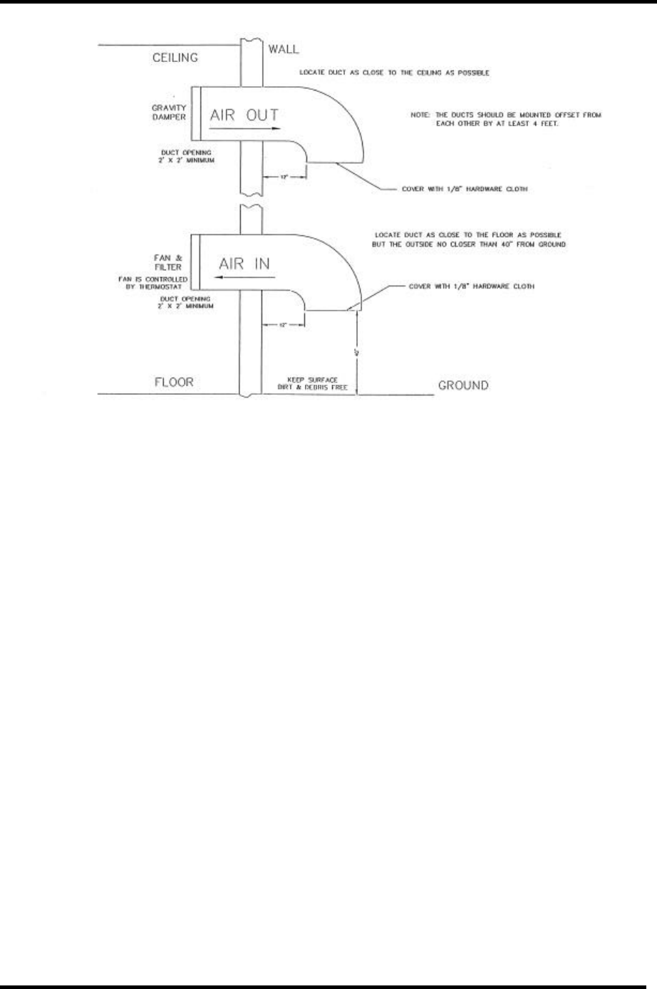
3. The inlet and outlet vents should
be screened with 1/8-inch
hardware cloth (preferred) or
galvanized hardware cloth
(acceptable).
4. Cooling air should enter the room
as low as practical but in no case
higher than four feet above the
floor. The inlet must be located
where dirt, leaves, snow, etc., will
not be carried in with the cooling
air.

2000-Watt VHF Low Band Transmitter Chapter 3, Installation and Setup Procedures
334B, Rev. 0 3-3
5. The exhaust should be located as
high as possible. Some ducting is
usually required to insure the
complete flushing of heated air
with no stagnant areas.
6. The area of the filter, located in
the ducting, must be large enough
to insure a maximum air velocity
of 300 feet per minute through the
filter. This is not a conservative
number but a never-exceed
number. In a dusty or remote
location, this number should be
reduced to 150 CFM.
7. The inlet and outlet(s) must have
automatic dampers that close any
time the ventilation blower is off.
8. In those cases in which
transmitters are regularly off for a
portion of each day, a
temperature-differential sensor
that controls a small heater must
be installed. This sensor will
monitor inside and outside
temperatures simultaneously. If
the inside temperature falls to
within 5° F of the outside
temperature, the heater will come
on. This will prevent condensation
when the ventilation blower comes
on and should be used even in the
summer.
9. A controlled-air bypass system
must be installed to prevent the
temperature in the room from
falling below 40° F during
transmitter operation.
10. The blower should have two
speeds, which are thermostatically
controlled, and also be interlocked
with the transmitter.
11. The blower on high speed must be
capable of moving the required
volume of air into a half inch of
water pressure at the required
elevation. The free air delivery
method must not be used.
12. Regular maintenance of the filters,
if used, can not be
overemphasized.
13. It is recommended that a site plan
be submitted to Axcera for
comments before installation
begins.
In calculating the blower requirements,
filter size, and exhaust size, if the total
load is known in watts, 2000 CFM into ½
inch of water will be required for each
5000 watts. If the load is known in
BTUs, 2000 CFM into ½ inch of water will
be required for each 17,000 BTUs. The
inlet filter must be a minimum of seven
square feet, larger for dusty and remote
locations, for each 5000 watts or 17,000
BTUs. The exhaust must be at least four
square feet at the exhaust screen for
each 5000 watts or 17,000 BTUs.
The information presented in this section
is intended to serve only as a general
guide and may need to be modified for
unusually severe conditions. A
combination of air conditioning and
ventilation should not be difficult to
design (see Figure 3-1). System
interlocking and thermostat settings
should be reviewed with Axcera.
As with any equipment installation, it is
always good practice to consult the
manufacturer when questions arise. The
field support department at Axcera can
be contacted at (724) 873-8100.
2000-Watt VHF Low Band Transmitter Chapter 3, Installation and Setup Procedures
334B, Rev. 0 3-4
Figure 3-1. 1 kW Minimum Ventilation Configuration
3.2 Unpacking the Cabinet and Trays
Note: Air conditioning and any
related heat exhaust ducts should be
in place before continuing with the
installation of the transmitter.
Thoroughly inspect the cabinet and all
other materials upon their arrival.
Axcera certifies that upon leaving our
facility the equipment was undamaged
and in proper working order. The
shipping containers should be inspected
for obvious damage that indicates rough
handling. Check for dents and scratches
or broken switches, meters, or
connectors. Any claims against in-transit
damage should be directed to the carrier.
Inform Axcera as to the extent of any
damage as soon as possible.
Remove the cabinet and the trays from
the crates and boxes. Remove the straps
that hold the cabinet to the shipping skid
and slide the cabinet from the skid.
Remove the plastic wrap and foam
protection from around the cabinet. Do
not remove any labeling or tags from any
cables or connectors; these are
identification markers that make
assembly of the transmitter much easier.
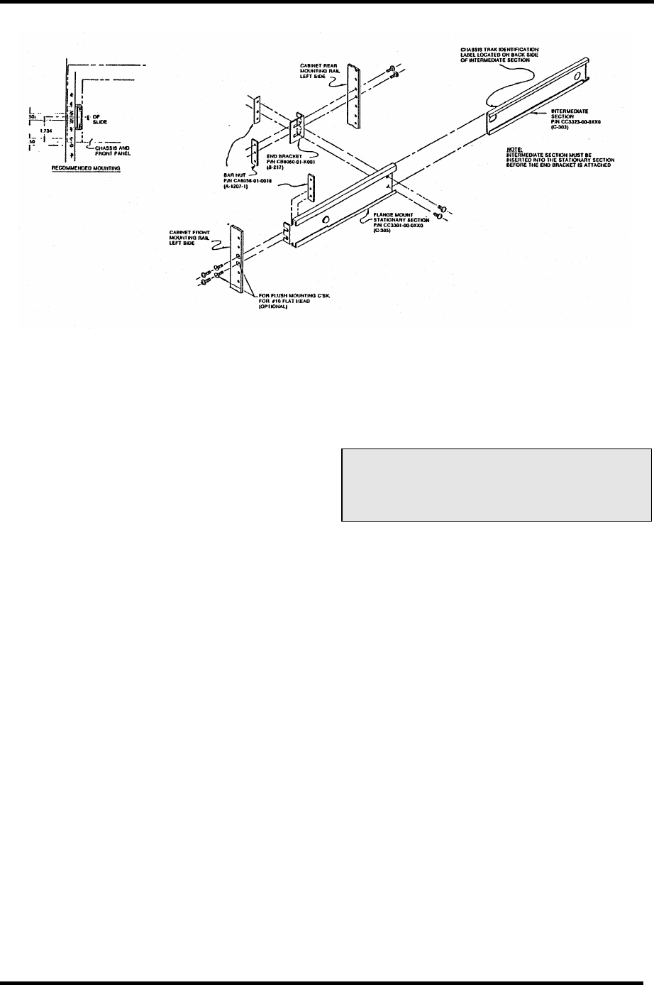
Remove the two L-brackets, mounted on
the front panel rails, which held the trays
in place during shipment. The trays are
mounted in the cabinet using Chassis
Trak cabinet slides as shown in Figure
3-2. The tray slides are on the sides of
the three VHF amplifier trays and the
VHF exciter tray. Inspect the trays for
any loose hardware or connectors,
tightening as needed.
2000-Watt VHF Low Band Transmitter Chapter 3, Installation and Setup Procedures
334B, Rev. 0 3-5
Figure 3-2. Chassis Trak Cabinet Slides
Open the rear door and inspect the
interior of the cabinet for packing
materials and carefully remove any that
are found. Slowly slide each tray in and
out to verify that they do not rub against
each other and have no restrictions to
free movement. It may be necessary to
adjust the position of the trays to keep
them from rubbing. This is accomplished
by loosening the cabinet slide mounting
bolts that hold the front of the slide to
the mounting frame of the cabinet and
moving the tray up or down, as needed,
to correct for the rubbing.
3.3 Installing the Cabinet and Trays
The air intake to the 2000-watt
transmitter is only intended for room air.
The cabinet should be positioned for
adequate air intake and exhaust, the
opening of the rear door, if present;
access to the trays, including sliding
them out for testing, the main AC
hookup, and the installation of the output
transmission line. The cabinet should be
grounded using copper strapping
material and should be permanently
mounted to the floor of the site using the
holes in the bottom of the cabinet.
Once the cabinet is in place, and the
trays are checked for damage, the main
AC hookup can be made.
Caution: Before connecting the 220
VAC, make certain that the circuit
breaker associated with the
transmitter has been switched off.
The main AC input circuit to the 2000-
watt transmitter should be a 25-amp,
220-VAC line, using AWG 10 wire, inside
of a 1-1/4-inch conduit. The three wire
220 VAC input is connected to the AC
distribution block, white to white, black
to black and green to green by stripping
the ends of the wires, approximately ½”,
and placing them into the proper hole
and tightening the retaining screws that
holds them in place. NOTE: The 220VAC
should be connected by a qualified
electrician.
The AC is distributed to the trays through
AC plugs that connect from the power
distribution block to the rear of each tray.
The output of the (A16) coupler assembly
at (A16-J2), which is a 1-5/8” connector
and the RF output for the transmitter,
should connect to the transmission line
for the antenna system.

2000-Watt VHF Low Band Transmitter Chapter 3, Installation and Setup Procedures
334B, Rev. 0 3-6
This completes the unpacking and
installation of the 334B 2000-watt VHF
television transmitter. Refer to the setup
and operation procedures that follow
before applying power to the transmitter.
3.4 Setup and Operation Procedures
Initially, the transmitter should be turned
on with the RF output at (A16-J2) of the
coupler assembly terminated into a
dummy load of at least 2000 watts. If a
load is not available, check that the
output of the coupler assembly is
connected to the antenna.
The baseband audio and video inputs and
any remote control connections must be
made to the (A12) A/V input and remote
interface assembly. The baseband
balanced audio input connects to the
terminal block TB1 or the composite
audio input connects to the BNC jack J6.
Connect the baseband video input to the
BNC jack J2.
NOTE: If your transmitter does not
contain the 4.5 MHz composite input kit,
the following description does not pertain
to your transmitter. The baseband audio
input can remain connected when the
4.5-MHz composite input is in use
without affecting the operation of the
tray. Connect the baseband video input
to BNC jack J2 on the A/V input and the
remote interface assembly. If the
(optional) 4.5-MHz composite input kit is
purchased, connect the 4.5-MHz
composite input to the BNC jack J2. To
use the 4.5-MHz composite input, the
4.5-MHz composite input must be
connected to J2 and the baseband select
must be removed from J7-6 and J7-7 on
the rear of the VHF exciter tray. To use
the baseband video and audio inputs, the
baseband video input must be connected
to J2, the baseband audio must be
connected to the proper jack, and the
baseband select must be connected from
J7-6 and J7-7 on the rear of the VHF
exciter tray.
If the (A12) A/V input and remote
interface assembly is not present in the
system, connections are made directly to
the rear of the VHF exciter tray.
Connect the baseband balanced audio
input to the terminal block TB1 or the
composite audio input to the BNC jack J3
or J13 on the rear of the VHF exciter.
The baseband audio input can remain
connected when using the (Optional) 4.5-
MHz composite input, if present, without
affecting the operation of the tray.
Connect the baseband video input to the
BNC jack J2 or J1 also on the rear of the
VHF exciter or, if the (optional) 4.5-MHz
composite input kit is purchased, connect
the 4.5-MHz composite input to the BNC
jack J2 or J1. To use the 4.5-MHz
composite input, the 4.5-MHz composite
input must be connected to J2 or J1 and
the baseband select must be removed
from J7-6 and J7-7 on the rear of the
tray. To use the baseband video and
audio inputs, the baseband video input
must be connected to J2 or J1, the
baseband audio must be connected to
the proper jack, and a baseband select
must be connected from J7-6 and J7-7.
Switch on the main AC for the
transmitter and the circuit breakers
located on the rear of the VHF exciter,
and on the front of the three VHF
amplifier trays. On the VHF exciter tray,
switch the Operate/Standby switch to
Standby and the Auto/Manual switch to
Manual. Normal operation of the
transmitter is in Automatic, which uses
the video input to the VHF exciter as an
Operate/Standby switch. In Auto, if the
input video is lost for approximately 7
seconds, the transmitter will
automatically revert to Standby and,
when the video signal is restored, the
transmitter will quickly return to Operate.
Move the Operate/Standby switch on the
VHF exciter tray to Operate. This will
apply enables to the switching power
supplies in each of the VHF amplifier
trays. Observe that a power supply
voltage reading of +28 V is on the front

2000-Watt VHF Low Band Transmitter Chapter 3, Installation and Setup Procedures
334B, Rev. 0 3-7
panels of the VHF amplifier trays, in the
power supply position.
NOTE: If the transmitter does not switch
to Operate when the Operate/Standby
switch is placed in Operate, check that on
the (A12) A/V input and remote interface
assembly an external interlock plug is
connected to J9, with a jumper wired
from pins 21 to 22. If the (A12) A/V
input and remote interface assembly is
not present in your transmitter, check
that an external interlock plug is
connected to J11, with a jumper wired
from pins 23 to 24, on the rear of the
VHF exciter.
With the transmitter in Operate, monitor
the front panel meter of the VHF exciter
tray. In the % Visual Power position, it
should read 100%. If necessary, adjust
the screwdriver adjust power pot on the
front panel of the VHF exciter for 100%.
Check the % Reflected Power position. If
the % Reflected Power is very high,
above 10%, a problem exists with the
output coaxial lines and they will need to
be checked. A center bullet missing from
the coax lines or loose bolts on the
connections can cause this problem.
The gain and phase controls on the front
panels of the individual VHF amplifier
trays were adjusted at the factory to
obtain an output of 100% for the
transmitter and should not need to be
readjusted. The front panel readings on
the individual VHF amplifier trays may
not be the same. Refer to the Test Data
Sheet for the transmitter to compare the
final readings from the factory with the
readings on each of the trays after the
setup. If a reading is off by a significant
amount, refer to the phasing and power
adjustment procedures for the VHF
amplifier trays in Chapter 5, Detailed
Alignment Procedures, of this manual
before trying to make any adjustments.
If a dummy load is connected to the
transmitter, switch the unit to Standby
and switch off the main AC circuit
breaker. Remove the dummy load and
make all of the connections that are
needed to connect the transmitter to the
antenna. Switch the main AC circuit
breaker on and the Operate/Standby
switch to Operate. Adjust the output
power screwdriver pot to achieve an
output of 100%.
If the transmitter is already connected to
the antenna, check that the output is
100%. If necessary, adjust the power
screwdriver pot.
This completes the transmitter setup and
operation procedures for the 334B VHF
low band transmitter. The transmitter
can now be operated normally.
If a problem occurred during the setup
and operation procedures, refer to
Chapter 5, Detailed Alignment
Procedures, of this manual for more
information.

2000-Watt VHF Low Band Transmitter Chapter 4, Circuit Descriptions
334B, Rev. 0 4-1
Chapter 4
Circuit Descriptions
4.1 (A4) Low Band VHF Exciter
(1070820 or 1304463 w/P.F.;
Appendix C)
NOTE: The 1304463 VHF Exciter is used
with the precise frequency system and
will contain the VCXO Assembly (1145-
1206), in place of the Channel Oscillator
Assembly (1145-1202), and the IF VCXO
Board (1248-1131), in place of the IF
Oven Oscillator Assembly (1191-1404).
4.1.1 (A4) Aural IF Synthesizer
Board, 4.5 MHz (1265-1303;
Appendix D)
The aural IF synthesizer board amplifies
and controls the levels of the three
possible audio inputs and provides a
single audio output. The balanced audio
or the composite audio input is connected
to the board while the subcarrier audio
(SCA) input can be connected at the
same time as either of the other two
inputs. The board has the 4.5-MHz
voltage-controlled oscillator (VCO) and
the aural modulation circuitry that
produces the modulated 4.5-MHz output.
The board also contains a phase lock loop
(PLL) circuit that maintains the precise
4.5-MHz separation between the aural
(41.25 MHz) and the visual (45.75 MHz)
IF frequencies.
4.1.1.1 Balanced Audio Input
The first of the three possible baseband
audio inputs to the board is a 600Ω-
balanced audio input (+10 dBm low gain
or 0 dBm high gain) that enters through
jack J2, pins 1 (+), 2 (GND), and 3 (-).
The input is then buffered by U1B and
U1C. The diodes CR18 and CR19 are
transient voltage suppressors that
protect the board from any surges or
transients that may occur on the
balanced audio input lines. The Diodes,
CR1 to CR4, protect the input stages of
U1B and U1C if an excessive signal level
is applied to the board. The outputs of
U1B and U1C are applied to the
differential amplifier U1A that eliminates
any common mode signals (hum) on its
input leads. A pre-emphasis of 75 µs is
provided by R11, C11, and R10 and can
be eliminated, if not needed, by
removing the jumper W5 on J5. The
signal is then applied to the amplifier
U1D whose gain is controlled by the
jumper W3 on J11. The Jumper is
positioned according to the input level of
the audio signal (0 or +10 dBm). If the
input level is approximately 0 dBm, the
mini-jumper should be in the high gain
position between pins 1 and 2 of J11. If
the input level is approximately +10
dBm, the mini-jumper should be in low
gain position which is between pins 2 and
3 of J11. The balanced audio is then
connected to the buffer amplifier U2A
whose input level is determined by the
setting of balanced audio gain pot R13.
The output of the amplifier stage is wired
to the summing point at U2D pin 13.
4.1.1.2 Composite Audio Input
The second possible audio input to the
board is the composite audio (stereo)
input at BNC jacks J3 and J13. The two
jacks are loop-through connected.
Therefore, the audio can be used in
another application by connecting to the
unused jack and moving the jumper W4
to J12 between pins 2 & 3. The jumper
W4 on jack J12 provides a 75Ω-input
impedance when the jumper is on J12
pins 1 and 2 and a high impedance when
it is on pins 2 and 3. The diodes CR20
and CR21 are transient voltage
suppressors that protect the board from
surges and transients on the composite
audio input lines. Diodes CR9 to CR12
protect the input stages of U6A and U6B
if an excessive signal level is applied to
the board. The outputs of U6A and U6B
are connected to the differential amplifier
U2C, which eliminates any common

2000-Watt VHF Low Band Transmitter Chapter 4, Circuit Descriptions
334B, Rev. 0 4-2
mode signals (hum) that may occur on
its input leads. The composite audio
input signal is applied to the amplifier
U2B whose gain is controlled by the
composite audio gain pot R17. The
composite audio signal is then connected
to the summing point at U2D pin 13.
4.1.1.3 Subcarrier Audio Input
The third possible input to the board is
the subcarrier audio (SCA) input at the
BNC jack J4. The SCA input has an input
impedance of 75Ω that can be eliminated
by removing the jumper W2 from J14.
The SCA input is bandpass filtered by
C66, C14, R22, C15, C67, and R23 and
fed to the buffer amplifier U3A pin 3.
The amplified signal is then applied
though the SCA gain pot R24 to the
summing point at pin 13 of U2D.
4.1.1.4 Audio Modulation of the VCO
The balanced audio or the composite
audio and/or the SCA audio signals, are
fed to the common junction of resistors
R14, R20, and R27 that connect to the
summing point at pin 13 of the amplifier
U2D. The output audio signal at pin 14
of U2D is typically .8 Vpk-pk at a ±25-
kHz deviation with a balanced audio input
or .8 Vpk-pk at ±75-kHz deviation with a
composite audio input, as measured at
TP1. This audio signal is applied to the
VCO U10. A sample of the deviation
level is amplified, detected by U7A and
U7B, and connected to J10 on the board,
which is cabled to the front panel meter
through the transmitter control board.
The audio is applied through C64, a
frequency response adjustment, to CR13
to CR16, which are varactor diodes that
frequency modulate the audio signal onto
the generated 4.5-MHz signal in U10.
U10 is the 4.5-MHz VCO that generates
the 4.5-MHz continuous wave (CW)
signal. The output frequency of this
signal is maintained and controlled by the
correction voltage output of the PLL IC
U5. The audio-modulated, 4.5-MHz
signal is fed to amplifiers U11A and
U11B. The output of U11B is connected
to the 4.5-MHz output jacks at J7 and J8.
4.1.1.5 Phase Lock Loop (PLL) Circuit
A sample of the signal from the 4.5-MHz
aural VCO at the output of U11A is
applied to the PLL IC U5 pin 1, the Fin
connection. In U5, the signal is divided
down to 50 kHz and is compared to a 50-
kHz reference signal. The 50-kHz
reference signal is a divided-down
sample of the visual IF, 45.75-MHz signal
generated on the IF carrier oven
oscillator board, that is applied to pin 27,
the oscillator in connection, on the PLL
chip through jack J6 on the board. These
two 50-kHz signals are compared in the
IC and the fV
output at pin 8 and the fR
output at pin 7 are applied to the
differential amplifier U3B. The output of
U3B is fed back through CR17 to the 4.5-
MHz VCO IC U10, which sets up a PLL
circuit, therefore any change in frequency
will be corrected by the AFC error
voltage. The 4.5-MHz VCO, using the
PLL circuit, will maintain the extremely
accurate 4.5-MHz separation between the
visual 45.75 MHz and aural 41.25 MHz IF
signals.
The PLL chip U5 also contains an internal
lock detector that indicates the status of
the PLL circuit. When U5 is in a "locked"
state, pin 28 goes high and causes the
green LED DS1 to illuminate. If the 4.5-
MHz VCO and the 45.75-MHz oscillator
become "unlocked," out of the capture
range of the PLL circuit, pin 28 of U5 will
go to a logic low and cause the red LED
DS2 to light. A mute output signal from
Q3 (unlock mute) will be applied to jack
J9. This mute is connected to the
transmitter control board.
4.1.1.6 Voltage Requirements
The ±12 VDC needed for the operation of
the board enters through jack J1. The
+12 VDC is connected to J1-3 and
filtered by L2, C3, and C4 before it is
connected to the rest of the board. The

2000-Watt VHF Low Band Transmitter Chapter 4, Circuit Descriptions
334B, Rev. 0 4-3
-12 VDC is connected to J1-5 and filtered
by L1, C1, and C2 before it is connected
to the rest of the board. Two
connections of the +12 VDC are to U8
and U9, which are 5-volt regulator ICs
that provide the voltage to the U10 and
U5 ICs.
4.1.2 (A5) Sync Tip Clamp/
Modulator Board (1265-1302;
Appendix D)
The sync tip clamp/modulator board is
divided into five circuits: the main video
circuit, the sync tip clamp circuit, the
visual modulator circuit, the aural IF
mixer circuit, and the diplexer circuit.
The sync tip clamp/modulator board
takes the baseband video or the 4.5-MHz
composite input that is connected to the
video input jack, either J1 or J2, which
are loop-through connected, and
produces a modulated visual IF + aural
IF output at output jack J20 on the
board. The clamp portion of the board
maintains a constant peak of sync level
over varying average picture levels
(APL). The modulator portion of the
board contains the circuitry that
generates an amplitude modulated
vestigial sideband visual IF signal output
that is made up of the baseband video
input signal (1 Vpk-pk) modulated onto
an externally generated 45.75-MHz IF
carrier frequency. The visual IF signal
and the aural IF signal are combined in
the diplexer circuit to produce the visual
IF + aural IF output that is connected to
J20, the IF output jack of the board.
4.1.2.1 Main Video Signal Path (Part 1 of
2)
The baseband video or the 4.5-MHz
composite input connects to the board at
J2. J2 is loop-through connected to J1
and terminated into 75Ù, if the jumper
W4 is on jack J3. With jumper W4
removed, the input can be connected to
another transmitter through J1.
Test point TP1 is provided to monitor the
level of the input. The input is fed to the
non-inverting and inverting inputs of
U1A, a differential amplifier that
minimizes any common-mode hum that
may be present on the incoming signal.
Diodes CR1 to CR4 form a voltage-limiter
network in which, if the input voltages
exceed the supply voltages for U1A, the
diodes conduct, preventing damage to
U1A. CR1 and CR3 conduct if the input
voltage exceeds the negative supply and
CR2 and CR4 conduct if the input voltage
exceeds the positive supply voltage.
The video output of U1A is connected to
J22 on the board. Normally, the video at
J22 is jumpered to J27 on the board. If
the optional 4.5-MHz composite input kit
is purchased, the 4.5-MHz composite
signal at J22 connects to the external
composite 4.5-MHz filter board and the
4.5-MHz bandpass filter board. These
two boards provide the video-only signal
to J27 and the 4.5-MHz intercarrier signal
to J28 from the 4.5-MHz composite input.
The video through the video gain pot R12
is typically adjusted for 1 Vpk-pk at TP2
and connects to amplifier U1B.
The output of U1B, if the delay equalizer
board is present in the tray, connects the
video from J6 pin 2, to the external delay
equalizer board and back to the sync tip
clamp/modulator board at J6 pin 4. If
the delay equalizer is not present, the
video connects through jumper W1 on J5,
pins 1 and 2. The delay equalizer board
plugs directly into J6 on the sync tip
clamp/modulator board. The video from
J6 pin 4 is connected through the jumper
W1 on J5 pins 2 and 3, to the amplifier
Q1. The output of Q1 connects to Q2.
The base voltage of Q2 is set by the DC
offset voltage output of U3B, which is the
sync tip clamp circuit output.
4.1.2.2 Sync Tip Clamp Circuit
The automatic sync tip clamp circuit is
made up of U4A, Q7, U3B, and
associated components. The circuit
begins with a sample of the clamped

2000-Watt VHF Low Band Transmitter Chapter 4, Circuit Descriptions
334B, Rev. 0 4-4
video that is split off from the main video
path at the emitter of Q3. The video
sample is buffered by U3A and connected
to U4A. The level at which the tip of sync
is clamped, approximately -1.04 VDC, as
measured at TP2, is set by the voltage-
divider network connected to U4A. If the
video level changes, the sample applied
to U4A changes. If the jumper W7 on J4
is in the Clamp-On position, the voltage
from the clamp circuit that is applied to
the summing circuit at the base of Q2 will
change and bring the sync tip level back
to approximately -1.04 VDC. Q7 will be
turned off and on by the peak of sync
voltage level that is applied to U4A. The
capacitors C14, C51, C77, and C41 will
charge or discharge to the new voltage
level, which biases U3B more or less,
through the jumper W7 on J4 when in
the Auto Clamp-On position. U3 will
increase or decrease its output, as
needed, to bring the peak of sync back to
the correct level that is set by R152 and
R12. This voltage level is applied
through U3B to Q2. In the Manual
position, jumper W7 on J4 is in the
Clamp-Off position, between pins 1 and
2, and the adjustable resistor R41
provides the manual clamp bias
adjustment for the video that connects to
Q2.
The Jumper W6 on jack J35 must be in
the Normal position, between pins 2 and
3, for the clamp circuit to operate with a
normal non-scrambled signal. If a
scrambled signal is used, the tray is
operated with jumper W6 in the Encoded
position, connected between pins 1 and
2.
The clamp circuit is set by adjusting the
depth of modulation pot R152 for the
correct depth of modulation as measured
at TP2. Depending on the input video
level, the waveform as measured at TP2
may not be 1 Vpk-pk. If W7 on J4 is
moved to the Clamp-Off (Manual)
position, between pins 1 and 2, the
clamp level is adjusted by R41 and will
not automatically be clamped to the set
level.
The output of buffer amplifier U3A drives
the sync tip clamp circuit consisting of
the differential amplifier U4A, FET Q7,
and buffer amplifier U3B. U4A is biased
by R124, R125, R184, R152, and R126
so that the clamped voltage level at the
peak of sync is approximately -1.04 VDC
as measured at TP2.
4.1.2.3 Main Video Signal Path (Part 2 of
2)
The clamped video from Q2 is connected
to the white clipper circuit Q3. Q3 is
adjusted by R20 and set to prevent video
transients from overmodulating the video
carrier. The clamped video is connected
to the sync clipper circuit Q4, which is
adjusted by R24. Q4 limits the sync to
-40 IRE units. The corrected video
output of the emitter follower Q4 is wired
to the unity gain amplifier U2A that
provides a low impedance, clamped video
output at pin 1, which can be measured
at TP2.
4.1.2.4 Visual Modulator Circuit
The clamped video signal from U2A is
split. One part connects to a metering
circuit, consisting of U20 and associated
components, which produces a video
output sample, white level, at J8-6 that
connects through the transmitter control
board to the front panel meter for
monitoring. The other clamped video
path from U2A is through a sync stretch
circuit that consists of Q5 and Q6. The
sync stretch circuit contains R48 that
adjusts the sync stretch magnitude
(amount) and R45 that adjusts the cut-in
point. This sync stretch adjustment
should not be used to correct for output
sync problems, but it can be used for
input video sync problems. The output of
the sync stretch circuit connects to pin 5,
the I input of mixer Z1.
The video signal is heterodyned, in mixer
Z1, with the 45.75 MHz visual IF CW
signal. The visual IF CW signal enters
the board at jack J15 and is connected to
U9, where it is amplified and wired to pin

2000-Watt VHF Low Band Transmitter Chapter 4, Circuit Descriptions
334B, Rev. 0 4-5
1, the L input of mixer Z1. The
adjustable capacitor C78 and resistor R53
are set up to add a small amount of
incidental carrier phase modulation
(ICPM) correction to the output of the
mixer stage to compensate for any non-
linearities generated by the mixer.
The modulated 45.75-MHz RF output of
mixer Z1, at pin 4, the R output, is
amplified by U5 and is fed to J18 the
double sideband visual IF output jack.
The level at this output jack is adjusted
by R70, typically –4 to –10 dBm. J18 is
the visual IF loop-through output jack
that is normally jumpered by W10 to J19
on the board. If the (Optional) visual IF
loop-through kit is purchased, the visual
is connected out of the board to any
external IF processor trays and then back
to the board.
After any external processing, the
modulated visual IF, double-sideband
signal re-enters the board through J19.
The visual IF from J19 is amplified by
U10 and U11 and routed through the
vestigial sideband filter network,
consisting of T1, FL1, and T2, that
produces a vestigial sideband visual IF
signal output. The filtered vestigial
sideband visual IF is amplified by U7 and
connected to a T-type attenuator. R62 is
adjustable to set the visual IF gain, which
is the amount of visual IF signal that is
coupled to the amplifier IC U8. R63 and
C30 are adjusted for the best VSBF
frequency response. The amplified IF
signal output of U8 is fed to the input of
the diplexer circuit that consists of R76,
L13, and L12. A detected voltage sample
of the visual IF is available at the test
point TP5.
4.1.2.5 41.25-MHz Aural IF Circuit
The modulated 41.25-MHz aural IF is
created on this board by mixing the
modulated 4.5-MHz aural intercarrier
signal, produced by the aural IF
synthesizer board or by the optional
composite 4.5-MHz filter board, with the
45.75-MHz CW signal produced by the
45.75-MHz IF carrier oven oscillator
board or the IF VCXO board, in a precise
frequency system. The modulated
baseband 4.5-MHz aural intercarrier
signal enters the board at J14, baseband
4.5-MHz Input, and for normal operation
connects through the jumper W8 on J32
pins 1 and 2, IF Relay Disabled, through
the jumper W3 on J7 pins 2 and 3,
Internal 4.5-MHz, to Z2 pin 5, the I input
of the Mixer.
If both composite 4.5-MHz and baseband
4.5-MHz is to be used in your system,
then the relay K1 must be enabled. This
is accomplished by moving the jumper
W8 on J32 to between pins 2 and 3.
Both inputs, the modulated baseband
4.5-MHz aural intercarrier input from J14
and the Composite 4.5-MHz Input from
J28 connect to the IF relay K1. The
jumper W2 on J30 must be between pins
1 and 2, baseband select off, for external
operation of the relay. Now the relay is
controlled by a baseband select, Low,
that connects to J31 Pin 3. With the
baseband select, Low, present at J31 pin
3, the relay is energized and applies the
baseband 4.5 MHz to the mixer Z2 and
DS1 the baseband indicator will be lit.
With the baseband select removed, not
present at J31 pin 3, the relay is de-
energized and applies the composite 4.5
MHz to the mixer Z2 and DS1 the
baseband indicator will not be lit.
The Jumper W3 on J7 determines
whether the 4.5-MHz used by the board
is internally generated, either the
baseband or composite inputs, or from
an external source. With the jumper W3
connected between pins 2 and 3, the 4.5
MHz from the aural IF synthesizer board
or from the 4.5-MHz composite input is
connected to the mixer Z2. With the
jumper W3 connected between pins 1
and 2, the external 4.5 MHz input is
connected to the mixer Z2. The external
4.5-MHz signal enters the board at J12
and is fed through the gain pot R88 to
the amplifier IC U13A. The amplified 4.5-
MHz is then connected to J7 through the
jumper W3 to the mixer.

2000-Watt VHF Low Band Transmitter Chapter 4, Circuit Descriptions
334B, Rev. 0 4-6
The Mixer Z2 heterodynes the aural-
modulated, 4.5-MHz signal with the
45.75-MHz CW signal to produce the
modulated 41.25-MHz aural IF signal
output.
The output of the mixer at pin 4, the R
output, is fed to a bandpass filter that is
tuned to pass only the modulated 41.25-
MHz aural IF signal. The bandpass
filtered signal is fed to jack J16, the
41.25-MHz aural IF loop-through output
jack of the board. For normal operation,
the 41.25-MHz signal is jumpered by a
coaxial cable W11 from J16 to J17 on the
board. If the (Optional) aural IF loop-
through kit is purchased, the Aural IF
41.25-MHz signal is connected to the rear
of the tray, to which any Aural IF
processing trays can be connected, and
then back to jack J17 on the board.
The modulated 41.25-MHz aural IF signal
from J17 is connected through an
impedance matching transformer T3,
75Ù to 50Ù, to the amplifier ICs U15 and
U16. The amplified output is connected
to the attenuator matching circuit that is
adjusted by R85. R85 increases or
decreases the level of the Aural IF 41.25
MHz that sets the A/V ratio in the
diplexer circuit.
4.1.2.6 Diplexer Circuit
The diplexer circuit takes the modulated
45.75-MHz visual IF, that connects to the
junction of R76 and L12, and the
modulated 41.25-MHz aural IF, that
connects to the junction of R76 and L13,
and combines them to produce the
45.75-MHz + 41.25-MHz IF output. The
combined 45.75-MHz + 41.25-MHz IF
signal is amplified by U12 and connected
to J20 the combined IF output jack of the
board. A sample of the combined IF
output is provided at J21.
If an (Optional) NICAM input is used, it
connects to J36 on the board. The level
of the NICAM signal is set by R109 before
it is fed to the diplexer circuit consisting
of L28, L29, and R115. This circuit
combines the NICAM signal with the
45.75-MHz visual IF + 41.25-MHz aural
IF signal.
4.1.2.7 Operational Voltages
The +12 VDC needed to operate the sync
tip clamp modulator board enters the
board at J23 pin 3, and is filtered by L26,
L33, and C73 before it is connected to
the rest of the board.
The -12 VDC needed to operate the
board enters the board at J23 pin 5, and
is filtered by L27 and C74 before being
fed to the rest of the board.
4.1.3(Optional) (A6) Delay Equalizer
Board (1227-1204; Appendix D)
The (Optional) delay equalizer board
provides a delay to the video signal,
correction to the frequency response, and
amplification of the video signal.
The video signal enters the board at J1-2
and is connected to a pi-type, low-pass
filter consisting of C16, L7, and C17.
This filter eliminates any unwanted
higher frequencies from entering the
board. The output of the filter is
connected to the amplifier stage U1,
whose gain is controlled by R29. The
video output of the amplifier stage is
wired to the first of four delay-equalizing
circuits that shape the video signal to the
FCC specification for delay equalization or
to the desired shape needed for the
system. The board has been factory-
adjusted to the FCC specification and
should not be readjusted without the
proper equipment.
Resistors R7, R12, R17, and R22 adjust
the sharpness of the response curve,
while inductors L1, L2, L3, and L4 adjust
the position of the curve. With a delay
equalizer test generator signal or a sine
x/x video test pattern input, the resistors
and inductors can be adjusted, while
monitoring a Tektronix VM700 test
measurement set, until the desired FCC
delay equalization curve or system curve

2000-Watt VHF Low Band Transmitter Chapter 4, Circuit Descriptions
334B, Rev. 0 4-7
is attained. The delay-equalized video
signal output of the board is at J1-4. A
sample of the delayed video signal is
provided at J2 on the board and can be
used for testing purposes.
The ±12 VDC needed to operate the
board enters the board at J1. The +12
VDC connects to J1-9, which is filtered by
L5 and C11 before it is directed to the
rest of the board. The -12 VDC connects
to J1-6, which is filtered by L6 and C12
before it is directed to the rest of the
board.
4.1.4 (A7) IF Carrier Oven Oscillator
Board (1191-1404; Appendix D)
NOTE: If the precise frequency kit is
present in your transmitter, the IF VCXO
Board (1248-1131) will be used.
The IF carrier oven oscillator board
generates the visual IF CW signal at
45.75 MHz for NTSC system "M" usage.
The 45.75 MHz crystal Y1 is the principal
device that determines the operating
frequency and is the most sensitive in
terms of temperature stability, therefore
it is enclosed in an oven. +12 VDC is
applied through jack J10 to the crystal
oven HR1, which is preset to operate at
60° C. The oven encloses the crystal Y1
and stabilizes the crystal temperature.
The crystal operates in an oscillator
circuit consisting of the transistor Q1 and
its associated components. Feedback is
provided through a capacitor voltage
divider, consisting of C5 and C6, that
operates the crystal in a common-base
amplifier configuration using Q1. The
operating frequency of the oscillator can
be adjusted by the variable capacitor
C17. The oscillator circuit around Q1 has
a separate regulated voltage, 6.8 VDC,
which is produced from the +12 VDC by
a combination of the dropping resistor R4
and the zener diode VR1. The output of
the oscillator at the collector of Q1 is
capacitively coupled through C8 to the
base of Q2. The small value of C8, 10
pF, prevents the oscillator from being
loaded down by Q2.
Q2 is operated as a common-emitter
amplifier stage whose bias is provided
through R8 from the +12 VDC line. The
output of Q2, at its collector, is split
between two emitter-follower transistor
stages, Q3 and Q4. The output of Q3 is
taken from its emitter through R11, to
establish an approximate 50-ohm source
impedance, through C11 to J3, the main
output jack of the board. This 45.75-
MHz signal is approximately +5 dBm in
level. The output is directed to a visual
modulator circuit located on the
clamp/modulator board. The second
output from the collector of Q2 is fed to
the base of Q4, an emitter follower
transistor. Q4 drives two different output
circuits. One output is directed through
the voltage dividers R14 and R15 to jack
J2 and is normally fed to a frequency
counter. While monitoring J2 the
oscillator can be set exactly on the
operating frequency (45.75 MHz) by
adjusting C17. The output at J2 is
approximately -2 dBm in level, which is
sufficient to drive most frequency
counters. The other output of Q4
connects to the prescaler chip U1, which
divides the signal by 15. The output of
U1 is applied to U2, a programmable
divider IC. U2 is programmed through
pins 11 to 20 to divide by 61, which
results in a 50-kHz signal at pin 9 that is
available as an output at J1. This 50 kHz
reference output is generally used in
systems where the visual IF carrier oven
oscillator is used as the reference for a
PLL circuit. An example of this is when
the PLL circuit locks the aural VCO on the
aural IF synthesizer board. The 50-kHz
CMOS output at jack J1 is not capable of
achieving enough drive level for a long
coaxial cable length. As a result, when a
long coaxial cable is needed, the output
at jack J5 is utilized. The push-pull
transistor stage Q5 and Q6, along with
emitter resistor R18, provide a large load
output capability at J5.

2000-Watt VHF Low Band Transmitter Chapter 4, Circuit Descriptions
334B, Rev. 0 4-8
The stages U1, U2, U3, Q5, and Q6 are
powered by +5.1 VDC, which is obtained
from the +12 VDC line voltage using the
voltage-dropping resistor R16 and the
zener diode VR2.
The +12 VDC input to the board is
applied through the jack J4 at pin 3. The
voltage is isolated from any RF, which
may occur in the +12 VDC line, through
the use of the RF choke L2 and the filter
capacitor C10.
4.1.4.1 (Optional) (A7) IF VCXO
Board (1248-1131; Appendix D)
NOTE: If a precise frequency kit is not
present in your transmitter, the IF Carrier
Oven Oscillator Board (1191-1404) will
be used.
The IF Carrier VCXO Board generates the
Visual IF CW signal at 45.75 MHz for
NTSC System "M" usage.
The 45.75 MHz crystal Y1 is the principal
device that determines the operating
frequency and is the most sensitive in
terms of temperature stability, therefore
it is enclosed in an oven. +12 VDC is
applied through jack J10 to the crystal
oven HR1, which is preset to operate at
60° C. The oven encloses the crystal Y1
and stabilizes the crystal temperature.
The crystal operates in an oscillator
circuit consisting of the transistor Q1 and
its associated components. Feedback is
provided through a capacitor voltage
divider, consisting of C5 and C6, which
operates the crystal in a Common Base
Amplifier configuration using Q1. The
operating frequency of the Oscillator is
adjustable by the variable capacitor C22
and maintained for accuracy by the AFC
voltage, from the external Precise
Frequency Tray, that connects to J13.
The AFC voltage input connects through
J13 and then the combination of the
dropping resistor R23 and the Zener
Diode VR1 to the oscillator circuit. The
output of the oscillator at the collector of
Q1 is capacitively coupled through C8 to
the base of Q2. The small value of C8,
10 pF, prevents the oscillator from being
loaded down by Q2.
Q2 is operated as a Common Emitter
Amplifier stage whose bias is provided
through R8 from the +12 VDC line. The
output of Q2, at its collector, is split
between two Emitter Follower Transistor
Stages, Q3 and Q4. The output of Q3 is
taken from its Emitter through R11 to
establish an approximate 50Ù source
impedance thru C11 to J3 the Main
Output Jack of the board. The 45.75
MHz signal is approximately +5 dBm in
level. A Sample of the Main O/P is
provided at J11. The second output
from the collector of Q2 is fed to the
Base of the Emitter Follower Transistor,
Q4.
Q4 drives two different output circuits.
One output is directed through a voltage
divider R14 and R15 to Jack J2 that is
typically fed to a Frequency Counter.
The output level at J2 is approximately
-2 dBm, which is sufficient to drive most
Frequency Counters. The other output of
Q4 connects to (U1) a Prescaler Chip that
divides the signal by 15. The output of
U1 is applied to (U2) a Programmable
Divider IC. U2 is programmed through
Pins 11-20 to divide by 61, which results
in a 50 kHz signal at Pin 9 that is
available as an output at J1. The output
of 50 kHz is generally used in systems
where the Visual IF Carrier Oven
Oscillator is used as the reference for a
PLL Circuit. An example is the PLL Circuit
using the Aural IF Synthesizer Board and
the Aural VCO. The 50 kHz CMOS Output
at Jack J1 is not capable of enough drive
level for a long coaxial cable length,
therefore, when a long coaxial cable is
needed, the output at Jack J5 is utilized.
The Push-Pull transistor stage Q5 and
Q6, along with the Emitter resistor R18,
provide a large load output capability at
J5.
The stages U1, U2, U3, Q5 and Q6 are
powered by +5.1 VDC, which is obtained
from the +12 VDC line voltage and the

2000-Watt VHF Low Band Transmitter Chapter 4, Circuit Descriptions
334B, Rev. 0 4-9
voltage dropping resistor R16 and Zener
Diode VR2.
The +12 VDC input to the board is
applied through Jack J4 Pin 3 and is
isolated from any RF, which may occur
on the +12 VDC Line, through the use of
the RF choke L2 and the filter capacitor
C10.
4.1.5 (A8) ALC Board, NTSC (1265-
1305; Appendix D)
The automatic level control (ALC) board
provides the ALC and amplitude linearity
correction of the IF signal. The ALC
adjusts the level of the IF signal through
the board to control the output power of
the transmitter.
The visual + aural IF input (0 dBm)
signal, from the clamp/modulator board,
enters the board at the modulator IF
input jack J32. If the (Optional) receiver
tray is present, the visual + aural IF
input (0 dBm) from the receiver tray
connects to receiver IF input jack J1.
4.1.5.1 Local Modulator Select Enabled
(Normal Operation with the Modulator IF
as the Input)
The modulator IF input connects to the
relay K3 and the receiver IF input
connects to the relay K4. The two relays
are controlled by the position of the local
Modulator Select enable/disable jumper
W11 on J29. The normal operation of
the transmitter uses the Modulator IF
input at J32. The jumper W11 connected
between pins 2 and 3 is the normal
operating position for the board. This
sets the board to the local Modulator
enable position, which is both relays de-
energized and the Modulator IF Input
connected to the rest of the board. DS5
the Modulator Enable LED will be lit.
4.1.5.2 Local Modulator Select Disabled
(Operation with the ability to select either
the Modulator IF or the Receiver IF as
the Input)
If a receiver tray is part of your system,
then the relays need to be controlled by
the Modulator Select command that is
connected to J30 on the board, so that
either the receiver IF or the modulator IF
can be used by the board. The position
of the Modulator select enable/disable
jumper W11 on J29 provides for the
Modulator Select command at J30 to
control the operation of the relays. With
the jumper W11 on J29, between pins 1
and 2, the Modulator Select command at
J30 controls the operation of the relays
and with the jumper W11 on J29,
between pins 2 and 3, the modulator is
selected all of the time and DS5, the
modulator enable LED, will be lit.
4.1.5.3 Modulator IF Selected
(With the Local Modulator Select
Disabled)
The modulator is normally selected by
J11-10 and J11-28 on the rear of the VHF
exciter tray, wired to J30 on the board,
connected together. This makes J30 go
low and causes relays K3 and K4 to de-
energize. When K4 is de-energized, it
connects the receiver IF input at J1 to
50Ù. When K3 is de-energized, it
connects the modulator IF input at J32 to
the rest of the board and the Modulator
Enable LED DS5 will be illuminated.
4.1.5.4 Receiver IF Selected
(With the Local Modulator Select
Disabled)
The receiver is normally selected when
J11-10 and J11-28 on the rear of the VHF
exciter tray, connected to J30 on the
board, are not connected together. This
makes J30 high and causes the relays K3
and K4 to energize. When K4 is
energized, it connects the receiver IF
input at J1 to the rest of the board.
When K3 is energized, it connects the
modulator IF input at J32 to 50Ù and the
Modulator Enable LED DS5 will not be
illuminated.

2000-Watt VHF Low Band Transmitter Chapter 4, Circuit Descriptions
334B, Rev. 0 4-10
4.1.5.5 Main IF Signal Path (Part 1 of 3)
The selected visual + aural IF input (0
dBm) signal is split at L1 and L2, with
one half of the signal flowing through L1
and entering a bandpass filter that
consists of L3, L4, C4, L5, and L6. This
bandpass filter can be tuned with C4 and
is substantially broader than the IF signal
bandwidth. It is used to slightly steer the
frequency response of the IF to make up
for any small discrepancies in the
frequency response in the stages that
precede this point. The filter also serves
the additional function of rejecting
unwanted frequencies that may occur if
the tray cover is off and the tray is in a
high RF environment. If this is the case,
the transmitter will have to be serviced
with the tray cover off in spite of the
presence of other RF signals. The filtered
IF signal is fed through a pi-type
matching pad consisting of R2, R3, and
R4 to the pin-diode attenuator circuit
consisting of CR1, CR2, and CR3.
4.1.5.6 Input Level Detector Circuit
The other part of the split IF input is
connected through L2 and C44 to U7, an
IC amplifier that is the first stage of the
input level detector circuit. The amplified
IF is fed to T4 that is a step-up
transformer, which feeds a diode
detector CR14. The positive-going
detected signal is then low-pass filtered
by C49, L18, and C50. This allows only
the video with positive sync to be applied
through the emitter follower Q1. The
signal is then connected to the detector
CR15 that produces a peak of sync
voltage, which is applied to the op-amp
U9A. There is a test point at TP3 that
provides a voltage reference check of the
input level. The detector serves the dual
function of providing a reference that
determines the input IF signal level to
the board and also serves as an input
threshold detector. The input threshold
detector prevents the automatic level
control from reducing the attenuation of
the pin-diode attenuator to minimum
(the maximum signal) if the IF input to
the board is removed. Without the
threshold detector, and with the pin-
diode attenuator at minimum, when the
signal is restored it will overdrive the
stages following this board. The ALC,
video loss cutback, and the threshold
detector circuits will only operate when
jumper W3 on jack J6 is in the Auto
position, between pins 1 and 2.
As part of the threshold detector
operation, the minimum IF input level, as
measured at TP3, is fed through the
detector diode CR15 to the op-amp IC
U9A pin 2. The reference voltage for the
op-amp is determined by the voltage
divider that consists of R50 and R51, off
the +12 VDC line. When the detected
input signal level at U9A pin 2, falls
below this reference threshold,
approximately 10 dB below the normal
input level, the output of U9A at pin 1
goes to the +12 VDC rail. This high is
connected to the base of Q2. At this
point, Q2 is forward biased and creates a
current path from the -12 VDC line
through the red LED DS1, the input level
fault indicator, which lights, the resistor
R54, and the transistor Q2 to the +12
VDC line.
The high from U9A also connects through
the diode CR16 to U9B pin 5, whose
output at pin 7 goes high. The high
connects through the range adjust pot
R74 to J20, which connects to the front
panel mounted power adjust pot. This
high also connects to U10A pin 2, and
causes it to go low at U10A pin 1. The
low is applied through the jumper W3 on
J6, when in auto, to the pin-diode
attenuator circuit, CR1 – CR3, that cuts
back the IF level and, therefore also the
output power level, to 0. When the input
signal level increases above the threshold
level, the output power will increase, as
the input level increases, until normal
output power is reached.
The video input level as measured at TP3
is also fed to a sync-separator circuit,
consisting of U8, CR17, Q3, and
associated components, and then to a

2000-Watt VHF Low Band Transmitter Chapter 4, Circuit Descriptions
334B, Rev. 0 4-11
comparator circuit made up of U9C and
U9D. The reference voltage for the
comparators is determined by a voltage
divider network consisting of R129, R64,
R65, R66, and R130, off the -12 VDC
line. When the input signal level falls
below this reference threshold, which
acts as a loss of sync detector circuit, the
outputs of U9C and U9D move towards
the -12 VDC rail. The low output is split
with one part connecting to and biasing
on the transistor Q5. A current path is
then established from the +12 VDC line
through Q5, the resistors R69, R137, and
the red LED DS3, the video loss indicator,
which lights. When Q5 is biased on, it
applies a high to the gates of Q6 and Q7.
This causes them to conduct and apply
video loss fault pull-down outputs to J18
pins 5 and 2.
The other low output of U9C and U9D is
connected through CR20 to jack J5,
which controls the cutback enable/disable
operation. The jumper W2 on J5, in the
Cutback Enable position, which is
between pins 2 and 3, connects the low
to the base of Q4 that is forward-biased.
If the jumper W2 is in the Disable
position, between pins 1 and 2, the auto
cutback will not operate. With Q4 biased
on, a level determined by the setting of
the cutback level pot R71, which is set at
the factory to cut back the output to
approximately 25%, is applied to U9B pin
5. The output of U9B at pin 7 goes low
and is applied through the power adjust
pot to U10A pin 2, whose output goes
low. This low is applied to the pin-diode
attenuator, CR1-CR3, to cut back the
level of the output to the cut back value
of approximately 25%.
4.1.5.7 Pin-Diode Attenuator Circuit
The input IF signal to the board is fed to
a pin-diode attenuator circuit that
consists of CR1, CR2 & CR3. Each of the
pin diodes contains a wide intrinsic
region, which makes the diodes function
as voltage variable resistors at this
intermediate frequency. The value of the
resistance is controlled by the DC bias
applied to the diodes. The pin diodes are
configured in a pi-type attenuator
configuration where CR1 is the first shunt
element, CR3 is the series element, and
CR2 is the second shunt element. The
control voltage, which can be measured
at TP1, originates either from the ALC
circuit, when jumper W3 on J6 is in the
ALC Auto position, between pins 1 and 2,
or from the variable resistor R87 when
the jumper is in the Manual Gain
position, between pins 2 and 3. In the
pin-diode attenuator circuit, a current
path exists from J6 through R6 and then
through the diodes of the pin attenuator.
Changing the amount of current through
the diodes by forward biasing them,
decreases their resistances which
increases the IF output level of the
board.
There are two extremes of attenuation
ranges for the pin-diode attenuators. In
the minimum attenuation case, the
voltage, as measured at TP1, approaches
the +12 VDC line. There is a current
path created through R6, through series
diode CR3, and finally through R9 to
ground. This path forward biases CR3
and causes it to act as a relatively low-
value resistor. In addition, the larger
current flow increases the voltage drop
across R9 that tends to turn off the
diodes CR1 and CR2 and causes them to
act as high-value resistors. In this case,
the shunt elements act as a high
resistance and the series element acts as
a low resistance to represent the
minimum loss condition of the attenuator
(maximum signal output). The other
extreme case occurs as the voltage at
TP1 is reduced and goes towards ground
or even slightly negative. This tends to
turn off (reverse bias) diode CR3, the
series element, causing it to act as a
high-value resistor. An existing fixed
current path from the +12 VDC line
through R5, CR1, CR2, and R9, biases
the series element CR3 off and the shunt
elements, diodes CR1 and CR2 on,
causing them to act as relatively low-
value resistors. This represents the
maximum attenuation case of the pin

2000-Watt VHF Low Band Transmitter Chapter 4, Circuit Descriptions
334B, Rev. 0 4-12
attenuator (minimum signal output). By
controlling the value of the voltage
applied to the pin diodes, the IF signal
level is maintained at the set level.
4.1.5.8 Main IF Signal Path (Part 2 of 3)
When the IF signal passes out of the pin-
diode attenuator through C11, it is
applied to the modular amplifier U1. This
device includes within it the biasing and
impedance matching circuits that makes
it operate as a wide-band IF amplifier.
The output of U1, at jack J2, is available,
as a sample of the pre-correction IF for
troubleshooting purposes and system
setup. The IF signal is then connected to
the linearity corrector portion of the
board.
4.1.5.9 Linearity Corrector Circuits
The linearity corrector circuits use three
stages of correction to correct for any
amplitude non-linearities in the IF signal.
Each stage has a variable threshold
control adjustment, R34, R37, or R40,
and a variable magnitude control
adjustment, R13, R18, or R23. The
threshold control determines the point at
which the gain is changed and the
magnitude control determines the
amount of gain change that occurs once
the breakpoint is reached. Two reference
voltages are needed for the operation of
the corrector stages. The Zener diode
VR1 using R33 and R135 provides a +6.8
VDC reference from +12 VDC. The
diodes CR11 and CR12 provide a .9 VDC
reference that temperature compensates
for the two diodes in each corrector
stage.
The linearity corrector stages begin
operation when an IF signal is applied to
transformer T1, which doubles the
voltage swing by means of a 1:4
impedance transformation. Resistors
R14, R15, and R16 form an L-pad that
lowers the level of the signal. The
amount that the level is lowered is
adjusted by adding more or less
resistance, using R13, in parallel with the
L-pad resistors. R13 is only in parallel
when the signal reaches a level large
enough to turn on the diodes CR4 and
CR5. When the diodes turn on, current
flows through R13, putting it in parallel
with the L-pad. When R13 is put in
parallel with the resistors, the
attenuation through the L-pad is lowered,
causing signal stretch. The amount of
stretch is determined by the adjustment
of R13. The signal is next applied to the
amplifier U2 that compensates for any
loss through the L-pad. The breakpoint,
or cut-in point, for the first corrector
stage is set by controlling where CR4 and
CR5 turn on. This is accomplished by
adjusting the cut-in resistor R34, which
forms a voltage-divider network from
+6.8 VDC to ground. The voltage at the
wiper arm of R34 is buffered by the
unity-gain amplifier U5D. This reference
voltage output of U5D is then applied to
R35, R36, and C39 through L12 to the
CR4 diode. C39 keeps the reference
from sagging during the vertical interval.
The .9 VDC reference created by CR11
and CR12 is applied to the unity-gain
amplifier U5B. The reference voltage is
then connected to the diode CR5 through
the choke L11. The two chokes L11 and
L12 form a high impedance for IF that
serves to isolate the op-amp ICs from the
IF.
After the signal is amplified by U2, it is
applied to the second corrector stage
through T2. The second and the third
corrector stages operate in the same
fashion as the first. All three corrector
stages are independent and do not
interact with each other.
The corrector stages are disabled by
moving the jumper W1 on J4 to the
Disable position, which is between pins 2
and 3. This moves all of the breakpoints
of the stages past the tip of sync so that
if adjusted they will have no affect on the
IF signal.
The IF signal exits the board at the IF
output jack J3 (0 dBm) after passing
through the three corrector stages. A

2000-Watt VHF Low Band Transmitter Chapter 4, Circuit Descriptions
334B, Rev. 0 4-13
sample of the corrected IF is provided at
TP2. The IF output is normally connected
to an external IF phase corrector board.
4.1.5.10 Main IF Signal Path (Part 3 of 3)
After the IF signal passes through the
external IF phase corrector board, it
returns to the ALC board at IF input jack
J7 (0 dBm). The IF then passes through
a bandpass filter consisting of L20, C97,
C62, L21, L22, L23, C64, C99, and C63,
which is adjustable for best response.
This bandpass filter is intended to make
up for small errors in frequency response
that are incurred by the signal while
being processed through the linearity and
incidental phase correction circuits.
Following the bandpass filter, the signal
is split using L24, L25, and R89. The
signal passing through L24 is the main IF
path through the board. A sample of the
corrected main IF signal is split off and
connected to J10, the IF sample jack.
The main IF, whose level is controlled by
R99, connects to jacks J27 and J28.
These jacks control if a 6-dB pad is
included in the circuit by the positioning
of the jumpers W9 and W10. The 6-dB
pad is in when the jumpers W9 and W10
are connected between pins 2 and 3 on
J27 and J28. The 6-dB pad is out when
jumpers W9 and W10 are connected
between pins 1 and 2 on J27 and J28.
Normally, the pad is jumpered out. The
IF signal is then applied to a two-stage,
frequency-response corrector circuit that
is adjusted as needed. The variable
resistors R103 and R106 adjust the depth
and gain of the notches and the variable
capacitors C71 and C72 adjust the
frequency position of the notches. The
corrected IF signal is amplified by U13
and U14 before it is connected to J12,
the IF output jack of the board. The
output level is set for 0 dBm by R99.
The combined IF output of the ALC board
connects to (A11-A2) the filter/mixer
board. A sample of the IF is fed to J11 to
provide an IF sample point that can be
monitored without breaking the signal
path and gives an indication of the IF
signal after the linearity and the
frequency-response correction takes
place.
4.1.5.11 ALC Circuit
The other path of the corrected IF signal
is used in the ALC circuit. The IF is wired
out of the splitter through L25 and
connects to op-amp U12. The output of
U12 is wired to jacks J8 and J9 on which
jumpers W4 and W8 control the normal
or encoded operation of the ALC circuitry.
For normal operation, jumper W4 on J8
and jumper W8 on J9 are between pins 1
and 2. The IF signal is applied to the
transformer T5 that doubles the voltage
swing by means of a 1:4 impedance
transformation. The IF is then connected
to the ALC detector circuit on the board,
amplified by U10B and applied to jacks
J26 and J21.
For normal operation, jumper W7 on J26
and jumper W5 on J21 are between pins
1 and 2. The detected ALC voltage is
wired to U10A pin 2, where it is summed
with the front panel power control
setting. The output power adjustment
for the transmitter is controlled by the
screwdriver adjust pot R1, located on the
front panel of the VHF exciter tray. If the
(Optional) remote power raise/lower kit
is purchased, the power is set by
adjusting R75, a motor-driven pot
controlled by the switch S1 on the board.
An external power raise/lower switch can
be used by connecting it to jack J10, at
J10-11 power raise, J10-13 power
raise/lower return, and J10-12 power
lower, on the rear of the VHF exciter
tray. S1, or the remote switch, controls
relays K1 and K2, which control the
motor M1 that moves variable resistor
R75. If the (optional) remote power
raise/lower kit is not purchased, the ALC
voltage is controlled only by screwdriver
adjust pot R1 on the front panel of the
VHF exciter tray. The ALC voltage is set
for .8 VDC at TP4 with a 0 dBm output at
J12 of the board. A sample of the ALC at
J19 pin 2, is wired to the transmitter
control board where it is used on the
front panel meter and in the AGC circuits.

2000-Watt VHF Low Band Transmitter Chapter 4, Circuit Descriptions
334B, Rev. 0 4-14
This ALC voltage, and the DC level
corresponding to the IF level after signal
correction, are fed to U10A pin 2, whose
output at pin 1 connects to the ALC pin-
diode attenuator circuit, CR1-CR3. If
there is a loss of gain somewhere in an IF
circuit, the output power of the
transmitter will drop and the ALC circuit
will sense this drop at U10A that will
automatically lower the loss of the pin-
diode attenuator circuit that increases
the IF level through the attenuator
circuit.
The ALC action starts with the ALC
detector level that is monitored at TP4.
The detector output at TP4 is nominally
+.8 VDC and is applied through the
resistor R77 to a summing point at the
op-amp U10A pin 2. The current
available from the ALC detector is offset,
or complemented, by the current taken
away from the summing junction. In
normal operation, U10A pin 2, is at 0
VDC when the loop is satisfied. If the
recovered or peak-detected IF signal at
the IF input jack J7 of this board should
drop in level, which normally means that
the output power is decreasing, the null
condition, 0 VDC, would no longer occur
at U10A pin 2. When the level drops, the
output of U10A at pin 1, will go more
positive. If jumper W3 on J6 is in the
Automatic position, it will cause the ALC
pin-diode attenuators CR1, CR2, and CR3
to have less attenuation therefore
increasing the IF level through them that
will act to compensate for the original
decrease in level. If the ALC cannot
increase the input level enough to satisfy
the ALC loop, due to not enough range,
an ALC fault will occur. The fault is
generated because U10D pin 12,
increases above the trip point set by R84
and R83 until it conducts. This makes
U10D pin 14, high and causes the red
ALC Fault LED DS2 to light.
4.1.5.12 (Optional) Scrambled Operation
with Encoding
For optional encoded, scrambled
operation, the jumper W4 on J8, the
jumper W8 on J9, the jumper W7 on J26
and the jumper W5 on J21 must all be
between pins 2 and 3. The IF is
connected through W4 on J8 to the sync
regeneration circuits beginning with L37.
If this board is operated with scrambling,
using suppressed sync, the ALC circuit
operates differently than described above
because there is no peak of sync present
on the IF input. A timing pulse from the
scrambling encoder must connect to the
board at J24. This timing pulse is
converted to sync pulses by U17A and
U17B, which control the operation of Q8.
The sync amplitude is controlled by R149
and is then applied to U15A, where it is
added to the detected IF signal to
produce a peak of sync level. The output
of U15A is peak detected by CR26 and
fed to U15B. If necessary, the
intercarrier notch L39 can be placed in
the circuit by placing the jumper W6 on
J22. The intercarrier notch is adjusted to
filter any aural and 4.5-MHz intercarrier
frequencies. The peak of sync signal is
fed through R162, the ALC calibration
control, to amplifier U15C. The amplified
peak of sync output is connected through
J21 pins 2 and 3, to U10A, where it is
used as the reference for the ALC circuit
and the AGC reference to the transmitter
control board. Voltage TP4 should be the
same in either the normal or the encoded
video mode. Monitor J9 pins 3 and 4,
with a spectrum analyzer, check that the
board is in the AGC mode, and tune C103
to notch-out the aural IF carrier.
4.1.5.13 Mute Fault Command
NOTE: This fault command circuit is not
used in the 334B VHF transmitter.
The ALC board has circuitry for an
external mute fault input that can
connect to J19 pin 6. This is a Mute
command, in most systems, it is involved
in the protection of the circuits of high
gain output amplifier devices. The Mute
command is intended to protect the
amplifier devices against VSWR faults. In
this case, the action should occur faster

2000-Watt VHF Low Band Transmitter Chapter 4, Circuit Descriptions
334B, Rev. 0 4-15
than just pulling the ALC reference down.
Two different mechanisms are employed.
One is a very fast-acting circuit to
increase the attenuation of the pin-diode
attenuator, CR3, CR1, and CR2, and the
second is the reference voltage being
pulled away from the ALC amplifier
device. An external Mute is a pull-down
applied to J19 pin 6, to provide a current
path from the +12 VDC line through R78
and R139, the LED DS4 (Mute indicator),
and the LED section of opto-isolator U11.
These actions turn on the transistor
section of U11 that applies -12 VDC
through CR21 to U10A, pin 3, and pulls
down the reference voltage. This is a
fairly slow action that is kept at this pace
by the low-pass filter function of R81 and
C61. When the transistor section of U11
is on, -12 VDC is also connected through
CR22 to the pin-diode attenuator circuit.
This establishes a very fast muting
action, by reverse biasing CR3, in the
event of an external VSWR fault.
4.1.5.14 ±12 VDC Needed to Operate the
ALC Board
The ±12 VDC connects to the board at
J14. The +12 VDC connects to J14-3 and
is filtered by L30, L41, and C80 before it
is applied to the rest of the board. The
-12 VDC connects to J14-5 and is filtered
by L31 and C81 before it is applied to the
rest of the board.
One of the boards +12 VDC connects to
U16, a 5-VDC regulator IC that produces
the +5 VDC needed to operate the timing
IC U17.
4.1.6 (A9) IF Phase Corrector Board
(1227-1250; Appendix D)
The IF phase corrector board has
adjustments that pre-correct for any IF
phase modulation distortion that may
occur in the solid state amplifier devices
located in the external VHF amplifier
trays. Two separate, adjustable IF paths
are found on the board, a quadrature IF
path and an in-phase IF path. The
quadrature IF is 90° out of phase and
much larger in amplitude than the in-
phase IF. When they are combined in
Z2, it provides the required adjustable
phase correction to the IF signal.
The IF input signal (0 dBm) enters at J1
and is AC coupled to U1. U1 amplifies
the IF before it is connected to Z1, a
splitter that creates two equal IF outputs.
IF output 1 is connected to J2 and IF
output 2 is connected to J3. The IF
output 1, at J2, is jumpered through the
coaxial cable W4 to jack J6, the
quadrature input. The IF output 2, at J3,
is jumpered through the coaxial cable W5
to jack J7, the in-phase input.
4.1.6.1 Phase Corrector Circuit,
Quadrature Correction
The phase corrector circuit corrects for
any amplitude nonlinearities of the IF
signal. It is designed to work at IF and
has three stages of correction. Each
stage has a variable threshold and
magnitude control. The threshold control
determines the point at which the gain is
changed and the magnitude control
determines the gain change once the
breakpoint is reached. The second stage
has a jumper that determines the
direction of correction, so that the gain
can increased either above or below the
threshold, therefore either black or white
stretch can be achieved.
Two reference voltages are utilized in the
corrector stages and both are derived
from the +12 VDC line. Zener diode
VR1, with R46 as a dropping resistor,
provides +6.8 VDC. Diodes CR11 and
CR12 provide a .9 VDC reference, Vref, to
temperature compensate the corrector
circuits from the effects of the two diodes
in each corrector stage.
In the phase corrector circuit, the
Quadrature IF signal from J6 is applied to
the transformer T1, which doubles the
voltage swing using a 1:4 impedance
transformation. Resistors R8, R61, R9,
and R48 form an L-pad that attenuates

2000-Watt VHF Low Band Transmitter Chapter 4, Circuit Descriptions
334B, Rev. 0 4-16
the signal. This attenuation is adjusted
by adding R7, a variable resistor, in
parallel with the L-pad. R7 is only in
parallel when the signal reaches a level
large enough to bias on CR1 and CR2
that allows current to flow through R7.
When R7 is put in parallel with the L-pad,
the attenuation through the L-pad is
lowered, causing black stretch.
The threshold for the first corrector stage
is set by controlling where CR1 and CR2
turn on. This is accomplished by
adjusting R3 that forms a voltage divider
from +6.8 VDC to ground. The voltage
at the wiper of R3 is buffered by U9C, a
unity-gain amplifier, and applied to CR1
through the choke L2. The .9 VDC
reference is connected to U9D, a unity-
gain amplifier, whose output is wired to
CR2 through the choke L3. The L2 and
L3 chokes form a high impedance for RF
to isolate the op-amps from any RF. The
adjusted signal is next applied to the
amplifier U2 that compensates for the
loss through the L-pad. U2 is powered
through L4 and R10 from the +12 VDC
line. After the signal is amplified by U2,
it is applied to the second corrector stage
through a matching, isolation
transformer T2 and then to a third
corrector stage through the matching,
isolation transformer T3. The other two
corrector stages operate in the same
manner as the first. Each stage is
independent and do not interact with
each other. The Quadrature corrected IF
output of the third corrector stage, at
unity gain through the three corrector
stages, is applied to pin 6 of the
combiner Z2.
When jumper W1 on J8 is connected
from pin 2 to pin 1, center to ground,
R15 is put in series with ground. In this
configuration, black stretch (white
compression) is applied to the IF signal
by controlling the attenuation through
the path. When W1 is connected from
the pin 2 to pin 3, center to the end that
connects to T2, R15 is put in parallel with
the L-pad. In this configuration, black
compression (white stretch) is applied to
the IF signal.
The phase correctors can be bypassed by
moving the jumper W2 on J9 to the
Disable position, between pins 2 and 3.
This action will move all of the threshold
points past sync tip so that they will have
no effect. R68 is adjusted and set for the
correction range that is needed. TP2 is a
test point that gives the operator a place
to measure the level of the quadrature IF
signal that is connected to pin 6 on
combiner Z2.
4.1.6.2 Amplitude Corrector Circuit, In
Phase Correction
The amplitude corrector circuit, in phase,
uses one stage of correction to correct
for any amplitude nonlinearities of the IF
signal. The stage has a variable
threshold control, R31, and a variable
magnitude control, R35. The threshold
control determines the point at which the
gain is changed and the magnitude
control determines the amount of gain
change once the breakpoint is reached.
Two reference voltages are needed for
the operation of the corrector circuit.
Zener diode VR1 with R46 provides the
+6.8 VDC reference. The diodes CR11
and CR12 provide the other reference of
.9 VDC, Vref, which temperature
compensates for the two diodes, CR8 and
CR9, in the corrector stage. In the
amplitude corrector circuit, the IF signal
from J7 is applied to transformer T4 to
double the voltage swing by means of a
1:4 impedance transformation. Resistors
R36, R55, R56, and R37 form an L-pad
that lowers the level of the signal. The
amount that the level is lowered is
adjusted by adding more, or less,
resistance, using R35 in parallel with the
L-pad resistors. R35 is only in parallel
when the signal reaches a level large
enough to turn on diodes CR8 and CR9.
When the diodes turn on, current flows
through R35 and puts it in parallel with
the L-pad. When R35 is in parallel with
the resistors, the attenuation through the
L-pad is lowered, causing signal stretch.

2000-Watt VHF Low Band Transmitter Chapter 4, Circuit Descriptions
334B, Rev. 0 4-17
The amount of stretch is determined by
the adjustment of R35.
The signal is next applied to the amplifier
U5 to compensate for the loss in level
through the L-pad. The breakpoint, or
cut-in point, for the corrector stage is set
by controlling where CR8 and CR9 turn
on. This is achieved by adjusting the
cut-in resistor R31 to form a voltage
divider from +6.8 VDC to ground. The
voltage at the wiper arm of R31 is
buffered by the unity-gain amplifier U8B.
This voltage is then applied to R34
through L11 to the CR9 diode. The .9
VDC reference created by CR11 and
CR12 is applied to the unity-gain
amplifier U8A. C36 keeps the reference
from sagging during the vertical interval.
The reference voltage is then connected
to the diode CR8 through choke L12.
The two chokes L11 and L12 form a high
impedance for RF to isolate the op-amp
ICs from the RF.
After the signal is amplified by U5, it is
applied to a second stage through T5.
The transformer doubles the voltage
swing by means of a 1:4 impedance
transformation. Resistors R39, R57,
R58, and R40 form an L-pad that delays
the signal to match the Quadrature input
path. The signal is then applied to
amplifier U6 that compensates for the
loss in level through the L-pad and
provides unity gain. After the signal is
amplified by U6, it is applied to a third
stage through T6. The transformer
doubles the voltage swing by means of a
1:4 impedance transformation. Resistors
R42, R59, R60, and R43 form an L-pad
that delays the signal to match the
Quadrature input path. The signal is
then applied to amplifier U7 to
compensate for the loss in level through
the L-pad. The in-phase corrected IF
signal is connected to pin 5 on the
combiner stage Z2. TP1 is a test point
that gives the operator a place to
measure the level of the in-phase IF
signal. The amplitude corrector can be
disabled by moving the jumper W3 on
J10 to the Disable position, between pins
2 and 3, which will move the breakpoint
past sync tip and the circuit will then
have no effect on the signal.
4.1.6.3 Output Combiner Circuit, Z2
The Quadrature, phase, corrected input
on pin 6 and the In phase, amplitude,
corrected input on pin 5 are combined in
Z2. The phase-corrected signal from pin
1 on combiner Z2 exits the board at the
IF output jack J4 after passing through a
pad network consisting of six resistors,
R62-R67, that provides a unity gain,
through the board, output level.
4.1.7 (A11) VHF Mixer/Amplifier
Enclosure Assembly, Low Band
(1070902; Appendix C)
The VHF mixer/amplifier enclosure
assembly is an aluminum enclosure that
provides RFI protection for the x2
multiplier board, the VHF filter/mixer
board, and the low-band VHF
filter/amplifier board, which are mounted
inside the enclosure.
4.1.7.1 (A1) x2 Multiplier Board
(1172-1111; Appendix D)
The x2 multiplier board multiplies the
frequency of the RF from the channel
oscillator by a factor of two. The board is
made up of a x2 broadband frequency
doubler.
The input signal, typically +5 dBm, at the
fundamental frequency enters through
the SMA jack J1 and is fed through a 3-
dB matching pad, consisting of R1, R2,
and R3, to the amplifier IC U1. The
output of the amplifier stage is directed
through a bandpass filter, consisting of
L1 and C4, that is tuned to the
fundamental frequency. The voltage
measured at TP1 is typically +0.6 VDC.
The RF is next connected to the doubler
stage that consists of Z1 and the
bandpass filter, L2 and C6, which is
tuned to the second harmonic. The
second harmonic is amplified by U2 and
fed to the SMA output jack of the board

2000-Watt VHF Low Band Transmitter Chapter 4, Circuit Descriptions
334B, Rev. 0 4-18
at J2. The typical LO signal output level
is +5 dBm. The voltage measured at TP2
is typically +0.6 VDC.
The +12 VDC for the board enters
through jack J3-3 and is filtered by L3,
C2 and C7 before being distributed to the
rest of the board.
4.1.7.2 (A2) VHF Filter/Mixer Board
(1153-1101; Appendix D)
The VHF filter/mixer board is made up of
three separate circuits: a filter and
amplifier circuit for the LO input, a mixer
stage, and a filter and amplifier for the
RF output of the mixer.
The LO input, +5 dBm, from the x2
multiplier connects to the board at J3 and
is fed to a filter circuit. The input to the
filter consists of C11, C12, L5, and C12
that is adjusted for the best input
loading. C13 and C17 are adjusted for
the best frequency response and C18 is
adjusted for the best output loading of
the LO signal. The filtered LO is
amplified by U2 and connected to the LO
output jack J4, typically+14 dBm.
Normally, the output at jack J4 is
jumpered by a coaxial cable to jack J5 on
the board. The LO Input, +14 dBm, at
J5 connects to the mixer Z1 at pin 1.
The combined IF input, typically,
-3 to 0 dBm, from the ALC board,
connects to the board at J7 and is fed to
mixer Z1 at pin 3.
Mixer Z1 takes the LO input at pin 1 and
the IF input at pin 3 and produces an RF
output at pin 8. The RF output at pin 8
connects through a pi-type attenuator,
made up of R3, R4, and R5, before it is
connected to RF output jack J6, typically
-14 dBm in level. Normally, jack J6 is
connected by a coaxial cable to J1 on the
board. The RF from J1 is wired to the
input of a filter circuit, consisting of C25,
C1, C23, C2, and L1, with C2 adjusted
for the best input loading. C3 and C6 are
adjusted for the best frequency response,
C4 is adjusted for the best coupling, and
C7 is adjusted for the best output loading
of the RF signal. The filtered RF is
amplified by U1 and connected to the RF
output jack for the board at J2 (-2 dBm
to 0 dBm).
The +12 VDC needed for the operation of
the board is supplied by an external
power supply in the tray. The +12 VDC
enters the board at J8 pin 3, and is
filtered and isolated from the rest of the
tray by L7 and C22 before being applied
to the board.
4.1.7.3 (A3) Low Band VHF Filter/
Amplifier Board (1064251;
Appendix D)
The VHF low band filter/amplifier board is
made up of two separate circuits: a filter
circuit and an amplifier with a gain
control circuit.
The RF input connects to the board at J7,
typically 0 dBm, and is fed through a
channel filter circuit. The input filter
consists of C31, C27, C28, and C29, with
C29 adjusted for the best input loading.
C23 and C26 are adjusted for center
frequency, with C24 adjusted for the best
coupling, and C20 is adjusted for the best
output loading of the RF signal. The
filtered RF is connected to RF output jack
J6, which is usually jumpered to jack J1
on the board.
The filtered RF at J1 connects through a
7-dB pi-type attenuator, consisting of R1,
R2, and R3, before it is wired to a pin-
diode attenuator circuit. The pin-diode
attenuator circuit is made up of CR1,
CR2, and CR3 and is controlled by the
bias current applied to them through R5.
The diodes CR1, CR2, and CR3 are pin-
type diodes with a broad intrinsic region
sandwiched inside the diode. This broad
intrinsic region causes the pin diodes to
act as variable resistors instead of as
detecting devices at RF frequencies. The
resistance values of the pin diodes are
determined by the relative amount of
forward bias that is applied to the diodes.
Jumper W1 on J5 is set for manual gain

2000-Watt VHF Low Band Transmitter Chapter 4, Circuit Descriptions
334B, Rev. 0 4-19
or auto gain by its position on the jack.
Between 1 and 2 is manual gain, which
uses pot R9 to set the output level.
Between pins 2 and 3 is auto gain, which
uses an external control voltage input at
jack J4 as the level control. NOTE: The
334B transmitter operates in Manual
only.
The level set RF is pre-amplified by U1
and connected to Q1, the output
amplifier for the board. The RF output is
amplified by Q1 and connected to a
matching network with C17 adjusted to
maximize the RF signal level that is fed
to the direction coupler Z1. The RF exits
pin 4 of Z1 and connects to J2, the RF
output jack of the board (+10 dBm to
+20 dBm). Z1 provides a RF sample at
pin 3 that is split. The first split sample
connects to J8 through a voltage divider
consisting of R19 and R18 that is fed to
the front panel of the VHF exciter tray for
monitoring purposes. The second split
sample provided by Z1, pin 3, is fed
through a pad consisting of R20, R21,
and R22. The voltage is stepped up by a
1 to 4 transformer T1. The signal is then
peak detected by C32 and CR4 before
being buffered and amplified by U2A and
U2B. The peak-detected voltage at J9-1
and J9-2, which is used for metering
purposes, through the transmitter control
board, is level controlled by the pot R29
on the board.
The ±12 VDC needed for the operation of
the board is supplied by an external
power supply in the tray. The +12 VDC
enters the board at J3 pin 3, and is
filtered and isolated by L5 and C19
before being applied to the rest of the
board. The –12 VDC enters the board at
J3 pin 5, and is filtered and isolated by L6
and C35 before being applied to the rest
of the board.
4.1.8 (A17) Transmitter Control
Board (1265-1311; Appendix D)
The transmitter control board provides
system control functions and the
operational LED indications, which can be
viewed on the front panel of the
transmitter. The main control functions
are the Operate/Standby and
Auto/Manual selections. When the
transmitter is switched to Operate, the
board supplies the enables to the three
external VHF amplifier trays. The board
also performs the automatic switching of
the transmitter to Standby upon the loss
of the video input when the transmitter is
in Automatic.
The transmitter control board contains a
VSWR cutback circuit. If the VSWR of
the transmitter increases above 20%, the
VSWR cutback circuit will become active
and cut back the output level of the
transmitter, as needed, to maintain a
maximum of 20% VSWR.
An interlock (low) must be present at J8-
24 for the transmitter to be switched to
Operate. When the interlock is present,
the green Interlock LED DS5 will be lit.
4.1.8.1 Operate/Standby Switch S1
K1 is a magnetic latching relay that
controls the switching of the transmitter
from Operate and Standby. When the
Operate/Standby switch S1, on the front
panel of the tray, is moved to Operate,
the coil connected to pins 3 & 4 of relay
K1 energizes and causes the contacts to
close and apply a low to U4B-9. If the
transmitter interlock is present, and
there is no overtemperature fault, lows
will also be applied to U4B-10, 11, and
12. With all the inputs low to U4B, the
output at U4B-13 will also be low. This
low biases off Q1 that turns off the
amber Standby LED DS1 on the front
panel. Q1 off applies a high to Q2 that
turns on and lights the green Operate
LED DS2, also on the front panel. When
Q2 is biased on, it connects a low to Q12
that biases it off; which allows the ALC,
from J6 through U2C, to be applied to J1
and connect to the three external VHF
amplifier trays. The low from U4B-13 is
also applied to Q4 and Q24, which are
biased off that removes the disables from
J1-4, which connects to the remote

2000-Watt VHF Low Band Transmitter Chapter 4, Circuit Descriptions
334B, Rev. 0 4-20
standby indicator, if present, and J18-1.
The low from U4B-13 also connects to
Q10, which is biased on, and connects a
high to Q6, Q7, Q8, and Q9, which are
biased on and apply -12 VDC enables to
J8-2, J8-3, J8-4, and J8-5 that connect to
the VHF amplifier trays. The high applied
to Q2 is also connected to Q5, which is
biased on, and applies a low enable to
J1-3, which connects to the remote
operate indicator, if present, turning it
on. The transmitter is now in the
Operate mode.
When the Operate/Standby switch S1 is
moved to Standby, the coil connected to
pins 1 and 6, of relay K1 energizes,
causing the contacts to open and a high,
+12 VDC, to be applied to U4B-9. The
high at the input causes the output at
U4B-13 to go high. The high biases on
Q1, which applies a low to the amber
Standby LED DS1, on the front panel,
that turns on. The low is also applied to
Q2, which causes Q2 to turn off and
extinguishes the green Operate LED DS2.
The low from Q2 connects to Q12 that is
biased on, which causes the output from
U2C to go low that pulls the ALC voltages
at J1 low. This lowers the gain of the
external VHF amplifier trays. The high
from U4B-13 is applied to Q4 and Q24,
which are biased on, and applies a
disable at J1-4, which connects to the
remote standby indicator, if present, and
to J18-1, power supply disable, which is
not used in the 334B. The high from
U4B-13 connects to the base of Q10,
which is biased off. Q10 biased off
removes the high from Q6, Q7, Q8, and
Q9, which are biased off, and removes
the -12 VDC enables at J8-2, J8-3, J8-4,
and J8-5, which connect to the external
VHF amplifier trays, turning off the power
supplies in the trays. The low applied to
Q2 is also connected to Q5, which is
biased off, and removes the remote
enable at J1-3, which connects to the
remote operate indicator, if present,
turning it off. The transmitter is now in
the Standby mode.
4.1.8.2 Automatic/Manual Switch S2
K2 is a magnetic latching relay that
switches the operation of the transmitter
to Automatic or Manual using the
Auto/Manual switch S2 mounted on the
front panel of the VHF exciter tray.
When S2 is set to the Auto position, the
operation of the transmitter is controlled
by the fault circuits and will stay in
Operate even if the Operate/Standby
switch S1 is moved to Standby, as long
as no fault occurs. With S2 in Auto, a
low is applied to the coil connected to
pins 3 and 4, in the relay and this
energizes and closes the contacts. The
closed contacts apply a low to the green
Automatic LED DS3, which will light. The
low from the relay connects to U5A pin 2,
U5D pin 13, Q21, and Q23. The low to
Q21 and Q23 causes them to be biased
off, which causes their outputs to go
high. The high from Q21 connects to the
amber Manual LED DS4, on the front
panel, biasing it off, and also to Q22,
biasing it on. The drain of Q22 goes low
and is applied to J8-7 that enables any
remote auto indicator. The low to Q23
biases it off and removes the enable to
J8-6 and any remote manual indicator.
When S2 is set to the Manual position,
the operation of the transmitter is no
longer controlled by the fault circuits, it is
controlled by Operate/Standby switch S1.
With S2 in Manual, a low is applied to the
coil connected to pins 1 and 6 in the
relay that energizes and opens the
contacts. The open contacts remove the
low from the green Automatic LED DS3
on the front panel that causes it to not
light. The high connects to U5A pin 2,
U5D pin 13, Q21, and Q23. Q21 and 23
are biased on that causes their outputs to
go low. The low from Q21 connects to
the amber Manual LED DS4 on the front
panel, biasing it on, and to Q22, biasing
it off. The drain of Q22 goes high and is
applied to J8-7, which will disable any
remote auto indicators. Q23 is biased on
and applies a low to J8-6, which will
enable any remote manual indicators.

2000-Watt VHF Low Band Transmitter Chapter 4, Circuit Descriptions
334B, Rev. 0 4-21
4.1.8.3 The Automatic Turning On and
Off of the Transmitter Using the Presence
of Video.
The transmitter control board also allows
the transmitter to be turned on and off
by the presence of video at the
transmitter when the transmitter is in
Auto. When a video fault occurs due to
the loss of video, J7-5 goes low. The low
is applied through the jumper W1, on
J10, to Q16, which is biased off, and to
the red Video Loss Fault LED DS9, on the
front panel, which will light. The drain of
Q16 goes high and connects to U5B pin
5, causing the output at pin 4 to go low.
The low connects to Q18, which is biased
off, and causes the drain of Q18 to go
high. The high connects to U3D pin 12,
whose output at pin 14 goes high. The
high connects to U5C pins 8 and 9,
causing its output at pin 10 to go low.
The high also connects U5A pin 1,
causing its output at pin 3 to go low.
With S2 set to Automatic, a low is applied
to U5A pin 2, and to U5D pin 13. When
U5A pin 1 is high and U5A pin 2 is low, it
causes the output at pin 3 to go low.
When U5D pin 12 is low and U5D pin 13
is low, it causes its output to go high.
When U5A pin 3 is low, it biases off Q20
and removes any pull down to the
Operate switch. A high at U5D pin 11,
biases on Q19 and applies a low enable
to the Standby switch that places the
transmitter in the Standby mode.
When the video signal is returned, J7-5
goes high. The high is applied to Q16,
which is biased on, and to the red Video
Fault LED DS9, which is extinguished.
The output of Q16 goes low and connects
to U5B pin 5. If there is no receiver ALC
fault, U5B pin 6, is also low, this causes
the output at pin 4 to go high. The high
connects to Q18, which is biased on, and
causes the drain of Q18 to go low. The
low connects to U3D pin 12, whose
output at pin 14 goes low. The low
connects to U5C pins 8 and 9, which
causes its output at pin 10 to go high.
The low also connects to U5A pin 1. With
the Auto/Manual switch S2 in Auto, a low
is applied to U5A pin 2, and to U5D pin
13. When U5A pins 1 and 2, are low, its
output at pin 3 goes high. When pin 12
of U5D is high, the output of U5D at pin
11 goes low. When U5A pin 3, is high, it
biases on Q20 and applies a pull-down
enable to the Operate switch. A low at
U5D pin 11, biases off Q19 and removes
any pull down to the Standby switch. As
a result of these actions, the transmitter
is switched to Operate.
4.1.8.4 Faults
There are four possible faults that may
occur in the transmitter and are applied
to the transmitter control board. They
are video loss fault, VSWR cutback fault,
overtemperature fault, and ALC fault.
During normal operation, no faults are
sent to the board. The receiver ALC fault
circuit will only function if a receiver tray
is part of the system. The
overtemperature fault is controlled by the
temperature of the heatsink of the
system 3 way combiner assembly.
4.1.8.5 Video Loss Fault
If a video loss occurs while the
transmitter is in Auto, the system will
switch to the Standby mode until the
video is returned. When this happens
the transmitter will immediately revert to
Operate. A video loss fault applies a low
from the ALC board to the video fault
input at J7-5 on the transmitter control
board. With jumper W1 in place on J10,
the video fault is connected to the LED
DS9 and to Q16. The red Video Loss
Fault LED DS9 on the front panel will
light. Q16 is biased off and causes its
drain to go high. The high is wired to
U5B pin 5, whose output at U5B pin 4
goes low. The low is wired to Q18, which
is biased off, and causes the drain to go
high. The high is connected to U3D pin
12, which causes its output at U3D pin
14 to go high. The high connects to U5A
pin 1. If the transmitter is in Auto, pin 2
of U5A is low. When pin 1 is high and pin
2 is low, the output of U5A goes low and
reverse biases Q20, shutting it off. The

2000-Watt VHF Low Band Transmitter Chapter 4, Circuit Descriptions
334B, Rev. 0 4-22
high at U5C pins 8 and 9, causes its
output at pin 10 to go low. This low is
connected to U5D pin 12. If the
transmitter is in Auto, pin 13 of U5D is
also low. The lows on pins 12 and 13
cause the output of U5D to go high and
forward bias Q19. The drain of Q19 goes
low and energizes the coil connected to
pins 1 and 6 in relay K1, causing it to
switch to Standby.
When the video returns, the video loss
fault is removed from the video fault
input at J7-5. With jumper W1 in place
on J10, the base of Q16 goes high. The
red Video Loss Fault LED DS9 on the
front panel will be extinguished. Q16 is
biased on, which causes its drain to go
low. The low is wired to U5B pin 5. U5B
pin 6 will be low, if no ALC fault occurs.
The two lows at the inputs make the
output at U5B pin 4 go high. The high is
wired to Q18, which is biased on, causing
the drain to go low. The low is connected
to U3D pin 12, which causes its output at
U3D pin 14, to go low. The low connects
to U5A pin 1, and, if the transmitter is in
Auto, pin 2 of U5A is also low. With both
inputs low, the output of U5A at pin 3
goes high. The high forward biases Q20
and causes its drain to go low. The low
energizes to the operate coil connected
to pins 3 and 4 on relay K1 that switches
the transmitter to Operate. The low at
U5C pins 8 and 9, causes its output at
pin 10 to go high. This high is connected
to U5D pin 12, and, if the transmitter is
in Auto, pin 13 of U5D is low. The high
on pin 12 causes the output of U5D to go
low and reverse bias Q19. The drain of
Q19 goes high and this removes the low
from the standby coil in relay K1.
Transmitter is in Operate
4.1.8.6 Overtemperature Fault
In the 2-kW transmitter, the thermal
switch on (A8) the 3 way combiner
assembly connects to J8-1 on the board.
If the temperature of the heatsink on
which the thermal switch is mounted
rises above 175° F, the switch closes and
applies a low to J8-1. The low from J8-1
connects to the Overtemperature LED
DS6, which is biased on. The low also
connects to Q3, which is biased off,
causing the drain of Q3 to go high that
connects to pins 11 and 12 of U4B. The
high at the input to U4B causes it to go
high and switches the system to
Standby, which removes the Operate
Enable commands to the three external
VHF amplifier trays. After the thermal
switch cools below 175° F, the
transmitter will switch back to operate.
4.1.8.7 VSWR Cutback Fault
The reflected power sample of the RF
output of the transmitter, through the
visual/aural metering board, is connected
to J2 pin 9 of the transmitter control
board. The sample connects to op-amp
U1B pin 5, which buffers the signal
before it is split. One of the split
reflected samples connects to J1-5 on the
board that is wired to J10-5 on the rear
of the tray for remote monitoring.
Another split reflected sample connects
to position 3 on the front panel meter for
the tray. The final split remote reflected
sample connects to U2B pin 5. If this
reflected sample level increases above
the level set by R22, the VSWR cutback
pot, the output of U2B at pin 7, goes
high. The high is connected to Q11
through CR11, which is biased on,
making U2C pin 10, low and causing U2C
pin 8 to go low. This low is split and fed
out of the tray at J1-6, J1-7, J1-8, and
J1-9. These are AGC outputs to the VHF
amplifier trays that cut back the output
power of the amplifier trays. The low
from U2C pin 8, is also fed through
coaxial jumper W2 on J13 and J14 to
R73. R73 is a power adjust, bias-adjust,
pot that sets the level of the pin
attenuator bias available as an output at
J16. NOTE: This bias output is not used
in the 334B. The high at U2B pin 7, is
also fed to the base of Q14 and Q13,
which are forward biased. This produces
a low at the drains that connect to the
front panel amber VSWR Cutback LED
DS7, causing it to light and indicate that
the tray is in cutback, and to output jack

2000-Watt VHF Low Band Transmitter Chapter 4, Circuit Descriptions
334B, Rev. 0 4-23
J8-37 for the connection to a remote
VSWR cutback indicator.
4.1.8.8 Receiver ALC Fault
If a receiver tray is part of the system, a
sample of the ALC voltage from this tray
is connected to J8-11 on the transmitter
control board. If the receiver is
operating normally, the ALC level that is
applied to U3C pin 9, remains below the
trip level set by R35; as a result, the
output at pin 13 stays high. The high is
applied to the red ALC Fault LED DS8,
which is off. The high also connects to
U3A pin 2, and to Q15. Q15 is biased on
and the drain goes low. The low
connects to U5B, pin 6. In addition, U5B
normally has a low that is connected to
U5B, pin 5, and produces a high at
output pin 4. The high is wired to Q18,
which is biased on, and makes its drain
low. The low connects to U3D pin 12,
which, because the level is below the
preset, the output at U3D pin 14 goes
low. A low at this point indicates a no-
fault condition. The high that is
connected to U3A pin 2, causes its output
to go low. The low is connected to Q25,
which is biased off. The low is removed
from J8-12, which will not light any
remote receiver fault indicator that is
connected to it.
If the receiver malfunctions, the ALC
level applied to U3C pin 9 goes high. This
is above the level set by R35 and causes
the output at pin 13 to go low. The low
is applied to the red ALC Fault LED DS8,
which lights. The low also connects to
U3A pin 2 and to Q15. Q15 is biased off
and the drain goes high. The high
connects to U5B pin 6 that produces a
low at output pin 4. The low is wired to
Q18, which is biased off and makes its
drain go high. The high connects to U3D
pin 12 and, because the level is above
the preset, the output at U3D pin 14
goes high. A high at this point indicates
a fault condition that switches the
transmitter to Standby. The low
connected to U3A pin 2, causes its output
to go high. The high is connected to
Q25, which is biased on and causes the
drain to go low. The low is connected to
J8-12, which can light any remote
receiver fault indicator that is connected
to it.
4.1.8.9 Metering
The front panel meter connects to J3-1
(-) and J3-2 (+), the output of switch S3,
on the transmitter control board. The
front panel meter has seven metering
positions, which are controlled by S3.
They are the Audio level, Video level, %
Aural Power, % Visual Power, %
Reflected Power, % Exciter Power, and
ALC level. A sample of the video
connects to the board at J5-4 and is
connected through the video calibration
pot R20 to position 6 on front panel
meter switch S3. An audio sample enters
the board at J5-6 and is connected
through audio calibration pot R19 to
position 7 on front panel meter switch
S3. A reflected sample connects to the
board at J2-9 and is connected through
buffer amplifier U1B and 100Ω resistor
R84 to position 3 on front panel meter
switch. A visual sample connects to the
board at J2-5 and is connected through
buffer amplifier U1D and 100Ω resistor
R86 to position 4 on the meter switch.
The aural sample connects to the board
at J2-7 and is connected through buffer
amplifier U1C and 100-watt resistor R85
to position 5 on the front panel meter
switch. An exciter sample connects to
the board at J2-3 and is connected
through the buffer amplifier U1A and the
100Ω resistor R87 to position 2 on the
front panel meter switch. An ALC sample
connects to the board at J6-1 and is
connected through the buffer amplifier
U2C and the ALC calibration pot R15,
which adjusts the output of U2A pin 1,
and through the 100Ω resistor R18 to
position 1 on front panel meter switch.
Typical readings on the meter are:
• Video = 1 Vpk-pk at white
• % Reflected = < 5%
• % Visual power = 100%

2000-Watt VHF Low Band Transmitter Chapter 4, Circuit Descriptions
334B, Rev. 0 4-24
• % Aural power = 100%
• % Exciter = The level on the meter
needed to attain 100% output power
from the transmitter
• ALC = .8 VDC
• Audio = ±25 kHz with a balanced
audio input or ±75 kHz with a
composite audio input
Refer to the test data sheet for the
transmitter for the actual reading:
Remote metering samples are provided
at J1-10 for the exciter, J8-26 for the
visual, J8-27 for the aural, and J1-5 for
the reflected. U6 is a temperature
sensor IC that gives the operator the
ability to measure the temperature inside
the tray by measuring the voltage at
TP1. The sensor is set up for +10 mV
equals 1° F. (for example, 750 mV equals
75° F).
4.1.8.10 Operational Voltages
The +12 VDC needed for the operation of
the transmitter control board enters the
board at jack J4 pin 3. C28, L1, and L3
are for the filtering and isolation of the
+12 VDC before it is split and applied to
the rest of the board. The -12 VDC
needed for the operation of the board
enters the board at jack J4 pin 5. C29
and L2 are for the filtering and isolation
of the -12 VDC before it is split and
applied to the rest of the board.
Four +12 VDC outputs are fed out of the
board at J8-16, J8-17, J8-18, and J8-19
through diodes CR7, CR8, CR9, or CR10
and resistors R50, R51, R52, or R53 to
the three VHF amplifier trays for use in
their logic circuits. The resistors are for
current limiting and the diodes are to
prevent voltage feedback from the VHF
amplifier trays.
4.1.9 (A19) Visual/Aural Metering
Board (1265-1309; Appendix D)
The visual/aural metering board provides
detected outputs of the visual, aural, and
reflected output samples that are used
for monitoring on the front panel meter.
These readings are attained from
samples of the forward power and
reflected power outputs from (A16) the
output coupler assembly for the
transmitter. The board also provides
adjustments for the calibration of the
readings on the meter.
A forward power sample, visual + aural,
is applied to the SMA jack J1 on the
board. The input signal is split, with one
path connected to the front panel forward
power sample SMA jack J2 for monitoring
purposes. The other path is connected
through C1 to CR2, R4, R5, R6, C4, and
CR1, which make up a detector circuit.
The detected visual + aural signal is
amplified by U6B and its output is split.
One amplified output of U6B connects to
the aural level circuit and the other
output connects to the visual level circuit.
4.1.9.1 Aural Level Circuit
One of the detected visual + aural level
outputs of U6B connects through C6 to
the intercarrier filter circuit that consists
of R13, R14, L1, C7, and C8. C8 and L1
are typically adjusted for a maximum
aural reading. The filter notches out the
video + aural and only leaves the 4.5-
MHz difference frequency between the
visual and aural, which is a good
representation of the aural level. The
4.5-MHz signal is fed to the buffer
amplifier U6A. The output of U6A is
detected by the diode detector CR3 and
U1A and then fed through the aural
calibration control R20 to amplifier U2D.
The amplified output of U2D is split, with
the main output connected through R21
to J6 pin 1, which supplies the aural level
output to the front panel meter for
monitoring. The other output of U2D is
connected to the aural null adjust R51
and offset null adjust R48, which are
adjusted to set up the visual power
calibration output.

2000-Watt VHF Low Band Transmitter Chapter 4, Circuit Descriptions
334B, Rev. 0 4-25
4.1.9.2 Visual Level Circuit
The other detected visual + aural level
output from U6B is connected to U1C
and, if there is no scrambling, connects
directly to intercarrier notch L3, which is
adjusted to filter out the aural and the
4.5-MHz intercarrier frequencies, leaving
only a visual + sync output. The visual +
sync output is fed to a peak detector
circuit consisting of CR5 and U2A. The
signal is then fed through the visual
calibration control R28, which is adjusted
for a 100% visual reading with no aural,
to amplifier U2B. The amplified visual
peak of sync output is connected to
comparator U2C. The other input to U2C
is the level set by the aural null adjust
R51, which is adjusted for 100% visual
power after the aural is added and the
peak power is adjusted back to the
reference level and also from the offset
null adjust R48, which is adjusted for 0%
visual power with the transmitter in
Standby. The adjusted output is
amplified by U3D and connected to the
other input of U2C pin 9. The output of
U2C connects to J6 pins 2 and 3, which
supply the peak of sync visual level
output to the front panel meter for
monitoring.
If this board is operated with scrambling,
using suppressed sync, the visual level
circuit operates differently than described
above because there is no peak of sync
present on the forward sample input. For
the board to operate properly, a timing
pulse from the scrambling encoder must
connect to the board at J4. This timing
pulse is converted to sync pulses by U4A
and U4B, which control the operation of
Q2. Intercarrier notch L2 is tuned to
remove any visual + aural signal that
may remain. The sync amplitude is
controlled by the gate amplitude adjust
R25 and then applied to the minus input
of U1C. At this point, the sync is inserted
into the visual + aural signal that is
connected to the plus input of U1C,
producing a peak of sync in the signal.
The output of U1C is connected to
intercarrier notch L3, which is adjusted to
filter out the aural and the 4.5-MHz
intercarrier frequencies. The visual +
sync output is fed to a peak detector
circuit, consisting of CR5 and U2A, and
then fed through the visual calibration
control R28 to amplifier U2B. The
amplified visual peak of sync output is
connected to J6 pins 2 and 3, which
supply the peak of sync visual level
output to the front panel meter for
monitoring. R32 moves the pulse to
where the sync should be and R25 sets
the visual metering calibration with no
sync present.
4.1.9.3 Reflected Level Circuit
A reflected-power sample is applied to J3
of the visual/aural metering board and is
detected by the diode detector circuit
CR7 and U3B. The detected output is fed
through the reflected calibration pot R39,
which can be adjusted to control the gain
of U3C. The output of U3C connects to
J6 pin 7, which supplies a reflected power
level output to the transmitter control
board for VSWR cutback and also to the
front panel meter.
4.1.9.4 Voltages for Circuit Operation
The ±12 VDC is applied to the board at
J5. The +12 VDC is connected to J5 pin
3, and is isolated and filtered by L4 and
C34 before it is connected to the rest of
the board. One +12 VDC line connects
to U5, a 5-VDC regulator that provides
the voltage needed to operate U4. The
-12 VDC is applied to J5 pin 5, and is
isolated and filtered by L5 and C35
before it is connected to the rest of the
board.
4.1.10 (A14) Channel Oscillator
Assembly, Dual Oven (1145-1202;
Appendix D)
NOTE: If the precise frequency kit is
present in your transmitter, the VCXO
Assembly (1145-1206) will be used.
The channel oscillator assembly contains
(A14-A1) the channel oscillator board

2000-Watt VHF Low Band Transmitter Chapter 4, Circuit Descriptions
334B, Rev. 0 4-26
(1145-1201) that generates a stable
frequency reference signal of
approximately 100 MHz. The channel
oscillator assembly is an enclosure that
provides temperature stability for the
crystal oscillator. An SMA output at jack
J1 and an RF sample at BNC connector
jack J2 are also part of the assembly.
Adjustments can be made through access
holes in the top cover of the assembly.
These adjustments are set at the factory
and should not be tampered with unless
it is absolutely necessary and the proper,
calibrated equipment is available. R1 is
the temperature adjustment; C11 is the
course-frequency adjustment; C9 is the
fine-frequency adjustment; and C6, C18,
L2, and L4 are adjusted for the maximum
output level at the frequency as
measured at jack J1.
The +12 VDC for the assembly enters
through FL1 and the circuit ground
connection is made at E1.
4.1.10.1 (A14) (Optional) VCXO
Assembly, Dual Oven (1145-1206;
Appendix D)
NOTE: If the precise frequency kit is not
present in your transmitter, the Channel
Oscillator Assembly (1145-1202) will be
used.
The VCXO assembly contains the VCXO
channel oscillator board (1145-1204),
which generates a stable frequency
reference signal of approximately 100
MHz. The VCXO channel oscillator
assembly is an enclosure that provides
temperature stability for the crystal
oscillator. An SMA output at jack J1
feeds the x2 multiplier board and an RF
sample at BNC connector jack J2
provides an oscillator sample to the front
panel of the VHF exciter tray.
Adjustments are provided through access
holes in the top cover of the assembly.
These adjustments are set at the factory
and should not be adjusted unless it is
absolutely necessary and the properly
calibrated equipment is available. R1 is
the temperature adjustment; C11 is the
course frequency adjustment; and C6,
C18, L2, and L4 are adjusted for
maximum output level at frequency as
measured at jacks J1 or J2. The AFC
voltage, which is fed to FL2 from the
precise frequency control tray, is the fine
frequency adjustment.
The +12 VDC for the assembly enters
through FL1 and the circuit ground
connection is made at E1.
4.1.11 (Optional) (A13) EEPROM FSK
Identifier Board (1265-1308;
Appendix D)
The (Optional) FSK identifier board, with
EEPROM, generates a morse code
identification call sign by sending a bias
voltage to the IF attenuator board to
amplitude modulate the aural carrier.
This gives the station a means of
automatically repeating its identification
call sign, at a given time interval, to
meet FCC requirements.
The starting circuit is made up of U1B
and U1D, which are connected as a
flip-flop, with gate U1A used as the set
flip-flop. U1A automatically starts the
flip-flop each time U3 completes its
timing cycle. At the start of a cycle, U1B
enables clock U2. U2 applies the clock
pulses that set the speed, which is
adjusted by R2, for when the
identification code is sent to 12-bit binary
counter U4. R2, fully clockwise (CW), is
the fastest pulse train and R2, fully
counter-clockwise (CCW), is the slowest
pulse train. U4 provides binary outputs
that address EEPROM U5.
The scans in U4 will continue until the
field effect transistor (FET) Q1 is gated
on. The gate of Q1 is connected to pin
13 on U4, which is the maximum count
used in the EEPROM, and will provide a
reset pulse each time the binary counter
goes high on pin 13. The reset pulse,
when the drain of Q1 goes low, is applied
to the flip-flop and the timer U3, which

2000-Watt VHF Low Band Transmitter Chapter 4, Circuit Descriptions
334B, Rev. 0 4-27
determines the length of time between
the sending of the identification code.
R14 is adjusted to set this time interval.
R14, fully CW, is the longest interval
between identification calls,
approximately eight minutes. R14, fully
CCW, is the shortest interval between the
sending of the code (approximately 10
seconds).
U6B is an amplifier connected to the
output of U5, which turns the LED DS1
on and off at the rate set by R2. This
gives the operator a visual indication that
the FSK identifier board is operating and
at the rate at which it is operating.
The data output of U5, which is serial, is
connected to U6A, whose output shifts
low and high, and is applied to the VCXO
board, which shifts the frequency
according to the programming of U5. The
deviation of the shift is adjusted by R4
and is typically set at 1 kHz. Once R4 is
set, R9 is re-adjusted to -1.5 VDC at J3-
2.
The +12 VDC from an external power
supply enters the board at J1, pin 3. The
voltage is fed through RF choke L1 and is
filtered by C1 before being applied to the
rest of the tray. The +12 VDC is also
applied to U7, which is a voltage
regulator that regulates its output at +5
VDC. The +5 VDC is fed to the ICs on the
board. The -12 VDC from an external
power supply enters the board at J1, pin
5. The voltage is fed through RF choke L2
and filtered by C2 before being applied to
the rest of the tray.
4.1.12 (Optional) (A12) IF
Attenuator Board (1150-1201;
Appendix D)
The IF attenuator board is operated with
the FSK identifier board to produce an
amplitude modulated aural IF signal for
broadcasting the required FCC station
identification call sign at the proper time
intervals. The board contains a pin-diode
attenuation circuit that consists of CR1
and the two resistors R2 and R3. The
bias output of the FSK identifier board is
applied to J3 of the IF attenuator board.
As the bias applied to J3 increases and
decreases, the amplitude of the aural IF
signal, which enters the board at J1 and
exits the board at J2, will increase and
decrease. This produces an amplitude-
modulated IF signal at J2, the aural IF
output jack of the board.
4.2 (A6, A7 and A11) Low Band VHF
Amplifier Trays (1304363;
Appendix C)
The low band VHF amplifier tray is
adjusted at the factory for use as a visual
+ aural RF amplifier tray. The tray has
approximately 55 dB of gain at the
frequency of the VHF low band channel
and will take the typical +7 dBm Visual
– 3dBm Aural input and amplify it to an
output level of approximately +58.8
dBm. As a visual + aural amplifier, the
tray is calibrated for 750 watts peak of
sync visual plus 10 dB aural power (75
watts) that is equal to a 100% meter
reading.
The tray is made up of the boards and
assemblies listed in Table 4-1.
Table 4-1. VHF Amplifier Tray Boards and Assemblies
MAJOR ASSEMBLY
DESIGNATOR BOARD/ASSEMBLY NAME DRAWING NUMBER
A2-A1 Phase shifter board (mounted in
[A2] an RF enclosure assembly) 1198-1602
A2-A2 Filter/amplifier board (mounted in
[A2] an RF enclosure assembly) 1198-1606
A3-A1 Low band VHF amplifier board
(mounted in [A3] an RF enclosure
1198-1605

2000-Watt VHF Low Band Transmitter Chapter 4, Circuit Descriptions
334B, Rev. 0 4-28
assembly)
MAJOR ASSEMBLY
DESIGNATOR BOARD/ASSEMBLY NAME DRAWING NUMBER
A3-A2 Overdrive protection board
(mounted in [A3] an RF enclosure
assembly) 1198-1601
A3-A3 3-way splitter board (mounted in
[A3] an RF enclosure assembly) 1198-1608
A4-A1, A4-A2 and A4-A3 Three low band VHF amplifier pallets
(mounted in [A4] an RF enclosure
assembly)
P400-VHF-L-18
1304348
A5-A1 3-way combiner board (mounted on
[A5] the combiner heatsink
assembly) 1198-1626
A13 AGC control board 1142-1601
A8 Current metering board 1304362
A10 +30 VDC switching power supply
assembly PM3329B-5-1-R-2-E
1301504
The on-channel RF input signal (+7 dBm
Visual –3 dBm Aural) enters the rear of
the tray at the BNC jack J1 and is fed
through J1 of the (A2) enclosure
assembly to J1 of (A2-A1) the phase
shifter board (1198-1602). The board
provides a phase shifter adjustment of
the RF signal that is needed to provide
maximum output during the combining of
the three VHF amplifier trays in the 3
way combiner. The front panel mounted
phase shift potentiometer R2 (A7)
connects to J3 on the board and controls
the phase of the RF signal.
If the input signal level to the phase
shifter board falls below a preset level, a
high, which is an input fault, connects
from J5 of the board to J14 on the AGC
control board. When an input fault
occurs, the AGC control board generates
a fault output at J1, which is connected
to J4 on the filter/amplifier board. The
fault cuts back the RF signal level using
the pin-diode attenuator circuit on the
filter/amplifier board.
The phase-controlled output at J2 of the
phase shifter board (+7 dBm) is directed
to J7, the input jack of the (A2—A2) filter
amplifier board (1198-1606) that is made
up of two circuits. The first circuit is a
channel filter that is adjusted for the
desired channel frequency and
bandwidth. The filtered output (+5 dBm)
is connected to the second circuit that
contains two amplifiers. The RF connects
through a pin-diode circuit to the
amplifier IC U1. The voltage applied to
J4, which is the external control jack of
the board, controls the amplitude of the
RF signal through the pin-diode
attenuator circuit. Jumper W1 on J5
should be between pins 2 and 3, which
provide external control, through J4, of
the gain of the board, as well as the
output level of the tray. R9 is the
manual gain pot that is in the circuit
when the jumper W1 is between pins 1 &
2.
The front panel mounted gain pot R3
(A6) connects to the AGC control board
and is used to adjust the AGC pin-
attenuator bias voltage that connects to
J4 on the filter/amplifier board. The RF
signal, after the pin-attenuator circuit, is
amplified by the second amplifier stage
Q1 to about +19.5 dBm; this signal is
connected to the output of the board at
J2.
The RF output of the filter/amplifier
board connects to J2 of (A3) a RF
enclosure that contains the low band VHF
amplifier board, the overdrive protection
board and the 3-way splitter board. The
RF from J2 on the enclosure connects to

2000-Watt VHF Low Band Transmitter Chapter 4, Circuit Descriptions
334B, Rev. 0 4-29
J1 on the low band VHF amplifier board
(1198-1605) that amplifies the signal
approximately 22 dB.
The RF output of the low band VHF
amplifier board at J2 (+41.5 dBm)
connects to J4 of (A3-A2) the overdrive
protection board (1198-1601). The RF
signal is through connected directly to J5,
the RF output jack of the board. A
sample of the RF on the board is applied
to a diode-detector circuit that consists of
CR1 and U1A. The gain of amplifier U1D
is controlled by detector gain pot R11,
which is set to +.4 VDC as measured at
TP1. The set output of U1D is connected
to the comparator IC U1B. The trip point
for the comparator is adjusted by R12,
typically set to 110% output power, sync
only. When the signal reaches that level,
the overdrive protection board will cut
back the output power of the tray and
the red Overdrive LED DS1 located on
the board and the red Overdrive LED DS1
mounted on the front panel will be
illuminated. Typically, the output power
level will bounce down and then up and
continue bouncing until the output level
is lowered to the normal operating level
(100%). The red Overdrive LED DS1,
the green Module LED DS3, and the
Enable LED DS2 may blink on and off
during the bouncing of the output level;
this is a normal occurrence. The greater
the output level is above 110%, the
larger the bounce will be.
The RF output of the overdrive protection
board at J5 connects to J1 on (A3-A3)
the 3-way splitter board (1198-1608).
The splitter board takes the +41.3 dBm
input and provides three +36.3 dBm
outputs at J1, J2 and J3 of the (A3)
amplifier enclosure.
The three RF outputs connect to (A4) the
final amplifier enclosure. This enclosure
contains three (A4-A1, A4-A2 and A4-A3)
low-band amplifier pallets 1304348
(P400-VHF-L). The RF signals connect to
J1 on each of the low-band amplifier
pallets. Each amplifier pallet provides
approximately 18 dB of gain.
The RF signal inputs to the amplifier
pallets (+36.3 dBm) are amplified to
+54.3 dBm outputs at J2. These outputs
are connected to J1, J2 and J3 on (A5-
A1) a 3-way combiner board (1198-
1626). The 3-way combiner takes the
three +54.3 dBm inputs and combines
them to form the 750-watt RF output at
J5 of the combiner that connects to J2,
the RF output jack of the tray.
The (A5-A1) 3-way combiner board
provides a forward power sample at J6
and a reflected output power sample at
J7. The forward output power sample
connects to J4 on (A13) the AGC control
board (1142-1601). The reflected output
power sample connects to J5 on (A13)
the AGC control board (1142-1601). The
AGC control board contains two peak-
detector networks that provide detected
outputs that are used for front panel and
remote meter indications of forward and
reflected output power levels, the AGC
detector voltage level, and the VSWR
cutback protection if the reflected power
level increases above the preset level.
+30VDC and +12 VDC Voltages
Two voltages, +30 VDC from the internal
switching power supply and +12 VDC
from the VHF exciter tray, are needed for
the operation of the tray. The +12 VDC
connects to J3-7 and J3-8 on the rear of
the tray and are wired to J8 pins 4 and 1,
on (A13) the AGC control board. The
+12 VDC is connected to U8, a +5 VDC
regulator IC that supplies the +5 VDC
needed for the operation of the front
panel mounted LEDs.
The (A10) +30 VDC switching power
supply provides the +30 VDC to (A8) the
current metering board (1304362). The
current metering board distributes the
+30 VDC through fuses to the amplifier
devices on (A2-A2) the filter/amplifier
board, (A3-A1) the low-band amplifier
board, and A4-A1, A2 & A3) the three
final low-band amplifier pallets. +12
VDC from the AGC control board is
through connected to the (A2-A1) phase

2000-Watt VHF Low Band Transmitter Chapter 4, Circuit Descriptions
334B, Rev. 0 4-30
shifter board, the (A2-A2) filter/amplifier
board and the (A3-A2) overdrive
protection board.
The fuses F1, F2 and F3 are 20-amp
fuses. F4 is a 5-amp fuse, F6 is a 2-amp
fuse, and F7 is a 1-amp fuse. F5 is not
used in this configuration. The 20 amp
fuse F1 protects +30 VDC to (A4-A1) one
of the low-band final amplifier pallet, the
20 amp fuse F2 protects (A4-A2) another
low-band final amplifier pallet and the 20
amp fuse F3 protects (A4-A3) the last
low-band final amplifier pallet. The 5
amp fuse F4 protects +30 VDC to (A3-
A1) the low-band VHF amplifier board.
The fuse F5 is not used in this
configuration. The 2 amp fuse F6
protects +30 VDC to (A2-A2) the
filter/amplifier board. The 1 amp Fuse F7
protects the +30 VDC connected to J8
pin 2, on (A13) the AGC control board.
On the AGC control board, the +30 VDC
is connected to the regulator IC U7 that
takes the +30 VDC and regulates it to a
+12 VDC output. The +12 VDC is used
for the operation of the AGC control
board. The +12 VDC from A13-J11-3 is
connected to the current metering board
at A8-TB1-5. The +12 VDC is jumpered
on TB1 from TB1-5 to TB1-6, which is
wired to the (A2-A1) phase shifter board,
the (A2-A2) filter/amplifier board, and
the (A3-A2) overdrive protection board.
The current metering board also supplies
sample outputs of the operating currents
of the amplifier devices in the tray to the
front panel current meter. The meter in
the (I1) position reads the current for the
(A4-A1) low-band final amplifier pallet,
the meter in the (I2) position reads the
current for (A4-A2) the low-band final
amplifier pallet and the meter in the (I3)
position reads the current for the (A4-A3)
low-band final amplifier pallet. The
meter in the (ID) position reads the
current for the (A3-A1) low-band VHF
amplifier board. To read the desired
current, place switch S1 to the Current
position, then place switch S2 to the
desired current measuring position.
These current readings can be used when
setting up the idling currents, no RF drive
applied, for the devices. The (I1, I2, and
I3) currents are each set for 1.8 amps,
while the (ID) current is set for 3 amps.
220 VAC Input
In the tray, the 220 VAC is applied
through jack J4 to terminal block TB1.
When CB1, the 15-amp, front panel-
mounted circuit breaker, is switched on,
the 220 VAC is distributed from TB1 to
(A11 and A12) two cooling fans, which
will begin to operate, and to (A10) the
switching power supply. There are four
surge suppressors on the AC input lines
for protection from transients or surges.
VR1 and VR2 are mounted on TB1,
between the AC lines and VR3 and VR4
are mounted at the input to the switching
power supply from each AC line to
ground.
Power Supply Enable
The (A10) switching power supply only
operates when the power supply enable
control line, jack J3 pins 9 and 10, on the
rear of the tray, is shorted and there is
no overtemperature fault. The enable is
supplied by the VHF exciter tray when
the transmitter is switched to Operate.
The enable is applied to J10 pins 10 and
9 on (A13) the AGC control board (1142-
1601), which, if there is no
overtemperature fault, connects the
enable from J10 pins 6 and 7 to J1-18
and J1-14 located on the switching power
supply assembly. The green Enable LED
DS2 on the front panel will light,
indicating that an enable is present. If
the transmitter is in Standby, or if an
overtemperature fault occurs, the AGC
control board will not enable the
switching power supply. As a result, the
+30 VDC will be removed from the
amplifier modules and the front panel
Enable and Module Status LEDs will not
be lit.

2000-Watt VHF Low Band Transmitter Chapter 4, Circuit Descriptions
334B, Rev. 0 4-31
Front Panel Metering
The front panel meter (A9) uses the front
panel Selector switch S1 to monitor the
AGC Voltage, % Forward Power, %
Reflected Power, the power supply
voltage, and the current. The meter in
the AGC position will read between 1 and
2 volts. The power supply voltage
reading is calibrated using R86 on the
AGC control board. The % Output Power
is calibrated using R44 and the %
Reflected Power is calibrated using R53
on the AGC control board. With S1 in the
Current position, S2 can be switched to
read the idling currents, no RF drive
applied, of the low-band amplifier pallets.
Typical readings are an idling current of
1.8 amps in the I1, I2, and I3, positions
and 3 amps in the ID position.
Reflected Power Sample
The reflected power sample from the 3-
way combiner board is fed back to the
AGC control board at J5. On the board,
the reflected sample is connected
through a detector circuit, CR13 and
associated components, to the VSWR
cutback circuit, consisting of U5B and
associated components. If the reflected
power increases above 20%, the output
power of the tray, as set by R59, the
VSWR cutback adjust, will be cut back to
maintain a 20% reflected output level.
The red VSWR Cutback LED DS4 on the
front panel will remain lit until the
reflected level drops below 20%.
Thermal Protection Devices
There are three thermal switches in the
tray for overtemperature protection.
Two of the thermal switches (A4-A6 and
A4-A5) are mounted to the (A4) heatsink
for the three low-band amplifier pallets
and the third thermal switch (A5-A2) is
mounted on the (A5) heatsink for (A5-
A1) 3-way combiner board. The thermal
switches close when the heatsink on
which they are mounted reaches a
temperature of 175° F. The closed
thermal switch causes the AGC control
board to remove the enable to the
switching power supply. This eliminates
the +30 VDC and lights the red
Overtemperature LED DS5 on the front
panel and the AGC control board will
extinguish the green Module Status LED
DS3.
4.3 (A8) 3 Way Combiner Assembly
(1065241; Appendix D)
The outputs of the three VHF amplifier
trays (750 Watts each) connect to the 3
way combiner assembly. They are
combined to give approximately 2200
Watts at J5 of the assembly. A thermal
switch is mounted to the heatsink of the
combiner for overtemperature protection
in case of amplifier failure or a problem in
the output filtering network. The thermal
switch closes when the heatsink on which
it is mounted reaches a temperature of
175° F. The closed switch connects an
overtemperature command through FL1
& FL2 on the combiner to J11-1 & J11-35
on the VHF Exciter. The
overtemperature command will cause an
overtemperature fault, that will remove
the enables to the VHF amplifier trays
and place the transmitter in Standby.
4.4 (A13) Harmonic Filter, (A14)
Bandpass Filter and (A16) Coupler
Assembly
The RF output of the 3 way combiner at
(A8-J5) is fed through 1/2" superflex to a
7/8” to 1-5/8” adapter that connects to
J1 on the (A13) harmonic filter. The
harmonic and bandpass filters screen out
the -3.58-MHz, -4.5-MHz, +8.08-MHz,
+9.00-MHz intermodulation products, as
well as all of the visual and aural
harmonic frequencies. The output of the
(A14) bandpass filter is fed through 1-
5/8” hardline to (A16) the output
coupler. The coupler provides a reflected
and a forward power sample to the VHF
exciter for VSWR and metering purposes.
The forward sample connects to J8 and
the reflected sample connects to J9 on
the VHF exciter tray. The output of the
coupler, 2000 watts, at the 1-5/8”

2000-Watt VHF Low Band Transmitter Chapter 4, Circuit Descriptions
334B, Rev. 0 4-32
connector J2 is then fed to the antenna
for your system.
This completes the description of the
334B VHF Low Band Transmitter.

2000-Watt VHF Low Band Transmitter Chapter 5, Detailed Alignment Procedures
334B, Rev. 0 5-1
Chapter 5
Detailed Alignment Procedures
The 334B transmitter was aligned at the
factory and should not require additional
alignments to achieve normal operation.
This transmitter operates using the
baseband audio and video inputs or, if
the (optional) 4.5-MHz composite input
kit is purchased, either a single
composite video + 4.5-MHz input or
separate baseband video and audio
inputs.
Check that the RF output at J2 of (A16)
the coupler is terminated into a dummy
load of at least 2000 watts. While
performing the alignment, refer to the
Test Data Sheet for the transmitter and
compare the final readings from the
factory with the readings on each of the
trays. They should be very similar. If a
reading is off by a significant amount, the
problem is likely to be in that tray.
Switch on the main AC circuit breaker for
the transmitter and the VHF exciter
circuit breaker located on the rear of the
tray.
5.1 (A4) VHF Low-Band Exciter Tray
(1070820 or 1304463 w/P.F;
Appendix C) with Baseband Video
and Audio Inputs
NOTE: The 1304463 VHF Exciter is used
with the precise frequency system and
will contain the VCXO Assembly (1145-
1206), in place of the Channel Oscillator
Assembly (1145-1202), and the IF VCXO
Board (1248-1131), in place of the IF
Oven Oscillator Assembly (1191-1404).
The (A4) low-band VHF exciter tray has
adjustments for video levels, audio
modulation levels, and other related
parameters.
Connect an NTSC baseband video test
signal input (1 Vpk-pk) to the transmitter
video input jack J2 on the (A12) remote
interface panel. Jacks J1 and J2 on the
VHF exciter tray are loop-through
connected and the unused jack J2 can be
used as a video source for another
transmitter by removing jumper W4 on
jack J3 on (A5) the sync tip clamp
modulator board (1265-1302). Connect
a baseband audio input (+10 dBm) to the
balanced audio input terminal block TB1-
1 (+), TB1-2 (-), and TB1-3 (ground). If
stereo/composite audio is provided,
connect it to BNC jack J6, the composite
audio input jack on the remote interface
panel. Jacks J3 and J13 on the rear of
the VHF exciter tray are loop-through
connected and the unused jack J13 can
be used as an audio source for another
transmitter by removing jumper W1 on
jack J15 on the aural IF synthesizer.
Look at the front panel meter on the VHF
exciter tray. In the Video position, the
meter indicates active video from 0 to 1
Vpk-pk. The normal video input level is 1
Vpk-pk on the meter. If this reading is
not at the proper level, the overall video
level can be changed by adjusting the
video level control R12 on the sync tip
clamp/ modulator board.
Switch the meter to the Audio position,
which shows the audio deviation,
modulation level, of the signal from 0 to
100 kHz. The aural IF synthesizer board
was factory set for a ±25 kHz deviation
with a balanced audio input of +10 dBm.
If the reading is at not the correct level,
adjust the balanced audio gain pot R13
on the aural IF synthesizer board, as
needed, to attain the ±25 kHz deviation.
The aural IF synthesizer board was
factory set for a ±75 kHz deviation with a
composite audio input of 1 Vpk-pk. If
this reading is not correct, adjust
composite audio gain pot R17 on the
aural IF synthesizer board, as needed,
for the ±75 kHz deviation.

2000-Watt VHF Low Band Transmitter Chapter 5, Detailed Alignment Procedures
334B, Rev. 0 5-2
5.2 (A4) VHF low-Band Exciter Tray
with the 4.5-MHz Composite Input
Kit (NOTE: If your transmitter does not
contain the 4.5MHz composite input kit,
skip this section.)
With the 4.5-MHz composite input kit,
the (A4) VHF exciter tray is able to
operate using either the separate video
and audio baseband inputs or the single
4.5-MHz composite input. The 4.5-MHz
composite input kit includes a composite
4.5-MHz filter board (1227-1244) and a
4.5-MHz bandpass filter board (1265-
1307).
To align the VHF exciter using baseband
video and audio, refer to the alignment
instructions described in Section 5.1 of
this chapter. Select the baseband input
operation by a applying a baseband
select, using a jumper or closed contacts,
connected between J7-6 and J7-7 on the
rear of the tray.
To operate the transmitter using the 4.5-
MHz composite input, remove the
baseband select command from J7-6 and
J7-7 on the rear of the tray.
Connect a multiburst test signal from an
envelope delay measurement set to the
input of the rear interface panel at J2.
On (A24) the composite 4.5-MHz filter
board (1227-1244), connect an
oscilloscope between J7, the center pin,
and pin 1 or 3, which are ground. Adjust
C21, if necessary, for the best frequency
response. Adjust R32 for a signal level of
1 Vpk-pk on the oscilloscope. The output,
as measured at J6 and J7 of the board,
should be video only with a minimum
4.5-MHz aural subcarrier.
On the (A25) 4.5-MHz bandpass filter
board (1265-1307), adjust the filter with
L2, C3, L4, and C7 for a frequency
response of no greater than ±.3 dB from
4.4 to 4.6 MHz. Adjust C19 for an overall
peak-to-peak variation of less than ±.3
dB from 4.4 MHz to 4.6 MHz. Recheck
the frequency response; it may have
changed with the adjustment of the
envelope delay.
5.3 (A4) VHF Exciter Tray with either
Baseband or the 4.5-MHz Composite
Input
The IF section of the (A4) VHF exciter
tray includes adjustments for automatic
level control (ALC), linearity (amplitude
predistortion), and phase (phase change
vs. level) predistortion for correction of
the nonlinearities of the RF amplifier
trays. The upconverter section also
includes adjustments to the local
oscillator chain tuning and the local
oscillator center frequency tuning. Both
of these were completed at the factory
and should not require adjustments at
this time.
Move the Operate/Standby switch on the
VHF exciter tray to Standby. The setup
of the RF output includes an adjustment
to the drive level of the three VHF
amplifier trays, the adjustment of the
linearity and phase predistortion (which
compensate for any nonlinear responses
of the amplifier trays), and the gain and
phasing adjustments of the three VHF
amplifier trays.
Verify that all of the red LEDs on the ALC
board are extinguished. The following
list describes the meaning of each LED
when they are illuminated:
• DS1 (Input Fault) – Indicates that an
abnormally low or no IF is present at
the input of the board
• DS2 (ALC Fault) – Indicates that the
ALC circuit is unable to maintain the
signal level requested by the ALC
reference. This is normally due to
excessive attenuation in the linearity
signal path or the IF phase corrector
signal path or because jumper W3 on
J6 is in the Manual ALC Gain position.
• DS3 (Video Loss) – Indicates a loss of
video at the input of the board

2000-Watt VHF Low Band Transmitter Chapter 5, Detailed Alignment Procedures
334B, Rev. 0 5-3
• DS4 (Mute) – Indicates that a visual
Mute command is present. (NOTE:
not used in this configuration)
• DS5 (Modulator Enable) – Indicates
that the modulator IF output has
been selected (NOTE: this is only
used if a receiver tray is present in
the system. DS5 is always on with
no receiver present.)
The ALC is muted when the transmitter is
in Standby. To monitor the ALC, turn off
the three VHF amplifier trays on/off
circuit breakers on the front panel of the
trays switch the transmitter to Operate.
Adjust the power adjust gain pot on the
front panel of the VHF exciter tray to
obtain +0.8 VDC on the front panel
meter in the ALC position. On the ALC
board (1265-1305), move the jumper W3
on J6 to the Manual position, between
pins 2 and 3, and adjust R87 on the ALC
board for +0.8 VDC on the front panel
meter in the ALC position. Move jumper
W3 back to Auto (between pins 1 and 2);
this is the normal operating position.
The detected IF signal level at J19-2 of
the ALC board is connected to the
transmitter control board that distributes
the level to the three VHF amplifier trays
where it is used as a reference for the
automatic gain control (AGC) in each
amplifier tray.
5.4 IF Phase Corrector Adjustment
As shipped, the exciter was preset to
include linearity (gain vs. level) and
phase (phase vs. level) predistortion. The
predistortion was adjusted to
approximately compensate the
corresponding non-linear distortions of
the VHF amplifier trays and should not
require additional adjustments.
Locate (A9) the IF phase corrector board
(1227-1250) mounted in the VHF exciter.
The amplitude correction portion of the
board is not utilized in this configuration.
As a result, jumper W3 on J10 should be
in the Disable position, to +6.8 VDC, and
R35 and R31 should be fully counter-
clockwise (CCW). R68 is the range
adjustment and should be set in the
middle of the range. The phase
correction Enable/Disable jumper W2 on
J9 should be in the Enable position, to
ground.
Switch the input video test source to
select an NTSC 3.58-MHz modulated
staircase or ramp test waveform. Set
up the station demodulator and
monitoring equipment to monitor the
differential phase or intermodulation
products of the RF output signal. There
are three corrector stages on the IF
phase corrector board, each with a
magnitude and a threshold adjustment
that are adjusted, as needed, to correct
for any differential phase or
intermodulation problems. Adjust the
R3 threshold for the cut-in point of the
correction and the R7 magnitude for the
amount of the correction that is needed.
Jumper W1 on J8 is set to give the
desired polarity of the correction shaped
by the threshold R11 and the magnitude
R15 adjustments. After setting the
polarity, adjust the R11 threshold for the
cut-in point of the correction and the R15
magnitude for the amount of the
correction that is needed. Finally, adjust
the R19 threshold for the cut-in point of
the correction and the R23 magnitude for
the amount of the correction that is
needed.
NOTE: Adjusting these pots changes all
visual parameters and should be done
cautiously and only if necessary.
5.5 Linearity Corrector Adjustment
The IF linearity correction function
consists of three non-linear cascaded
stages, each having adjustable
magnitude and threshold, or cut-in
points, located on the ALC board. The
threshold adjustment determines at what
IF signal level the corresponding
corrector stage begins to increase gain.
The magnitude adjustment determines
the amount of gain change for the part of
the signal that exceeds the corresponding

2000-Watt VHF Low Band Transmitter Chapter 5, Detailed Alignment Procedures
334B, Rev. 0 5-4
threshold point. Refer to the assembly
drawing for the ALC board (1265-5305),
to find the adjustments for the first
through third linearity corrector stages.
Because the stages are cascaded, the
order of correction is important. The first
stage should cut in near white level, with
the cut-in point of the next stage toward
black, and with the last stage primarily
stretching sync.
To adjust the linearity correctors from
scratch, ensure that the transmitter is
operating at full power with the desired
A/V ratio. Check that jumper W1 on J4
on the ALC board is in the linearity
enabled position, between pins 1 and 2.
Make sure that the ALC voltage is set to
+0.8 VDC as monitored on the front
panel meter in the ALC position.
Insert a modulated ramp video test
signal into the transmitter. Demodulate
the output signal of the transmitter and
observe the waveform on a waveform
monitor while also looking at the signal
on a spectrum analyzer. On the ALC
board (1265-1305), preset pots R34,
R37, and R40 (threshold, cut in) fully
CCW and the magnitude adjustments
R13, R18, and R23 fully clockwise (CW).
On the IF phase corrector board (1227-
1250), preset pots R7, R15, R23, and
R35 fully CW and R3, R11, R19, and R31
fully CCW.
Set the waveform monitor to differential
step filter and the volts/division scale to
.1 volts. Center the display to
approximately the blanking level.
Gradually adjust pots R3, R11, and R19
clockwise on the IF phase corrector
board, as needed, to minimize the
observed thickness of the
intermodulation as seen on the display.
Adjust pots R34, R37, and R40 clockwise
on the ALC board, as needed, to give
correction at sync or at low luminance
levels as viewed at the left-most edge of
the waveform monitor.
The intermodulation beat products
between the colorburst and the aural
carrier at 920 kHz above visual carrier
should also be observed on the spectrum
analyzer while performing the preceding
adjustments. The frequency will vary for
different video systems. When the
adjustments are performed properly, the
intermodulation products on the
spectrum analyzer should be at least -52
dB down, with a red field input, from
peak visual carrier. The intermodulation
distortion as displayed on the waveform
monitor should be no more than 1 IRE.
Pot R31 on the IF phase corrector board
is used for any extra intermodulation
correction that may be needed.
NOTE: Any adjustments to the above
pots affects other visual parameters and
some slight adjustments of all of the pots
may be needed to meet all specifications
simultaneously.
If the transmitter is being driven very
hard, it may not be possible to get
enough sync stretch while maintaining a
flat differential gain. In this case, some
video sync stretch may be used from the
sync tip clamp/modulator board; the
sync stretch adjustment is R48.
Switch the transmitter to Standby.
5.6 (A6, A7 and A11) Low-Band VHF
Amplifier Tray (1304363; Appendix
C)
NOTE: The following procedure should
be fallowed only if complete alignment
of a VHF amplifier tray is needed.
The (A6, A7, and A11) low-band VHF
amplifier trays have been adjusted at the
factory to meet all specifications,
including phase adjustment to match the
multiple trays in an amplifier array when
they are combined. The trays should not
need to be adjusted to attain normal
operation. If necessary, any adjustments
to the boards in this tray should be
performed in the Manual Gain position,
with S1 on (A13) the AGC control board

2000-Watt VHF Low Band Transmitter Chapter 5, Detailed Alignment Procedures
334B, Rev. 0 5-5
(1142-1601) in Manual. The idling
currents for the amplifier boards are
adjusted with no RF drive applied.
Remember to put S1 back to the Auto
AGC position after any adjustments.
Auto AGC is the normal position during
operation of the transmitter.
Connect a dummy load with a rating of at
least 750 watts to J2, the RF output jack
of the tray being aligned, before
beginning the alignment procedure.
Switch the VHF amplifier tray on and the
transmitter to operate.
5.6.1 (A13) AGC Control Board
(1142-1601; Appendix D)
Using a calibrated wattmeter, check that
the tray is operating at the rated power.
Remove the sample forward power
connection J4 from the (A13) AGC control
board (1142-1601). The output power
level should drop to 20% because of the
VSWR cutback and DS4, the VSWR
Cutback LED, should be illuminated. The
front panel Module Status LED should not
be lit.
Reconnect J4 and adjust R59 so that it
begins to cut back on the output power
level when the reflected level increases
above 20%.
In the Power Supply Voltage position, the
front panel meter is calibrated to +30
VDC using R86 on the AGC control board.
5.6.2 (A2-A1) Phase Shifter Board
(1198-1602; Appendix D)
There are no adjustments to (A2-A1) the
phase shifter board (1198-1602). The
front panel has adjustments for phase
that are made during the amplifier array
setup procedure. Typically +7 dBm input
and +7 dBm output.
5.6.3 (A2-A2) VHF Filter/Amplifier
Board (1198-1606; Appendix D)
The (A2-A2) VHF filter/amplifier board
(1198-1606) has approximately 14 dB of
gain. Tune the channel filter capacitors
C29 and C20 (loading), C26 and C23
(center frequency), and C24 (coupling) at
J6 on the board for the best response.
Set voltage adjust pot R19 for +24 VDC
at the anode of CR5.
The idling current, no RF drive applied, of
the device Q1 is set for 250 mA. To set
the current, remove the RF drive,
measure the voltage across R16 (a 1Ω
resistor on the filter/amplifier board) and
adjust R13 for .25 volts (using Ohms’
Law: [E=I x R] : [E=250 mA x 1 Ω] :
E=250 mV). Typically the board has a
+7 dBm input and a +19.5 dBm output
level.
5.6.4 (A3-A1) VHF Low-Band
Amplifier Board (1198-1605;
Appendix D)
The (A3-A1) VHF low-band amplifier
board (1198-1605) has 22 dB of gain and
is biased for 3 amps of idling current, no
RF drive applied. Adjust voltage adjust
pot R10 for +24 VDC at pin 0 of the
regulator IC U1. To set the bias, remove
the RF drive from the board, measure the
voltage across R6 and R7 (two 1Ω
resistors in parallel on the high-band
driver board), and adjust R4 for 1.5 volts
(using Ohms’ Law: [E=I x R] [E=3 amps
x .5 Ω] : E=1.5 volts).
Connect a spectrum analyzer to output
jack J2 on the board and adjust C15 for
peak output. Typically +19.5 dBm input
and +41.5 dBm output.
5.6.5 (A3-A2) Overdrive Protection
Board (1198-1601; Appendix D)
The typical input level to the (A3-A2)
overdrive protection board (1198-1601)
is +41.5 dBm during normal operation
with a typical output of +41.3 dBm.
To set up the overdrive circuit, check that
the output power level of the transmitter
is at 100% and adjust R11 on the board
for a reading of .4 VDC at TP1. Increase
the output power level of the transmitter

2000-Watt VHF Low Band Transmitter Chapter 5, Detailed Alignment Procedures
334B, Rev. 0 5-6
to 110%, sync only, and adjust R12 until
the output power begins to drop off.
Return the output power level of the
transmitter to 100%.
5.6.6 (A3-A3) 3-Way Splitter Board
(1198-1608; Appendix D)
There are no tuning adjustments for (A3-
A3) the 3-way splitter board. The board
takes the +41.3 dBm input and splits it
into three equal +36.3 dBm outputs.
5.6.7 (A4-A1, A4-A2, and A4-A3)
VHF Low-Band Amplifier Pallet
(1304348; Appendix D)
These pallets, P400-VHF-L, are supplied
by Delta RF Technology, Inc. Refer to
the data sheets in the subassembly
section of this manual for more
information. Each board has
approximately 18 dB of gain and with an
input of +36.3 dBm the output is
typically +54.3 dBm.
5.6.8 (A5-A1) 3-Way Combiner
Board (1198-1626; Appendix D)
There are no adjustments to the (A5-A1)
3-way combiner board. The three +54.3
dBm inputs are combined to produce the
750 watts, +58.8 dBm, peak of sync
output at J2 of the combiner assembly.
5.6.9 Calibration of the Visual Plus
Aural Output Power and VSWR
Cutback of the Tray
Check that a dummy load of at least 750
watts is connected to the output of the
tray that is to be calibrated. Place switch
S1 on the AGC control board in the
Manual position before beginning the
setup.
To adjust the visual output power levels:
1. Remove the J16 cable from (A5) the
sync tip clamp/modulator board
(1265-1302) in the VHF exciter tray.
Set the Manual AGC switch S1, on the
(A13) AGC control board (1142-1601)
in the VHF L.B. amplifier tray, to the
Manual position. Turn the transmitter
to the Operate position.
2. Connect a sync and black test signal
to the video input jack of the remote
interface panel.
3. Adjust the manual gain pot R5 on the
AGC control board for:
• Sync + black 0 IRE setup;
wattmeter=450 watts
• Sync + black 7.5 IRE setup;
wattmeter=405 watts
NOTE: The transmitter must have 40 IRE
units of sync.
4. Obtain a zero span reference of the
visual-only carrier on a spectrum
analyzer. Replace the J16 connector
on the sync tip clamp/modulator
board in the VHF exciter tray. Adjust
R5 on the AGC control board until the
same visual reference is obtained.
Adjust R44 on the AGC control board
for 100% Forward Power.
Lower the forward power reading to 80%
on the front panel meter using R5, the
manual gain adjust on the AGC control
board. Adjust R65, the AGC fault adjust
on the AGC control board, until the green
Module LED DS3 on the front panel just
begins to light. Use R5 to readjust the
forward power to 100%.
Switch off the tray and reverse the J6
and J7 cables on the 3-way combiner
enclosure.
Switch on the tray and adjust the front
panel meter, in the Reflected Output
Power position, to a 100% reading using
R53, the reflected power meter adjust on
the AGC control board. Adjust the
reflected output power to a 20% reading
using R5 on the AGC control board.
Adjust R59, the VSWR cutback adjust on
the AGC control board, until the red
VSWR Cutback LED DS4 on the front

2000-Watt VHF Low Band Transmitter Chapter 5, Detailed Alignment Procedures
334B, Rev. 0 5-7
panel lights. This sets up the VSWR
cutback circuitry.
Readjust R5 for 100% on the meter to
achieve a 750 watts peak of sync output
+ 75 watts aural power. However, if the
system requires less output power per
amplifier tray, adjust each tray by the
same amount to give the desired total
output power.
Switch off the tray and return the J6 and
J7 cables on the 3-way combiner
assembly, back to their original positions.
If the tray was originally operating below
100% output power, the AGC fault adjust
was set for 20% below the operational %
Output Power of the tray. See the Test
Data Sheet for the transmitter for the
actual readings for the tray. Place S1 on
the AGC control board in the AGC
position. This is the normal operating
position after the setup is completed.
The VHF amplifier tray is aligned,
calibrated, and ready for normal
operation. Repeat as needed for the
other VHF amplifier trays.
5.7 Phase and Gain Adjustment of
multiple VHF Amplifier Trays
The following procedure was completed
at the factory and should only be
followed if one of the VHF amplifier trays
is replaced.
Adjust the gain controls located on the
VHF Amplifier Trays full CCW. Switch On
the front panel AC Circuit Breaker on the
bottom VHF amplifier tray. Place the
Transmitter in Operate and adjust the
Gain control on the Amplifier Tray for
50% output power and adjust the Phase
control to mid range. Monitor the output
power of the Transmitter by connecting a
Spectrum Analyzer to a sample of the
output. Adjust the Spectrum Analyzer
for Zero Span operation. The power
could be monitored by watching the
meters on the panel but the power
change is easier to see on the analyzer.
Turn On the AC to the middle amplifier
tray and adjust its' output power to 50%.
While monitoring the output power of the
Transmitter, adjust the Phase Control
until the power reaches a peak. If the
Phase adjust reaches its end of travel,
add a 4 inch cable to the RF Input (J1) of
the amplifier. Re-adjust the Phase to
peak the System output power. If the
Phase Control again reaches its end of
travel before a peak in power is reached,
add a 3 inch cable to J1 of the amplifier
and readjust phase for peak output
power. The adding of cables should be
done during the adjustment anytime the
range of the phase adjust needs
extended.
Turn On the AC to the top amplifier tray
and adjust its' output power to 50%.
While monitoring the output power of the
Transmitter, adjust the Phase Control
until the power reaches a peak. If the
Phase adjust reaches its end of travel,
add a 4 inch cable to the RF Input (J1) of
the amplifier. Readjust the Phase to
peak the System output power. If the
Phase Control again reaches its end of
travel before a peak in power is reached,
add a 3 inch cable to J1 of the amplifier
and readjust phase for peak output
power. The adding of cables should be
done during the adjustment anytime the
range of the phase adjust needs
extended.
Increase the output power on the bottom
and middle amplifier trays to 90%.
Adjust the Phase Control on the middle
amplifier tray to peak the System output
power.
Increase the output power on the top
amplifier to 90% and adjust the Phase
control for maximum System output
power.
Monitor the Reflected Power on all of the
VHF Amplifier Trays. The Reflected
Power should read <5%. If an amplifier
is showing high reflected power, adjust
the Phase control as needed to minimize

2000-Watt VHF Low Band Transmitter Chapter 5, Detailed Alignment Procedures
334B, Rev. 0 5-8
Reflected Power. Be careful not to
increase Reflected Power on the other
Amplifier Trays. The Amplifier Trays
should interact in such a way that the
phasing of any one amplifier tray will
affect the Reflected on the other amplifier
trays.
Raise or lower the output power of each
tray as needed to achieve 100% Output
Power. The output power of each tray
should be 90% to 100%.
5.8 Calibration of the Forward
Output Power Level of the
Transmitter
NOTE: Only perform the following
procedure if the forward power
calibration is suspect.
Switch the transmitter to Standby and
preset R51, the aural null pot on the
visual/aural metering board (1265-
1309), fully CCW. Adjust R48, the null
offset pot on the visual/aural metering
board, for 0% Visual Output. Perform
the following adjustments with no aural
present. This is accomplished by
removing jumper cable W1, the aural IF
loop-through, that is connected to J16 on
(A5) the sync tip clamp/modulator board
(1265-1302). Connect a sync and black
test signal to the video input jack of the
VHF exciter tray. Switch the transmitter
to Operate.
Next, set up the transmitter for the
appropriate average output power level:
• Sync + black 0 IRE
setup/wattmeter=1190 watts
• Sync + black 7.5 IRE
setup/wattmeter=1090 watts
NOTE: The transmitter must have 40 IRE
units of sync.
Adjust R28, visual calibration, on (A19)
the visual/aural metering board (1265-
1309) for 100% on the front panel meter
in the % Visual Output position.
With the spectrum analyzer set to the
zero span mode, obtain a peak reference
on the screen. Reconnect jumper cable
W1 to J16 on (A5) the sync tip
clamp/modulator board. While in the
Visual Output Power position, adjust L3
for a minimum visual power reading.
Turn the power adjust pot on the front
panel until the original peak reference
level is attained. Peak L1 and C8 for a
maximum aural power reading and then
also adjust R20 for a 100% Aural Power
reading. Switch the transmitter to the
Visual Output Power position and adjust
R51, the aural null pot, for 100% Visual
Power.
5.9 Calibration of the Reflected
Output Level of the Transmitter
NOTE: Only perform the following
procedure if the reflected power
calibration is suspect.
Check that the transmitter is at 100%
forward power. Switch the transmitter to
Standby and move the reflected cable to
the other Incidental port on the A16
Coupler. Switch the transmitter to
Operate and adjust R39 on the
visual/aural metering board (1265-1309)
for a 10% reading in the Reflected Power
position. At this 10% reference power
reading, the VSWR LED mounted on the
front panel of the exciter should be
illuminated. If this LED is not lit, adjust
R22 on the transmitter control board in
the VHF exciter tray until the VSWR LED
just turns on. Turn the power adjust pot
slightly CCW and the LED should go out.
Turn the pot CW until the LED just turns
on. The reflected output power is now
calibrated.
Switch the transmitter to Standby. Move
the cable on A16 Coupler back to the
Reflected port.
Switch the transmitter to Operate and
adjust the front panel power pot for a
100% Visual Power reading.

2000-Watt VHF Low Band Transmitter Chapter 5, Detailed Alignment Procedures
334B, Rev. 0 5-9
5.10 (A8) 3-Way Combiner Assembly
(1065241; Appendix C)
There are no adjustments to (A8) the 3
way combiner assembly.
5.11 (A14) Bandpass Filter Assembly
(1304388; Appendix C)
The harmonic and bandpass filters are
factory swept by the filter manufacturer
and should not be tuned without the
proper equipment. Do not attempt to
tune the filters without a sweep
generator or, preferably, a network
analyzer. If tuning is required, consult
the Axcera Field Support Department
before attempting to make any
adjustments.
5.12 Complete Board Level
Alignment Procedures for the VHF
Low Band Exciter
NOTE: The following procedure should
be fallowed only if complete alignment
of the VHF exciter tray is needed.
5.12.1 (Optional) 4.5-MHz
Composite Input Kit
If the (optional) 4.5-MHz composite input
kit is purchased, the tray is capable of
operating by using either the 4.5-MHz
composite input or the baseband audio
and video inputs. The kit adds the (A24)
composite 4.5-MHz filter board (1227-
1244; Appendix D) and the (A25) 4.5-
MHz bandpass filter board (1265-1307;
Appendix D) to the transmitter. When the
4.5-MHz intercarrier signal generated by
the 4.5-MHz composite input has been
selected by the 4.5-MHz composite input
kit, the 4.5-MHz generated by the aural
IF synthesizer board is not used. When
the 4.5-MHz intercarrier signal generated
by the baseband video and audio inputs
with baseband has been selected by the
4.5-MHz composite input kit, the
composite 4.5-MHz filter board and the
4.5-MHz bandpass filter board are not
used.
The tray has been factory tuned and
should not need any alignments to
achieve normal operation. To align the
tray for the 4.5-MHz composite input,
apply the 4.5-MHz composite input, with
the test signals used as needed, to the
video input jack (J1 or J2 [loop-through
connections]) on the rear of the tray.
Select the 4.5-MHz composite input by
removing the baseband select from J18-6
and J18-7 on the rear of the tray.
To align the exciter using baseband video
and audio inputs, apply the baseband
video, with the test signals used as
needed, to the video input jack (J1 or J2
[loop-through connections]) and the
baseband audio to the proper baseband
audio input on the rear of the tray. For
balanced audio input, connect TB1-1(+),
TB1-2(-), and TB1-3 (GND). For
composite/stereo audio, connect the
composite audio input jack (J3 or J13
[loop-through connections]) and connect
a baseband select from J18-6 and J18-7
on the rear of the tray.
5.12.2 (A6) Delay Equalizer Board
(1227-1204; Appendix D)
The jumper W1 on J5 of the sync tip
clamp/modulator board, if present, must
be in the Enable position between pins 2
and 3.
NOTE: This board has been factory tuned
and should not be retuned without the
proper equipment.
To tune this board:
1. Connect a sinX/X test signal into
jack J1-2 on the delay equalizer
board.
2. Monitor the video output of the
board, at the video sample jack J2,
with a video measuring set, such as
the VM700, adjusted to measure
group delay.
3. Tune the four stages of the board
using the variable inductors (L1-L4)

2000-Watt VHF Low Band Transmitter Chapter 5, Detailed Alignment Procedures
334B, Rev. 0 5-10
and potentiometers (R7, R12, R17,
and R22) until the signal attains the
FCC group delay curve. The stages
are arranged in order of increasing
frequency. Adjust R29, as needed,
to attain the same level out of the
board as into the board.
5.12.3 (Optional) (A24) Composite
4.5-MHz Filter Board (1227-1244;
Appendix D)
This board is part of the 4.5-MHz input
kit and will only function properly with a
4.5-MHz composite input signal and the
4.5-MHz composite input selected. To
align this board:
1. Connect the test signal from an
envelope delay measurement set to
the video input of the tray at J1 or
J2.
2. Connect an oscilloscope to jack J7,
video out, between the J7 center
pin and pin 1 or 3 (ground). Adjust
C21, frequency response, if needed,
for the best frequency response.
Adjust R32, video gain, for a signal
level of 1 Vpk-pk on the
oscilloscope.
The output at J6 and J7 on the board
should be video only, without the 4.5-
MHz aural subcarrier.
5.12.4(Optional) (A25) 4.5-MHz
Bandpass Filter Board (1265-1307;
Appendix D)
This board is part of the 4.5-MHz input
kit and will only function properly with a
4.5-MHz composite input signal and the
4.5-MHz composite input selected. To
align this board:
1. Adjust the filter with L2, C3, L4,
and C7 for a frequency response of
no greater than ±0.3 dB from 4.4
to 4.6 MHz.
2. Adjust C19 for an overall peak-to-
peak variation of less than ±0.3 dB
from 4.4 MHz to 4.6 MHz.
3. Recheck the frequency response; it
may have changed with the
adjustment of the envelope delay.
If necessary, retune the board.
5.12.5 (A7) IF Carrier Oven
Oscillator Board (1191-1404;
Appendix D)
NOTE: If your transmitter contains a
precise frequency control system, an IF
VCXO Board (1248-1131) will replace the
IF Carrier VCXO Board. . Refer to the
precise frequency control instruction
manual for set up details.
To align this board:
1. While monitoring J3 with a
spectrum analyzer, observe the
45.75-MHz visual IF (typical +5
dBm).
2. Connect a frequency counter to J3
and adjust C17 for 45.750000 MHz.
3. Connect a frequency counter to J1
and check for 50 kHz, which is the
aural phase lock loop reference.
5.12.6 (A5) Sync Tip
Clamp/Modulator Board (1265-
1302; Appendix D)
To align this board:
1. Determine if jumper W4 on jack J3
is present. Jumper W4 terminates
the video input into 75Ω. Remove
jumper W4 if a video loop-through
is required on the rear chassis at
jacks J1 and J2.
2. Set the controls R20, the white clip,
R24, the sync clip, and R45, the
sync stretch cut-in, to their full
CCW position. Set R48, the sync
magnitude, fully CW and place the

2000-Watt VHF Low Band Transmitter Chapter 5, Detailed Alignment Procedures
334B, Rev. 0 5-11
jumper W7 on jack J4 to the
Clamp-Off, Disable, position.
3. Connect a 5-step staircase video
test signal to the input of the
transmitter.
4. Monitor TP2 with an oscilloscope.
Adjust R12, the video gain pot, for
1 Vpk-pk.
5. Change the video input test signal
to a multiburst test pattern. While
monitoring TP2, adjust C8 and R32
for a flat-frequency response.
Change the input video test signal
back to the 5-step staircase.
6. Monitor TP2 with an oscilloscope.
Adjust pot R41, manual offset, for a
blanking level of -0.8 VDC. The
waveform shown in Figure 5-1
should be observed. Move the
jumper W2 on J4 to the Clamp
Enable position. Adjust pot R152,
depth of modulation, for a blanking
level of -0.8 VDC.
NOTE: This waveform represents the
theoretical level for proper
modulation depth. Step 9 below
describes how to set the modulation
depth through the use of a television
demodulator or a zero-spanned
spectrum analyzer tuned to the
visual IF frequency.
Figure 5-1. Waveform
7. The following test setup is for the
adjustment of the depth of
modulation and ICPM at IF:
A. Remove the cable that is on
J18 and connect the double-
sideband, 45.75-MHz visual IF
signal from J18 to a 10-dB
splitter/coupler. Connect the
coupled port of the
splitter/coupler to the RF input
of a television demodulator.
Connect the direct port to a
spectrum analyzer.
B. Connect the 75Ω video output
of the demodulator to the video
input of a waveform monitor.
For ICPM measurements, also
connect the quadrature output
of the demodulator to the
horizontal input of the
waveform monitor using a 250
-kHz, low-pass filter. (An
oscilloscope can be used in
place of a waveform
monitor).
C. Set the controls of the
demodulator to the following:
Detector mode – Cont
Sound trap – In
Zero carrier – On
Auto – Sync
Audio source – Split
De-emphasis – In
8. Move jumper W7 on J4 to the
Clamp Disable position. Readjust
pot R41, manual offset, for the
correct depth of modulation by
observing the demodulated
waveform on the waveform monitor
or on the spectrum analyzer set to
zero span.
9. Check the demodulated video for a
proper sync-to-video ratio (sync is
28.6% of the total white video
signal). If sync stretch is needed,
adjust R45, sync stretch cut-in,
until sync stretch occurs. Adjust
R48, sync stretch magnitude, for
the proper amount of stretch.
Readjust R41, manual offset, if
needed, for the correct depth of
modulation.

2000-Watt VHF Low Band Transmitter Chapter 5, Detailed Alignment Procedures
334B, Rev. 0 5-12
10. Move jumper W7 on J4 to the
Clamp Enable position. Readjust pot
R152, depth of modulation, for the
correct depth of modulation.
11. Set the waveform monitor to
display ICPM. Preset R53 fully CCW,
adjust C78 for the greatest effect at
white on the ICPM display, and then
adjust R53 for minimum ICPM.
12. Recheck the depth of modulation
and, if necessary, adjust R152,
depth of modulation.
13. On a spectrum analyzer, adjust pot
R70 for a level of approximately -10
dBm at J18.
14. Remove the input video test signal.
Place the front panel meter in the
video position and, while monitoring
the meter, adjust pot R144, zero
adjust, for a reading of zero.
15. Replace the input video test
signal (the 5-step staircase).
Turn the front panel meter to
the video position and adjust
R20 on the transmitter control
board for a reading of 1 volt
(10 on the 0 to 10 scale). This
board does not have sync
metering.
16. Reconnect the plug to J18 and
move the spectrum analyzer test
cable to the 41.25 IF output jack
J16. Tune C59 and L17 to L20 to
maximize the 41.25-MHz aural IF
signal and minimize the out-of-
band products. Adjust pot R97 for
-20 dBm at J16.
17. Reconnect the plug to J16 and
move the spectrum analyzer test
cable to IF output jack J20. Preset
R62, the visual IF gain pot, to the
middle of the range. Insert a
multiburst test signal into the
transmitter and observe the visual
frequency response with the
spectrum analyzer set at 1
dB/division. Tune R63 and C30,
the IF frequency response
adjustments, for a flat-frequency
response (±0.5 dB).
18. While still monitoring J20 with a
spectrum analyzer, readjust R62,
visual IF gain, for a 0 dBm visual
output level. Adjust R85, A/V ratio,
for a minus 10 dB aural-to-visual
ratio or to the desired A/V ratio.
Reconnect the plug to J20.
19. Using an input video test signal (the
5-step staircase) with 100 IRE
white level, monitor TP2 with an
oscilloscope. Set control R24, the
sync clip, just below the point
where sync clipping begins to occur.
Similarly, set R20, the white clip, to
just below the point at which the
white video begins to clip.
5.12.7 (A4) Aural IF Synthesizer
Board, 4.5 MHz (1265-1303;
Appendix D)
1. To set up the test equipment for
this board:
A. Connect the 600Ω balanced
audio output from an audio
oscillator to the balanced audio
input terminals of the tray at
TB1-1 (+), TB1-2 (-), and TB1-
3 (ground) on the rear chassis.
B. Connect the combined IF
output at J21 (IF sample) on
the clamp modulator board to
the input of an IF splitter.
Connect one output of the
splitter to the video
demodulator and the other
output to the spectrum
analyzer.
C. At the front of the
demodulator, connect a short
cable from the RF-out jack to
the IF-in jack.
2000-Watt VHF Low Band Transmitter Chapter 5, Detailed Alignment Procedures
334B, Rev. 0 5-13
D. Connect a cable from the 600Ω
audio output jack of the
demodulator to the input of an
audio distortion analyzer.
2. Set the output frequency of the
audio oscillator to 400 Hz and the
output level to +10 dBm.
3. Center the aural carrier on the
spectrum analyzer with the
spectrum analyzer set to the
following:
Frequency/Division – 10 kHz
Resolution bandwidth – 3 kHz
Time/Division – 50 msec
Trigger – Free run
A. Adjust L5 for approximately
+3.5 VDC at TP2.
B. The green LED DS1 should be
illuminated, indicating a locked
condition. If not, retune L5 for
a locked condition.
4. Adjust R13, balanced audio gain, on
the aural IF synthesizer board for
±25-kHz deviation.
5. Check the distortion on the aural
distortion analyzer (THD=< 0.5%).
6. Disconnect the 600Ω balanced
audio input to the tray. Connect a
75Ω stereo audio input (400 Hz at 1
Vpk-pk) to composite audio input
jack J3 on the rear of the tray.
Follow the procedure in the stereo
generator instruction manual for
matching the level of the generator
to the exciter. Use R17 to adjust
the composite audio gain.
7. Check the distortion level on the
distortion analyzer (THD)=< 0.5%)
5.12.8 (A8) ALC Board (1265-1305;
Appendix D) (Part 1 of 2)
Table 5-1 describes the functions of each
LED on the ALC board (A8).
Table 5-1. ALC Board LEDs
LED FUNCTION
DS1 (Red LED) Indicates that an abnormally low IF signal level is present at
IF input connector J1
DS2 (Red LED)
Indicates that the ALC circuit is unable to maintain the level
requested by the ALC reference due to excessive attenuation
in the linearity or the IF phase corrector signal path or
because jumper W3 on J6 is in manual gain
DS3 (Red LED) Indicates a video loss fault
DS4 (Red LED) Indicates that a Mute command is present
DS5 (Green LED) Indicates that the output from the modulator is selected as
the input to the board
1. To align the ALC board, preset the
following controls on the tray:
A. ALC Board (1265-1305)
Connect jumper W1 on J4 to
disable, between pins 2 and 3 (to
disable linearity correctors).
Connect jumper W3 on J6 to
manual, between pins 2 and 3 (for
manual gain control).
Adjust R87, manual gain pot, to
mid-range.
B. IF Phase Corrector Board (1227-
1250)
Move W2 on J9 to phase
correction: enable. Move W3 on
J10 to amplitude correction:
disable.

2000-Watt VHF Low Band Transmitter Chapter 5, Detailed Alignment Procedures
334B, Rev. 0 5-14
2. The combined IF output of the sync
tip clamp modulator board is cabled
to jack J32 of the ALC board.
Remove J32 from the board, and
look to see if DS1, Input Fault, is
illuminated. Reconnect J32 and
make sure that DS1 is
extinguished.
3. Jumper W3 on J6 should be in the
Manual position. Monitor jack J3
with a spectrum analyzer.
4. With a multiburst video signal
present, tune C4 for a flat-
frequency response of ±0.5 dB.
5. Before proceeding with the second
part of the ALC board alignment,
check to see that the IF phase
corrector board (1227-1250) is
functioning properly.
5.12.9 (A9) IF Phase Corrector Board
(1227-1250; Appendix D)
This board is set up during system
alignment. The signal level into the
board should be approximately the same
as the output of the board.
The IF input jack (0 dBm) of the IF phase
corrector board is fed from the J3 IF O/P
jack of (A8) the ALC board.
The IF output jack of the IF phase
corrector board at J4 is fed to J7 IF I/P
jack (0 dBm) of the ALC board (A8).
5.12.10 (A8) ALC Board (1265-1305;
Appendix D) (Part 2 of 2)
To align this board:
1. Input a multiburst video test signal.
Connect a spectrum analyzer to
J11. Tune C63 for a flat-frequency
response of ±0.5 dB.
2. Move the Operate/Standby switch
on the front panel to the Operate
position.
3. Place jumper W3 on jack J6 in the
Manual mode and adjust R87 for
0.5 volts at TP4.
4. Place jumper W3 on J6 in the Auto
mode and adjust the front panel
power adjust control A20 fully CW.
If the (optional) remote power
raise/lower kit is present, then
adjust switch S1 on the board to
maximum voltage at TP4. Adjust
R74, the range adjust, for 1 volt at
TP4.
5. Adjust the front panel power adjust
control A20 for 0.5 VDC at TP4. If
the (optional) remote power
raise/lower kit is present, move
switch S1 on the board to mid-
range and then adjust (A20) the
front panel power adjust control for
0.8 VDC at TP4.
6. Disconnect the plug that is on J12
(IF output) and monitor J12 with a
spectrum analyzer. Verify an output
of approximately 0 dBm. If
necessary, adjust R99 to increase
the output level. If less of an output
level is needed, move jumpers J27
and J28 to pins 2 and 3 and then
adjust R99. Reconnect J12.
7. Move W2 on J5 to the Cutback
Enable position. Remove the input
video signal and verify that the
output of the transmitter drops to
25%. Adjust R71, the cutback level,
if necessary. Restore the input
video.
NOTE: The following step affects the
response of the entire transmitter.
8. Connect a video sweep signal to the
input of the tray. Monitor the
output of the system with a
spectrum analyzer. Adjust C71 with
R103 and C72 with R106, as
needed, to flatten the response.
C71 and C72 adjust for the
frequency of the correction notch
being applied to the visual response

2000-Watt VHF Low Band Transmitter Chapter 5, Detailed Alignment Procedures
334B, Rev. 0 5-15
of the transmitter. R103 and R106
are used to adjust the depth and
width of the correction notch.
9. The linearity correctors are set up
during the system alignment
procedure. Controls R13, R18, and
R23, the magnitude controls,
should be set fully CW. Controls
R34, R37, and R40 are the linearity
cut-in adjustments.
5.12.11 (A14-A1) Channel Oscillator
Board, Dual Oven (1145-1201;
Appendix D)
NOTE: If your transmitter contains a
precise frequency control system, a
VCXO Channel Oscillator Board (1145-
1204) will replace the Channel Oscillator
Board. Refer to the precise frequency
control instruction manual for set up
details.
This board is mounted in (A14) the
channel oscillator assembly (1145-1202).
To align the board:
1. Connect the main output of the
channel oscillator (J1) to a
spectrum analyzer, tuned to the
crystal frequency, and peak tuning
capacitors C6 and C18 for
maximum output. Tune L2 and L4
for maximum output. The output
level should be about +5 dBm. The
channel oscillator should maintain
an oven temperature of 50° C.
If a spectrum analyzer is not
available, connect a digital
voltmeter (DVM) to TP1 on the x4
multiplier board. Tune capacitors
C6 and C18 for maximum voltage,
then also tune L2 and L4 for a
maximum voltage output at TP1.
2. Connect the sample output of the
channel oscillator (J2) to a suitable
counter and tune C11, coarse
adjust, and C9, fine adjust, to the
crystal frequency.
3. Reconnect the main output (J1) of
the channel oscillator (+5 dBm) to
the input (J1) of the x2 multiplier.
NOTE: Do not repeak C6, C18, L2, or
L4. This may change the output level.
NOTE: While adjusting C9 and C11 to
the crystal frequency, the peak voltage
monitored at TP1 of the x4 multiplier
board should not decrease. If a decrease
does occur, there may be a problem
with the crystal. Contact Axcera Field
Support for further instructions.
NOTE: If the VCXO board (1145-1204) in
the VCXO assembly (1145-1206) is used,
the fine-frequency adjust C9 is not
located on the VCXO board. It is located
in the precise frequency tray. Refer to
the precise frequency control instruction
manual for set up details.
5.12.12 (A11-A1) x2 Multiplier Board
(1172-1111; Appendix D)
While monitoring the board with a DC
voltmeter, maximize each test point
voltage by tuning the broadband
multipliers in the following sequence:
1. Monitor TP1 with a DVM and tune
C4 for maximum voltage. Monitor
TP2 with a DVM and tune C6 for
maximum voltage. Repeak C4 and
C6 for maximum voltage.
2. Connect a spectrum analyzer,
tuned to two times the crystal
frequency, to the x2 multiplier
output jack J2. While trying to
keep the out-of-band products to
a minimum, monitor the output
and peak the tuning capacitors for
maximum output.
The output of the x2 multiplier (+15dBm)
connects to (A11-A1) the filter/mixer
board.

2000-Watt VHF Low Band Transmitter Chapter 5, Detailed Alignment Procedures
334B, Rev. 0 5-16
5.12.13 (A11-A2) VHF Filter/Mixer
Board (1153-1101; Appendix D)
Typically a +15dBm RF input at J3, a
0dBm combined IF input at J7, and a RF
output of 0dBm at J2.
To align the board:
1. Monitor J4, the LO output of the
board, with a spectrum analyzer
and adjust C12 and C18 for
maximum output (+14 dBm) at
the LO frequency and minimum
out-of-band products. Adjust C13
and C17 for the best frequency
response for the LO frequency.
2. Adjust C3 and C6 to determine
the center frequency. Use C2 and
C7 to locate the upper and lower
channel-edge shaping. C4 is used
to determine the channel
bandwidth.
5.12.14 (A11-A3) VHF Low-Band
Filter/Amplifier Board (1064251;
Appendix D)
The filter/amplifier board has been
factory swept and adjusted for a 6-MHz
bandwidth.
NOTE: This board should not be tuned
without the proper equipment.
The output of the filter/mixer board
connects to the board at J7 (0dBm). It is
filtered on the board with the filtered
output connecting to J1 on the board that
is amplified by U1 to a nominal +12 dBm
visual and +2 dBm aural level set by
adjusting R9. The output at J2 is fed to
J4 on the A11 enclosure and from there
to J15 the RF output jack on the rear of
the tray.
To align the board, use a multiburst or
sweep video signal inserted into the
exciter tray.
Check that there is a cable connected
from J6 to J1 on the filter/amplifier
board. Monitor J2, the RF output of the
board, and peak C17 for the maximum
signal level. Tune the manual gain
adjust R9 for a +12 dBm peak visual
output.
This completes the detailed alignment
procedure for the VHF Exciter Tray, the
VHF L.B. Amplifier Tray, and also the
detailed alignment procedures for the
entire 334B transmitter. If a problem
occurred during the alignment procedure,
please call Axcera field support at 724-
873-8100 for assistance.
APPENDIX A
SYSTEM SPECIFICATIONS
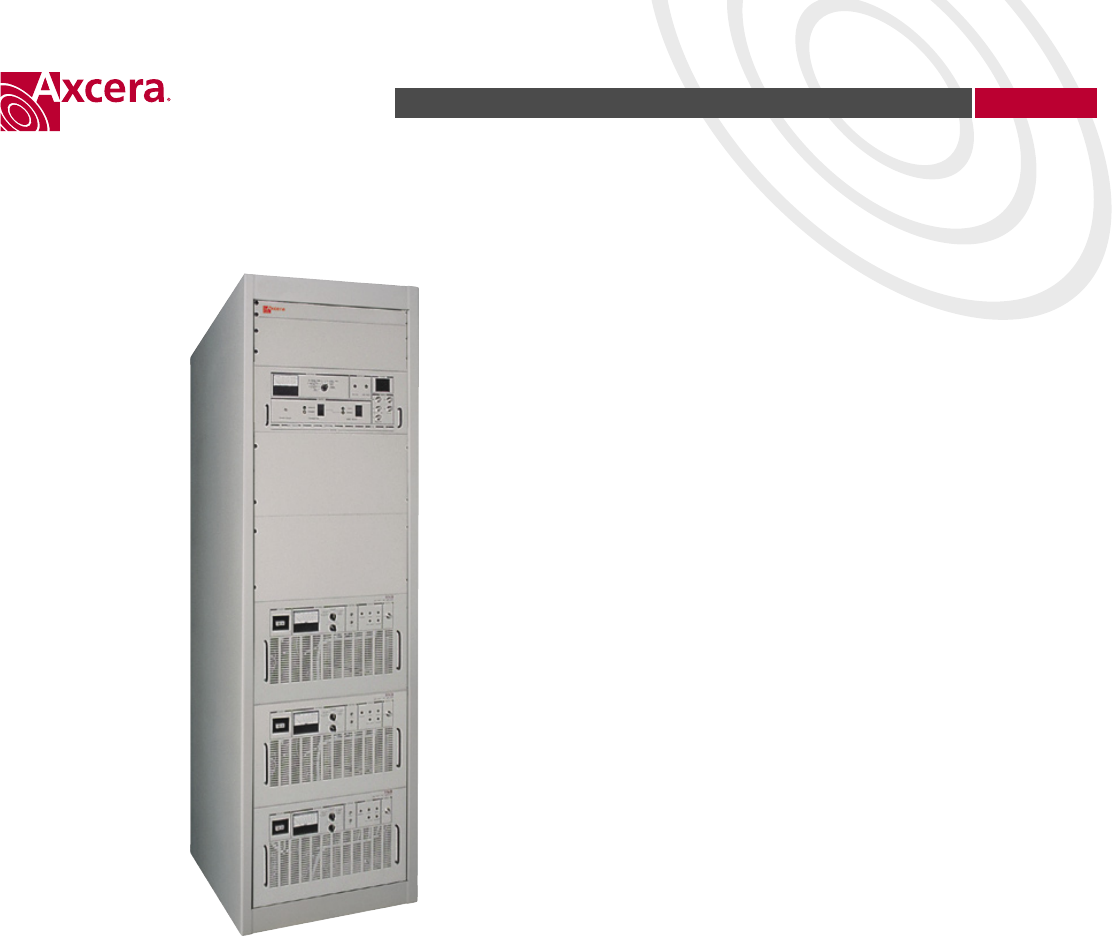
VHF Solid State Transmitter/Translator 300/400 Series
334B/336B 434B/436B
These low power VHF transmitters and translators deliver high quality and performance
in a compact and economical package. The time-proven Axcera exciter provides a
pre-corrected output directly to the high-gain nal power ampli er modules. The
entire package is housed in a single 19 inch rack-mount cabinet.
Designed for high reliability and unattended operation, each power ampli er
utilizes a parallel ampli er design with a high level of protection circuitry. Features
such as VSWR cutback, overdrive protection and over-temperature protection ensure
on-air reliability. Convenient system monitoring is achieved through front panel
samples, status indicators and metering, most of which are remote controllable.

Speci cations published here are current as of the date of publication of this document. Because we are continuously improving our products, Axcera reserves the right to change speci cations
without prior notice. At any time, you may verify product speci cations by contacting our of ce. Axcera views it’s patent portfolio as an important corporate asset and vigorously enforces its patents.
Products or features contained herein may be covered by one or more U.S. or foreign patents.
0406R0
© 2004 Axcera
All Rights Reserved
An Equal Opportunity Employer
A Platinum Equity Company
103 Freedom Drive, PO Box 525, Lawrence, PA 15055
t: 724-873-8100
f:724-873-8105
www.axcera.com
Visual Performance
Power Output
2000W
Output Impedance
50
Ω
Frequency Range
334B/336B
54 to 88 MHz
434B/436B
174 to 216 MHz
Carrier Stability
±250 Hz
(Transmitters or Translators with FCR)
Frequency Translation Stability
±1 kHz
(Translators)
Regulation of RF Output Power
3%
Output Variation (Over 1 Frame)
2%
Sideband Response
-1.25 MHz and below
-20 dB
-0.75 to -0.5 MHz
-+0.5, -2.0 db
-0.5 to +3.58 MHz
±0.5 dB
3.58 MHz to 4.18 MHz
=0.5, -1.0 dB
Freq Response vs. Brightness
±0.5 dB
Differential Gain
5%
Incidental Phase Modulation
±3°
Linearity
(Low Frequency)
5%
Differential Phase
±3°
Signal-to-Noise Ratio
55 dB
2t K-Factor
2%
Envelope Delay
Transmitters
Per FCC
Standard
Translators
±40 ns
Video Input
(Transmitters)
75
Ω
Harmonic Radiation
-60 dB
Intermodulation Products
-52 (red eld)
Spurious
-60 dBm
(>3 MHz from channel edge)
Noise Figure
(Translator)
4.5 dB (max)
With Input Preamp
Input Dynamic Range
-65 to -25 dBm
(Translators)
Aural Performance
Power Output
(Average)
200W
Distortion
0.5%
FM Noise
-60 dB
AM Noise
-55 dB
Aural to Visual Separation
4.5 MHz,
±100 Hz
Composite Audio Input
(Transmitters)
Input Level
1V peak,
nominal
Input Impedance
75 ohms,
unbalanced
Frequency Range
(±0.5 dB resp.)
30 Hz to
120 kHz
Monaural Audio Input
Input Level
0 to +10 dBm
Input Impedance
600 ohms,
balanced
Freq Range
(±0.5 dB resp.)
30 Hz to
15 kHz
Pre-emphasis
75µs
Subcarrier Input
(Transmitters)
Input Level
1V peak,
nominal
Input Impedance
75 ohms,
unbalanced
Freq Range
(±0.5 dB resp.)
20 kHz to
120 kHz
General
Operational Temperature Range
-30°C to +50°C,
derate 2°C per
1000 ft. AMSL
Operational Humidity Range
0% to 95%
(Non-condensing)
Altitude*
8,500 feet
Transmitter Dimensions
Size (H x W x D)
69”x22”x34”
Weight
500 lbs
Line Voltage
208 or 240 V ±10%,
1 phase 50/60Hz
Power Consumption
4000 W (50% APL)
Options
Automatic Station Identi er
Spare Parts Kit
Modulator Option
(Translators)
Remote Preampli er
(Translators)
UHF Frequency Correcting Receiver
(FCR Option,Translators)
VHF Solid State Transmitter/Translator 300/400 Series
334B/336B 434B/436B
APPENDIX B
SAMPLE LOG REPORT SHEET
AND TYPICAL READINGS

2000-Watt VHF Low Band Transmitter Appendix B, Sample Log Report Sheet
334B, Rev. 0 B-1
VHF Exciter (A4)
ALC (0 to 1 V) = ____________V % Aural Power (0 to 120) = __________%
% Exciter (0 to 120) = ______________% Video (0 to 1 V) = ________________IRE
% Reflected (0 to 120) = ____________% Audio (0 to 100 kHz) = ____________kHz
% Visual Power (0 to 120) = _________%
VHF Amplifier Trays
#1 (A6) #2 (A7)
AGC Voltage (0 to 10 V) = ___________V AGC Voltage (0 to 10 V) = ___________V
% Reflected Power (0 to 120) = _______% % Reflected Power (0 to 120) = _______%
% Output Power (0 to 120) = ________% % Output Power (0 to 120) = ________%
Power Supply Voltage (0 to 100 V) = ___V Power Supply Voltage (0 to 100 V) = ___V
Current (0 to 10A scale, readings are then
multiplied by 2) Current (0 to 10A scale, readings are then
multiplied by 2)
Current I1 = ___________A Current I1 = ___________A
Current I2 = ___________A Current I2 = ___________A
Current I3 = ___________A Current I3 = ___________A
Current ID = ___________A Current ID = ___________A

2000-Watt VHF Low Band Transmitter Appendix B, Typical Readings
334B, Rev. 0 B-3
VHF Low Band Exciter Tray (A4)
ALC = .8V
% Exciter = The level needed to attain 100% output power from the transmitter
(Typically between 80 & 100%).
% Reflected = < 10%
% Visual Power = 100 % (2000 Watts Peak of Sync)
% Aural Power = 100 % (200 Watts @ 10 dB A/V Ratio)
Video = 1 V at White w/.3V Sync Only, -40 IRE
Audio = ±25 kHz with Balanced Audio Input or ±75 kHz with Stereo Composite
Audio Input
VHF Amplifier Trays (A6, A7 & A11)
AGC Voltage = 1 to 3V
% Reflected Power = < 5%
% Output Power = 100%
Power Supply Voltage = 30V
Operating Currents Idling Currents
Current I1 = 12A-13A (Black Picture) 1.8A (No RF Applied)
Current I2 = 12A-13A (Black Picture) 1.8A (No RF Applied)
Current I3 = 12A-13A (Black Picture) 1.8A (No RF Applied)
Current ID = 3A (Black Picture) 3A (No RF Applied)
(The readings are from the 0 to 10A scale with the value then multiplied by 2)

2000-Watt VHF Low Band Transmitter Appendix B, Sample Log Report Sheet
334B, Rev. 0 B-2
VHF Amplifier Trays
#3 (A11)
AGC Voltage (0 to 10 V) = ___________V
% Reflected Power (0 to 120) = _______%
% Output Power (0 to 120) = ________%
Power Supply Voltage (0 to 100 V) = ___V
Current (0 to 10A scale, readings are then
multiplied by 2)
Current I1 = ___________A
Current I2 = ___________A
Current I3 = ___________A
Current ID = ___________A
Date __________________
Customer Name ______________________________ Call Letters ________________
Technician ___________________________________________
APPENDIX C
ASSEMBLY DRAWINGS AND PARTS LISTS

2000-Watt VHF Low Band Transmitter Appendix C, Assembly Drawings
334B, Rev. 0 C-1
334B System:
334B VHF Low Band Transmitter Typical Racking Plan............................1304405
334B VHF Low Band Transmitter Block Diagram....................................1304535
334B VHF Low Band Transmitter Interconnect .....................................1304391
334B VHF Low Band Transmitter Interconnect w/Gentner.......................1304518
VHF Low Band Exciter Tray, M/N, Sync Tip Clamp
Block Diagram................................................................................1070906
Interconnect.................................................................................1070908
VHF Low Band Amplifier Tray, CH. 5-6
Block Diagram................................................................................1304364
Interconnect.................................................................................1304365
APPENDIX D
SUBASSEMBLY DRAWINGS AND PARTS LISTS

2000-Watt VHF Low Band Transmitter Appendix D, Subassembly Drawings
334B, Rev. 0 D-1
Differential Gain Corrector Board
Schematic ..................................................................................1138-3107
AGC Control Board
Schematic ..................................................................................1142-3601
Channel Oscillator Board, Dual Oven
Schematic ..................................................................................1145-3201
VCXO Channel Oscillator Board, Dual Oven (Used with Precise Frequency)
Schematic ..................................................................................1145-3204
(Optional) IF Attenuator Board (Used with AM Identifier Kit)
Schematic ..................................................................................1150-3201
VHF Low Band Filter/Mixer Board
Schematic ..................................................................................1153-3101
x2 Multiplier Board, VHF Low Band
Schematic ..................................................................................1172-3111
IF Carrier Oven Oscillator Board, 45.75MHz
Schematic ..................................................................................1191-3404
Overdrive Protection Board
Schematic ..................................................................................1198-3601
Phase Shifter Board, VHF Low Band
Schematic ..................................................................................1198-3602
Low Band VHF Amplifier Board
Schematic ..................................................................................1198-3605
Filter/Amplifier Board
Schematic ..................................................................................1198-3606
3 Way Splitter Board (CH. 5-6)
Schematic ..................................................................................1198-3608
3-Way Combiner Board (CH. 5-6)
Schematic ..................................................................................1198-3626
Delay Equalizer Board
Schematic ..................................................................................1227-3204
IF Phase Corrector Board
Schematic ..................................................................................1227-3250
IF Carrier VCXO Board, NTSC (Used with Precise Frequency)
Schematic ..................................................................................1248-3131
Sync Tip Clamp/Modulator Board
Schematic ..................................................................................1265-3302
Aural IF Synthesizer Board, 4.5 MHz
Schematic ..................................................................................1265-3303

2000-Watt VHF Low Band Transmitter Appendix D, Subassembly Drawings
334B, Rev. 0 D-2
ALC Board
Schematic ..................................................................................1265-3305
(Optional) EEPROM FSK Identifier Board (Used with AM Identifier Kit)
Schematic ..................................................................................1265-3308
Visual/Aural Metering Board
Schematic ..................................................................................1265-3309
Transmitter Control Board
Schematic ..................................................................................1265-3311
+12V(4A)-12V(1A) Power Supply Board
Schematic ..................................................................................1265-3312
VHF Low Band Filter/Amplifier Board
Schematic .....................................................................................1064146
Current Metering Board, VHF Low Band
Schematic .....................................................................................1304366
P400-VHF-L-18 400W Pk. Sync VHF LB Pallet (1304348)
Delta RF Technology Data Sheet...................................................P400-VHF-L