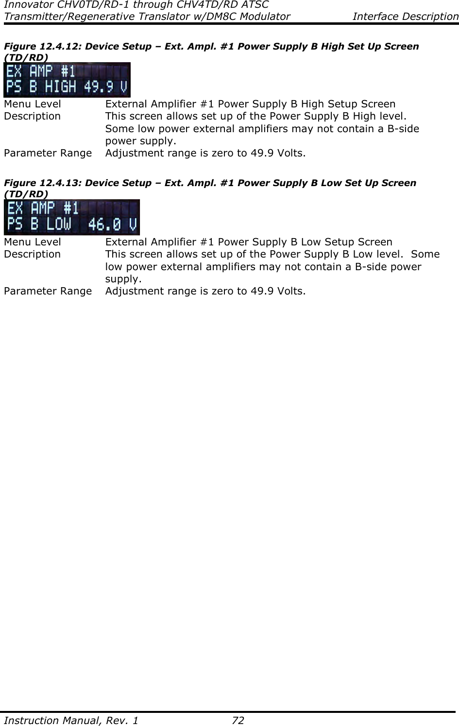
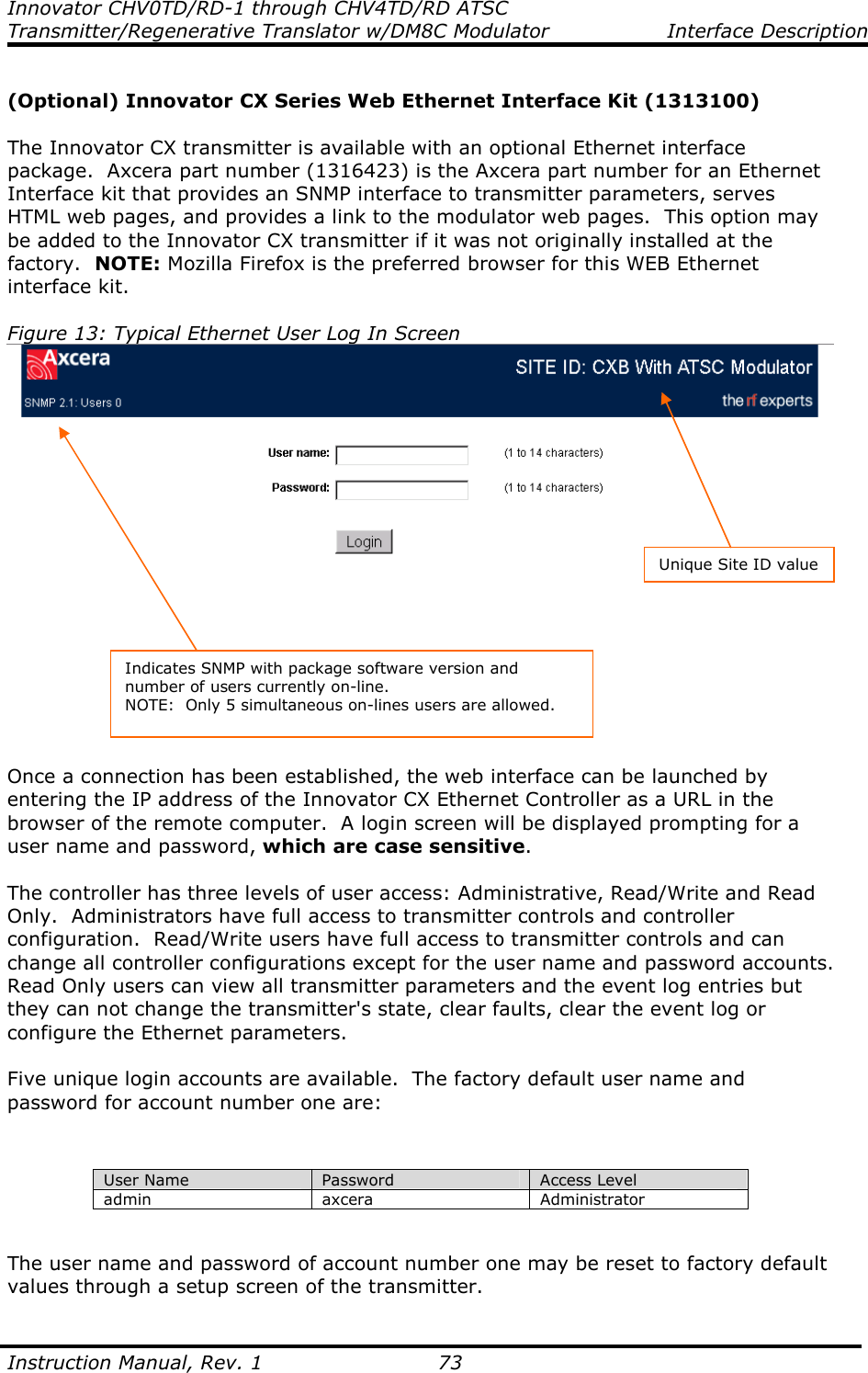
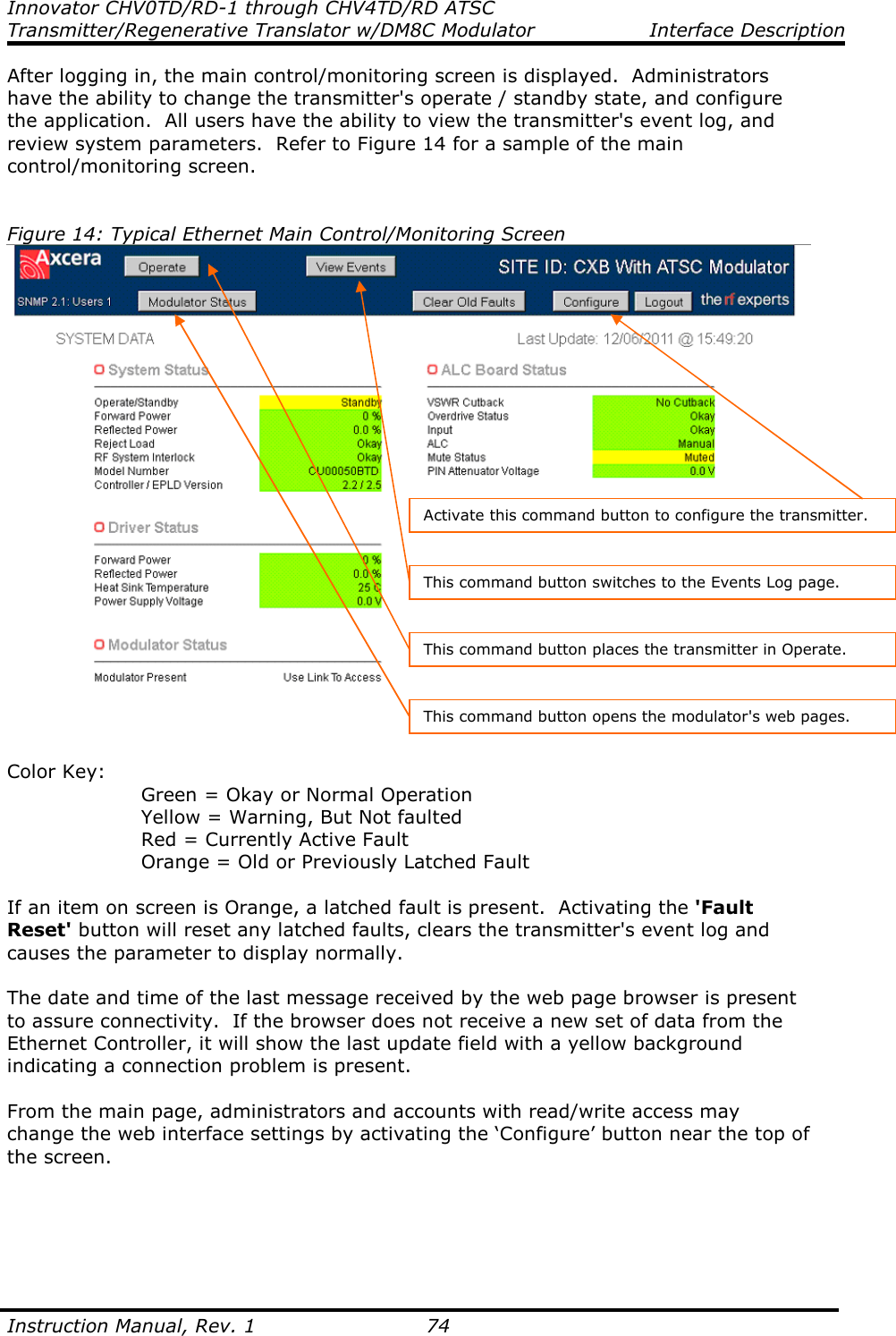
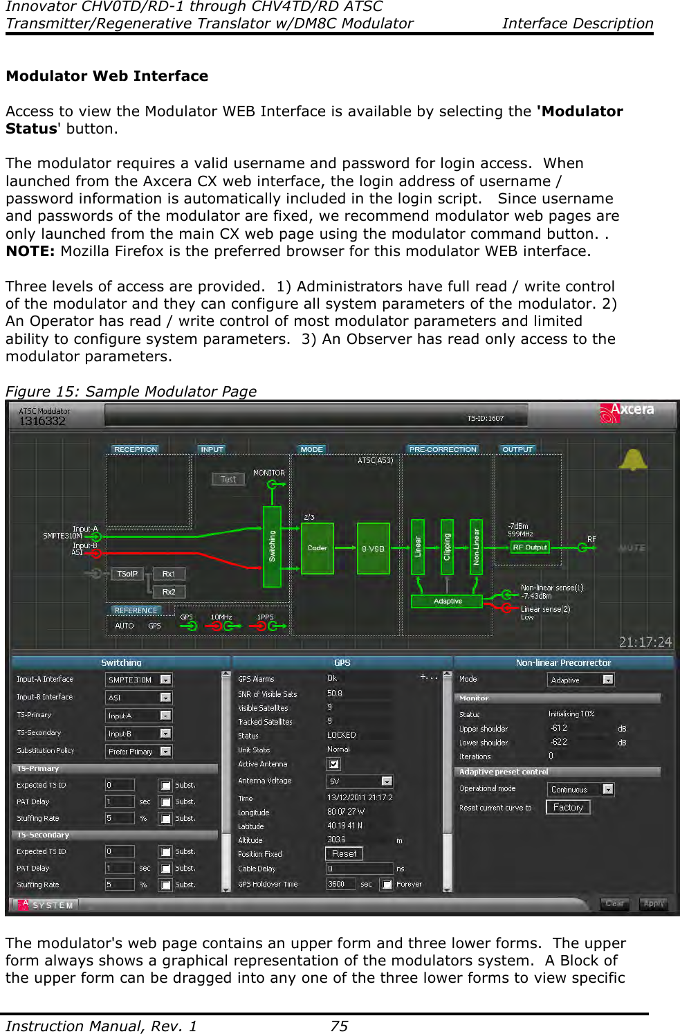
UBS Axcera CHV4TD 3000-Watt VHF Digital Transmitter User Manual
UBS-Axcera 3000-Watt VHF Digital Transmitter Users Manual
UserManual.wiki
>
UBS Axcera
>
CHV4TD User Manual
Users Manual
Navigation menu
Upload a User Manual
Namespaces
Wiki Guide
HTML
PDF
Info
Views
User Manual
Discussion / Help
Navigation
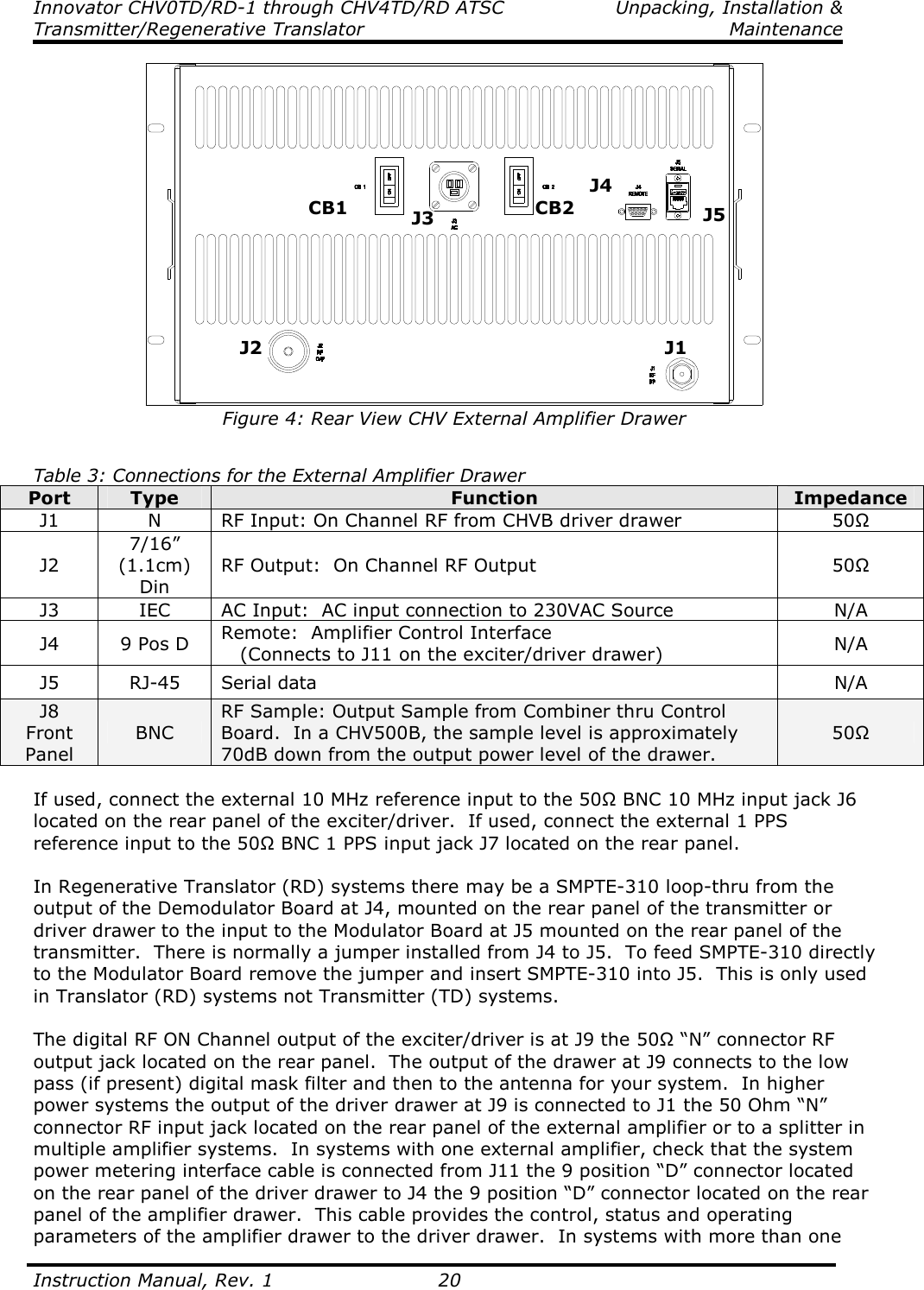
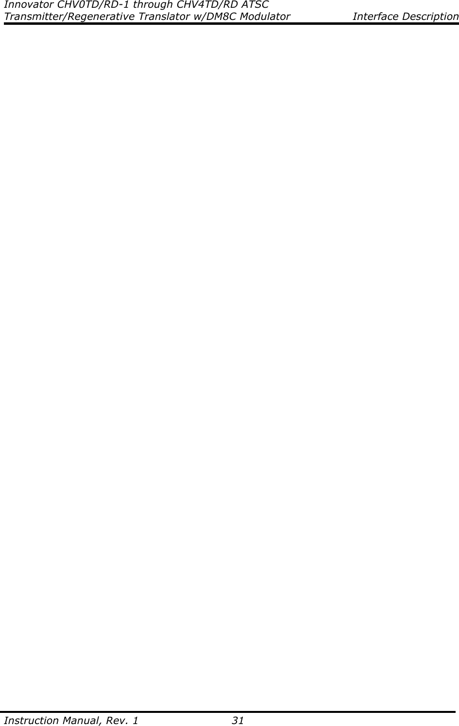
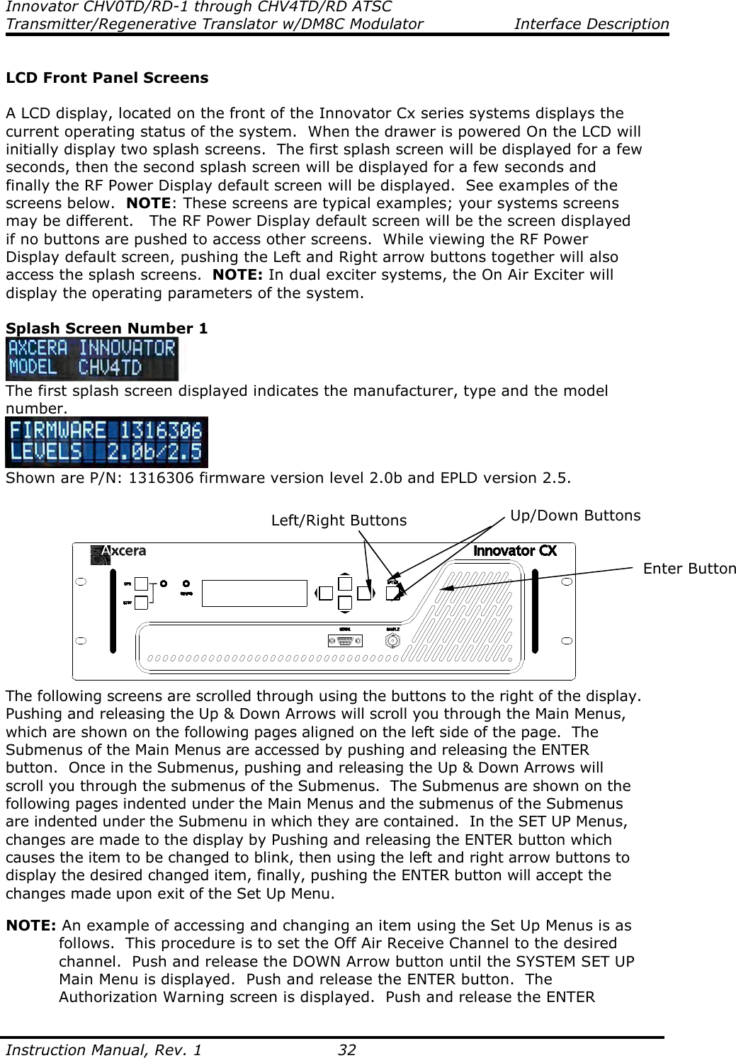
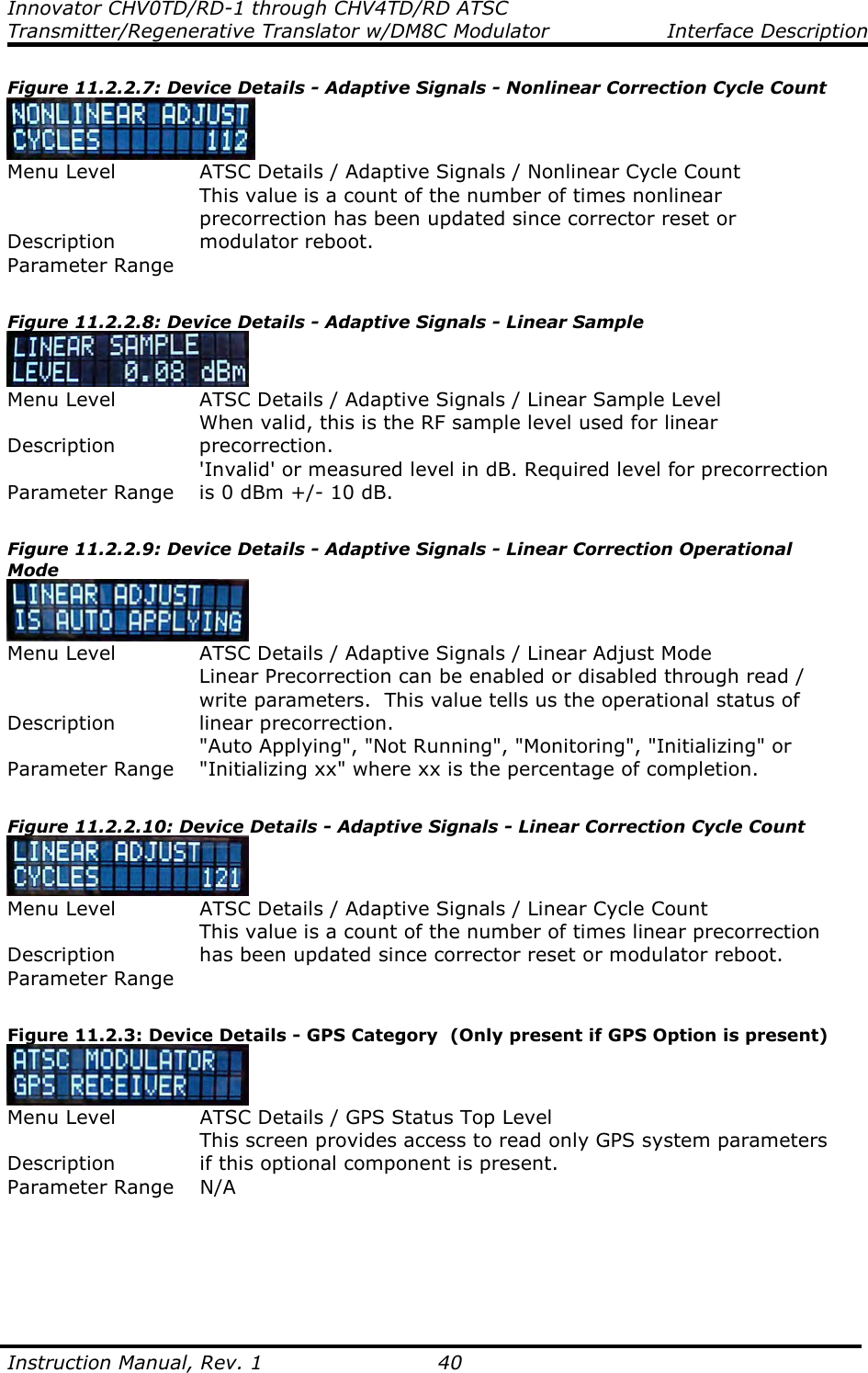
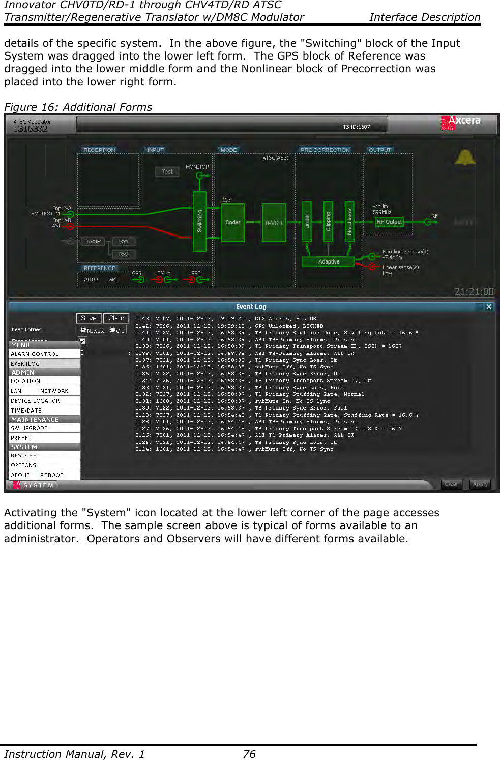
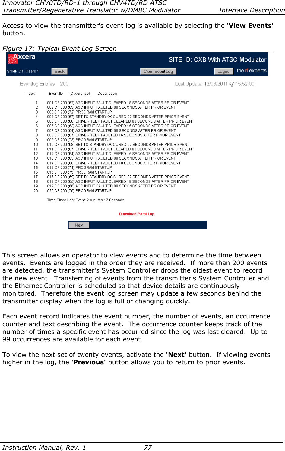
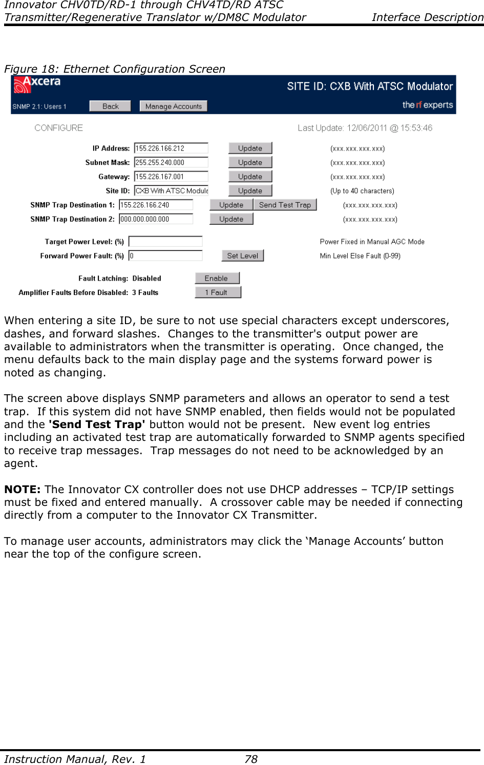
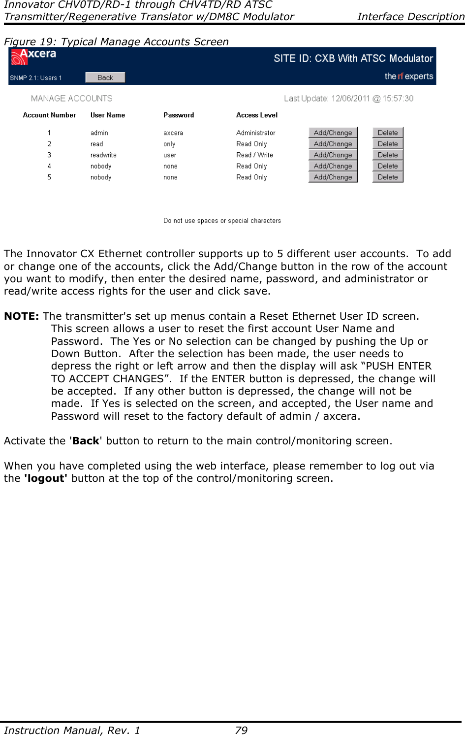
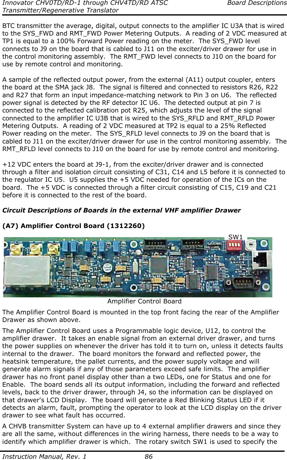
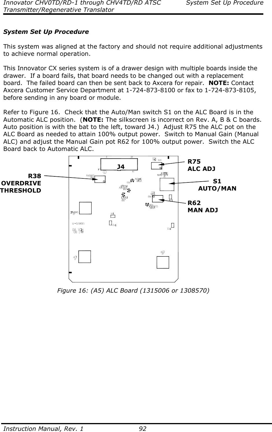
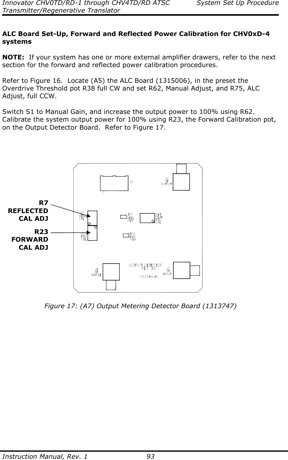
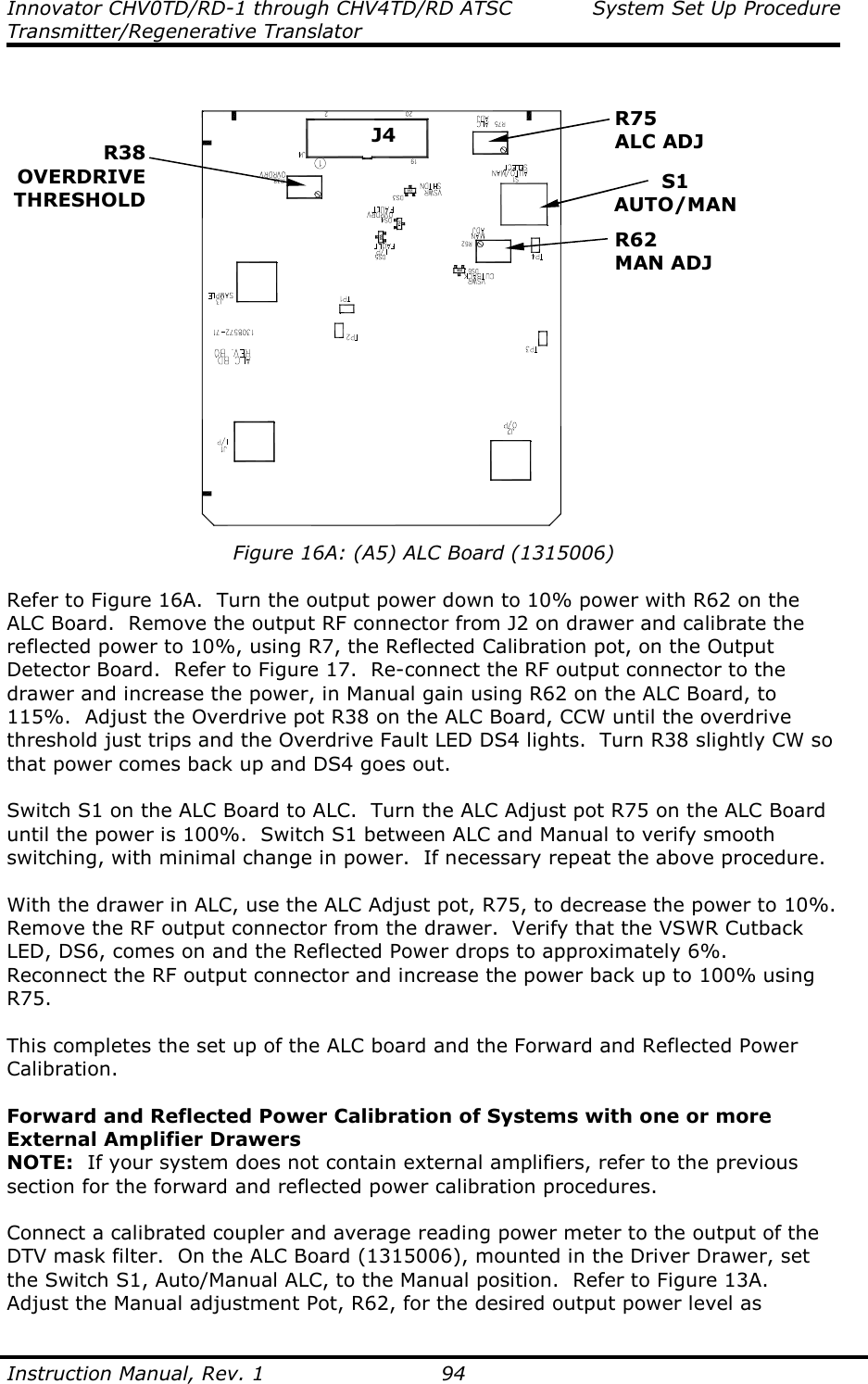
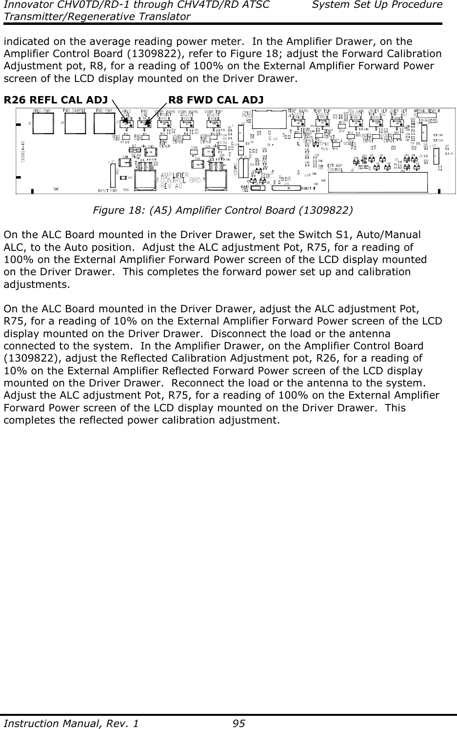
![Innovator CHV0TD/RD-1 through CHV4TD/RD ATSC Introduction Transmitter/Regenerative Translator Instruction Manual, Rev. 1 7 dBm, dBw, dBmV, dBµµµµV, & VOLTAGE EXPRESSED IN WATTS 50 Ohm System WATTS PREFIX dBm dBw dBmV dBµV VOLTAGE 1,000,000,000,000 1 TERAWATT +150 +120 100,000,000,000 100 GIGAWATTS +140 +110 10,000,000,000 10 GIGAWATTS +130 +100 1,000,000,000 1 GIGAWATT +120 + 99 100,000,000 100 MEGAWATTS +110 + 80 10,000,000 10 MEGAWATTS +100 + 70 1,000,000 1 MEGAWATT + 90 + 60 100,000 100 KILOWATTS + 80 + 50 10,000 10 KILOWATTS + 70 + 40 1,000 1 KILOWATT + 60 + 30 100 1 HECTROWATT + 50 + 20 50 + 47 + 17 20 + 43 + 13 10 1 DECAWATT + 40 + 10 1 1 WATT + 30 0 + 77 +137 7.07V 0.1 1 DECIWATT + 20 - 10 + 67 +127 2.24V 0.01 1 CENTIWATT + 10 - 20 + 57 +117 0.707V 0.001 1 MILLIWATT 0 - 30 + 47 +107 224mV 0.0001 100 MICROWATTS - 10 - 40 0.00001 10 MICROWATTS - 20 - 50 0.000001 1 MICROWATT - 30 - 60 0.0000001 100 NANOWATTS - 40 - 70 0.00000001 10 NANOWATTS - 50 - 80 0.000000001 1 NANOWATT - 60 - 90 0.0000000001 100 PICOWATTS - 70 -100 0.00000000001 10 PICOWATTS - 80 -110 0.000000000001 1 PICOWATT - 90 -120 TEMPERATURE CONVERSION °°°°F = 32 + [(9/5) °°°°C] °°°°C = [(5/9) (°°°°F - 32)]](https://usermanual.wiki/UBS-Axcera/CHV4TD/User-Guide-1724136-Page-11.png)