UBS Axcera CHV4TD 3000-Watt VHF Digital Transmitter User Manual
UBS-Axcera 3000-Watt VHF Digital Transmitter Users Manual
Users Manual

Instruction Manual
Innovator,
CHV0TD-1/RD-1 thru
CHV4TD/RD,
ATSC VHF High Band Transmitter/
Regenerative Translator
Axcera, LLC
103 Freedom Drive • P.O. Box 525 • Lawrence, PA 15055-0525, USA
Phone: 724-873-8100 • Fax: 724-873-8105
www.axcera.com • info@axcera.com
RESTRICTIONS ON USE, DUPLICATION OR DISCLOSURE
OF PROPRIETARY INFORMATION
This document contains information proprietary to Axcera, to its affiliates or to a third party to
which Axcera may have a legal obligation to protect such information from unauthorized
disclosure, use or duplication. Any disclosure, use or duplication of this document or any of the
information herein for other than the specific purpose for which it was disclosed by Axcera is
expressly prohibited, except as Axcera may otherwise agree in writing. Recipient by accepting this
document agrees to the above stated conditional use of this document and this information
disclosed herein.
Copyright © 2011, Axcera

Innovator CHV0TD/RD-1 through CHV4TD/RD ATSC Table of Contents
Transmitter/Regenerative Translator
Instruction Manual, Rev. 1 i 4/11/11
Table of Contents
Introduction ......................................................................................................1
Manual Overview ............................................................................................1
Assembly Designators .....................................................................................1
Safety ...........................................................................................................1
Contact Information........................................................................................3
Return Material Procedure ...............................................................................3
Limited One Year Warranty for Axcera Products..................................................4
System Description ..........................................................................................11
Unpacking, Installation and Maintenance ............................................................14
Unpacking ...................................................................................................14
Installation ..................................................................................................14
Drawer Slide Installation ............................................................................15
AC Input Connections .......................................................................................16
Input and Output Connections ...........................................................................17
J11 Power Monitoring Connections .....................................................................19
Maintenance ................................................................................................21
Initial On Site Turn On Procedure.......................................................................24
Typical System Operating Parameters ................................................................25
Typical Problems, Indications and Causes in Exciter/Driver Drawer ........................27
LCD Display and Front Panel LED Indicators ........................................................27
System Remote Connections to J12....................................................................29
LCD Front Panel Screens ...............................................................................32
Operation Screens ........................................................................................33
Device Details Screens - These are read only parameters. ....................................35
Device Setup Screens - These are read / write parameters. .................................. 47
(Optional) Innovator CX Series Web Ethernet Interface Kit (1313100)....................73
Modulator Web Interface...................................................................................75
SNMP Interfaces ..............................................................................................80
Circuit Descriptions of Boards in the CHV0xD-1 & CHV0xD-4 System.....................81
(A1) 8 VSB Demodulator Board (1308275) - Only used with RD operation ...........81
Overview..................................................................................................81
Microcontroller Functions............................................................................ 81
Jumper and DIP Switch Settings..................................................................81
(A2) Digital Modulator Board DM8C (1316332) ............................................. 82
(A5) ALC Board, Innovator CX Series (1315006) ..............................................82
(A6) Amplifier Assembly (1313959) – Used in the CHV0xD-1 Drawer ..................83
(A6-A1) VHF HB Pre-Driver Assembly (1313899) ..........................................83
(A6-A2) 50 Watt Amplifier Pallet, Italmec (1313484) .....................................83
(A6) 200 Watt Driver Amplifier Assembly (1315010 used w/Axciter Drawer or
1313912 used in all other applications) – Used in the CHVxD-4 ..........................83
(A6-A1) 50 Watt Amplifier Pallet, Italmec (1313484) .....................................83
(A6-A2) 500 Watt Amplifier Pallet, Italmec (1313581) ...................................84
(A7) Output Metering Detector Board (1313747) ..............................................84
(A8) Control Card, Innovator CX (1312543) .....................................................84
(A9 & A10) Power Supplies used in CHV0xD-1 and CHV0xD-4 ............................85
Circuit Description of External System Metering Board which is only used in
Transmitters with multiple external Amplifier Drawers ..........................................85
(A5) System Metering Board (1312666) ..........................................................85
Circuit Descriptions of Boards in the external VHF amplifier Drawer........................86
(A7) Amplifier Control Board (1312260) ..........................................................86
(A10) Current Metering Board (1309130) ........................................................87
(A5) 2 Way VHF Splitter Board (1313941) .......................................................87

Innovator CHV0TD/RD-1 through CHV4TD/RD ATSC Table of Contents
Transmitter/Regenerative Translator
Instruction Manual, Rev. 1 ii 4/11/11
(A2 & A3) 500 Watt LDMOS Amplifier Pallets (1313581)....................................87
(A6) 2 Way VHF Combiner Board (1313969) ....................................................87
(A8 & A9) VHF Amplifier Drawer Power Supplies...............................................88
Circuit Descriptions of Boards in the CHV500B/600B, 500/600 Watt ATSC Amplifier
Drawer ...........................................................................................................88
(A7) Amplifier Control Board (1312260) ..........................................................88
(A10) Current Metering Board (1309130) ........................................................89
(A5) 4 Way Splitter Board (1313938)..............................................................89
(A1, A2, A3 & A4) 500 Watt LDMOS Amplifier Pallets (1313581) ........................89
(A6) 4 Way Combiner Board (1313965) ..........................................................90
(A8 & A9) CHV500B/600B, Two 48 VDC/2250 Watt Power Supplies ....................90
System Set Up Procedure .................................................................................92
ALC Board Set-Up, Forward and Reflected Power Calibration for CHV0xD-4 systems
..................................................................................................................93
Forward and Reflected Power Calibration of Systems with one or more External
Amplifier Drawers ......................................................................................... 94
APPENDIX A: ........................................................................................................1
Innovator CHV0xD VHF High Band
Regenerative Translator System and Drawer
Drawing List .........................................................................................................1
Innovator CHV0TD/RD-1 through CHV4TD/RD ATSC Introduction
Transmitter/Regenerative Translator
Instruction Manual, Rev. 1 1
Introduction
Manual Overview
This manual contains the description of the Innovator CHV0TD-1/RD-1 thru CHV4TD/RD
ATSC Transmitter or Regenerative Translator and the circuit descriptions of the boards,
which make up the system. The manual also describes the installation, setup and
alignment procedures for the system. Appendix A of this manual contains the system
drawings and parts lists for the Innovator Transmitter or Regenerative Translator
System. NOTES: 1) Information and drawings on the Axciter Digital Modulator, if part
of your system, are contained in the separate Axciter Instruction Manual. 2)
Information and drawings on the K-Tech receiver, if part of your system, are contained
in the separate K-Tech Instruction Manual. 3) If your system contains dual exciters with
a remote interface panel and Exciter control panel, information and drawings on the
system and panels are contained in the separate remote interface panel instruction
manual.
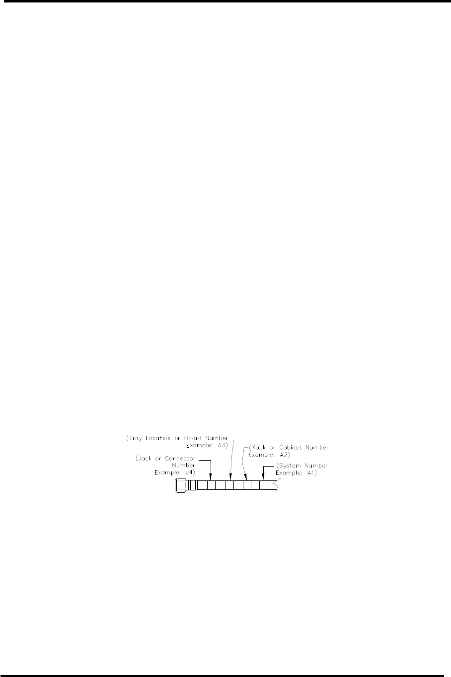
Assembly Designators
Axcera has assigned assembly numbers, Ax designations such as A1, where x=1,2,3…etc,
to all assemblies, modules, and boards in the system. These designations are referenced
in the text of this manual and shown on the block diagram and interconnect drawings
provided in Appendix A.
The cables that connect between the boards within a drawer or assembly and that
connect between the drawers, racks and cabinets are labeled using markers. Figure 1 is
an example of a marked cable. There may be as few as two or as many as four Markers
on any one cable. These markers are read starting farthest from the connector. If there
are four Markers, the marker farthest from the connector is the system number such as
system 1 or transmitter 2. The next or the farthest Marker is the rack or cabinet “A”
number on an interconnect cable or the board “A” number when the cable is within a
drawer. The next number on an interconnect cable is the Drawer location or Board “A”
number. The marker closest to the connector is the jack or connector “J” number on an
interconnect cable or the jack or connector “J” number on the board when the cable is
within a drawer.
4 3 2 1
Marker Identification Drawing
Safety
The Innovator CX Transmitter or Regenerative Translator Systems manufactured by
Axcera are designed to be easy to use and repair while providing protection from electrical
and mechanical hazards. Please review the following warnings and familiarize yourself
with the operation and servicing procedures before working on the system.
Hazardous Accessibility – Axcera has made attempts to provide appropriate
connectors, wiring and shields to minimize hazardous accessibility.
Circuit Breakers and Wiring – All circuit breakers and wire are UL and CE certified and
are rated for maximum operating conditions.

Innovator CHV0TD/RD-1 through CHV4TD/RD ATSC Introduction
Transmitter/Regenerative Translator
Instruction Manual, Rev. 1 2
Single Point Breaker or Disconnect - The customer should provide a single point
breaker or disconnect at the breaker box for the main AC input connection to the
transmitter.
Transmitter Ratings - The transmitter ratings are provided in the text of this manual
along with voltage and current values for the equipment.
Protective Earthing Terminal – A main protective earthing terminal is provided for
equipment required to have protective earthing.
Read All safety Instructions – All of the safety instructions should be read and
understood before operating this equipment.
Retain Manuals – The manuals for the system should be retained at the system site for
future reference. Axcera provides two manuals for this purpose; one manual can be left
at the office while the other can be kept at the site.
Heed all Notes, Warnings, and Cautions – All of the notes, warnings, and cautions
listed in this safety section and throughout the manual must be followed.
Follow Operating Instructions – All of the operating and use instructions for the
system should be followed.
Cleaning – Unplug or otherwise disconnect all power from the equipment before cleaning.
Do not use liquid or aerosol cleaners. Use only a damp cloth for cleaning.
Ventilation – Openings in the cabinet and module front panels are provided for
ventilation. To ensure the reliable operation of the system, and to protect the unit from
overheating, these openings must not be blocked.
Servicing – Do not attempt to service this product yourself until becoming familiar with
the equipment. If in doubt, refer all servicing questions to qualified Axcera service
personnel.
Replacement Parts – When replacement parts are used, be sure that the parts have the
same functional and performance characteristics as the original part. Unauthorized
substitutions may result in fire, electric shock, or other hazards. Please contact the
Axcera Technical Service Department if you have any questions regarding service or
replacement parts.

Innovator CHV0TD/RD-1 through CHV4TD/RD ATSC Introduction
Transmitter/Regenerative Translator
Instruction Manual, Rev. 1 3
Contact Information
The Axcera Field Service Department can be contacted by PHONE at 724-873-8100 or by
FAX at 724-873-8105.
Before calling Axcera, please be prepared to supply the Axcera technician with answers to
the following questions. This will save time and help ensure the most direct resolution to
the problem.
1. What are your Name and the Call Letters for the station?
2. What are the model number and type of system?
3. Is the system digital or analog?
4. How long has the system been on the air? (Approximately when was the system
installed?)
5. What are the symptoms being exhibited by the system? Include the current front
panel LCD readings and what the status LED is indicating on the front panel of
the drawer. If possible, include the LCD readings before the problem occurred.
Return Material Procedure
To insure the efficient handling of equipment or components that have been returned for
repair, Axcera requests that each returned item be accompanied by a Return Material
Authorization Number (RMA#). The RMA# can be obtained from any Axcera Field
Service Engineer by contacting the Axcera Field Service Department at 724-873-8100 or
by Fax at 724-873-8105. This procedure applies to all items sent to the Field Service
Department regardless of whether the item was originally manufactured by Axcera.
When equipment is sent to the field on loan, the RMA# is included with the unit. The RMA#
is intended to be used when the unit is returned to Axcera. In addition, all shipping
material should be retained for the return of the unit to Axcera.
Replacement assemblies are also sent with the RMA# to allow for the proper routing of the
exchanged hardware. Failure to close out this type of RMA# will normally result in the
customer being invoiced for the value of the loaner item or the exchanged assembly.
When shipping an item to Axcera, please include the RMA# on the packing list and on the
shipping container. The packing slip should also include contact information and a brief
description of why the unit is being returned.
Please forward all RMA items to:
AXCERA, LLC
103 Freedom Drive
P.O. Box 525
Lawrence, PA 15055-0525 USA
For more information concerning this procedure, call the Axcera Field Service Department
at 724-873-8100.
Axcera can also be contacted through e-mail at info@axcera.com and on the Web at
www.axcera.com.

Innovator CHV0TD/RD-1 through CHV4TD/RD ATSC Introduction
Transmitter/Regenerative Translator
Instruction Manual, Rev. 1 4
Limited One Year Warranty for Axcera Products
Axcera warrants each new product that it has manufactured and sold against defects in
material and workmanship under normal use and service for a period of one (1) year
from the date of shipment from Axcera's plant, when operated in accordance with
Axcera's operating instructions. This warranty shall not apply to tubes, fuses, batteries,
bulbs or LEDs.
Warranties are valid only when and if (a) Axcera receives prompt written notice of
breach within the period of warranty, (b) the defective product is properly packed and
returned by the buyer (transportation and insurance prepaid), and (c) Axcera
determines, in its sole judgment, that the product is defective and not subject to any
misuse, neglect, improper installation, negligence, accident, or (unless authorized in
writing by Axcera) repair or alteration. Axcera's exclusive liability for any personal
and/or property damage (including direct, consequential, or incidental) caused by the
breach of any or all warranties, shall be limited to the following: (a) repairing or
replacing (in Axcera's sole discretion) any defective parts free of charge (F.O.B. Axcera’s
plant) and/or (b) crediting (in Axcera's sole discretion) all or a portion of the purchase
price to the buyer.
Equipment furnished by Axcera, but not bearing its trade name, shall bear no warranties
other than the special hours-of-use or other warranties extended by or enforceable
against the manufacturer at the time of delivery to the buyer.
NO WARRANTIES, WHETHER STATUTORY, EXPRESSED, OR IMPLIED, AND NO
WARRANTIES OF MERCHANTABILITY, FITNESS FOR ANY PARTICULAR
PURPOSE, OR FREEDOM FROM INFRINGEMENT, OR THE LIKE, OTHER THAN AS
SPECIFIED IN PATENT LIABILITY ARTICLES, AND IN THIS ARTICLE, SHALL
APPLY TO THE EQUIPMENT FURNISHED HEREUNDER.

Innovator CHV0TD/RD-1 through CHV4TD/RD ATSC Introduction
Transmitter/Regenerative Translator
Instruction Manual, Rev. 1 5
WARNING!!!
HIGH VOLTAGE
DO NOT ATTEMPT TO REPAIR OR TROUBLESHOOT THIS EQUIPMENT UNLESS
YOU ARE FAMILIAR WITH ITS OPERATION AND EXPERIENCED IN
SERVICING HIGH VOLTAGE EQUIPMENT. LETHAL VOLTAGES ARE PRESENT
WHEN POWER IS APPLIED TO THIS SYSTEM. IF POSSIBLE, TURN OFF
POWER BEFORE MAKING ADJUSTMENTS TO THE SYSTEM.
RADIO FREQUENCY RADIATION HAZARD
MICROWAVE, RF AMPLIFIERS AND TUBES GENERATE HAZARDOUS RF
RADIATION THAT CAN CAUSE SEVERE INJURY INCLUDING CATARACTS,
WHICH CAN RESULT IN BLINDNESS. SOME CARDIAC PACEMAKERS MAY BE
AFFECTED BY THE RF ENERGY EMITTED BY RF AND MICROWAVE
AMPLIFIERS. NEVER OPERATE THE TRANSMITTER SYSTEM WITHOUT A
PROPERLY MATCHED RF ENERGY ABSORBING LOAD OR THE ANTENNA
ATTACHED. KEEP PERSONNEL AWAY FROM OPEN WAVEGUIDES AND
ANTENNAS. NEVER LOOK INTO AN OPEN WAVEGUIDE OR ANTENNA.
MONITOR ALL PARTS OF THE RF SYSTEM FOR RADIATION LEAKAGE AT
REGULAR INTERVALS.

Innovator CHV0TD/RD-1 through CHV4TD/RD ATSC Introduction
Transmitter/Regenerative Translator
Instruction Manual, Rev. 1 6
EMERGENCY FIRST AID INSTRUCTIONS
Personnel engaged in the installation, operation, or maintenance of this equipment are
urged to become familiar with the following rules both in theory and practice. It is the
duty of all operating personnel to be prepared to give adequate Emergency First Aid and
thereby prevent avoidable loss of life.
RESCUE BREATHING
1. Find out if the person is
breathing.
You must find out if the
person has stopped breathing.
If you think he is not
breathing, place him flat on
his back. Put your ear close to
his mouth and look at his
chest. If he is breathing you
can feel the air on your
cheek. You can see his chest
move up and down. If you do
not feel the air or see the
chest move, he is not
breathing.
2. If he is not breathing,
open the airway by tilting his
head backwards.
Lift up his neck with one
hand and push down on his
forehead with the other. This
opens the airway. Sometimes
doing this will let the person
breathe again by himself.
3. If he is still not breathing,
begin rescue breathing.
-Keep his head tilted
backward. Pinch nose shut.
-Put your mouth tightly over
his mouth.
-Blow into his mouth once
every five seconds
-DO NOT STOP rescue
breathing until help arrives.
LOOSEN CLOTHING - KEEP
WARM
Do this when the victim is
breathing by himself or help
is available. Keep him as
quiet as possible and from
becoming chilled. Otherwise
treat him for shock.
BURNS
SKIN REDDENED: Apply ice cold water to
burned area to prevent burn from going
deeper into skin tissue. Cover area with a
clean sheet or cloth to keep away air. Consult
a physician.
SKIN BLISTERED OR FLESH CHARRED:
Apply ice cold water to burned area to
prevent burn from going deeper into skin
tissue.
Cover area with clean sheet or cloth to keep
away air. Treat victim for shock and take to
hospital.
EXTENSIVE BURN - SKIN BROKEN: Cover
area with clean sheet or cloth to keep away
air. Treat victim for shock and take to
hospital.
Innovator CHV0TD/RD-1 through CHV4TD/RD ATSC Introduction
Transmitter/Regenerative Translator
Instruction Manual, Rev. 1 7
dBm, dBw, dBmV, dBµ
µµ
µV, & VOLTAGE
EXPRESSED IN WATTS
50 Ohm System
WATTS PREFIX dBm dBw dBmV dBµV VOLTAGE
1,000,000,000,000 1 TERAWATT +150
+120
100,000,000,000 100 GIGAWATTS +140
+110
10,000,000,000 10 GIGAWATTS +130
+100
1,000,000,000 1 GIGAWATT +120
+ 99
100,000,000 100 MEGAWATTS +110
+ 80
10,000,000 10 MEGAWATTS +100
+ 70
1,000,000
1 MEGAWATT + 90 + 60
100,000
100 KILOWATTS + 80 + 50
10,000 10 KILOWATTS + 70 + 40
1,000 1 KILOWATT + 60 + 30
100 1 HECTROWATT + 50 + 20
50
+ 47 + 17
20
+ 43 + 13
10
1 DECAWATT + 40 + 10
1
1 WATT + 30 0 + 77 +137 7.07V
0.1
1 DECIWATT + 20 - 10 + 67 +127 2.24V
0.01 1 CENTIWATT + 10 - 20 + 57 +117 0.707V
0.001 1 MILLIWATT 0 - 30 + 47 +107 224mV
0.0001 100 MICROWATTS - 10 - 40
0.00001
10 MICROWATTS - 20 - 50
0.000001
1 MICROWATT - 30 - 60
0.0000001 100 NANOWATTS - 40 - 70
0.00000001 10 NANOWATTS - 50 - 80
0.000000001 1 NANOWATT - 60 - 90
0.0000000001 100 PICOWATTS - 70 -100
0.00000000001 10 PICOWATTS - 80 -110
0.000000000001 1 PICOWATT - 90 -120
TEMPERATURE CONVERSION
°
°°
°F = 32 + [(9/5) °
°°
°C]
°
°°
°C = [(5/9) (°
°°
°F - 32)]

Innovator CHV0TD/RD-1 through CHV4TD/RD ATSC Introduction
Transmitter/Regenerative Translator
Instruction Manual, Rev. 1 8
USEFUL CONVERSION FACTORS
TO CONVERT FROM TO MULTIPLY BY
mile (US statute) kilometer (km) 1.609347
inch (in) millimeter (mm) 25.4
inch (in) centimeter (cm) 2.54
inch (in) meter (m) 0.0254
foot (ft) meter (m) 0.3048
yard (yd) meter (m) 0.9144
mile per hour (mph) kilometer per hour(km/hr) 1.60934
mile per hour (mph) meter per second (m/s) 0.44704
pound (lb) kilogram (kg) 0.4535924
gallon (gal) liter 3.7854118
U.S. liquid
(One U.S. gallon equals 0.8327 Canadian gallon)
fluid ounce (fl oz) milliliters (ml) 29.57353
British Thermal Unit watt (W) 0.2930711
per hour (Btu/hr)
horsepower (hp) watt (W) 746
NOMENCLATURE OF FREQUENCY BANDS
FREQUENCY RANGE DESIGNATION
3 to 30 kHz VLF - Very Low Frequency
30 to 300 kHz LF - Low Frequency
300 to 3000 kHz MF - Medium Frequency
3 to 30 MHz HF - High Frequency
30 to 300 MHz VHF - Very High Frequency
300 to 3000 MHz UHF - Ultrahigh Frequency
3 to 30 GHz SHF - Superhigh Frequency
30 to 300 GHz EHF - Extremely High Frequency
LETTER DESIGNATIONS FOR UPPER FREQUENCY BANDS
LETTER FREQ. BAND
L 1000 - 2000 MHz
S 2000 - 4000 MHz
C 4000 - 8000 MHz
X 8000 - 12000 MHz
Ku 12 - 18 GHz
K 18 - 27 GHz
Ka 27 - 40 GHz
V 40 - 75 GHz
W 75 - 110 GHz

Innovator CHV0TD/RD-1 through CHV4TD/RD ATSC Introduction
Transmitter/Regenerative Translator
Instruction Manual, Rev. 1 9
RETURN LOSS VS. VSWR
1.001 1.01 1.1 2.0
VSWR
0
-
10
-
20
-
30
-
40
-
50
-
60
-
70
R
E
T
U
R
N
L
O
S
S
dB

Innovator CHV0TD/RD-1 through CHV4TD/RD ATSC Introduction
Transmitter/Regenerative Translator
Instruction Manual, Rev. 1 10
ABBREVIATIONS/ACRONYMS
AC Alternating Current
AFC Automatic Frequency
Control
ALC Automatic Level Control
AM Amplitude Modulation
AGC Automatic Gain Control
ARD A-line, Regenerative
Translator, Digital
ATD A-line, Transmitter,
Digital
ATSC Advanced Television
Systems Committee (Digital)
AWG American Wire Gauge
BER Bit Error Rate
BRD B-line, Regenerative
Translator, Digital
BTD B-line, Transmitter,
Digital
BW Bandwidth
COFDM Coded Orthogonal Frequency
Division Multiplexing
modulation scheme
DC Direct Current
D/A Digital to Analog
DSP Digital Signal Processing
DTV Digital Television
dB Decibel
dBm Decibel referenced to
1 milliwatt
dBmV Decibel referenced to
1 millivolt
dBw Decibel referenced to 1 watt
FEC Forward Error Correction
FM Frequency Modulation
FPGA Field Programmable Gate
Array
Hz Hertz
ICPM Incidental Carrier Phase
Modulation
I/P Input
IF Intermediate Frequency
LED Light emitting diode
LSB Lower Sideband
LDMOS Lateral Diffused Metal Oxide
Semiconductor Field Effect
Transistor
MPEG Motion Pictures Expert
Group
NTSC National Television
Systems Committee (Analog)
O/P Output
PLL Phase Locked Loop
PCB Printed Circuit Board
QAM Quadrature Amplitude
Modulation
SMPTE Society of Motion Picture
and Television Engineers
VSB Vestigial Side Band

Innovator CHV0TD/RD-1 through CHV4TD/RD ATSC System Description
Transmitter/Regenerative Translator
Instruction Manual, Rev. 1 11
System Description
The Innovator CHV transmitter systems are of two different types. They are
either Regenerative Translators example: CHV0RD-4, or DTV Transmitters
example: CHV0TD-4. The Regenerative Translator (RD) accepts an RF On
Channel signal (-75 to –8 dBm) and converts it to a DTV RF On Channel output
signal. The DTV System (TD) takes a SMPTE-310 or DVB-ASI input and converts
it to a DTV RF On Channel output signal. The output power of either
configuration is typically up to 200 Watts ATSC using a single drawer. For
powers above 850W additional amplifiers may be paralleled. Typical
configurations; 1600 Watts ATSC with two Amplifier drawers, 2000 Watts ATSC
with three Amplifier drawers, 3000 Watts ATSC with four Amplifier drawers, 4000
Watts ATSC with six Amplifier drawers, and 6000 Watts ATSC with eight Amplifier
drawers. The Innovator CHV transmitter system provides linear and nonlinear
correction capability for the transmission path as well as internal test sources
that are used during initial system installation.
The CHV0xD-1 and CHV0xD-4 are used as the driver drawer for higher power
systems and contain the DM8C Digital Modulator (1316332). Systems with an
external Axciter Modulator Drawer the DM8C Digital Modulator and is replaced by
the (A3) Down-converter Board (131103). The amplifier assembly (A6), (A7)
Output Metering Detector Board (1313747), (A8) the Innovator CX Control Board
(1312543), (A9) the +5V, ±12V Power Supply and (A10) the +28V/+42VDC
Power Supply are also contained in the drawer. The RD kit (1310182) supplies
the (A1) 8 VSB Demodulator Board (1308275) to the drawer to make it a
regenerative translator.
The type of (A6) Amplifier assembly used in the drawer changes as the output
power of the system changes. The Amplifier Assembly (1315013 or 1313959) is
used in CHV0xD-1 systems and the Amplifier Assembly (1315010 or 1313912) is
used in CHV0xD-4 systems.
The (A10) Power Supply Assembly also changes as the output power of the
system changes. A +48V/300W Power Supply is used in CHV0xD-1 systems and
a +48V/1100W Power Supply is used in CHV0xD-4 systems.
When configured as an ATSC Transmitter (TD) with internal DM8C modulator, the
TS input at (J1) can be SMPTE-310M or DVB-ASI. When configured to operate as
a Regenerative Translator (RD), the DTV ON Channel RF Input at (J1) (-8 to -79
dBm) connects to the Tuner Input Jack on (A1) the 8 VSB Demodulator Board
(1308275) supplied with the (RD) kit. The 8 VSB Demodulator Board (1308275)
converts the DTV input to a SMPTE-310 output at (J13) that connects to the input
of the DM8C Digital Modulator Board (1316332). The rest of the drawer operates
the same for both the RD and TD systems.
The RF output of the DM8C modulator board can be any frequency from 30 –
1000MHz in steps of 1 Hz. This output connects to J1 on the ALC board
(1315006). The RF on channel signal is fed to the ALC Board which is used to
control the drive power to the RF amplifier chain. In a CHV0xD-1, the RF is
connected to the (A6) Amplifier Assembly (1315024 or 1313959). This Amplifier
assembly is made up of (A6-A1) the VHF HB Pre-Driver Amplifier (1313899) and
(A6-A2) the 50 Watt digital amplifier pallet (1313484). The assembly has
approximately 36 dB of gain. The amplified output at approximately +38 dBm

Innovator CHV0TD/RD-1 through CHV4TD/RD ATSC System Description
Transmitter/Regenerative Translator
Instruction Manual, Rev. 1 12
connects to the (A7) Output Metering Detector Board (1313747) which provides
forward (2V=100%) and reflected (2V=25%) power samples to the CX Control
Board (1312543) for metering and monitoring purposes. An output power
sample is also supplied to the front panel sample jack J15 which is a 50Ω BNC
type. The typical sample value in a CHV0xD-1 or CHV0xD-4 is approximately
60dB down from the output power level of the drawer. The RF output is cabled
to J2 the “N” connector RF output jack on the rear panel of the drawer. In the
single drawer systems the output connects to a digital mask filter, low pass filter
(if present), and then the antenna for your system. In systems with external
amplifiers, the RF output from the driver drawer is connected to J1 on the rear
panel of the amplifier drawer. The RF is cabled to J1 on the amplifier heat-sink
assembly in the amplifier drawer. In systems with more than one external
amplifier the RF is connected to a splitter and then to the inputs of the amplifier
drawers.
Systems with one external amplifier in the system will be configured with a
CHV0xD-1 driver drawer. The external VHF amplifier can be configured with two,
three or four RF pallets, depending on the desired RF output power and system
configuration. The control and operating parameters of the external amplifier are
displayed on the LCD Screen of the driver drawer. In the external amplifier
drawer the RF input signal to the drawer is at J1 on the rear panel of the drawer
that is cabled to J1 on the splitter and then to J1 on the amplifier pallets. The
amplifier drawer may contain one or two +48VDC power supplies. The output of
the supplies is connected through a current metering board to the two, three or
four amplifier pallets, depending on the configuration. In systems with the N+1
power supply option, two +48VDC power supplies are diode-or together to
provide the operating voltage through the current metering board to two
amplifier pallets. If one power supply should malfunction, the other power supply
will provide the necessary power to maintain full output power. Each pallet has
approximately 15 dB of gain and is connected to a combiner before it is cabled to
J2 the 7/16 DIN RF output jack of the drawer. The combiner supplies a forward
and a reflected power sample to the amplifier control board for metering and
monitoring purposes. The typical sample value at J6, a 50Ω BNC jack located on
the front panel of the amplifier drawer, is approximately 65dB down from the
output power level of the drawer.
Systems with higher output power require multiple amplifier drawers to be used
along with splitters and combiners to produce the desired output. A System
Metering Board (1312666) provides forward, reflected, over-temperature and
other parameters to the exciter/driver drawer from the external power amplifier
chain. Refer to the system documentation provided with your system for more
detailed drawings and configurations. The CHV6TD is made up two cabinets one
of which contains a driver drawer, a three way splitter, three amplifier drawers
and a three way combiner with reject load. The other cabinet contains a three
way splitter, three amplifier drawers and a three way combiner with reject load.
The outputs of the amplifier cabinets are combined in a two way combiner with
reject load. The CHV8TD is made up two cabinets one of which contains a driver
drawer, a four way splitter, four amplifier drawers and a four way combiner with
reject load. The other cabinet contains a four way splitter, four amplifier drawers
and a four way combiner with reject load. The outputs of the amplifier cabinets
are combined in a two way combiner with reject load. The reject loads in the
multi-amplifier systems have thermal switches connected to them which monitor

Innovator CHV0TD/RD-1 through CHV4TD/RD ATSC System Description
Transmitter/Regenerative Translator
Instruction Manual, Rev. 1 13
the temperature of the load and provide the over-temperature fault, if it occurs,
through the system metering board to the exciter/driver drawer.
The on-channel RF output of the amplifier drawer either connects directly to the
digital mask filter and low pass filter (if present), and then to the antenna in
single amplifier systems or to a combiner, the digital mask filter, low pass filter
(if present), output coupler and finally to the antenna in multiple amplifier
systems. The output coupler provides a forward and a reflected power sample to
the system metering board which detects the samples and supplies the forward
and reflected power levels to the exciter/driver drawer for use in the metering
circuits.
NOTE: Systems with the DM8C Modulator will have two samples for the adaptive
equalization process, the Pre-Filter and the Post-Filter Samples.
Pre-Filter Sample (Non-Linear Distortion) NOTE: Only found in systems with
a DM8C modulator.
The pre-filter sample from the (A5) coupler connects to J3 on the exciter/driver
drawer. The level must be between -10 to +10 dBm.
Post-Filter Sample (Linear Distortion) NOTE: Only found in systems with a
DM8C modulator.
A forward power sample, post filter sample, from the (A9) coupler at the output
of the DTV filter connects to J4 on the exciter/driver drawer. The level must be
between -10 to +10 dBm.
Innovator CHV0TD/RD-1 through CHV4TD/RD ATSC Unpacking, Installation &
Transmitter/Regenerative Translator Maintenance
Instruction Manual, Rev. 1 14
Unpacking, Installation and Maintenance
Unpacking
Axcera certifies that upon leaving our facility all equipment was undamaged and in proper
working order. It is imperative that all packages be inspected immediately upon arrival to
verify that no damage occurred in transit to the site. Inspect all packages for exterior
damage and make note of any dents, broken seals, or other indications of improper
handling. Carefully open each package and inspect the contents for damage. Verify that all
materials are enclosed as listed on the packing slip. Report any shortages to Axcera. In the
event any in transit damage is discovered, report it to the carrier. Axcera is not responsible
for damage caused by the carrier. If the equipment is not going to be installed
immediately, return all items to their original packaging for safe storage. Save all packing
material for future use. If equipment is ever removed from the site, the original packaging
will ensure its safe transport.
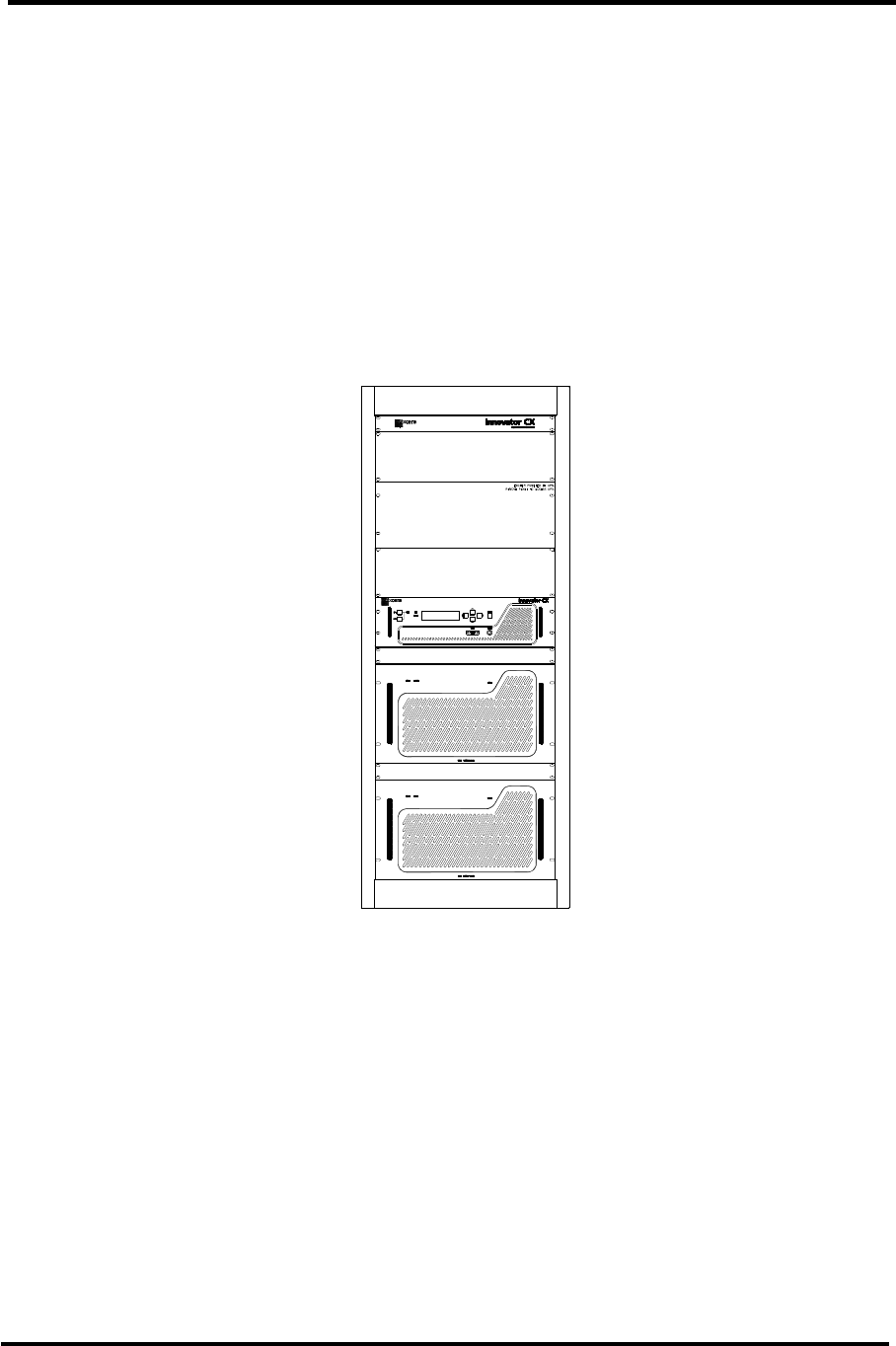
Figure 1: CHV2TD/RD Front View Typical Racking Plan
Installation
The Innovator CX series transmitters are designed for simple installation. Expensive test
equipment is not required for installation and set up and to keep a system operational. An
information decal, with Voltage Range, Current Range, Manufacturer, Model and ratings is
attached to the rear panel of the stand alone drawer or if mounted in a cabinet, to the top
of the frame above the door facing the rear of the cabinet. Prior to installing the product,
review the following items. Check that they been installed, tested and/or inspected.
Building Structure
Electrical Systems
Heating and Air Conditioning
Receive Antenna or Satellite Dish and input cabling
Optional ASI to S310 Converter, if needed
Transmit Antenna and output transmission line
A1
Exciter/Driver
A2
Power Amplifier
A3
Power Amplifier

Innovator CHV0TD/RD-1 through CHV4TD/RD ATSC Unpacking, Installation &
Transmitter/Regenerative Translator Maintenance
Instruction Manual, Rev. 1 15
The Innovator CX series systems are 17” (43.2cm) wide standard rack mountable drawers.
They are supplied with side mounted drawer Slides for ease of installation and removal.
The CHV0TD/RD-1 and CHV0TD/RD-4 systems are 3 RU, 5.25” (13.3cm) high. The external
amplifier used in CHV1TD/RD-1, CHV1TD/RD-2, and CHVTD/RD-3 systems is 9 RU 15.75”
(40cm) high, includes 3 RU 5.25” (13.3cm) for the driver and 6 RU 10.5” (26.7cm) for the
external amplifier drawer. The CHV2TD/RD systems are typically mounted in a 55”
(139.7cm) cabinet. The CHV3TD/RD and CHV4TD/RD systems are typically mounted in a
76” (193cm) cabinet. The CHV3TD/RD systems are 21 RU, 36.75” (93.3cm) high, which is
3 RU, 5.25” (13.3cm) for the driver and 18 RU, 31.5” (80cm) for the three Innovator CHV
amplifier drawers. The CHV4TD/RD systems are 27 RU, 47.25” (120cm) high, which is 3
RU, 5.25” (13.3cm) for the driver and 24 RU, 42” (106.7cm) for the four Innovator CHV
Series amplifier drawers.
Also needed for FCC compliance operation is an ATSC filter on the broadcast channel that
connects to the output of the system. Space must be provided for the ATSC filter,
combiners, reject loads, and low pass filter (if present) whose dimensions will vary
depending on manufacturer and channel. Refer to the vendor supplied information included
with your system for specific dimensions. Make sure that the space provided for the CX
series equipment is sufficient and includes the splitters, combiners, reject loads and external
filters. Check that any additional equipment, which is included in the system that extends
above or to the side of the mounting rack, has sufficient clearance space. Refer to the
custom racking plan for the system for detailed information.
Drawer Slide Installation
If the system is pre-mounted in a cabinet skip this section. Locate the drawer slides included
in the installation material for your system. See Figure 2 and the manufacturers instructions
included with the drawer slides for the cabinet mounting instructions. Install the left drawer
slide into the left side of the cabinet (as viewed from the rear). Allow 3 RU or 5.25” (13.3cm)
of space between the drawers for a CHV0xD-1 or CHV0xD-4 system. In high power systems,
allow a space of 3 RU, 5.25” (13.3cm) for the driver and 6 RU, 10.5” (26.7cm) for each of the
Innovator CHV external amplifier drawers. Space must also be provided for the splitter,
combiner, ATSC filter and low pass filter (if present). The dimensions will vary depending on
the manufacturer and the output power. Secure the left drawer slide by connecting it to the
front and rear mounting bars using No. 10 screws and the bar nuts that have been provided.
Install the drawer slide on the right side of the cabinet (as viewed from the rear) making sure
that it is aligned with the drawer slide on the left side. Secure the slide by connecting it to
the front and rear mounting bars using No. 10 screws and the bar nuts that have been
provided. Repeat this process for any other drawers if purchased. With both slides in place,
slide the drawer or drawers into the cabinet.
Figure 2: Cabinet Slides

Innovator CHV0TD/RD-1 through CHV4TD/RD ATSC Unpacking, Installation &
Transmitter/Regenerative Translator Maintenance
Instruction Manual, Rev. 1 16
AC Input Connections
The CHV0xD-1 will operate on any AC voltage from 95 – 253VAC, the CHV0xD-4 single
drawer systems will operate with an input voltage of 185-253VAC. The customer should
provide a single point disconnect for the main AC input connection to the transmitter. Check
that the AC switch located on the rear of the drawer above the AC power jack is OFF.
Connect the AC power cord supplied with the drawer from J6 on the rear of the drawer to the
AC source.
Check that the ON/OFF circuit breaker(s) for the amplifier drawer(s) located on the rear
panel on either side of the AC power jack are OFF. Connect the AC power cord(s) supplied
with the drawer(s) from J10 on the rear of the drawer to the 230 VAC source. Refer to Table
1 for typical voltage and current requirements. More detailed information refer to the system
drawings or interconnects that came with your system. Additional information will be
provided on the data label located on the rear of the rack or cabinet.
If the system is mounted in a rack an AC distribution box wired to a quad receptacle box is
used to connect the AC to the individual drawers. The AC distribution box is mounted on the
upper right side of the rack accessed through the back of the rack. The main AC input for a
transmitter is 195-253VAC, with at least 10Amps, 50/60Hz. The customer should provide a
single point disconnect for the main AC input that connects to the transmitter. The AC input
lines connect inside the AC distribution box by first removing the two screws that hold the
cover plate to the front of the AC distribution box. Then connect the three wire main AC input
to the input lugs, L1 to L1, L2 to L2 and Ground to Ground. The power amplifier drawer and
the quad receptacle box connect through AC power cords directly to the AC distribution box.
The AC power to the optional receiver drawer and the exciter/driver drawer are connected
through AC power cords that plug into the quad receptacle box.
If the system is mounted in a cabinet it may contain an AC distribution panel with breakers to
distribute the AC power to the individual drawers. The AC distribution panel is mounted
facing the rear of the cabinet and accessed through the back of the cabinet. The main AC
input for a transmitter is, 195-253VAC. The customer should provide a single point
disconnect for the main AC input that connects to the transmitter. The AC input lines connect
to the AC distribution panel by first removing the four #8 screws that hold the cover plate to
the front of the AC distribution panel. Then connect the three wire main AC input to the input
lugs located at the top left of the AC distribution panel, L1 to L1,
Innovator CHV0TD/RD-1 through CHV4TD/RD ATSC Unpacking, Installation &
Transmitter/Regenerative Translator Maintenance
Instruction Manual, Rev. 1 17
L2 to L2 and Ground to the Ground lug on the left. The AC distribution panel in a system with
two PA’s has three circuit breakers that distribute the AC to the individual drawers, which are
the Exciter and the two power amplifier drawers. The circuit breakers, which are accessed
through the rear door of the cabinet, supply the AC though AC line cords, that connect to the
AC input jacks mounted on the rear panels of the drawers. CB1 is a 30 Amp circuit breaker
which supplies the AC to the (A2), top, Power Amplifier A drawer. CB2 is a 30 Amp circuit
breaker which supplies the AC to the (A3), bottom, Power Amplifier B drawer. CB3 is a 10
Amp circuit breaker which supplies the AC to the (A1) Exciter/Driver drawer. A maximum of
four 30 Amp circuit breakers for four amplifier drawers and two 10 Amp circuit breakers for
two Exciter/Driver drawers can be installed in the AC Distribution Panel. All other systems are
configured with more or less circuit breakers to provide the protection for the AC to the
individual exciter, exciter driver and amplifier drawers.
Table 1: CHVxD series ATSC Digital Systems Typical AC Input and Current Requirements.
System O/P Power Power
Consumption Voltage Current
115 VAC 1.8 Amps
CHV0xD-1 20 Watts 200 Watts 230 VAC 1 Amp
to the
Cabinet
CHV0xD-4 200 Watts 1000 Watts 230 VAC 4.4 Amps to the
Cabinet
CHV1xD-1 400 Watts 2200 Watts 230 VAC 9.6 Amps to the
Cabinet
CHV1xD-2 600 Watts 2700 Watts 230 VAC 11.8 Amps to the
Cabinet
CHV1xD-3 850 Watts 3000 Watts 230 VAC 13.1 Amps to the
Cabinet
CHV2xD-1 1000 Watts 5100 Watts 230 VAC 22.2 Amps to the
Cabinet
CHV2xD-2 1600 Watts 7200 Watts 230 VAC 31.3 Amps to the
Cabinet
CHV3xD 2200 Watts 10000 Watts 230 VAC 43.5 Amps to the
Cabinet
CHV4xD 3000 Watts 14700 Watts 230 VAC 63.9 Amps to the
Cabinet
Exciter
Amp Cab
43.5
Amps
CHV6TD 4500 Watts 19600 Watts 230 VAC Amplifier
Cabinet
41.8
Amps
Exciter
Amp Cab
63.9
Amps
CHV8TD 6000 Watts 29000 Watts 230 VAC Amplifier
Cabinet
62.2
Amps
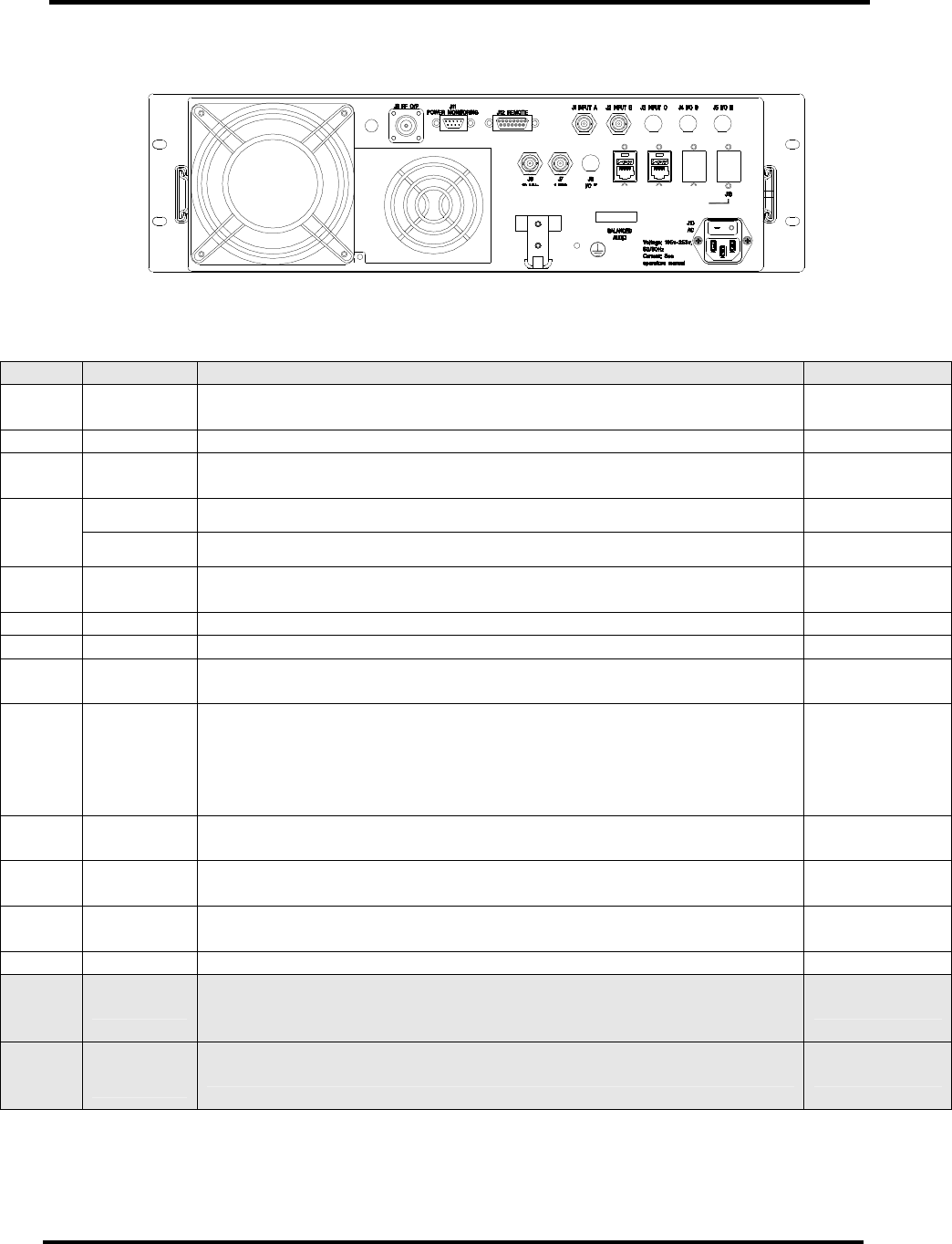
Input and Output Connections
The input and output connections to the system are made to the jacks mounted on the rear
panels of the CHV0xD-1 and CHV0xD-4 systems. Each exciter/driver will accept a SMPTE-
310 or ASI (BTD) input and output a digital RF ON Channel signal. Refer to Tables 2 & 2A
that follow for the locations and information on the jacks and connectors.
Innovator CHV0TD/RD-1 through CHV4TD/RD ATSC Unpacking, Installation &
Transmitter/Regenerative Translator Maintenance
Instruction Manual, Rev. 1 18
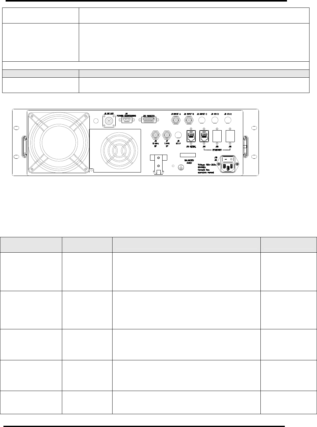
Figure 2A: Rear View CHV exciter/driver
Table 2A: Connections for the CHV20B, CHV200B and the driver for the CHV400B & higher
power systems
Port Type Function Impedance
J1 BNC Input A: On Channel RF Input (BRD) –75 to –8 dBm or SMPTE-
310 Input/ASI (TD) 50 Ohms
J3 BNC Pre-filter sample for DM8C modulator. -10 to +10 dBm 50 Ohms
J4 BNC SMPTE-310 Output (RD Only) Normally jumpered to J5. Post-
filter sample for DM8C modulator. -10 to +10dBm 50 Ohms
BNC SMPTE-310 Input (RD Only) Normally jumpered to J4. 50 Ohms
J5
TNC GPS Antenna Input (Only used with Internal GPS Kit) 75 Ohms
J6 BNC 10 MHz Input: Optional External 10 MHz Reference Input or 10
MHz input from J12 on Axciter Drawer. 50 Ohms
J7 BNC 1 PPS Input: Optional External 1 PPS Reference Input 50 Ohms
J9 N RF Output: On Channel RF Output 50 Ohms
J10 IEC AC Input: AC input connection to 85-264VAC Source and
On/Off circuit breaker N/A
J11 9 Pos
Male D
Power Monitoring: Interface to System and external amplifier
drawers, if present. Also provides an interlock for the Reject
Load (if used). If not used, in systems with no external
amplifier, a jumper from J11-6 to J11-9 needs to be in place.
Refer to Table 2B which follows for information on connections.
N/A
J12 15 Pos
Female D
Remote: Remote control and status indications. Refer to Table
7A on pages 27 & 28 for information on the connections. N/A
J13 RJ-45 Serial: Provides communication to System and to external
amplifier drawers, if present. N/A
J14 RJ-45 Ethernet: Optional Ethernet connection. May not be present in
your drawer. N/A
J15
Front
Panel
BNC
RF Sample: Output Sample from Output Detector Board.
In a CHV200B the sample level at J15 is approximately 60dB
down from the output power level of the drawer.
50 Ohms
J16
Front
Panel
9 Pos
Female D Serial: Used to load equalizer taps into the modulator. N/A
NOTES: 1) If your system contains an Optional ASI to S310 Converter, connect the ASI
output of the STL to the ASI in jack on the rear panel of the converter. Connect
the SMPTE-310 Output from the SMPTE 310 Out jack on the rear panel of the
converter module to the input jack J1 on the rear panel of the exciter/driver.
J1
J2
J11
J12
J10
J6
J9
J
7
J13
J14
J
4 J5
Innovator CHV0TD/RD-1 through CHV4TD/RD ATSC Unpacking, Installation &
Transmitter/Regenerative Translator Maintenance
Instruction Manual, Rev. 1 19
2) If your system contains an Optional K-Tech receiver, connect the RF from the
receive antenna or one output of the splitter to the input jack J1 on the rear panel
of the K-Tech receiver. Connect the SMPTE-310 Output from the SMPTE 310 Out
jack J2 on the rear panel of the K-Tech receiver to the input jack J5 on the rear
panel of the exciter/driver Drawer. 3) If the system contains the optional K-Tech
back up system, the K-Tech receiver is bypassed by using the second output of the
splitter that connects to J1 on the rear panel of the exciter/driver and connecting a
jumper from J4 to J5, after removing the cable from the K-Tech receiver, on the
rear panel of the exciter/driver. This configuration uses the 8VSB demodulator
board in the exciter/driver drawer to produce the SMPTE-310 signal.
J11 Power Monitoring Connections
In systems with one or more external amplifiers, J11 is used to communicate the output
forward and reflected metering voltages back to the driver. J11 is connected directly to the
external amplifier when there is only one external amplifier and is connected through the
system metering module when multiple external amplifiers are used. In multiple external
amplifier systems there are thermal switches mounted on the reject loads of the combiner,
and the Reject load interlock is connected to the thermal switches and is used to shut down
the system if the reject load overheats. In systems with no external amplifier, the only
connection used is the Reject Load Interlock, which must be connected to Supply Return
using a jumper from J11-6 to J11-9.
Table 2B: J1 9 Pos Male “D” Connector
J11
Pin Function
1 +12VDC
2 System Forward Power
3 System Reflected Power
4 System Aural Power
5 Remote Spare Input
6 Reject Load Interlock. (If not used, in systems with no external amplifier, must
be jumpered to J11-9)
7 System Serial +
8 System Serial -
9 Supply Return (If Reject Load Interlock is not used, in systems with no external
amplifier, must be jumpered to J11-6)
Innovator CHV0TD/RD-1 through CHV4TD/RD ATSC Unpacking, Installation &
Transmitter/Regenerative Translator Maintenance
Instruction Manual, Rev. 1 20
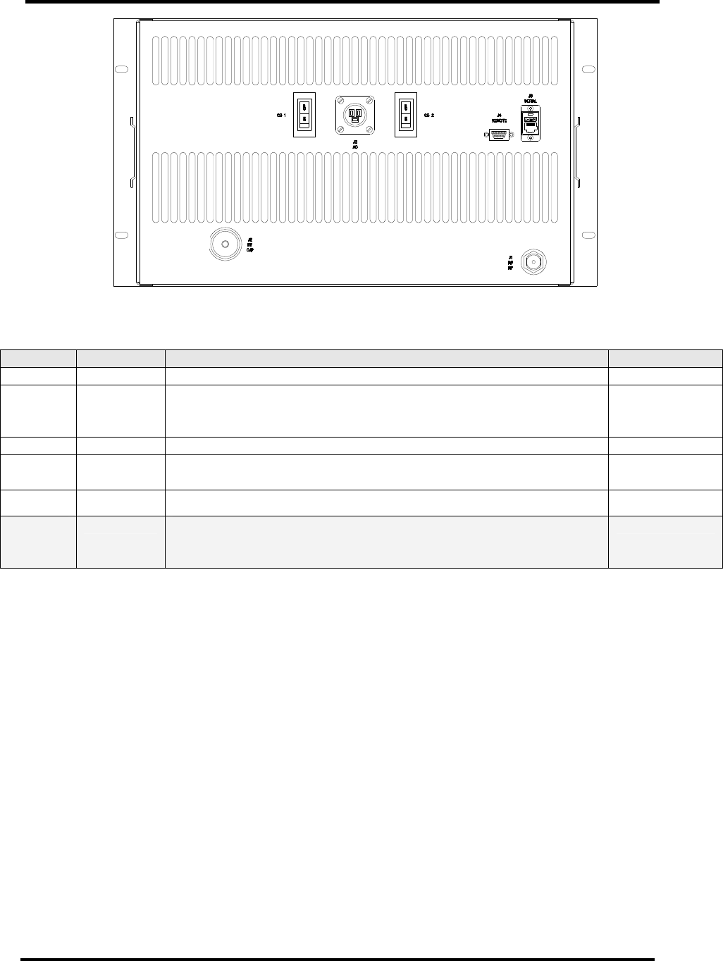
Figure 4: Rear View CHV External Amplifier Drawer
Table 3: Connections for the External Amplifier Drawer
Port Type Function Impedance
J1 N RF Input: On Channel RF from CHVB driver drawer 50Ω
J2
7/16”
(1.1cm)
Din
RF Output: On Channel RF Output 50Ω
J3 IEC AC Input: AC input connection to 230VAC Source N/A
J4 9 Pos D Remote: Amplifier Control Interface
(Connects to J11 on the exciter/driver drawer) N/A
J5 RJ-45 Serial data N/A
J8
Front
Panel
BNC
RF Sample: Output Sample from Combiner thru Control
Board. In a CHV500B, the sample level is approximately
70dB down from the output power level of the drawer.
50Ω
If used, connect the external 10 MHz reference input to the 50Ω BNC 10 MHz input jack J6
located on the rear panel of the exciter/driver. If used, connect the external 1 PPS
reference input to the 50Ω BNC 1 PPS input jack J7 located on the rear panel.
In Regenerative Translator (RD) systems there may be a SMPTE-310 loop-thru from the
output of the Demodulator Board at J4, mounted on the rear panel of the transmitter or
driver drawer to the input to the Modulator Board at J5 mounted on the rear panel of the
transmitter. There is normally a jumper installed from J4 to J5. To feed SMPTE-310 directly
to the Modulator Board remove the jumper and insert SMPTE-310 into J5. This is only used
in Translator (RD) systems not Transmitter (TD) systems.
The digital RF ON Channel output of the exciter/driver is at J9 the 50Ω “N” connector RF
output jack located on the rear panel. The output of the drawer at J9 connects to the low
pass (if present) digital mask filter and then to the antenna for your system. In higher
power systems the output of the driver drawer at J9 is connected to J1 the 50 Ohm “N”
connector RF input jack located on the rear panel of the external amplifier or to a splitter in
multiple amplifier systems. In systems with one external amplifier, check that the system
power metering interface cable is connected from J11 the 9 position “D” connector located
on the rear panel of the driver drawer to J4 the 9 position “D” connector located on the rear
panel of the amplifier drawer. This cable provides the control, status and operating
parameters of the amplifier drawer to the driver drawer. In systems with more than one
J
1
J
3
J
4
J
2
CB1
CB2
J5

Innovator CHV0TD/RD-1 through CHV4TD/RD ATSC Unpacking, Installation &
Transmitter/Regenerative Translator Maintenance
Instruction Manual, Rev. 1 21
external amplifier, the output of the driver drawer is split and connected to J1 the “N” type
connector RF input jack on the amplifier drawers. Check that the system power metering
interface cable is connected from J11 the 9 position “D” connector located on the rear panel
of the driver drawer to J9 the 9 position “D” connector located on the System Metering
Board. Also check that the serial connection is cabled from the RJ-45 connector J13 on the
driver drawer to the RJ-45 connector J1 on the system metering board. The system
metering board provides serial RJ-45 connections at J2 and J5 that are cabled to the RJ-45
serial port J5 on the rear panel of the amplifier drawers. These cables provide the control,
status and operating parameters of the amplifier drawers to the driver drawer through the
System Metering Board.
The digital RF ON Channel output of the amplifier drawer is at J2 the 50Ω 7/16 DIN
connector RF output jack located on the rear panel that connects directly to the digital mask
filter, the low pass filter (if present) and then to the antenna for your system in single
amplifier systems. In multiple amplifier drawer systems the outputs of the drawers connect
to a combiner and then the digital mask filter, the low pass mask filter (if present), the
output coupler and finally to the antenna for your system. The output coupler provides
forward and reflected power samples that are cabled to the System Metering Board at J8
reflected and J3 forward. Also connected to the system metering board at J10-6 & 9 is the
output of the over-temperature switch mounted to the reject load that is used as the reject
interlock by the system. The samples and interlock are fed through J9 on the system
metering board to J11 on the driver drawer.
This completes the connections of the system.
Maintenance
Innovator CX series transmitters are designed with components that require little or no
periodic maintenance except for the routine cleaning of the fans and the front panels of the
modules and the periodic check of general tightness of hardware.
It is recommended that periodically, the time interval depends on the amount of movement
the cabinet receives, all mounting hardware, holding drawer slides, shelving and mounting
plates inside the cabinet are checked for tightness. All screws and bolts that are accessible
should be tightened initially when the transmitter is received and periodically thereafter if the
transmitter is moved by vehicle. All coaxial connectors, hard-line connections and hardware
holding combiners, splitters, or any other mounted items should be checked and tightened.
The amount of time between cleanings of the drawers and cabinets depends on the conditions
within the transmitter room. While the electronics have been designed to function even if
covered with dust, a heavy buildup of dust, dirt, or insects will affect the cooling of the
components. This could lead to a thermal shutdown or the premature failure of the affected
drawer. When the front panels of the drawers become dust covered, the drawer should be
pulled out and any accumulated foreign material should be removed.
NOTE: To remove the CX series transmitter from the cabinet, the input and output cables
must be removed from the rear of the transmitter before the drawer can be pulled out
completely from the cabinet.
A vacuum cleaner, utilizing a small, wand-type attachment, is an excellent way to suction out
any dirt from the drawer and cabinet. Alcohol and other cleaning agents should not be used
unless you are certain that the solvents will not damage components or the silk-screened
markings on the drawers and boards. Water-based cleaners can be used, but do not saturate
the components. The fans and heatsinks should be cleaned of all dust or dirt to permit the
free flow of air for cooling purposes. It is recommended that the operating parameters of the

Innovator CHV0TD/RD-1 through CHV4TD/RD ATSC Unpacking, Installation &
Transmitter/Regenerative Translator Maintenance
Instruction Manual, Rev. 1 22
transmitter be recorded from the LEDs and the LCD system metering on the front panel of the
drawer at least once a month to be used for comparison purposes in case of a failure. It is
suggested that this data be retained in a rugged folder or envelope and stored near the
transmitter.

Innovator CHV0TD/RD-1 through CHV4TD/RD ATSC Unpacking, Installation &
Transmitter/Regenerative Translator Maintenance
Instruction Manual, Rev. 1 23
This page has intentionally been left blank.

Innovator CHV0TD/RD-1 through CHV4TD/RD ATSC
Transmitter/Regenerative Translator w/DM8C Modulator Interface Description
Instruction Manual, Rev. 1 24
Initial On-Site Turn On Procedure
After the Innovator CHV series drawer or drawers are installed and all input, output
and AC connections are made, the system is ready for the initial on site turn on.
Check that the output of the exciter/driver drawer is connected to an appropriate
rated load or to the digital mask filter, low pass filter (if present), and the antenna
for your system. If your system contains external amplifiers, check that the output
of the amplifier drawer or the combiner assembly is connected to an appropriate
rated load or to the digital mask filter and the antenna for your system. Check that
the main AC power to the System is ON. NOTE: If your system is mounted in a
cabinet and contains an Optional UPS, turn on the UPS.
Locate the exciter/driver drawer and push ON the switch located on the rear panel of
the transmitter near the AC power jack. The fan mounted on the rear panel of the
drawer should operate when the AC is applied. If your system contains external
amplifiers, push ON the switch located on the rear panel of the driver drawer and also
switch ON the ON/OFF circuit breaker(s) located on the rear panel of the amplifier
drawer(s) mounted on each side of the AC input power jack. The small fan mounted
on the rear panel of the driver drawer should operate and the two fans mounted in
the amplifier drawer should operate when AC is applied. The large fan mounted in the
rear panel of the system or driver drawer will operate when the A10 switching supply
is enabled.
Place the system into Operate. The Operate/Standby LED and Status LEDs on the
exciter/driver should be Green indicating the system is in Operate and performing
normally. Both fans (Note: Some models may only have one fan on the exciter/driver)
should be operating. The Operate/Standby LED showing Amber indicates the System
is in Standby. The Status LED showing a blinking Red LED indicates an Event (Fault)
is occurring now. The Status LED showing Amber indicates that an Event (Fault)
occurred since the last time the Event (Fault) indications were reset.
If your system contains external amplifiers the Enable LED and Status LEDs on the
amplifier drawer should be Green indicating the system is in Operate and performing
normally. The Enable LED showing Amber indicates the System is in Standby. The
Status LED should be Green indicating no Events (Faults) in the system. If the
Operate/Standby LED shows Amber it indicates that the System is in Standby. If the
Status LED is blinking Red it indicates an Event (Fault) is occurring now. If the Status
LED shows Amber it indicates that an Event (Fault) occurred since that last time the
Event (Fault) indications were reset. The output power is factory set according to
customer request and does not need adjusted. If a problem occurs, call Axcera field
support at 724-873-8100 for information on modifying the power level of the
system.
NOTE: The RF System Interlock is provided on J12, a 15 position “D” connector,
located on the rear panel of the exciter/driver. The RF System Interlock at
J12-5 provides the customer with a means of connecting the system to
protection circuits, for the loads, thermal switches, combiners, or the
antenna, in the output of your system, that will place the system in Standby
if the protection circuit opens. The Reject Load Interlock is provided at J11,
a 9 position “D” connector. J11-6 provides the customer with a means of
connecting the system to protection circuits, for the reject load in multiple
amplifier systems, which will place the system in Standby if the protection
circuit opens. If the interlocks are not used in your system, a plug with a
jumper from J12-5 to J12-15, ground, for RF system Interlock and another
Innovator CHV0TD/RD-1 through CHV4TD/RD ATSC
Transmitter/Regenerative Translator w/DM8C Modulator Interface Description
Instruction Manual, Rev. 1 25
plug with a jumper from J11-6 to J11-9, for Reject Load Interlock, need to
be connected. These jumpers provide the RF System and Reject Load
Interlocks, which allow the system to go to operate. Without the jumpers,
the system will remain in Standby.
Typical System Operating Parameters
Typical Operating Parameters for a CHV0TD-1
Parameter Typical Reading
Forward Power 100%
Reflected Power <5%
Power Supply Voltage 48 Volts
Heatsink Temperature 20º to 30º F/15º to 20º C above ambient
temperature
Pin Attenuator Voltage 1 Volt to 5 Volts
Typical Operating Parameters for a CHV0TD-1 used as driver
Parameter Typical Reading
Forward Power 20-70% (Depending on output power level of
system)
Reflected Power <5%
Power Supply Voltage 48 Volts
Heatsink Temperature 20º to 30º F/15º to 20º C above ambient
temperature
Pin Attenuator Voltage 1 Volt to 5 Volts
Typical Operating Parameters for a CHV0TD-4
Parameter Typical Reading
Forward Power 100%
Reflected Power <5%
Power Supply Voltage 48 Volts
Heatsink Temperature 20º to 30º F/15º to 20º C above ambient
temperature
Pin Attenuator Voltage 1 Volt to 5 Volts
Typical Operating Parameters for a CHV0TD-4 used as a Driver
Parameter Typical Reading
Forward Power 20-70% (Depending on output power level of
system)
Reflected Power <3%
Power Supply Voltage 48 Volts
Heatsink Temperature 20º to 30º F/15º to 20º C above ambient
temperature
Pin Attenuator Voltage 1 Volt to 5 Volts
Typical Operating Parameters for the external Amplifier Drawer(s)
Parameter Typical Reading
Forward Power 100%
Reflected Power <5%
Power Supply Voltage 48 Volts
Heatsink Temperature 77º to 104º F/25º to 40º C above ambient

Innovator CHV0TD/RD-1 through CHV4TD/RD ATSC
Transmitter/Regenerative Translator w/DM8C Modulator Interface Description
Instruction Manual, Rev. 1 26
temperature
Innovator CHV0TD/RD-1 through CHV4TD/RD ATSC
Transmitter/Regenerative Translator w/DM8C Modulator Interface Description
Instruction Manual, Rev. 1 27
Typical Problems, Indications and Causes in Exciter/Driver Drawer
Problem Indication Cause
No power to
drawer
Operate/Standby and Enable LED
indicators and LCD display are Off
AC power cord not connected.
Main AC to System missing.
On/Off switch on back of drawer
Off. 10 Amp fuse (F1) blown*.
Power supply (A9) not operating
No Output
Signal
Front Panel Status LED is Amber
and blinking with no events, faults
indicated.
On the 8VSB Modulator S310
MPEG Input Selection Set Up
Screen, the Input is currently set
incorrectly to “from Internal
Source”. Set to “from External
Source”. (Not used with Axciter)
Loss of Input
Signal Loss of Input on Modulator Menu Loss of input signal.
(Not used with Axciter)
Loss of
Output
Signal
Amber Operate/Standby LED.
Blinking Red Status LED.
Any Event, Fault, which Mutes
the output. Including Input
Fault, VSWR Cutback, Overdrive,
Over-temperature and
Overvoltage.
Loss of 48V Power Supply Fault on Power
Supply Menu
Power supply (A10) not
operating
Loss of ±12V
or 5V
Operate/Standby and Enable LED
indicators and LCD display are Off Power supply (A9) not operating
NOTE: *A spare 10 Amp fuse is provided in the blank fuse holder under the
active fuse.
If there is an Event (Fault) occurring in the system, the Status LED on the front
panel will flash RED as long as the Event (Fault) is present. In addition, the menu
will jump to the current Event (Fault) on the display and blink the Event (Fault)
continuously, if the Jump to Fault screen is set to Yes. When the Event (Fault) is
corrected, the drawer will turn the Status LED to AMBER to indicate that there was a
Fault and the menu will still display the Fault but it will not flash. This gives the user
the knowledge that there was an Event (Fault) and what type of Event (Fault)
occurred. Before clearing the fault, check if there were other Events (Faults) by
stepping through the menus. To reset the indication of previous Events (Faults) the
user must push the Enter button with the Event (Fault) Reset Screen displayed. This
will reset all previous Events (Faults).
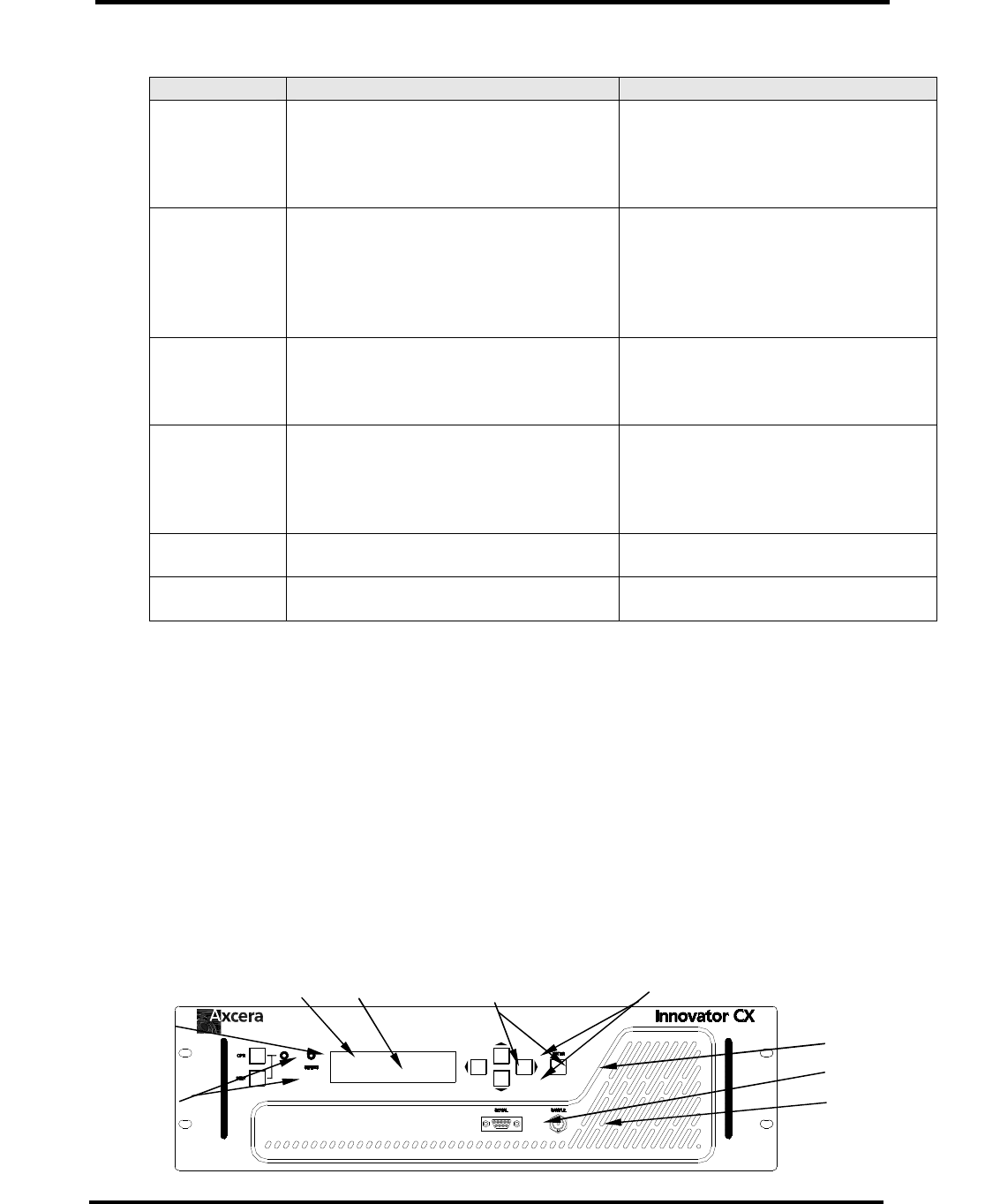
LCD Display and Front Panel LED Indicators
Operate/Standby
Buttons
Status LED
Left/Right Buttons
LCD Display
Enter Butt
on
Operate/Standby
LED
Up/Down Buttons
J11 Serial Port
J15 RF Sample
Innovator CHV0TD/RD-1 through CHV4TD/RD ATSC
Transmitter/Regenerative Translator w/DM8C Modulator Interface Description
Instruction Manual, Rev. 1 28
Figure 5: Front View Innovator Cx exciter/driver
Table 4: Innovator CX Series LCD Display
DISPLAY FUNCTION
LCD Provides a two line readout of the input received channel, internal
functions, status, and Fault (Event) conditions.
The front panel has seven pushbuttons, two for the control of the system, Operate &
Standby, and five for control of the displayed menus, Left, Right, Up, Down & Enter.
Table 5: Innovator CX Series Control Pushbuttons
PUSHBUTTON FUNCTION
OPR When pushed switches the system to Operate.
STBY When pushed switches the system to Standby.
ENTER Selects the changes made in the menus and submenus.
Up & Down Arrow Scrolls through the main menus and after entering the Main Menu
Steps through submenus of the main menu when they are present.
Left & Right Arrow Used to exit from main menus and submenus of the main menu
when they are present.
Table 6: Innovator CX Series Operate/Standby and Status Indicators
LED FUNCTION
OPERATE/STANDBY
(Green/Amber)
A Green LED indicates that the system is in Operate. An Amber
LED indicates that the system is in Standby.
STATUS
(Green/Red/
Amber)
A Green LED indicates that the system is functioning normally. A
flashing Red LED indicates an Event (Fault) is occurring at this
time. An Amber LED indicates an Event (Fault) occurred since
the last time the Event (Fault) indications were reset but the
system is now operating normally. Amber LED Blinking, with no
Events (Faults) indicates the MPEG input is set to Internal Source.
NOTE: J15 is a Front Panel BNC RF Sample Jack 50Ω that provides an RF output
sample from the output detector board in the drawer. In a CHV200B, the
sample level at J15 is approximately 60dB down from the output power level
of the drawer.
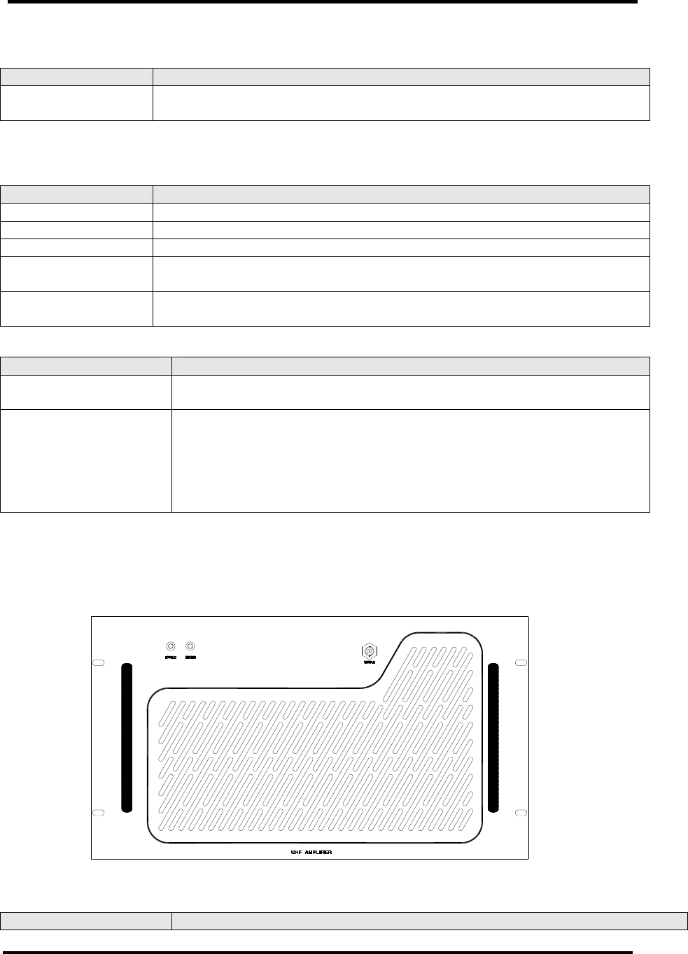
Figure 6: Front view of the external amplifier drawer
Table 7: Innovator CHV Amplifier Drawer LED Indicators and Sample Jack
LED FUNCTION
Enable LED
Status LED
Sample
Innovator CHV0TD/RD-1 through CHV4TD/RD ATSC
Transmitter/Regenerative Translator w/DM8C Modulator Interface Description
Instruction Manual, Rev. 1 29
ENABLE
(Green/Amber)
A Green LED indicates that the system is in Operate and operating
normally. An Amber LED indicates that the system is in Standby.
STATUS
(Green/Red/
Amber)
A Green LED indicates that the system is functioning normally with no
faults. A flashing Red LED indicates an Event (Fault) is occurring at
this time. An Amber LED indicates an Event (Fault) occurred since the
last time the Event (Fault) indications were reset but the system is now
operating normally.
JACK FUNCTION
SAMPLE
J6
Typical sample value is 65dB down from the output power level of the
drawer. (500 Watts output power = -8dBm sample level)
System Remote Connections to J12
Figure 7: Rear View Innovator Cx exciter/driver
The remote connections for the Innovator CHV series system are made to the
Remote 15 Pos Female “D” connector Jack J12 located on the rear panel of the
drawer.
Table 7A: Remote Connections to J12 15 Pos Female D Connector for Innovator CX
series system
Remote Signal
Name
Pin
Designation Signal Type Description
System Operate J12-1
Discrete Open Collector Input - A pull down
to ground on this line indicates that the
System is to be placed into the operate
mode.
(Low = Activate : Floating = No Change)
Command
System Standby J12-2
Discrete Open Collector Input - A pull down
to ground on this line indicates that the
System is to be placed into the standby
mode.
(Low = Activate : Floating = No Change)
Command
Power Raise J12-3
Discrete Open Collector Input - A pull down
to ground on this line indicates that the
Power of the System is to be Raised.
(Low = Activate : Floating = No Change)
Command
Power Lower J12-4
Discrete Open Collector Input - A pull down
to ground on this line indicates that the
Power of the System is to be Lowered.
(Low = Activate : Floating = No Change)
Command
System Interlock J12-5
Discrete Open Collector Input - A pull down
to ground on this line indicates that the
Interlock is present. Normally jumpered to
J12

Innovator CHV0TD/RD-1 through CHV4TD/RD ATSC
Transmitter/Regenerative Translator w/DM8C Modulator Interface Description
Instruction Manual, Rev. 1 30
Remote Signal
Name
Pin
Designation Signal Type Description
J12-15. (Low = OK : Floating = Fault)
Set to
Modulation Type J12-6
Discrete Open Collector Input. - Sets the
Modulation type of the system.
(Low = Analog : Floating = Digital)
Command
Set Channel
(Set Up 1 or Set
Up 2)
J12-7
Discrete Open Collector Input. – Selects one
of two possible Channel Setups of the
system.
(Low = Set Up 2, CH 2 : Floating = Set Up
1, CH 1) NOTE: The Set Up 1 & Set Up 2
settings are displayed and changed in the
Upconverter Set Up Menus.
Command
Ground J12-8 Ground.
System Forward
Power Level
(See NOTE at
end of table)
J12-9
Analog Output - 0 to 4.0 V. - This is a
buffered loop through of the calibrated
“System Forward Power”. Indicates the
System Forward power.
Scale factor is 100 % = 2.0V.
Metering
System Aural
Power Level
(See NOTE at
end of table)
J12-10
Analog Output - 0 to 4.0 V. - This is a
buffered loop through of the calibrated
“System Aural Power”. Indicates the
System Aural power. Scale factor is
100 % = 2.0V. (Not used in Digital)
Metering
System Reflected
Power Level
(See NOTE at
end of table)
J12-11
Analog Output - 0 to 4.0 V. - This is a
buffered loop through of the calibrated
“System Reflected Power”. Indicates the
System Reflected power.
Scale factor is 25 % = 2.0V.
Metering
Report Input
Status J12-12
Discrete Open Collector Output. - Indicates
if input to system is Normal or Not.
(Low = OK : Floating = Fault)
Status
Report Fault
Status J12-13
Discrete Open Collector Output. - Indicates
if system is Operating Normally or has a
Fault.
(Low = OK : Floating = Fault)
Status
Report Operate
Status J12-14
Discrete Open Collector Output. – Indicates
whether system is in Operate or Standby.
(Low = Operate : Floating = Standby)
Status
Ground J12-15 Ground. Normally jumpered to J12-5.
NOTE: The analog remote metering functions are scaled such that 2V = a known power. The
forward power is typically scaled so that 2V = 100%, and the reflected is scaled such that 2V =
25%. These voltages are generated by detecting the RF voltage, and the change is proportional
to the RF voltage change, rather than proportional to the change in RF power. There is a direct
relationship between changes in RF power and RF voltage, as the Power change is proportional
to the square of the voltage change, (P=V2/R).
Example: Output power is scaled so that 2V = 100%. To calculate the power for 1V, take
(1V/2V)2 x 100% = 25%.
Most remote control systems are set up to handle this format directly and will do the calculations
required to scale the displayed power appropriately.

Innovator CHV0TD/RD-1 through CHV4TD/RD ATSC
Transmitter/Regenerative Translator w/DM8C Modulator Interface Description
Instruction Manual, Rev. 1 31
Innovator CHV0TD/RD-1 through CHV4TD/RD ATSC
Transmitter/Regenerative Translator w/DM8C Modulator Interface Description
Instruction Manual, Rev. 1 32
LCD Front Panel Screens
A LCD display, located on the front of the Innovator Cx series systems displays the
current operating status of the system. When the drawer is powered On the LCD will
initially display two splash screens. The first splash screen will be displayed for a few
seconds, then the second splash screen will be displayed for a few seconds and
finally the RF Power Display default screen will be displayed. See examples of the
screens below. NOTE: These screens are typical examples; your systems screens
may be different. The RF Power Display default screen will be the screen displayed
if no buttons are pushed to access other screens. While viewing the RF Power
Display default screen, pushing the Left and Right arrow buttons together will also
access the splash screens. NOTE: In dual exciter systems, the On Air Exciter will
display the operating parameters of the system.
Splash Screen Number 1
The first splash screen displayed indicates the manufacturer, type and the model
number.
Shown are P/N: 1316306 firmware version level 2.0b and EPLD version 2.5.
The following screens are scrolled through using the buttons to the right of the display.
Pushing and releasing the Up & Down Arrows will scroll you through the Main Menus,
which are shown on the following pages aligned on the left side of the page. The
Submenus of the Main Menus are accessed by pushing and releasing the ENTER
button. Once in the Submenus, pushing and releasing the Up & Down Arrows will
scroll you through the submenus of the Submenus. The Submenus are shown on the
following pages indented under the Main Menus and the submenus of the Submenus
are indented under the Submenu in which they are contained. In the SET UP Menus,
changes are made to the display by Pushing and releasing the ENTER button which
causes the item to be changed to blink, then using the left and right arrow buttons to
display the desired changed item, finally, pushing the ENTER button will accept the
changes made upon exit of the Set Up Menu.
NOTE: An example of accessing and changing an item using the Set Up Menus is as
follows. This procedure is to set the Off Air Receive Channel to the desired
channel. Push and release the DOWN Arrow button until the SYSTEM SET UP
Main Menu is displayed. Push and release the ENTER button. The
Authorization Warning screen is displayed. Push and release the ENTER
Left/Right Buttons
Enter Button
Up/Down Buttons
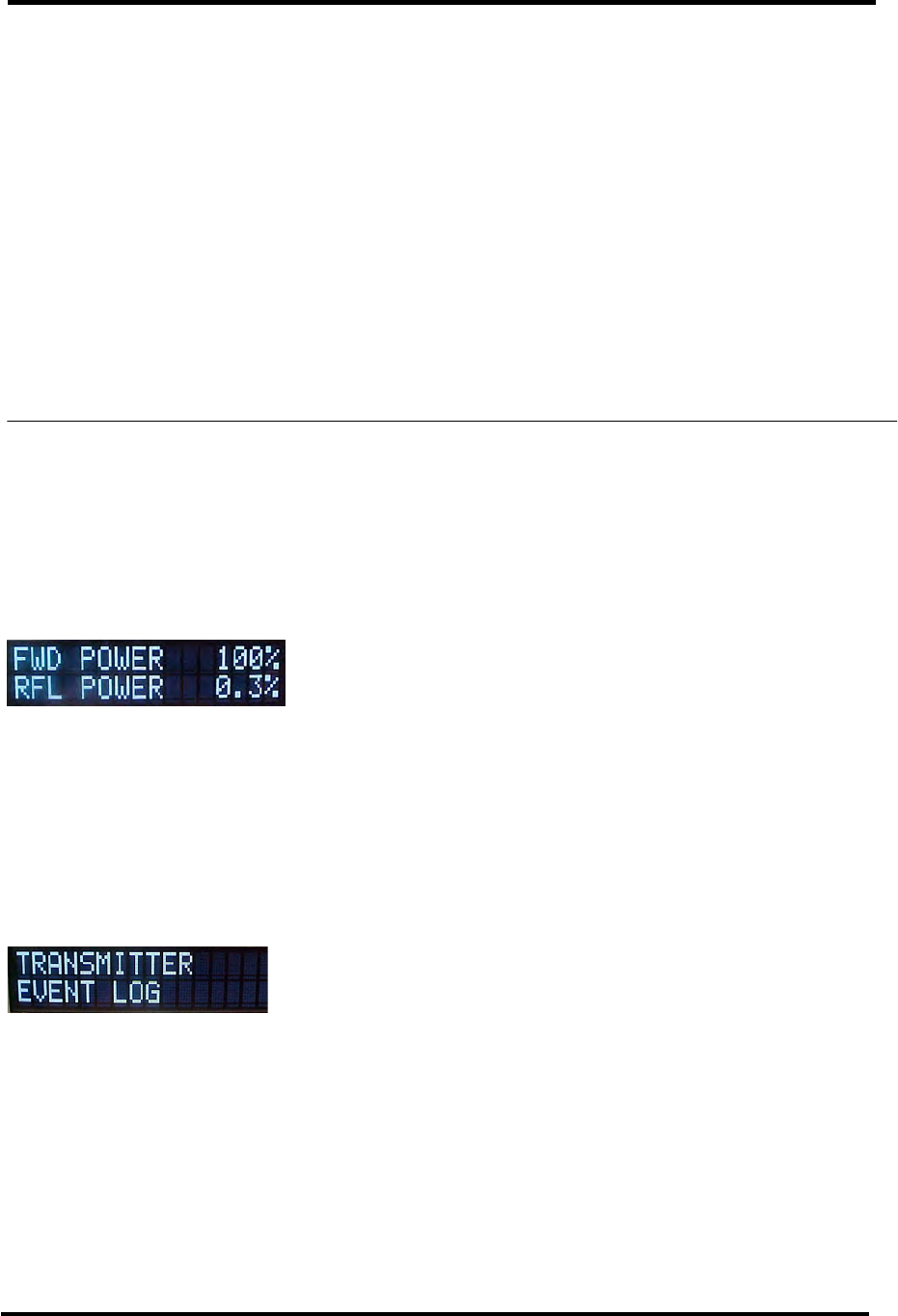
Innovator CHV0TD/RD-1 through CHV4TD/RD ATSC
Transmitter/Regenerative Translator w/DM8C Modulator Interface Description
Instruction Manual, Rev. 1 33
button again and the ENTER BUTTON SETS TO CHANGE MODE screen is
displayed. Push and release the ENTER button again and the first set up
menu, which is the SET UP MENUS OF CHASSIS VALUES screen is displayed.
Push and release the DOWN Arrow button until the SET UP 8VSB
DEMODULATOR screen is displayed. Push and release the ENTER button to
display the submenus under the SET UP 8VSB DEMODULATOR menu. Push
and release the DOWN Arrow until the 8VSB DEMODULATOR USE OFF AIR
CHxx is displayed. Push and release the ENTER button and the XX, which
indicates the Channel Number, will blink. Push and release the UP or DOWN
Arrow button until the desired new channel number is displayed. Push and
release the ENTER button, and the PUSH ENTER TO ACCEPT CHANGES menu
is displayed. Push and release the ENTER button again to accept the changes
made. The channel is now changed. Push and release the LEFT Arrow to exit
to the SET UP 8VSB DEMODULATOR screen. Push and release the LEFT Arrow
again to exit to the SYSTEM SET UP Main Menu. Push and release the UP or
DOWN arrows to browse the main menus.
The following screens are typical of an operating system. The values indicated on
the screens in your system may vary from those shown below.
Operation Screens
NOTE: The following Operation screens provide operating information only. No
adjustments are available using these screens.
Figure 9: Transmitter/Translator RF Power Screen (TD/RD)
Menu Level This is the default screen that is displayed after the splash
screens are displayed.
Description This screen provides an indication of the Forward Output Power
of the system in terms of Percent. (Typically 100%). The screen
also provides an indication of the Reflected Power of the system
in terms of Percent. (Typically less than 5%)..
Push the DOWN Arrow to view the next main menu, which is the Transmitter Event
Log Main Menu.
Figure 10: Transmitter/Translator Event Log Main Screen (TD/RD)
Menu Level System Main Screen.
Description This is the Transmitter Event Log Main Screen. Push the ENTER
button to access the Event List submenu.
Push the DOWN Arrow to view the next main menu, which is the Transmitter Details
Main Menu.
Innovator CHV0TD/RD-1 through CHV4TD/RD ATSC
Transmitter/Regenerative Translator w/DM8C Modulator Interface Description
Instruction Manual, Rev. 1 34
Figure 10.1: Transmitter/Translator Event List Screen (TD/RD)
Menu Level System Event Log Sub Screen.
Description When events occur, they will be displayed on this screen. The
Up and Down arrow will page you through the different entries
in the event log. The above screen indicates the 001 event of
013 total events that have occurred in the Transmitter. The
number in the parenthesis on the top right, is this case 01,
indicates the number of time
s the displayed event has occurred.
The bottom line scrolls to indicate the event that occurred, in
this case RF Interlock Fault. NOTE: When the Date & Time are
available, this information is displayed for the event, otherwise
the Time Interval between events is displayed.
Push the LEFT Key to exit to the Transmitter Event Log Main Menu screen. Pushing
the
RIGHT Key will access the Event Reset Screen.
Figure 10.2: Event Reset Screen (TD/RD)
Menu Level System Event Log Sub Screen.
Description This screen allows the resetting of the event log, after they are
observed or corrected. NOTE: Resetting the events on an
amplifier may cause the transmitter to momentarily mute.
Figure 10.3: Event Reset Old Faults Screen (TD/RD)
Menu Level System Event Log Sub Screen.
Description This screen allows the resetting of old faults that are latched
from the event log after they are observed or corrected. The
transmitter can be configured to latch faults as detailed in
Figure 11.1.4. That means that if a fault occurs and then it
clears, the status of the parameter in the details screen will not
blink indicating an active fault, but it will still show fault
indicating that previously this parameter was faulted. Within
the web pages, a latched fault is shown with an orange
background while faulted parameters are shown in red and good
values are shown in green. Resetting Old Faults will clear the
latched fault and the display will show the value as OK or with
other text that indicates that it is not faulted.
Innovator CHV0TD/RD-1 through CHV4TD/RD ATSC
Transmitter/Regenerative Translator w/DM8C Modulator Interface Description
Instruction Manual, Rev. 1 35
Figure 11: Transmitter/Translator Details Main Screen (TD/RD)
Menu Level System Main Screen.
Description This is the System Details Main Screen. Push the ENTER button
to access the Device Details Chassis Values Main Sub Screen.
Push the DOWN Arrow to view the next main menu, which is the System Set Up Main
Menu.
Figure 11.1: Transmitter/Translator Device Details Exciter Values Screen (TD/RD)
Menu Level System Device Details Exciter Values Main Sub Screen.
Description Push the ENTER button to access the Device Details Exciter
Values submenus or push the DOWN Arrow to view the next
main submenu, which is the ATSC Modulator Sub Menu
Device Details Screens - These are read only parameters.
Figure 11.1.1: Transmitter/Translator Driver Forward/Reflected Power Details
Screen (TD/RD)
Menu Level System Device Details Exciter Values Driver Sub Screen.
Description This screen provides an indication of the Output Forward
Power of the Driver Drawer in terms of Percent, typically 20-
70%. This screen also provides an indication of the Reflected
Output Power of the Driver Drawer in terms of Percent,
Typically less than 3%.
Figure 11.1.2: Heatsink Temperature Details Screen (TD/RD)
Menu Level System Device Details Exciter Values Driver Sub Screen.
Description This screen indicates the temperature of the amplifier heatsink
assembly, mounted in the system or driver drawer, in degrees
Fahrenheit or Centigrade. If the temperature is below the trip
point, it will indicate OK. (Typically 20º to 30º F. or 15º to 20º
C above ambient temperature.)
Figure 11.1.3: Power Supply Voltage Details Screen (TD/RD)
Menu Level System Device Details Exciter Values Driver Sub Screen.
Description This screen indicates the power supply voltage in the system
or driver drawer. If the power supply voltage is below the trip
point, it will indicate OK. The fault limit is the nominal supply
voltage as set in the Exciter Setup Screen ±10%.
Innovator CHV0TD/RD-1 through CHV4TD/RD ATSC
Transmitter/Regenerative Translator w/DM8C Modulator Interface Description
Instruction Manual, Rev. 1 36
Figure 11.1.4: RF System Interlock Details Screen (TD/RD)
Menu Level System Device Details Exciter Values System Sub Screen.
Description This screen indicates if the external RF system interlock is
present in your system. (Typically Present. Must be present or
system will remain in Standby.)
Figure 11.1.5: Reject Load Interlock Details Screen (TD/RD)
Menu Level System Device Details Exciter Values System Sub Screen.
Description This screen indicates if the external Reject Load interlock is
present in your system. (Typically Present. Must be present or
system will remain in Standby.)
Figure 11.1.6: AGC Details Screen (TD/RD)
Menu Level System Device Details Exciter Values System Sub Screen.
Description This menu indicates if the AGC circuit has an input.
Figure 11.1.7: AGC Overdrive Details Screen (TD/RD)
Menu Level System Device Details Exciter Values System Sub Screen.
Description This menu indicates if the AGC circuit is operating within its
range.
Figure 11.1.8: AGC Auto/Manual Details Screen (TD/RD)
Menu Level System Device Details Exciter Values System Sub Screen.
Description This menu indicates if the AGC circuit is operating in Auto or
Manual.
Figure 11.1.9: ALC Voltage Level Details Screen (TD/RD)
Menu Level System Device Details Exciter Values System Sub Screen.
Description This menu indicates the Auto ALC voltage setting.
(Typically 1 to 5 V)
Pushing the Left Arrow will display the System Device Details Exciter Values Main
Sub Screen and then pushing the Down arrow will access the System Device Details
DM8C ATSC Modulator Main Sub Screen.
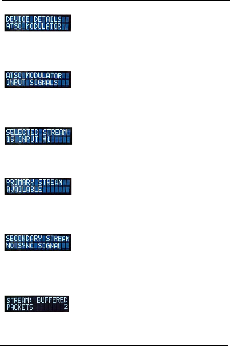
Innovator CHV0TD/RD-1 through CHV4TD/RD ATSC
Transmitter/Regenerative Translator w/DM8C Modulator Interface Description
Instruction Manual, Rev. 1 37
Figure 11.2: Device Details - ATSC Modulator Select
Menu Level ATSC Details Top Level
Description
This screen provides access to the read only parameters of
the ATSC modulator.
Parameter Range N/A
Figure 11.2.1: Device Details - Input Signals Category
Menu Level ATSC Details / Input Signals Top Level
Description
This screen provides access to read only input signal
parameters of the ATSC modulator.
Parameter Range N/A
Figure 11.2.1.1: Device Details - Input Signals - Selected Stream
Menu Level ATSC Details / Input Signals / Selected Stream
Description This screen indicates which input path is currently selected.
Parameter Range Input #1 or Input #2
Figure 11.2.1.2: Device Details - Input Signals - Primary Stream Status
Menu Level ATSC Details / Input Signals / Primary Stream
Description
This menu indicates if the allocated primary stream is
available or not.
Parameter Range "Available" or "No Sync Signal"
Figure 11.2.1.3: Device Details - Input Signals - Secondary Stream Status
Menu Level ATSC Details / Input Signals / Secondary Stream
Description
This menu indicates if the secondary stream is available or
not.
Parameter Range "Available" or "No Sync Signal"
Figure 11.2.1.4: Device Details - Input Signals - Stream: Number of Buffered
Packets
Menu Level ATSC Details / Input Signals / Stream Buffered Packet Count
Description
This display indicates how many packets are stored in the
input buffer.
Parameter Range Minimum of 0
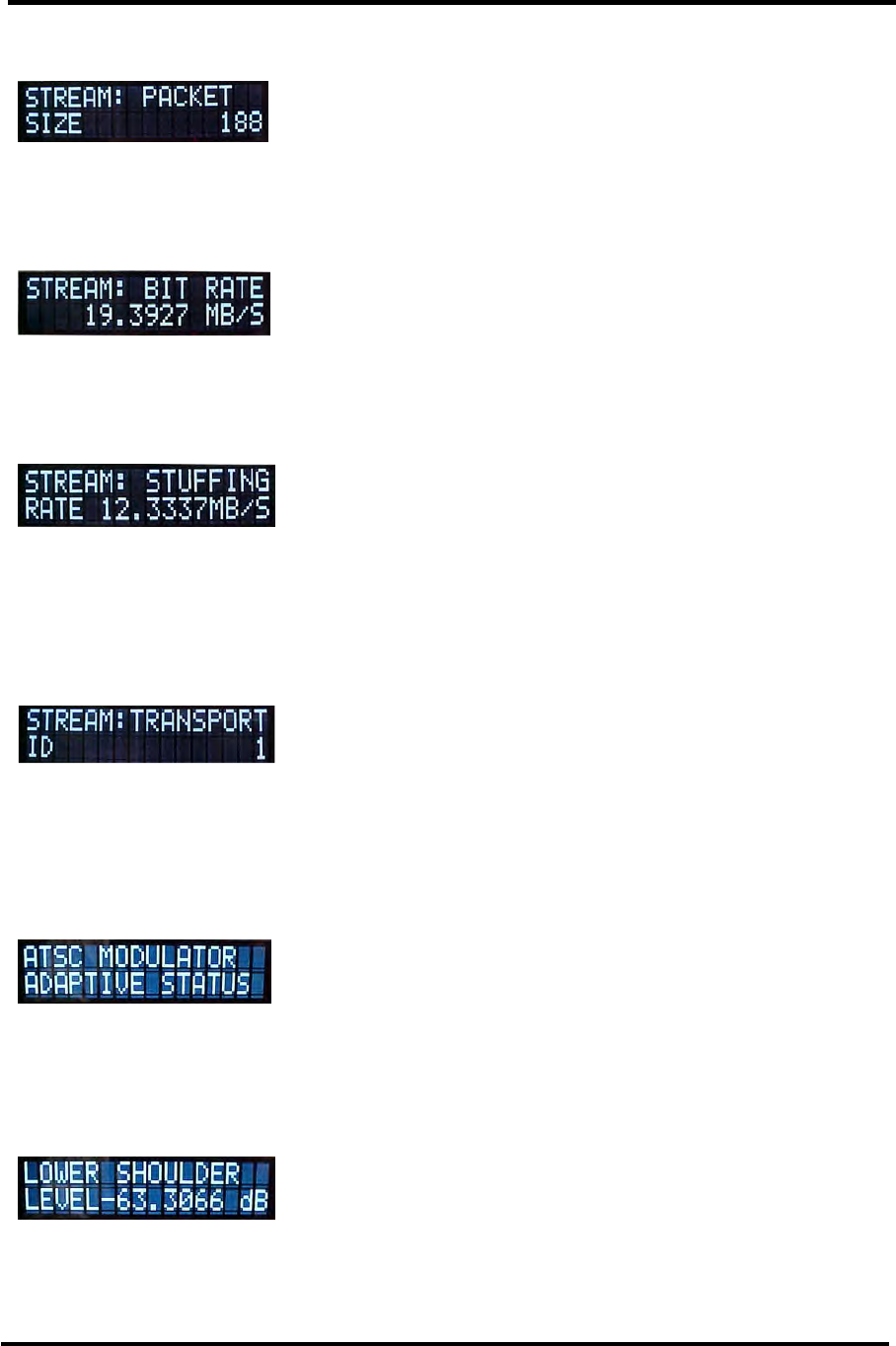
Innovator CHV0TD/RD-1 through CHV4TD/RD ATSC
Transmitter/Regenerative Translator w/DM8C Modulator Interface Description
Instruction Manual, Rev. 1 38
Figure 11.2.1.5: Device Details - Input Signals - Stream: Packet Size
Menu Level ATSC Details / Input Signals / Primary Stream Packet Size
Description This display indicates the transport stream packet size.
Parameter Range 188 or 204
Figure 11.2.1.6: Device Details - Input Signals - Stream: Bit Rate
Menu Level ATSC Details / Input Signals / Stream Bit Rate
Description This is the detected bit rate of the input transport stream.
Parameter Range
Figure 11.2.1.7: Device Details - Input Signals - Stream: Stuffing Rate
Menu
Level ATSC Details / Input Signals / Stream Stuffing Rate
Description
This is the detected stuffing rate of the input transport stream.
Parameter
Range
Figure 11.2.1.8: Device Details - Input Signals - Stream: TS ID
Menu
Level ATSC Details / Input Signals / Stream TS ID Value
Description
This is the detected TS ID value of the input stream.
Parameter
Range 0 to 65535
Figure 11.2.2: Device Details - Adaptive Precorrection Status Category
Menu Level ATSC Details / Adaptive Status Top Level
Description
This screen provides access to read only adaptive system
parameters.
Parameter Range N/A
Figure 11.2.2.1: Device Details - Adaptive Signals - Upper Shoulder Level
Menu Level ATSC Details / Adaptive Signals / Lower Shoulder Value
Description
When valid, this is the measured level in dB for the lower
shoulder.
Parameter Range 'Invalid' or measured level in dB

Innovator CHV0TD/RD-1 through CHV4TD/RD ATSC
Transmitter/Regenerative Translator w/DM8C Modulator Interface Description
Instruction Manual, Rev. 1 39
Figure 11.2.2.2: Device Details - Adaptive Signals - Upper Shoulder Level
Menu Level ATSC Details / Adaptive Signals / Upper Shoulder Value
Description
When valid, this is the measured level in dB for the upper
shoulder.
Parameter Range 'Invalid' or measured level in dB
Figure 11.2.2.3: Device Details - Adaptive Signals - Amplitude Ripple
Menu Level ATSC Details / Adaptive Signals / Amplitude Ripple Value
Description
When valid, this is the measured level in dB for the amplitude
ripple.
Parameter Range 'Invalid' or measured level in dB.
Figure 11.2.2.4: Device Details - Adaptive Signals - Group Delay
Menu Level ATSC Details / Adaptive Signals / Group Delay Value
Description When valid, this is the measured group delay in nano seconds.
Parameter Range 'Invalid' or measured level in nS.
Figure 11.2.2.5: Device Details - Adaptive Signals - Nonlinear Sample
Menu Level ATSC Details / Adaptive Signals / Nonlinear Sample Level
Description
When valid, this is the RF sample level used for nonlinear
precorrection.
Parameter Range
'Invalid' or measured level in dB. Required level for
precorrection is 0 dBm +/- 10 dB.
Figure 11.2.2.6: Device Details - Adaptive Signals - Nonlinear Correction Operational
Mode
Menu Level ATSC Details / Adaptive Signals / Nonlinear Adjust Mode
Description
Nonlinear Precorrection can be enabled or disabled through read
/ write parameters. This value tells us the operational status of
nonlinear precorrection.
Parameter Range
"Auto Applying", "Not Running", "Monitoring", "Initializing" or
"Initializing xx" where xx is the percentage of completion.
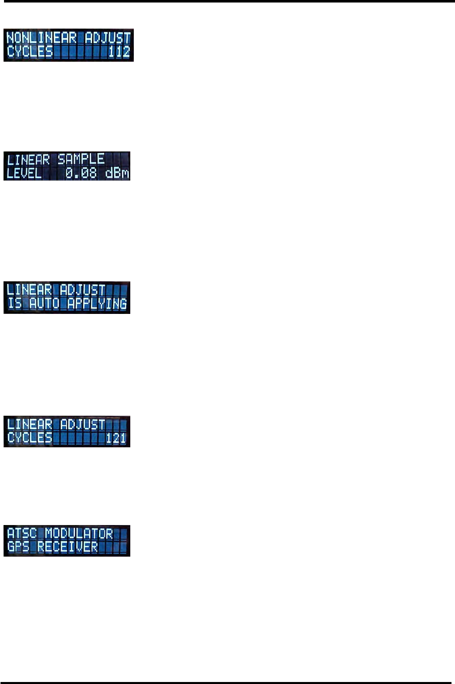
Innovator CHV0TD/RD-1 through CHV4TD/RD ATSC
Transmitter/Regenerative Translator w/DM8C Modulator Interface Description
Instruction Manual, Rev. 1 40
Figure 11.2.2.7: Device Details - Adaptive Signals - Nonlinear Correction Cycle Count
Menu Level ATSC Details / Adaptive Signals / Nonlinear Cycle Count
Description
This value is a count of the number of times nonlinear
precorrection has been updated since corrector reset or
modulator reboot.
Parameter Range
Figure 11.2.2.8: Device Details - Adaptive Signals - Linear Sample
Menu Level ATSC Details / Adaptive Signals / Linear Sample Level
Description
When valid, this is the RF sample level used for linear
precorrection.
Parameter Range
'Invalid' or measured level in dB. Required level for precorrection
is 0 dBm +/- 10 dB.
Figure 11.2.2.9: Device Details - Adaptive Signals - Linear Correction Operational
Mode
Menu Level ATSC Details / Adaptive Signals / Linear Adjust Mode
Description
Linear Precorrection can be enabled or disabled through read /
write parameters. This value tells us the operational status of
linear precorrection.
Parameter Range
"Auto Applying", "Not Running", "Monitoring", "Initializing" or
"Initializing xx" where xx is the percentage of completion.
Figure 11.2.2.10: Device Details - Adaptive Signals - Linear Correction Cycle Count
Menu Level ATSC Details / Adaptive Signals / Linear Cycle Count
Description
This value is a count of the number of times linear precorrection
has been updated since corrector reset or modulator reboot.
Parameter Range
Figure 11.2.3: Device Details - GPS Category (Only present if GPS Option is present)
Menu Level ATSC Details / GPS Status Top Level
Description
This screen provides access to read only GPS system parameters
if this optional component is present.
Parameter Range N/A
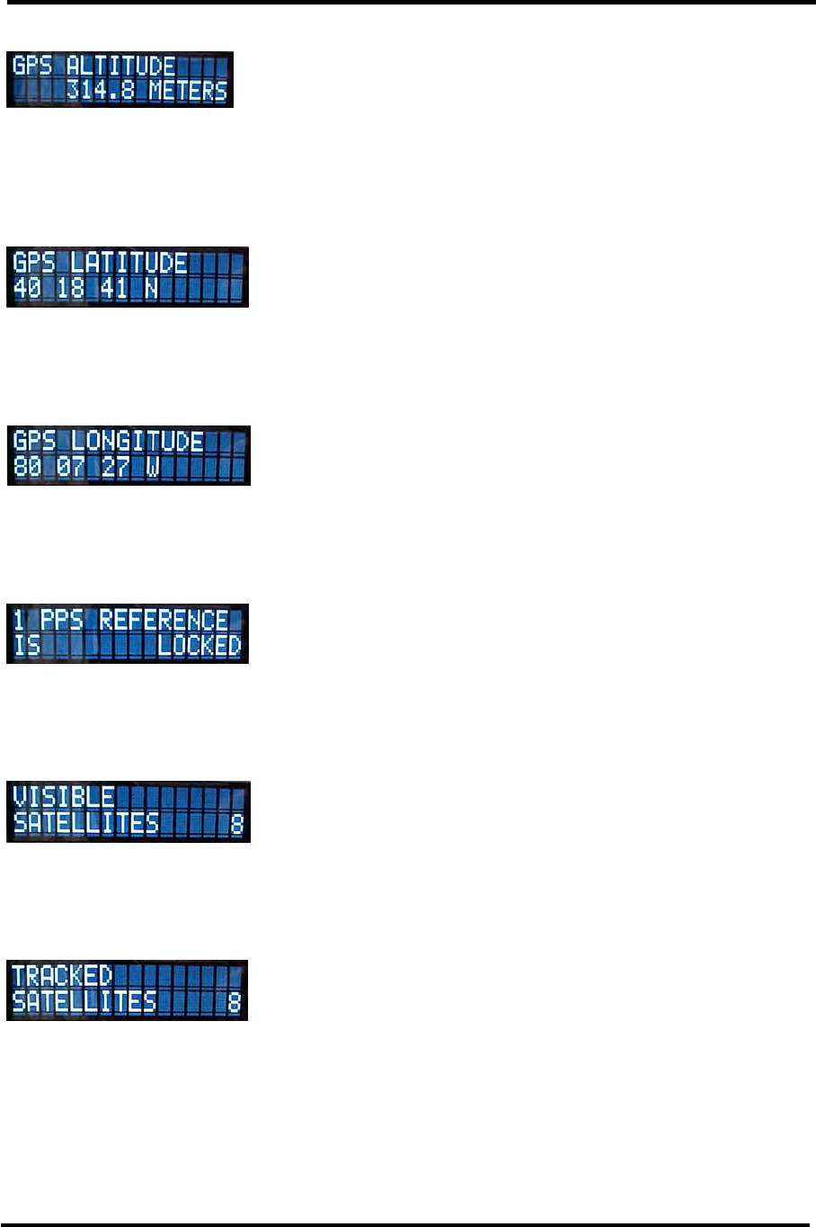
Innovator CHV0TD/RD-1 through CHV4TD/RD ATSC
Transmitter/Regenerative Translator w/DM8C Modulator Interface Description
Instruction Manual, Rev. 1 41
Figure 11.2.3.1: Device Details - GPS - Altitude
Menu Level ATSC Details / GPS Status / Altitude
Description
This is the current altitude in meters as measured by the GPS
receiver.
Parameter Range N/A
Figure 11.2.3.2: Device Details - GPS - Latitude
Menu Level ATSC Details / GPS Status / Latitude
Description This is the current latitude in DD MM SS N/S format.
Parameter Range N/A
Figure 11.2.3.3: Device Details - GPS - Longitude
Menu Level ATSC Details / GPS Status / Longitude
Description This is the current longitude in DD MM SS E/W format.
Parameter Range N/A
Figure 11.2.3.4: Device Details - GPS - 1 PPS Reference Signal Status
Menu Level ATSC Details / GPS Status / 1 PPS Status
Description This screen tells us if the 1PPS output is locked.
Parameter Range "Locked" or "Unlocked"
Figure 11.2.3.5: Device Details - GPS - Visible Satellites
Menu Level ATSC Details / GPS Status / Visible Satellites
Description This screen indicated the number of satellites that are visible.
Parameter Range Minimum of 0
Figure 11.2.3.6: Device Details - GPS - Tracked Satellites
Menu Level ATSC Details / GPS Status / Tracked Satellites
Description
This screen indicated the number of satellites used to generate
references, date and time.
Parameter Range Minimum of 0
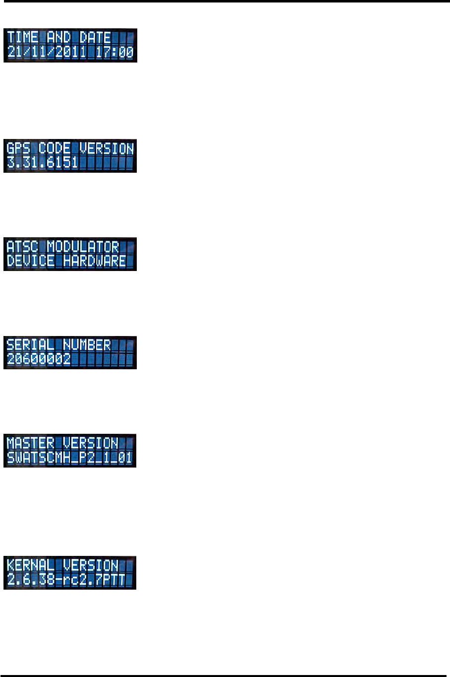
Innovator CHV0TD/RD-1 through CHV4TD/RD ATSC
Transmitter/Regenerative Translator w/DM8C Modulator Interface Description
Instruction Manual, Rev. 1 42
Figure 11.2.3.7: Device Details - GPS - Date and Time
Menu Level ATSC Details / GPS Status / Date and Time
Description
This is the date and time of the GPS based on satellites and time
zone.
Parameter Range N/A
Figure 11.2.3.8: Device Details - GPS - Firmware Version
Menu Level ATSC Details / GPS Status / Firmware Version
Description This screen indicates the firmware version of the GPS system.
Parameter Range N/A
Figure 11.2.4: Device Details - Device Hardware Category
Menu Level ATSC Details / Device Hardware Top Level
Description This screen provides access to read only hardware parameters.
Parameter Range N/A
Figure 11.2.4.1: Device Details - Hardware - Serial Number
Menu Level ATSC Details / Device Hardware / Serial Number
Description This is the serial number of the modulator assembly.
Parameter Range N/A
Figure 11.2.4.2: Device Details - Hardware - Master Version
Menu Level ATSC Details / Device Hardware / Master Version
Description
This is character string identifies the master version of firmware
installed. This value is longer than 16 characters so the value is
scrolled across the display.
Parameter Range N/A
Figure 11.2.4.3: Device Details - Hardware - Kernal Version
Menu Level ATSC Details / Device Hardware / Kernal Version
Description This is character string identifies the embedded Kernal version.
Parameter Range N/A
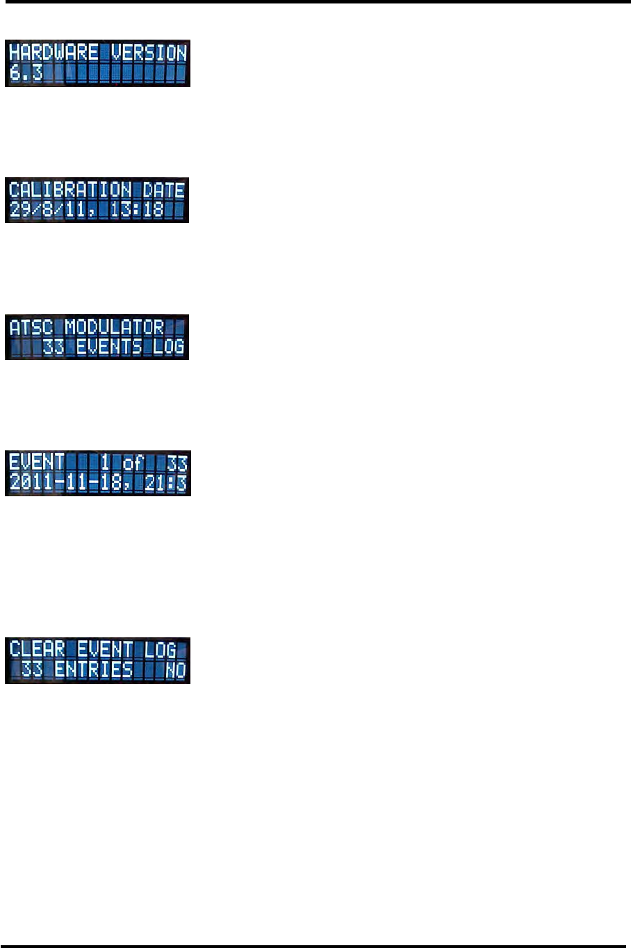
Innovator CHV0TD/RD-1 through CHV4TD/RD ATSC
Transmitter/Regenerative Translator w/DM8C Modulator Interface Description
Instruction Manual, Rev. 1 43
Figure 11.2.4.4: Device Details - Hardware - Hardware Version
Menu Level ATSC Details / Device Hardware / Hardware Version
Description This is character string identifies the board's hardware version.
Parameter Range N/A
Figure 11.2.4.5: Device Details - Hardware - Calibration Date
Menu Level ATSC Details / Device Hardware / Calibration Date
Description This is character string identifies the modulators calibration date.
Parameter Range N/A
Figure 11.2.5: Device Details - Event Log List Category
Menu Level ATSC Details / Event Log Top Level
Description This screen provides access to read or clear the event log.
Parameter Range N/A
Figure 11.2.5.1: Device Details - Event Log View
Menu Level ATSC Details / Event Log View
Description
This screen provides access to read specific events. The date
and time of the event are indicated then the specific event
details. Since this information is longer than 16 characters, the
text is scrolled across the screen.
Parameter Range N/A
Figure 11.2.5.2: Device Details - Event Log Clear
Menu Level ATSC Details / Event Log Clear
Description This screen provides access to clear all events of the log.
Parameter Range "Yes" or "No"
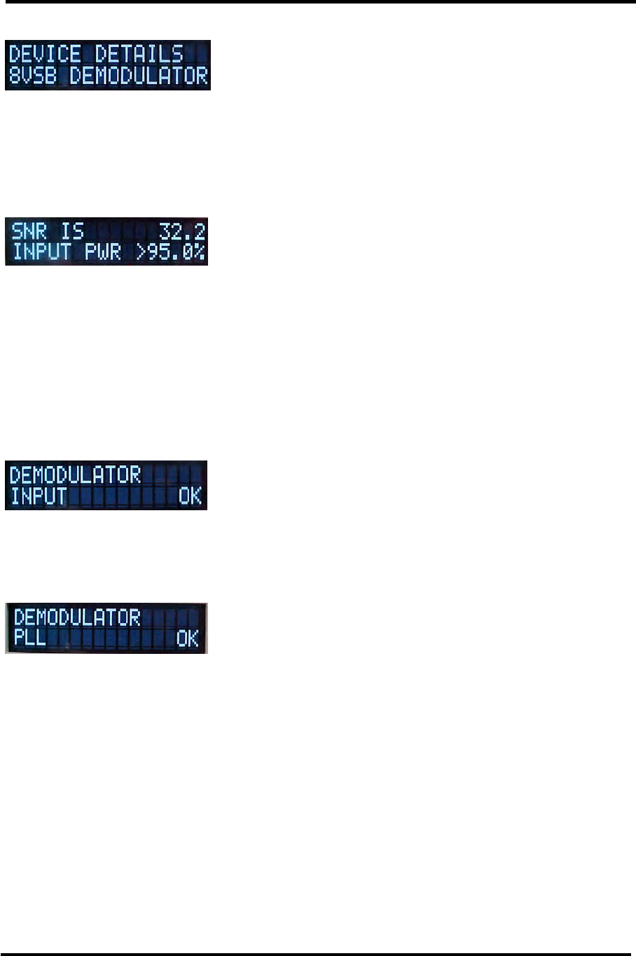
Innovator CHV0TD/RD-1 through CHV4TD/RD ATSC
Transmitter/Regenerative Translator w/DM8C Modulator Interface Description
Instruction Manual, Rev. 1 44
Figure 11.3: Translator 8VSB Demodulator Details Screen (RD)
Menu Level
System Device Details \ 8VSB Demodulator Details Main Sub
Screen
Description Push the ENTER button to access the Device 8VSB Demodulator
submenus or push the DOWN Arrow to view the next main menu,
which is the Device Details 8VSB Modulator Main Sub Menu.
Figure 11.3.1: System Input Details Screen (RD)
Menu Level 8VSB Demodulator Details Sub Screen
Description This screen provides the user information on the signal to noise
ratio and signal strength of the received signal. The signal to
noise ratio is provided on this menu to indicate to the user the
quality of the receive signal. This reading also assists the user in
the positioning of the antenna. The signal strength ranges from
0 to 100% and typically should be above 40% for reliable
operation. The signal strength allows the user to optimize the
position of the receive antenna.
Figure 11.3.2: Demodulator Details Screen (RD)
Menu Level 8VSB Demodulator Details Sub Screen
Description This menu indicates whether there is a signal present at the
demodulator.
Figure 11.3.3: Demodulator Phase Lock Loop Details Screen (RD)
Menu Level 8VSB Demodulator Details Sub Screen
Description This menu indicates whether the Phase Lock Loop is locked in the
demodulator.
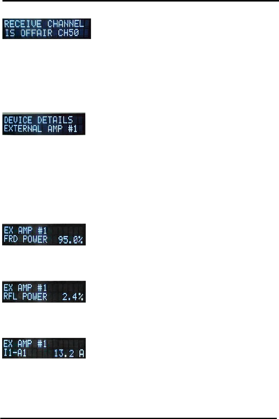
Innovator CHV0TD/RD-1 through CHV4TD/RD ATSC
Transmitter/Regenerative Translator w/DM8C Modulator Interface Description
Instruction Manual, Rev. 1 45
Figure 11.3.4: Receiver Input Channel Details Screen (RD)
Menu Level 8VSB Demodulator Details Sub Screen
Description This menu indicates the input channel to the Demodulator
circuit.
Pushing the Left Arrow will display the System Device Details
8VSB Demodulator Values Main Sub Screen and then pushing the
Down arrow will access the System Device Details 8VSB
Modulator Main Sub Screens.
Figure 11.4: External Amplifier Device Details Screen (TD/RD)
Menu Level Device Details External Amplifier #1 Details Main Screen
Description This is the Transmitter Device Details External Amplifier Main
Sub Screen. This is the final Device Details Main Sub Menu.
Push the ENTER button to access the Device External Amplifier
#1. Push the LEFT Arrow to go back the Main Device Details
Screen. Then push the DOWN Arrow to access the Transmitter
Set Up Main Menu.
NOTE: Shown below are the External Amplifier #1 Details Screens. The External
Amplifier #2, #3 or #4 Details Screens are presented in the same order if they are
present in the system.
Figure 11.4.1: External Amplifier #1 Forward Power Details Screen (TD/RD)
Menu Level Device Details External Amplifier #1 Details Sub Screen
Description Indicates Output Power for external amplifier #1.
NOTE: See the final test data sheet for the typical value.
Figure 11.4.2: External Amplifier #1 Reflected Power Details Screen (TD/RD)
Menu Level Device Details External Amplifier #1 Details Sub Screen
Description Indicates Reflected Power for external amplifier #1.
NOTE: See the final test data sheet for the typical value.
Figure 11.4.3: External Amplifier #1 I1-A1 Current Details Screen (TD/RD)
Menu Level Device Details External Amplifier #1 Details Sub Screen
Description Indicates Current of the A1 device in the external amplifier #1.
NOTE: See the final test data sheet for the typical current value.
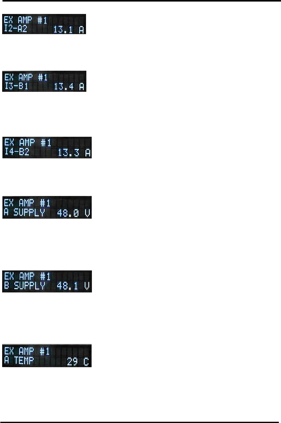
Innovator CHV0TD/RD-1 through CHV4TD/RD ATSC
Transmitter/Regenerative Translator w/DM8C Modulator Interface Description
Instruction Manual, Rev. 1 46
Figure 11.4.4: External Amplifier #1 I2-A2 Current Details Screen (TD/RD)
Menu Level Device Details External Amplifier #1 Details Sub Screen
Description Indicates Current of the A2 device in the external amplifier #1.
NOTE: See the final test data sheet for the typical current value.
Figure 11.4.5: External Amplifier #1 I3-B1 Current Details Screen (TD/RD)
Menu Level Device Details External Amplifier #1 Details Sub Screen
Description Indicates Current of the B1 device in the external amplifier #1.
NOTE: See the final test data sheet for the typical current value.
Figure 11.4.6: External Amplifier #1 I4-B2 Current Details Screen (TD/RD)
Menu Level Device Details External Amplifier #1 Details Sub Screen
Description Indicates Current of the B2 device in the external amplifier #1.
NOTE: See the final test data sheet for the typical current value.
Figure 11.4.7: External Amplifier #1 A Power Supply Details Screen (TD/RD)
Menu Level Device Details External Amplifier #1 Details Sub Screen
Description Indicates the voltage of the A power supply in the external
amplifier #1.
NOTE: Typical voltage value is +42VDC or +48VDC w/888A
devices.
Figure 11.4.8: External Amplifier #1 B Power Supply Details Screen (TD/RD)
Menu Level Device Details External Amplifier #1 Details Sub Screen
Description Indicates the voltage of the B power supply in the external
amplifier #1.
NOTE: Typical voltage value is +42VDC or +48VDC w/888A
devices.
Figure 11.4.9: External Amplifier #1 A Temperature Details Screen (TD/RD)
Menu Level Device Details External Amplifier #1 Details Sub Screen
Description Indicates the temperature of the A heatsink in the external
amplifier #1. NOTE: Typical temperature for DVB = ≈20-30°C
above ambient.
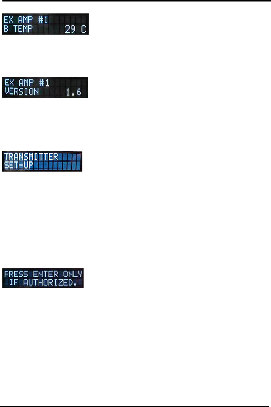
Innovator CHV0TD/RD-1 through CHV4TD/RD ATSC
Transmitter/Regenerative Translator w/DM8C Modulator Interface Description
Instruction Manual, Rev. 1 47
Figure 11.4.10: External Amplifier #1 B Temperature Details Screen (TD/RD)
Menu Level Device Details External Amplifier #1 Details Sub Screen
Description Indicates the temperature of the B heatsink in the external
amplifier #1. NOTE: Typical temperature for DVB = ≈20-30°C
above ambient.
Figure 11.4.11: External Amplifier #1 Code Version Details Screen (TD/RD)
Menu Level Device Details External Amplifier #1 Details Sub Screen
Description Indicates the code version in the external amplifier #1.
Device Setup Screens - These are read / write parameters.
Figure 12: Setup (TD/RD)
Menu Level Main Setup Menu
Description This screen provides access to all transmitter read / write
parameters. This is the System Set Up Main Screen. Push the
ENTER button to access the Authorization Warning Main Sub
Screen or since this is the final Main Screen, pushing the DOWN
Arrow will take you back to the System RF Power Default Screen.
The Set Up item or parameter that can be changed on the displayed sub menu
screen, is indicated by pushing the ENTER button, which causes the changeable item
to blink. The UP or DOWN arrow will change the selection until the desired result is
displayed. Pushing the ENTER Button will accept the change.
Figure 12A: Authorized Personnel Screen (TD/RD)
Menu Level Setup Authorized Screen
Description This screen of the system notifies an operator that they are only
to proceed if they are authorized to make changes to the
system's operation. Changes made within the following set-up
screens can affect the system’s output power level, output
frequency, and the general behavior of the system. Please do
not make changes within the system's set-up screens unless you
are familiar with the operation of the system. Pressing the ENTER
button will display the Enter Key Sets to Change screen.

Innovator CHV0TD/RD-1 through CHV4TD/RD ATSC
Transmitter/Regenerative Translator w/DM8C Modulator Interface Description
Instruction Manual, Rev. 1 48
Figure 12B: Right or Enter Key Sets to Change Mode Screen (TD/RD)
Menu Level Setup Right Key Sets Change Mode Screen
Description This screen informs the operator that to make changes, the Enter
key or the Right key must be pushed, which will cause the
display that can be changed to blink. Use the up or down key to
change the display and the left or right key to move the blinking
item on the display. After changes are made in the Set Up
Menus pushing the enter Key, Button, will accept the changes
made. With the Right Key Sets To Change Mode screen
displayed, pushing the ENTER button will access the first main
submenu under the Set Up main menu, which is the Chassis
Values Set Up Menu.
Figure 12.1: Chassis Values Main Set Up Screen (TD/RD)
Menu Level Setup Menus Chassis Values Main Sub Screen
Description Push the ENTER button to access the Chassis Values submenus
or push the DOWN Arrow to view the next Set Up Main Sub
Screen, which is the Set Up ATSC Modulator Main Sub Screen.
NOTE: Refer to the description in Figure 12B for how to change
the values on the following set-up screens.
Figure 12.1.1: Chassis Values Forward Power Set Up Screen (TD/RD)
Menu Level Setup Menus Chassis Values Sub Screen
Description Remote or front panel adjustment of the output power of the
transmitter. The bar graph indicates the range remaining in the
adjustment.
NOTE: If the transmitter's output power is being adjusted
through the web page, the transmitter's forward power will be
blinking on this screen. It will remain blinking while the
transmitter is adjusting to the desired target power level.
Figure 12.1.2: Chassis Values Model Number Set Up Screen (TD/RD)
Menu Level Setup Menus Chassis Values Sub Screen
Description This screen allows the set up of the Model Number of the
transmitter/regenerative translator. This causes the system to
access the proper parameters to be displayed on the LCD
screens.
NOTE: Do not change this screen without first consulting with
Axcera.
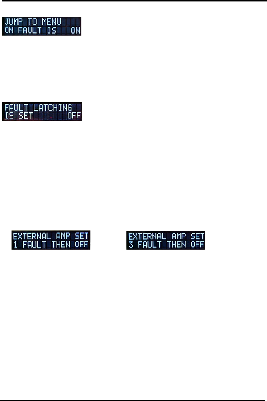
Innovator CHV0TD/RD-1 through CHV4TD/RD ATSC
Transmitter/Regenerative Translator w/DM8C Modulator Interface Description
Instruction Manual, Rev. 1 49
Figure 12.1.3: Chassis Values Jump to Menu on Fault Set Up Screen (TD/RD)
Menu Level Setup Menus Chassis Values Sub Screen
Description The 'Jump To Menu' setting screen allows an operator to change
how the transmitter's display system works. When this value is
set 'ON' and a new fault occurs, the transmitter will automatically
change the display screen to show the new fault condition.
When this value is set 'OFF', the display screen does not change
when a new fault is detected.
Figure 12.1.4: Chassis Values Latch On an Input Fault Set Up Screen (TD/RD)
Menu Level Setup Menus Chassis Values Sub Screen
Description This screen, by selecting ON, allows the user to select that the
system will latch the fault if it occurs, then if the problem is
corrected the fault will still register. Since latched faults are
used to set the status LED color, when fault latching is OFF, the
status LED should only be green if there are no faults or red if
there are one or more active faults. When fault latching is ON,
the status LED will be amber if there are no current faults but a
fault was previously detected and is now a latched fault. A
blinking amber status LED indicates that there are no current
faults or latched faults but that an internal signal source is
selected instead of an external sourced.
Figure 12.1.5: Chassis Values External Amplifier Fault Number Set Up Screen
(TD/RD)
1. 2.
Menu Level Setup Menus Chassis Values Sub Screen
Description This screen allows the user to set the number of faults that are
allowed before the external amplifier is disabled. NOTE: Only
used with external amplifiers are in the system.
Screen 1: If One Fault is selected and a fault occurs in an
external amplifier, the entire transmitter is muted and the
faulted external amplifier is latched off. The transmitter is then
unmuted and any external amplifiers (fully or partially
operational) are enabled.
Screen 2: If Three Fault is selected and a fault occurs in an
external amplifier, the entire transmitter is muted and unmuted
three times before the faulted external amplifier is latched off.
NOTE: Faulted amplifier sections are re-enabled when latched
faults are cleared in the event log. See Figure 10.1 for more
information on clearing the logs.
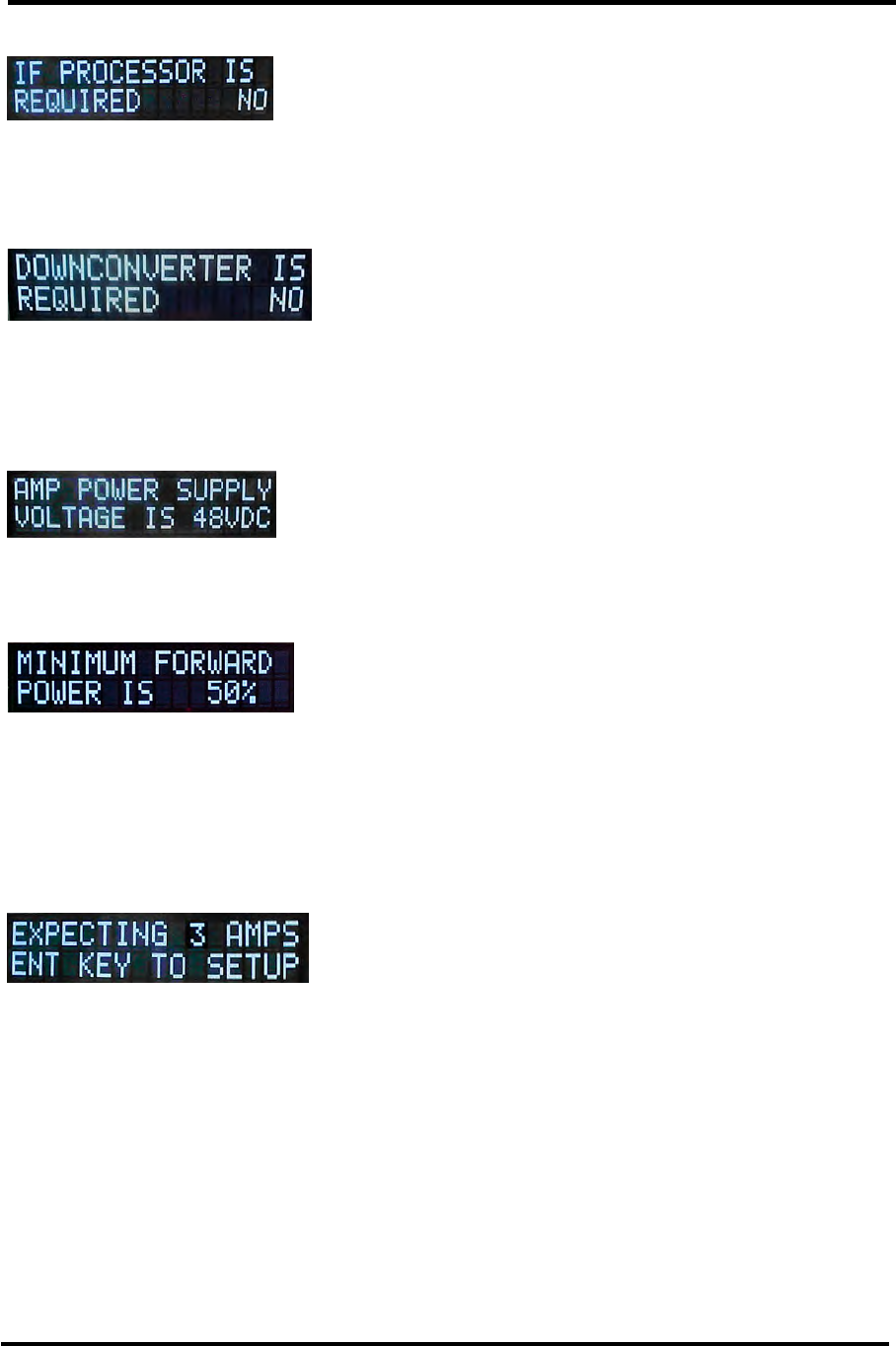
Innovator CHV0TD/RD-1 through CHV4TD/RD ATSC
Transmitter/Regenerative Translator w/DM8C Modulator Interface Description
Instruction Manual, Rev. 1 50
Figure 12.1.6: Chassis Values IF Processor Selection Set Up Screen (TD/RD)
Menu Level Setup Menus Chassis Values Sub Screen
Description This screen allows the user to select that the system has an IF
Processor.
Figure 12.1.7: Chassis Values Downconverter Selection Set Up Screen (TD/RD)
Menu Level Setup Menus Chassis Values Sub Screen
Description This screen allows the user to select that the system has a
Downconverter.
Figure 12.1.8: Chassis Values Amplifier Power Supply Voltage Set Up Screen
(TD/RD)
Menu Level Setup Menus Chassis Values Sub Screen
Description This screen allows the user to select the Power Supply Voltage.
Figure 12.1.9: Chassis Values Forward Power Fault Adjust Set Up Screen (TD/RD)
Menu Level Setup Menus Chassis Values Sub Screen
Description This screen allows the operator to configure a forward power
fault threshold setting. When the exciter is enabled for at least a
few seconds and the system forward power is not greater than or
equal to this setting, a fault is indicated on the status LED and
also on the remote fault indicator pin.
Figure 12.1.10: Chassis Values Number of Amplifiers in System Screen (TD/RD)
Menu Level Setup Menus Chassis Values Sub Screen
Description This screen indicates the number of external amplifier drawers in
the system. By selecting the enter key, the system will scan to
find the number of external amplifier drawers. NOTE: Do not
change this screen without first consulting with Axcera.
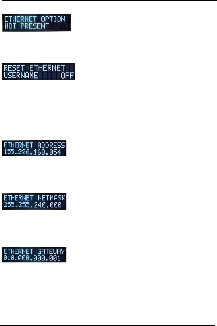
Innovator CHV0TD/RD-1 through CHV4TD/RD ATSC
Transmitter/Regenerative Translator w/DM8C Modulator Interface Description
Instruction Manual, Rev. 1 51
Figure 12.1.11: Chassis Values Ethernet Option Set Up Screen (TD/RD)
Menu Level Setup Menus Chassis Values Sub Screen
Description Only displayed if Ethernet Controller is not present in your
system.
Figure 12.1.12: Chassis Values Ethernet User Name Set Up Screen (TD/RD)
Menu Level Setup Menus Chassis Values Sub Screen
Description When the optional Ethernet Controller is present, this screen is
displayed. It is used to reset the first username / password
account of the Ethernet controller. There are a total a five
accounts available on the Web. If this operation is selected, ON,
and the change accepted, only the fist username / password
account file is replaced, with the user name set to ‘admin’ and
the password set to ‘axcera’.
Figure 12.1.13: Chassis Values Ethernet Address Set Up Screen (TD/RD)
Menu Level Setup Menus Chassis Values Sub Screen
Description When the optional Ethernet Controller module is present, this
screen is used to view or change the Ethernet TCP Address of the
controller.
Figure 12.1.14: Chassis Values Ethernet Netmask Set Up Screen (TD/RD)
Menu Level Setup Menus Chassis Values Sub Screen
Description When the optional Ethernet Controller module is present, this
screen is used to view or change the TCP subnet mask of the
Ethernet controller.
Figure 12.1.15: Chassis Values Ethernet Gateway Set Up Screen (TD/RD)
Menu Level Setup Menus Chassis Values Sub Screen
Description When the optional Ethernet Controller module is present, this
screen is used to view or change the TCP gateway (router)
address of the Ethernet controller.
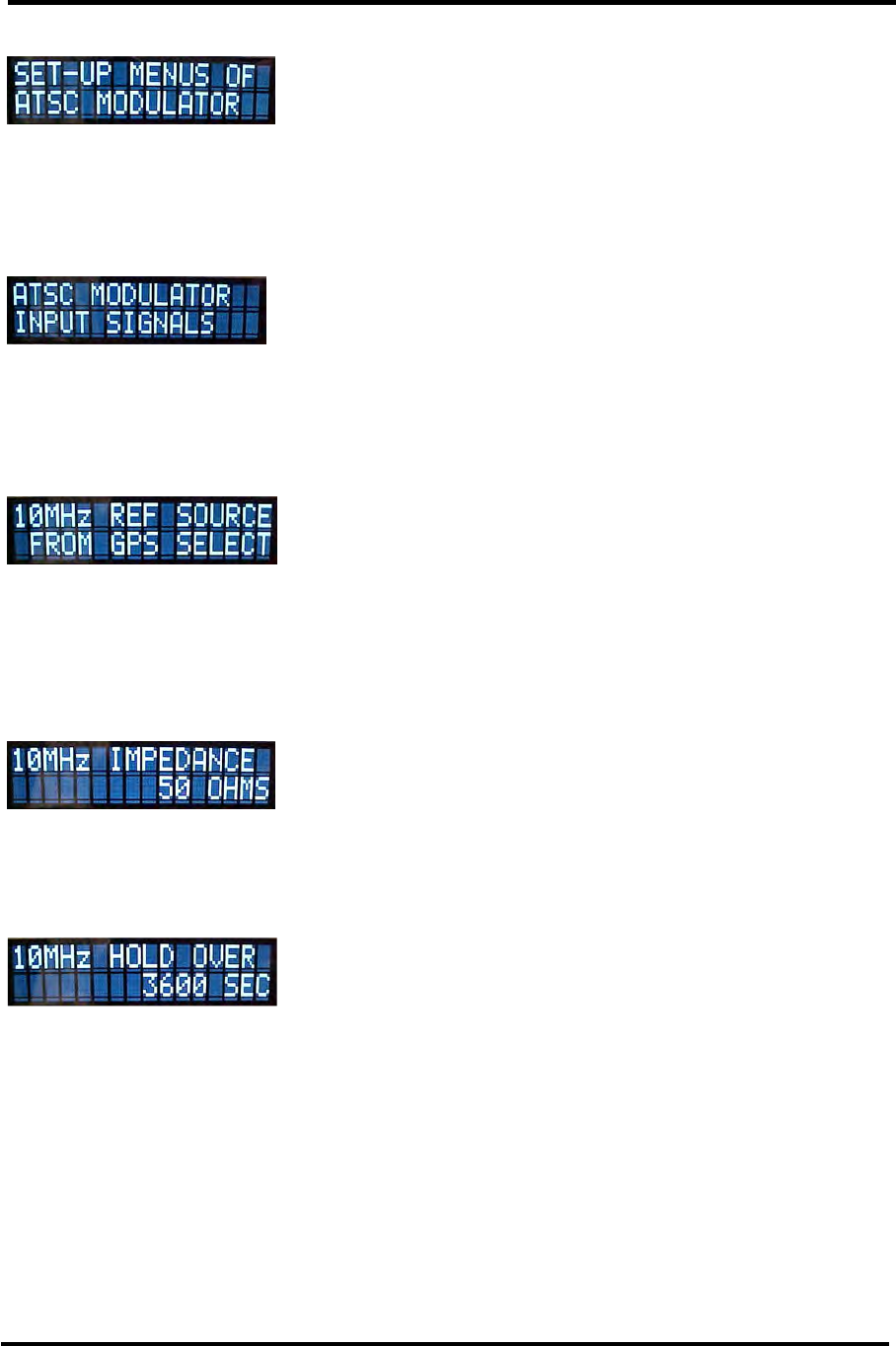
Innovator CHV0TD/RD-1 through CHV4TD/RD ATSC
Transmitter/Regenerative Translator w/DM8C Modulator Interface Description
Instruction Manual, Rev. 1 52
Figure 12.2: Device Setup - ATSC Modulator Select
Menu Level ATSC Modulator Setup Top Level
Description
This screen provides access to the modulator's read / write
parameters.
Parameter Range N/A
Figure 12.2.1: Device Setup - Input Signals Category
Menu Level ATSC Setup / Input Signals Top Level
Description
This screen provides access to read / write input signal
parameters.
Parameter Range N/A
Figure 12.2.2: Device Setup - Input Signals - 10MHz Reference Source
Menu Level ATSC Setup / Inputs Signals / 10MHz Reference Source
Description
Used to report or set the primary 10MHz reference source. When
"GPS" or "External" are selected, "Internal" is automatically used
if the selected source is not operational.
Parameter Range "Auto Select", "GPS", "External", or "Internal"
Figure 12.2.3: Device Setup - Input Signals - 10MHz Reference Impedance
Menu Level ATSC Setup / Inputs Signals / 10MHz Reference Impedance
Description This is the 10MHz reference source impedance.
Parameter Range "50 Ohms", or "High Impedance"
Figure 12.2.4: Device Setup - Input Signals - 10MHz Reference Holdover
Menu Level ATSC Setup / Inputs Signals / 10MHz Reference Holdover
Description
This value specifies the minimum duration of 10MHz reference
loss required for raising the 10MHz reference alarm.
Parameter Range 0 to 3600 seconds
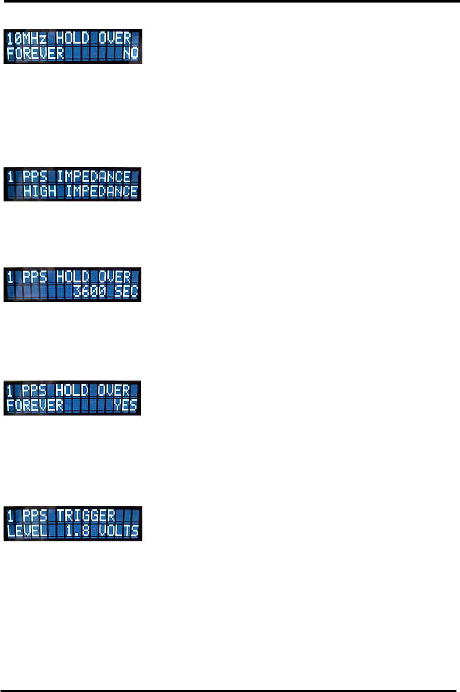
Innovator CHV0TD/RD-1 through CHV4TD/RD ATSC
Transmitter/Regenerative Translator w/DM8C Modulator Interface Description
Instruction Manual, Rev. 1 53
Figure 12.2.5: Device Setup - Input Signals - 10MHz Reference Holdover Forever
Menu Level
ATSC Setup / Inputs Signals / 10MHz Reference Holdover
Forever
Description
When set to "Yes" the 10MHz reference loss alarm is disabled
and the back-up reference is used whenever an external
reference is lost.
Parameter Range "Yes" or "No"
Figure12.2.6: Device Setup - Input Signals - 1 PPS Impedance
Menu Level ATSC Setup / Inputs Signals / 1 PPS Impedance
Description This is the 1 PPS reference source impedance.
Parameter Range "50 Ohms", or "High Impedance"
Figure 12.2.7: Device Setup - Input Signals - 1 PPS Holdover
Menu Level ATSC Setup / Inputs Signals / 1 PPS Holdover
Description
This value specifies the minimum duration of 1 PPS reference
loss required for raising the 1 PPS reference alarm.
Parameter Range 0 to 3600 seconds
Figure 12.2.8: Device Setup - Input Signals - 1 PPS Holdover Forever
Menu Level ATSC Setup / Inputs Signals / 1 PPS Holdover Forever
Description
When set to "Yes" the 1 PPS reference loss alarm is disabled and
the internal synthesized 1 PPS reference is used whenever an
external reference is lost.
Parameter Range "Yes" or "No"
Figure 12.2.9: Device Setup - Input Signals - 1 PPS Trigger Level
Menu Level ATSC Setup / Inputs Signals / 1 PPS Trigger Level
Description
This value is the trigger level for the 1 PPS external input in
volts.
Parameter Range 0 to 3.5 volts

Innovator CHV0TD/RD-1 through CHV4TD/RD ATSC
Transmitter/Regenerative Translator w/DM8C Modulator Interface Description
Instruction Manual, Rev. 1 54
Figure 12.2.10: Device Setup - Input Signals - 1 PPS Trigger Edge
Menu Level ATSC Setup / Inputs Signals / 1 PPS Trigger Edge
Description This is the trigger edge of the 1 PPS external input.
Parameter Range "Rising" or "Falling"
Figure 12.2.11: Device Setup - Input Signals - Input Stream 1 Format
Menu Level ATSC Setup / Inputs Signals / Input Stream 1 Format
Description This screen specifies the stream format of physical input 1.
Parameter Range "ASI" or "SMPTE310M"
Figure 12.2.12: Device Setup - Input Signals - Input Stream 2 Format
Menu Level ATSC Setup / Inputs Signals / Input Stream 2 Format
Description This screen specifies the stream format of physical input 2.
Parameter Range "ASI" or "SMPTE310M"
Figure 12.2.13: Device Setup - Input Signals - Primary Stream
Menu Level ATSC Setup / Inputs Signals / Primary Stream
Description Used to select the primary transport stream.
Parameter Range "Input 1" or "Input 2"
Figure 12.2.14: Device Setup - Input Signals - Secondary Stream
Menu Level ATSC Setup / Inputs Signals / Secondary Stream
Description Used to select the secondary transport stream.
Parameter Range "Input 1" or "Input 2"
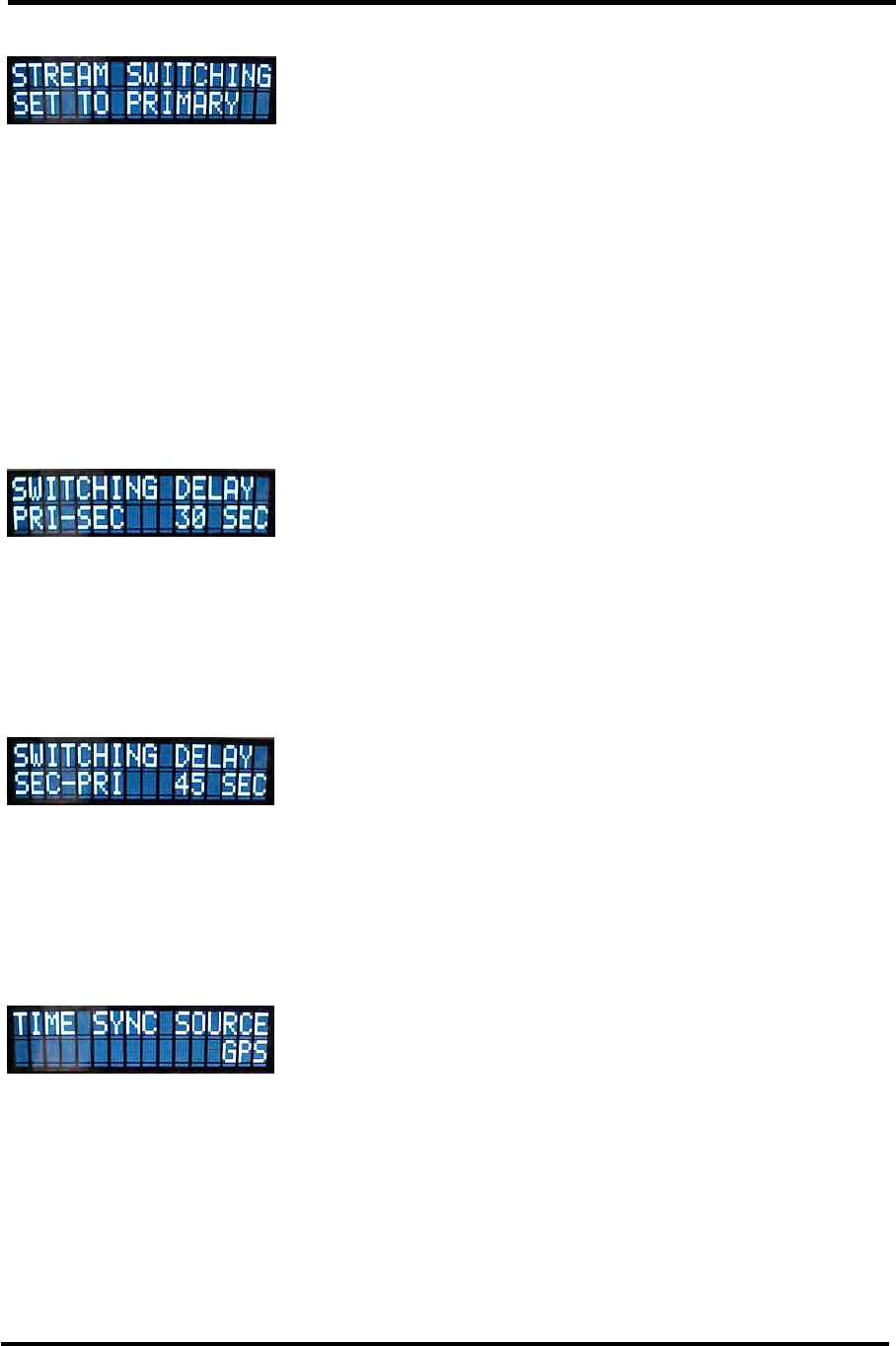
Innovator CHV0TD/RD-1 through CHV4TD/RD ATSC
Transmitter/Regenerative Translator w/DM8C Modulator Interface Description
Instruction Manual, Rev. 1 55
Figure 12.2.15: Device Setup - Input Signals - Stream Switching
Menu Level ATSC Setup / Inputs Signals / Stream Switching
Description
This screen is used to configure the stream switching system.
"Set To Primary" is used to fix the selected stream to the Primary
Input source. "Set To Secondary" is used to fix the selected
stream to the Secondary Input source. "Prefer Primary" is used
to select the primary stream if it is present or switch to the
secondary stream if the primary stream is not present. "Use
Either Input" is used to switch to the other stream if the selected
stream is not present but not to switch back if the other stream
returns.
Parameter Range
"Set To Primary", "Set To Secondary", "Prefer Primary", or
"Use Either Input"
Figure 12.2.16: Device Setup - Input Signals - Primary To Secondary Switching Delay
Menu Level
ATSC Setup / Inputs Signals / Primary To Secondary Switching
Delay
Description
This value sets the switching delay from primary source to
secondary source after an error is detected in the primary
transport stream.
Parameter Range 0 to 300 seconds
Figure 12.2.17: Device Setup - Input Signals - Secondary To Primary Switching Delay
Menu Level
ATSC Setup / Inputs Signals / Secondary To Primary Switching
Delay
Description
This value sets the switching delay from secondary source to
primary source after an error is detected in the secondary
transport stream.
Parameter Range 0 to 300 seconds
Figure 12.2.18: Device Setup - Input Signals - Time Sync Source
Menu Level ATSC Setup / Inputs Signals / Time Sync Source
Description
This value sets the preferred source for time and date
information.
Parameter Range "GPS", "Manual", "NTP"
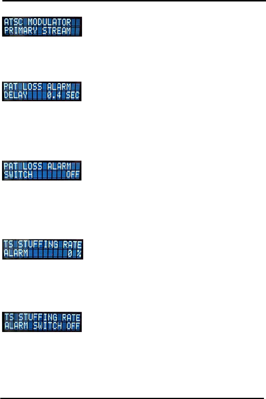
Innovator CHV0TD/RD-1 through CHV4TD/RD ATSC
Transmitter/Regenerative Translator w/DM8C Modulator Interface Description
Instruction Manual, Rev. 1 56
Figure 12.2.19: Device Setup - Primary Stream Category
Menu Level ATSC Setup / Primary Stream Top Level
Description
This screen provides access to read / write primary stream
parameters.
Parameter Range N/A
Figure 12.2.20: Device Setup - Primary Stream - PAT Loss Alarm Delay
Menu Level ATSC Setup / Primary Stream / PAT Loss Alarm Delay
Description
This value sets the delay time before reporting of a PAT Loss
alarm. An alarm is activated if the PAT table in not detected in
the primary transport stream at least once per specified time
interval.
Parameter Range 0 to 10.0 seconds
Figure 12.2.21: Device Setup - Primary Stream - PAT Loss Alarm Switch
Menu Level ATSC Setup / Primary Stream / PAT Loss Alarm Switch Control
Description
This value determines if loss of PAT table input shall activate the
automatic switch over to the secondary transport stream source
based on the current stream switching configuration.
Parameter Range "On" or "Off"
Figure 12.2.22: Device Setup - Primary Stream - Transport Stream Stuffing Rate
Alarm
Menu Level
ATSC Setup / Primary Stream / Transport Stream Stuffing Rate
Alarm
Description
This value determines the level were too many MPEG-2 null
packets generate an alarm.
Parameter Range 0 to 100%
Figure 12.2.23: Device Setup - Primary Stream - TS Stuffing Rate Alarm Switch
Menu Level
ATSC Setup / Primary Stream / TS Stuffing Rate Alarm Switch
Control
Description
This value determines if a Transport Stream Stuffing Rate Alarm
shall activate the automatic switch over to the secondary
transport stream source based on the current stream switching
configuration.
Parameter Range "On" or "Off"
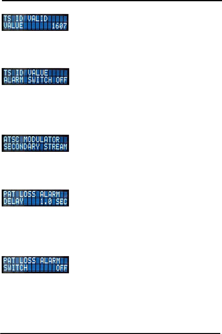
Innovator CHV0TD/RD-1 through CHV4TD/RD ATSC
Transmitter/Regenerative Translator w/DM8C Modulator Interface Description
Instruction Manual, Rev. 1 57
Figure 12.2.24: Device Setup - Primary Stream - Transport Stream ID Valid Value
Menu Level ATSC Setup / Primary Stream / Transport Stream ID Valid Value
Description This value sets the expected transport stream ID value.
Parameter Range 0 to 100%
Figure 12.2.25: Device Setup - Primary Stream - Transport Stream ID Value Alarm
Switch
Menu Level ATSC Setup / Primary Stream / TS ID Alarm Switch Control
Description
This value determines if a Transport Stream ID Value mismatch
shall activate the automatic switch over to the secondary
transport stream source based on the current stream switching
configuration.
Parameter Range "On" or "Off"
Figure 12.2.26: Device Setup - Secondary Stream Category
Menu Level ATSC Setup / Secondary Stream Top Level
Description
This screen provides access to read / write secondary stream
parameters.
Parameter Range N/A
Figure 12.2.27: Device Setup - Secondary Signals - PAT Loss Alarm Delay
Menu Level ATSC Setup / Secondary Stream / PAT Loss Alarm Delay
Description
This value sets the delay time before reporting of a PAT Loss
alarm. An alarm is activated if the PAT table in not detected in
the primary transport stream at least once per specified time
interval.
Parameter Range 0 to 10.0 seconds
Figure 12.2.28: Device Setup - Secondary Stream - PAT Loss Alarm Switch
Menu Level ATSC Setup / Secondary Stream / PAT Loss Alarm Switch Control
Description
This value determines if loss of PAT table input shall activate the
automatic switch over to the primary transport stream source
based on the current stream switching configuration.
Parameter Range "On" or "Off"
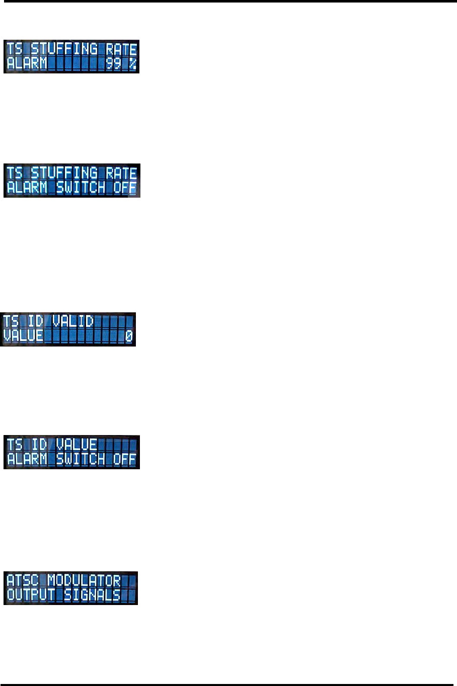
Innovator CHV0TD/RD-1 through CHV4TD/RD ATSC
Transmitter/Regenerative Translator w/DM8C Modulator Interface Description
Instruction Manual, Rev. 1 58
Figure 12.2.29: Device Setup - Secondary Stream - Transport Stream Stuffing Rate
Alarm
Menu Level
ATSC Setup / Secondary Stream / Transport Stream Stuffing
Rate Alarm
Description
This value determines the level were too many MPEG-2 null
packets generate an alarm.
Parameter Range 0 to 100%
Figure 12.2.30: Device Setup - Secondary Stream - TS Stuffing Rate Alarm Switch
Menu Level
ATSC Setup / Secondary Stream / TS Stuffing Rate Alarm Switch
Control
Description
This value determines if a Transport Stream Stuffing Rate Alarm
shall activate the automatic switch over to the primary transport
stream source based on the current stream switching
configuration.
Parameter Range "On" or "Off"
Figure 12.2.31: Device Setup - Secondary Stream - Transport Stream ID Valid Value
Menu Level
ATSC Setup / Secondary Stream / Transport Stream ID Valid
Value
Description This value sets the expected transport stream ID value.
Parameter Range 0 to 100%
Figure 12.2.32: Device Setup - Secondary Stream - Transport Stream ID Value Alarm
Switch
Menu Level ATSC Setup / Secondary Stream / TS ID Alarm Switch Control
Description
This value determines if a Transport Stream ID Value mismatch
shall activate the automatic switch over to the primary transport
stream source based on the current stream switching
configuration.
Parameter Range "On" or "Off"
Figure 12.2.33: Device Setup - Output Signals Category
Menu Level ATSC Setup / Output Signals Top Level
Description
This screen provides access to read / write output signal
parameters.
Parameter Range N/A
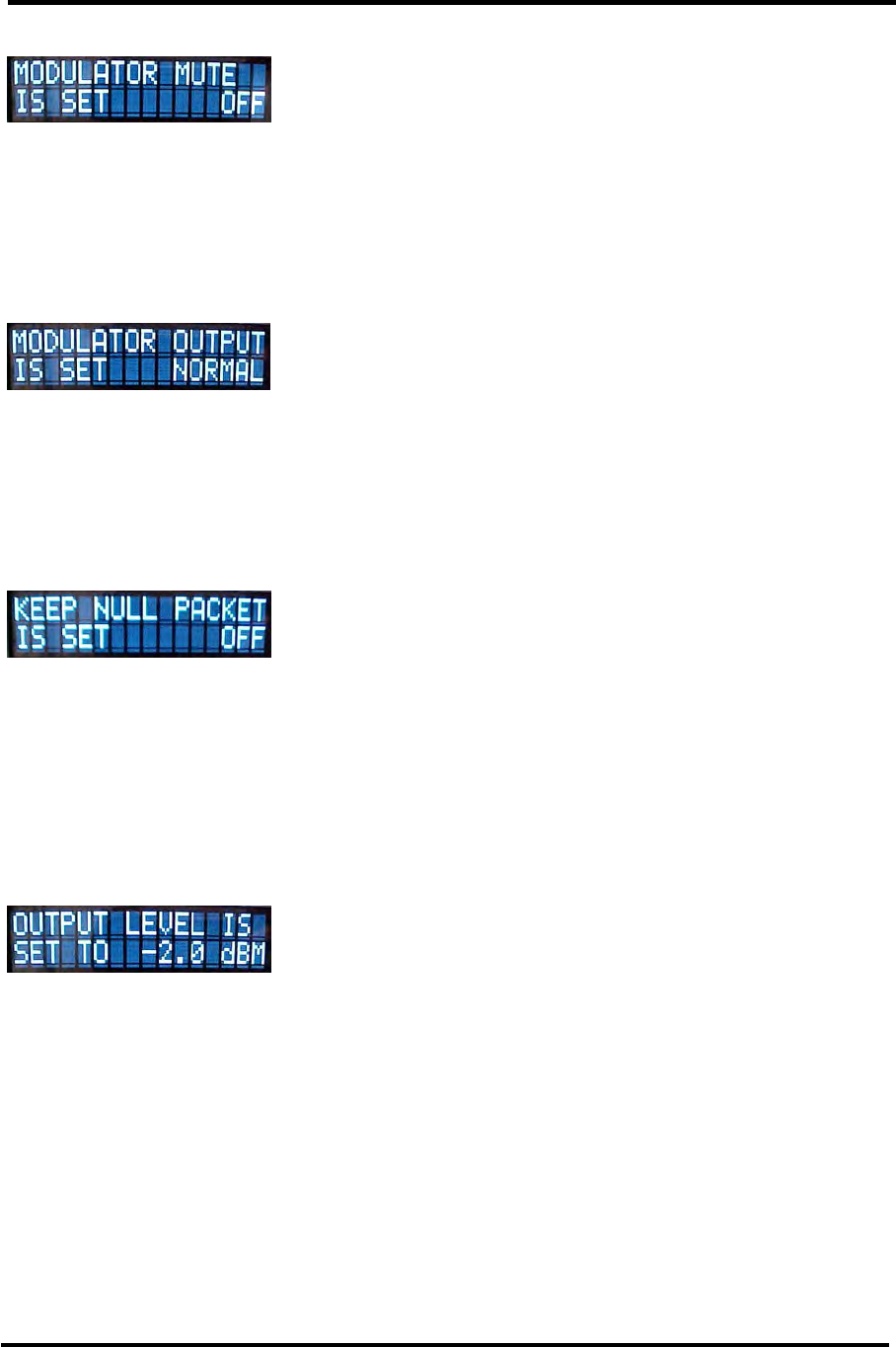
Innovator CHV0TD/RD-1 through CHV4TD/RD ATSC
Transmitter/Regenerative Translator w/DM8C Modulator Interface Description
Instruction Manual, Rev. 1 59
Figure 12.2.34: Device Setup - Output Signals - Modulator Mute
Menu Level ATSC Setup / Output Signals / Modulator Mute
Description
This value determines if the modulator's output if muted or
allowed to operate. When set to "On", the output is muted.
When set to "Off" the output is enabled but it may still be muted
due to other conditions.
Parameter Range "On" or "Off"
Figure 12.2.35: Device Setup - Output Signals - Modulator Output
Menu Level ATSC Setup / Output Signals / Modulator Output Mode
Description
This value determines the RF output level. When set to
"Normal", the RF output level is normal but when set to
"Standby" the output level is reduced by -10dB relative to
normal. See also Figure 12.2.35.
Parameter Range "Normal" or "Standby"
Figure 12.2.36: Device Setup - Output Signals - Null Packet Usage
Menu Level ATSC Setup / Output Signals / Null Packet Usage
Description
Keep null packet "On" provides the most transparent transport
stream processing but "Off" provides the highest level of
flexibility with regards to gross input data rate (payload +
stuffing). Note: Payload + stuffing may exceed the nominal data
rate but payload data rate must not exceed the nominal data
rate.
Parameter Range "On" or "Off"
Figure 12.2.37: Device Setup - Output Signals - Output Level Set
Menu Level ATSC Setup / Output Signals / Output Level Set
Description
This value is used to set the current output level in dB relative to
the nominal level. Note: When modulator output mode is set to
standby, the output level is set to -10dB. See also Figure 12.2.35.
Parameter Range -10.0 to 0.0 dB

Innovator CHV0TD/RD-1 through CHV4TD/RD ATSC
Transmitter/Regenerative Translator w/DM8C Modulator Interface Description
Instruction Manual, Rev. 1 60
Figure 12.2.38: Device Setup - Output Signals - Output Frequency Set
Menu Level ATSC Setup / Output Signals / Output Frequency Set
Description
This value is used to set the output frequency in Hz. Each
position of frequency value may be individually set provided the
value is adjusted within the acceptable range.
Parameter Range 30,000,000 to 1,000,000,000 Hz
Figure 12.2.39: Device Setup - Output Signals - Output Frequency Offset
Menu Level ATSC Setup / Output Signals / Output Frequency Offset
Description
This value is used to apply an output frequency offset. Each
position is individually set provided the value is adjusted within
the acceptable range.
Parameter Range -8,388,608 to 8,388,607 Hz
Figure 12.2.40: Device Setup - Output Signals - Output Polarity
Menu Level ATSC Setup / Output Signals / Output Polarity
Description
This value is used to adjust the polarity of the output signal
spectrum. When set to "Normal", the lowest carrier number is
placed on the lowest spectrum frequency. When set to
"Inverted", the highest carrier number is placed on the lowest
spectrum frequency.
Parameter Range "Normal" or "Inverted"
Figure 12.2.41: Device Setup - Output Signals - Peak Clipping Level
Menu Level ATSC Setup / Output Signals / Peak Clipping Level
Description
This value is used to adjust the peak clipping level relative to the
average RMS at baseband.
Parameter Range 12.0 to 2.0 dB in 0.5 dB intervals. Typical value: 5 or 6dB
Figure 12.2.42: Device Setup - Output Signals - Peak Clipping Strength
Menu Level ATSC Setup / Output Signals / Peak Clipping Strength
Description
This value is used to adjust strength of applied peak clipping. '0'
equals hard clipping while '100' equals the maximum softness
(minimum sideband noise).
Parameter Range 0 to 100 %. Typical value is 50%
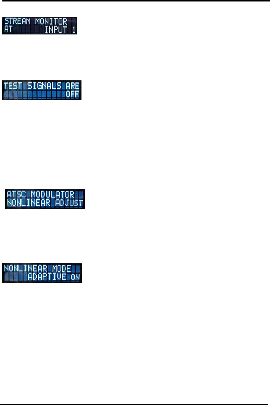
Innovator CHV0TD/RD-1 through CHV4TD/RD ATSC
Transmitter/Regenerative Translator w/DM8C Modulator Interface Description
Instruction Manual, Rev. 1 61
Figure 12.2.43: Device Setup - Output Signals - Stream Monitoring Location
Menu Level ATSC Setup / Output Signals / Stream Monitoring
Description
This value is used to determine the transport stream monitoring
location for the ASI Monitor Output port.
Parameter Range "Input 1", "Input 2", or "Output Stream"
Figure 12.2.44: Device Setup - Output Signals - Test Signals
Menu Level ATSC Setup / Output Signals / Test Signals
Description
This value is used to determine the status of the test signal
system. "Off" is the normal state where no test signals are
applied. "Single Carrier" enables a single carrier test signal.
"PRBS ON" is used to enable a forced transmission of stuffing
data (null packets) only. "PRBS Auto" is used to enable a
transmission of stuffing data (null packets) only when the input
stream is not available. "Test Signal" is used to enable a test
signal with a 3dB peak-to-average peak ratio.
Parameter Range "Off", "Single Carrier", "PRBS ON", "PRBS Auto", or "Test Signal"
Figure 12.2.45: Device Setup - Nonlinear Precorrector Adjustments Category
Menu Level ATSC Setup / Nonlinear Precorrector Adjustment Top Level
Description
This screen provides access to read / write parameters of the
Nonlinear Precorrector system.
Parameter
Range N/A
Figure 12.2.46: Device Setup - Nonlinear Adjust - Mode
Menu Level ATSC Setup / Nonlinear Adjust / Mode
Description
This value sets the mode of the nonlinear precorrector system.
"Only Monitor" is selected when nonlinear correction is disabled
but it still allows shoulder performance to be monitored. "Static
Correction" is selected to enable manual nonlinear correction.
"Adaptive On" is used to enable adaptive precorrection.
Parameter Range "Only Monitor", "Static Correction", or "Adaptive On"
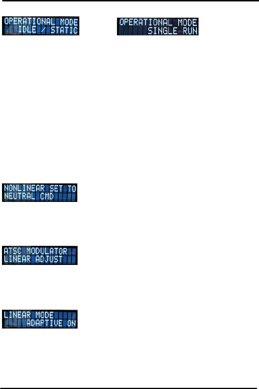
Innovator CHV0TD/RD-1 through CHV4TD/RD ATSC
Transmitter/Regenerative Translator w/DM8C Modulator Interface Description
Instruction Manual, Rev. 1 62
Figure 12.2.47: Device Setup - Nonlinear Adjust - Operational Mode
Menu Level ATSC Setup / Nonlinear Adjust / Operational Mode
Description
This value sets the operational mode of the nonlinear
precorrector system. "Idle / Static" is selected to apply current
correction characteristics but future changes are not
automatically made. "Single" is selected to have the system
calculate correction characteristics one time then system returns
to "Idle / Static". "Continuous" applies the current correction
characteristics and automatically monitors the system and
applies new correction values when better performance can be
obtained. "Run To Target" apples correction and applies new
correction values until the upper and lower spectrum shoulders
match target levels. "Automatic Run" is selected when
continuous precorrection is desired until the upper and lower
shoulder values are corrected. "Automatic Run" then holds
correction static with the option to have new correction values
automatically calculated and applied when output performance
subsequently drops below the set threshold.
Parameter Range
"Idle/Static", "Single", "Continuous", "Run To Target",
"Automatic Run"
Figure 12.2.48: Device Setup - Nonlinear Adjust - Reset To Neutral Command
Menu Level ATSC Setup / Nonlinear Adjust / Reset To Neutral Command
Description
This screen provides access to reset the nonlinear correction to
neutral.
Parameter Range "On" or "Off"
Figure 12.2.49: Device Setup - Linear Precorrector Adjustments Category
Menu Level ATSC Setup / Linear Precorrector Adjustment Top Level
Description
This screen provides access to read / write parameters of the
Linear Precorrector system.
Parameter Range N/A
Figure 12.2.50: Device Setup - Linear Adjust - Mode
Menu Level ATSC Setup / Linear Adjust / Mode
Description
This value sets the mode of the linear precorrector system.
"Only Monitor" is selected when linear correction is disabled but it
still allows group delay and amplitude ripple to be monitored.
"Static Correction" is selected to enable manual linear correction.
"Adaptive On" is used to enable adaptive precorrection.
Parameter Range "Only Monitor", "Static Correction", or "Adaptive On"
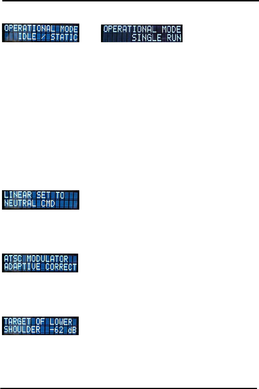
Innovator CHV0TD/RD-1 through CHV4TD/RD ATSC
Transmitter/Regenerative Translator w/DM8C Modulator Interface Description
Instruction Manual, Rev. 1 63
Figure 12.2.51: Device Setup - Linear Adjust - Operational Mode
Menu Level ATSC Setup / Linear Adjust / Operational Mode
Description
This value sets the operational mode of the linear precorrector
system. "Idle / Static" is selected to apply current correction
characteristics but future changes are not automatically made.
"Single" is selected to have the system calculate correction
characteristics one time then system returns to "Idle / Static".
"Continuous" applies the current correction characteristics and
automatically monitors the system and applies new correction
values when better performance can be obtained. "Run To
Target" apples correction and applies new correction values until
the upper and lower spectrum shoulders match target levels.
"Automatic Run" is selected when continuous precorrection is
desired until the upper and lower shoulder values are corrected.
"Automatic Run" then holds correction static with the option to
have new correction values automatically calculated and applied
when output performance subsequently drops below the set
threshold.
Parameter Range
"Idle/Static", "Single", "Continuous", "Run To Target", "Automatic
Run"
Figure 12.2.52: Device Setup - Linear Adjust - Reset To Neutral Command
Menu Level ATSC Setup / Linear Adjust / Reset To Neutral Command
Description
This screen provides access to reset the linear correction to
neutral.
Parameter Range "On" or "Off"
Figure 12.2.53: Device Setup - Adaptive Precorrector Adjustments Category
Menu Level ATSC Setup / Adaptive Precorrector Adjustment Top Level
Description
This screen provides access to read / write parameters of the
Adaptive Precorrector system.
Parameter Range N/A
Figure 12.2.54: Device Setup - Adaptive Precorrector - Lower Shoulder Target Value
Menu Level ATSC Setup / Adaptive Correct / Lower Shoulder Target Value
Description
This value can be is used by the adaptive precorrector systems
to start and stop linear and nonlinear precorrector operations.
This value specifically relates to the lower shoulder of the
feedback signal.
Parameter Range -60 to 0 dB

Innovator CHV0TD/RD-1 through CHV4TD/RD ATSC
Transmitter/Regenerative Translator w/DM8C Modulator Interface Description
Instruction Manual, Rev. 1 64
Figure 12.2.55: Device Setup - Adaptive Precorrector - Upper Shoulder Target Value
Menu Level ATSC Setup / Adaptive Correct / Upper Shoulder Target Value
Description
This value can be is used by the adaptive precorrector systems
to start and stop linear and nonlinear precorrector operations.
This value specifically relates to the upper shoulder of the
feedback signal.
Parameter Range -60 to 0 dB
Figure 12.2.56: Device Setup - Adaptive Precorrector - Amplitude Ripple Target
Value
Menu Level ATSC Setup / Adaptive Correct / Amplitude Ripple Target Value
Description
This value can be is used by the adaptive precorrector systems
to start and stop linear and nonlinear precorrector operations.
Parameter Range 0.0 to 5.0 dB
Figure 12.2.57: Device Setup - Adaptive Precorrector - Group Delay Target Value
Menu Level ATSC Setup / Adaptive Correct / Group Delay Target Value
Description
This value can be is used by the adaptive precorrector systems
to start and stop linear and nonlinear precorrector operations.
Parameter Range 0 to 1000 nS
Figure 12.2.58: Device Setup - Adaptive Precorrector - Lower Shoulder Hysteresis
Value
Menu Level
ATSC Setup / Adaptive Correct / Lower Shoulder Hysteresis
Value
Description
This value is used with the target value and the usage setting by
the adaptive precorrector systems to start and stop linear and
nonlinear precorrector operations.
Parameter Range 0 to 50 dB
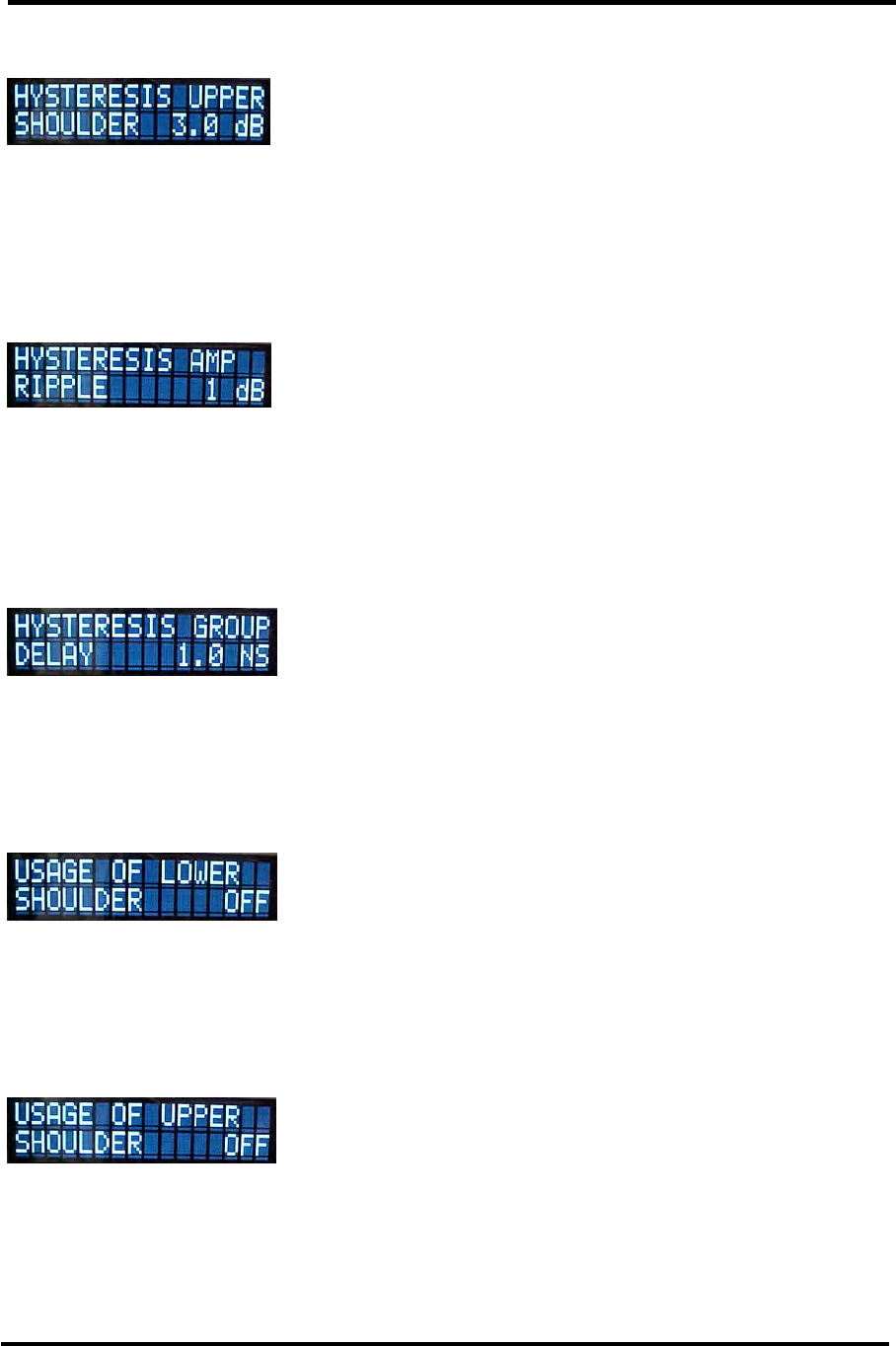
Innovator CHV0TD/RD-1 through CHV4TD/RD ATSC
Transmitter/Regenerative Translator w/DM8C Modulator Interface Description
Instruction Manual, Rev. 1 65
Figure 12.2.59: Device Setup - Adaptive Precorrector - Upper Shoulder Hysteresis
Value
Menu Level
ATSC Setup / Adaptive Correct / Upper Shoulder Hysteresis
Value
Description
This value is used with the target value and the usage setting by
the adaptive precorrector systems to start and stop linear and
nonlinear precorrector operations.
Parameter Range 0 to 50 dB
Figure 12.2.60: Device Setup - Adaptive Precorrector - Amplitude Ripple Hysteresis
Value
Menu Level
ATSC Setup / Adaptive Correct / Amplitude Ripple Hysteresis
Value
Description
This value is used with the target value and the usage setting by
the adaptive precorrector systems to start and stop linear and
nonlinear precorrector operations.
Parameter Range 0.00 to 5.00 dB
Figure 12.2.61: Device Setup - Adaptive Precorrector - Group Delay Hysteresis Value
Menu Level ATSC Setup / Adaptive Correct / Group Delay Hysteresis Value
Description
This value is used with the target value and the usage setting by
the adaptive precorrector systems to start and stop linear and
nonlinear precorrector operations.
Parameter Range 0 to 1000 nS
Figure 12.2.62: Device Setup - Adaptive Precorrector - Lower Shoulder Usage
Menu Level ATSC Setup / Adaptive Correct / Lower Shoulder Usage
Description
When set to "On", the target value and hysteresis value are used
by the adaptive precorrector systems to start and stop linear and
nonlinear precorrector operations.
Parameter Range "On", or "Off"
Figure 12.2.63: Device Setup - Adaptive Precorrector - Upper Shoulder Usage
Menu Level ATSC Setup / Adaptive Correct / Upper Shoulder Usage
Description
When set to "On", the target value and hysteresis value are used
by the adaptive precorrector systems to start and stop linear and
nonlinear precorrector operations.
Parameter Range "On", or "Off"
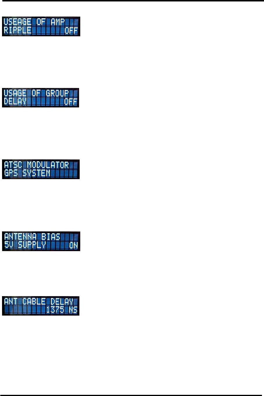
Innovator CHV0TD/RD-1 through CHV4TD/RD ATSC
Transmitter/Regenerative Translator w/DM8C Modulator Interface Description
Instruction Manual, Rev. 1 66
Figure 12.2.64: Device Setup - Adaptive Precorrector - Amplitude Ripple Usage
Menu Level ATSC Setup / Adaptive Correct / Amplitude Ripple Usage
Description
When set to "On", the target value and hysteresis value are used
by the adaptive precorrector systems to start and stop linear and
nonlinear precorrector operations.
Parameter Range "On", or "Off"
Figure 12.2.65: Device Setup - Adaptive Precorrector - Group Delay Usage
Menu Level ATSC Setup / Adaptive Correct / Group Delay Usage
Description
When set to "On", the target value and hysteresis value are used
by the adaptive precorrector systems to start and stop linear and
nonlinear precorrector operations.
Parameter Range "On", or "Off"
Figure 12.2.66: Device Setup - GPS System Category
Menu Level ATSC Setup / GPS System Top Level
Description
This screen provides access to read / write parameters of the
optional GPS system. Note: Not all systems have the GPS
system enabled.
Parameter Range N/A
Figure 12.2.67: Device Setup - GPS - Antenna Bias
Menu Level ATSC Setup / GPS / Antenna Bias
Description
When set to "On", the 5V antenna bias supply is enabled. When
set "Off", the antenna is not powered.
Parameter Range "On", or "Off"
Figure 12.2.68: Device Setup - GPS - Antenna Cable Delay
Menu Level ATSC Setup / GPS / Antenna Cable Delay
Description
This value is used to specify the cable delay associated with the
type and length of cable used to connect the antenna to the
modulator. This value is very important in SNF systems.
Parameter Range 0 to 1375 nS

Innovator CHV0TD/RD-1 through CHV4TD/RD ATSC
Transmitter/Regenerative Translator w/DM8C Modulator Interface Description
Instruction Manual, Rev. 1 67
Figure 12.2.69: Device Setup - GPS - Internal Reference Holdover Time
Menu Level ATSC Setup / GPS / Internal Reference Holdover Time
Description
This value is the holdover time for which it is acceptable to
continue operating on the internal TCXO reference of the GPS
whenever GPS lock is lost.
Parameter Range 0 to 3600 seconds
Figure 12.2.70: Device Setup - GPS - Internal Reference Holdover Forever
Menu Level ATSC Setup / GPS / Internal Reference Holdover Forever
Description
When set to "Yes", the modulator may continue indefinitely to
operate on the internal TCXO reference of the GPS whenever
GPS lock is lost. When set to "No", the modulator will raise a
GPS Unlocked alarm after the Internal Reference Holdover Time has
expired with possible output muting based on alarm configurations.
Parameter Range "On", or "Off"
Figure 12.2.71: Device Setup - General Device IO Category
Menu Level ATSC Setup / General Device IO Top Level
Description
This screen provides access to the general read / write
parameters system used for general communication with the
modulator.
Parameter Range N/A
Figure 12.2.72: Device Setup - General IO - Serial Baud Rate
Menu Level ATSC Setup / General IO / Serial Baud Rate
Description
This screen is used to view and change the serial baud rate. The
modulator must be communicating with the transmitter for
changes to be made and the transmitter automatically tries
different baud rates if it is not communicating with a modulator.
The default of 115200 works well therefore slower baud rates are
not recommended.
Parameter Range 115200, 57600, 38400, 19200, 9600, 4800, or 2400
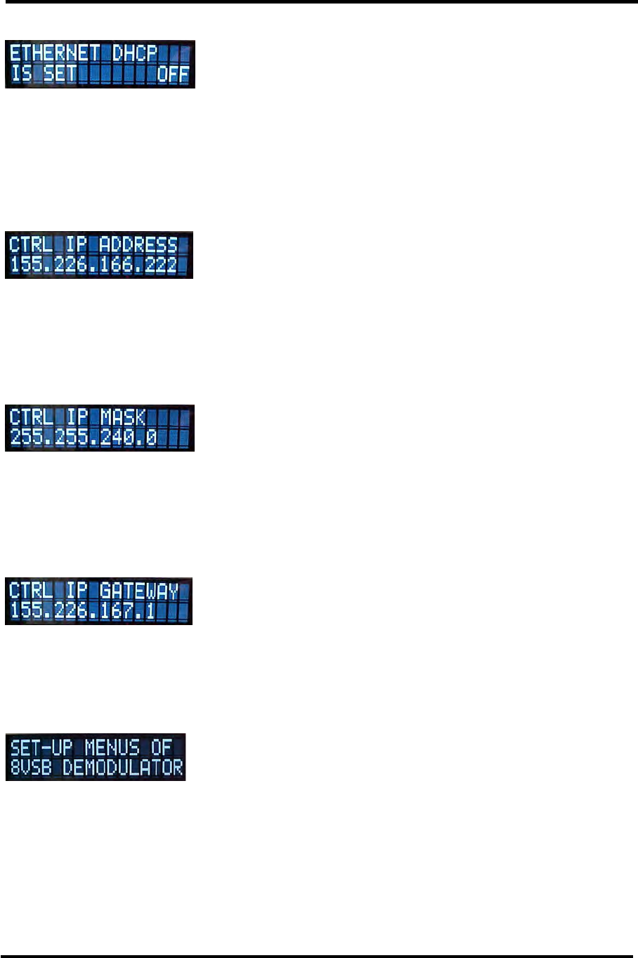
Innovator CHV0TD/RD-1 through CHV4TD/RD ATSC
Transmitter/Regenerative Translator w/DM8C Modulator Interface Description
Instruction Manual, Rev. 1 68
Figure 12.2.73: Device Setup - General IO - Ethernet DHCP
Menu Level ATSC Setup / General IO / Ethernet DHCP
Description
When set to "On", the modulator will attempt to get its TCP/IP
address from a DHCP server. DHCP set to "Off" is recommended
so that remote operators will not need to search and find the IP
address of the device.
Parameter Range "On", or "Off"
Figure 12.2.74: Device Setup - General IO - Ethernet IP Address
Menu Level ATSC Setup / General IO / Ethernet IP Address
Description
This screen displays the actual control IP address of the
modulator device. This is not the TsoIP address if Transport
Stream over IP is implemented.
Parameter Range IP values 0.0.0.0 thru 255.255.255.255
Figure 12.2.75: Device Setup - General IO - Ethernet IP Subnet Mask
Menu Level ATSC Setup / General IO / Ethernet IP subnet Mask
Description
This screen displays the actual control IP subnet mask of the
modulator device. This is not the TSoIP mask if Transport Stream
over IP is implemented.
Parameter Range IP values 0.0.0.0 thru 255.255.255.255
Figure 12.2.76: Device Setup - General IO - Ethernet IP Gateway
Menu Level ATSC Setup / General IO / Ethernet IP Gateway
Description
This screen displays the actual IP gateway of the modulator
device.
Parameter Range IP values 0.0.0.0 thru 255.255.255.255
Figure 12.3: Device Setup – 8VSB Demodulator
Menu Level 8VSB Demodulator Setup Main Screen
Description This is the System Set Up 8VSB Demodulator Main Sub Screen
that is only present in the Regenerative Translator mode. Push
the ENTER button to access the Set Up 8VSB Demodulator
submenus or push the DOWN Arrow to view the next Set Up
Main Sub Screen, which is the Set Up 8VSB Modulator Main Sub
Screen. NOTE: Refer to the description in Figure 12B for how to
change the values on the following set-up screens.
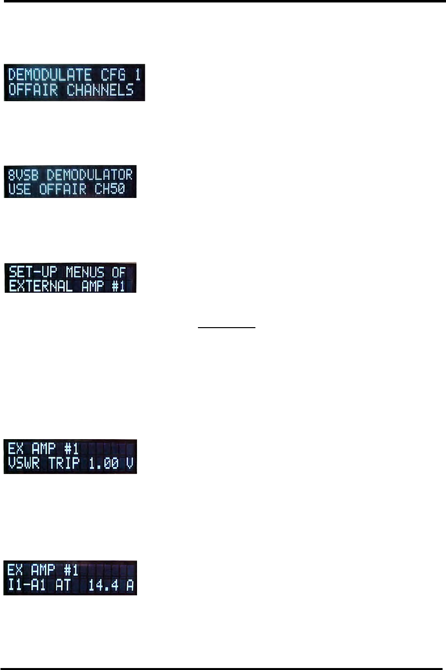
Innovator CHV0TD/RD-1 through CHV4TD/RD ATSC
Transmitter/Regenerative Translator w/DM8C Modulator Interface Description
Instruction Manual, Rev. 1 69
Figure 12.3.1: Device Setup - 8VSB Demodulator Channels Set Up Screen (RD)
Menu Level 8VSB Demodulator Setup Main Screen
Description This screen allows selection of the channel plan which can be
changed to either Off Air or Cable.
Figure 12.3.2: Device Setup - 8VSB Demodulator Channel Select Set Up Screen (RD)
Menu Level 8VSB Demodulator Setup Main Screen
Description This screen allows selection of the channel, for the channel plan
selected in the previous screen.
Figure 12.4: Device Setup – External Amplifier #1 (TD/RD)
Menu Level External Amplifier #1 Setup Main Screen
Description This screen provides access to the external amplifier #1 read /
write parameters. WARNING: THESE SCREEN VALUES ARE
USED TO IMPLEMENT PROTECTION CIRCUITS WITHIN THE
AMPLIFIER. FACTORY SET VALUES SHOULD NOT BE CHANGED
WITHOUT DIRECTION FROM AXCERA FIELD SERVICE.
NOTE: Shown below are the External Amplifier #1 Set-Up Screens. The External
Amplifier #2, #3 or #4 Set-Up Screens are presented in the same order if they are
present in the system.
Figure 12.4.1: Device Setup – External Amplifier #1 VSWR Trip Set Up Screen
(TD/RD)
Menu Level External Amplifier #1 VSWR Trip Setup Screen
Description This screen allows set up of the WSWR Trip level.
Parameter Range
Adjustment range is zero to 3.09 Volts. This value is unique for
each amplifier based on the output power and frequency.
Figure 12.4.2: Device Setup – External Amplifier #1 I1-A1 Current Set Up Screen
(TD/RD)
Menu Level External Amplifier #1 I1-A1 Current Setup Screen
Description This screen allows set up of the I1-A1 Current level.
Parameter Range Adjustment range is zero to 49.9 Amps.
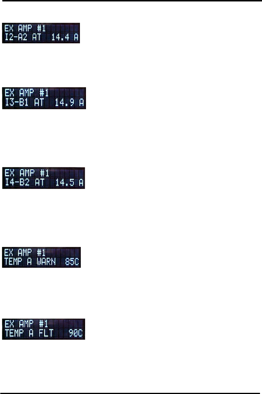
Innovator CHV0TD/RD-1 through CHV4TD/RD ATSC
Transmitter/Regenerative Translator w/DM8C Modulator Interface Description
Instruction Manual, Rev. 1 70
Figure 12.4.3: Device Setup – External Amplifier #1 I2-A2 Current Set Up Screen
(TD/RD)
Menu Level External Amplifier #1 I2-A2 Current Setup Screen
Description This screen allows set up of the I2-A2 Current level.
Parameter Range Adjustment range is zero to 49.9 Amps
Figure 12.4.4: Device Setup – External Amplifier #1 I3-B1 Current Set Up Screen
(TD/RD)
Menu Level External Amplifier #1 I3-B1 Current Setup Screen
Description This screen allows set up of the I3-B1 Current level. Some low
power external amplifiers may not monitor the I3-B1 current
signal.
Parameter Range Adjustment range is zero to 49.9 Amps.
Figure 12.4.5: Device Setup – External Amplifier #1 I4-B2 Current Set Up Screen
(TD/RD)
Menu Level External Amplifier #1 I4-B2 Current Setup Screen
Description This screen allows set up of the I4-B2 Current level. Some low
power external amplifiers may not monitor the I4-B2 current
signal.
Parameter Range Adjustment range is zero to 49.9 Amps.
Figure 12.4.6: Device Setup – External Ampl. #1 Temp. A Warning Set Up Screen
(TD/RD)
Menu Level External Amplifier #1 Temperature A Warning Setup Screen
Description This screen allows set up of the Device A temperature Warning
level.
Parameter Range Adjustment range is zero to 219C but a typical value is 85C.
Figure 12.4.7: Device Setup – External Ampl. #1 Temp. A Fault Set Up Screen
(TD/RD)
Menu Level External Amplifier #1 Device A Temperature Fault Setup Screen
Description This screen allows set up of the Device A Temperature Fault
level.
Parameter Range Adjustment range is zero to 219C but a typical value is 90C.
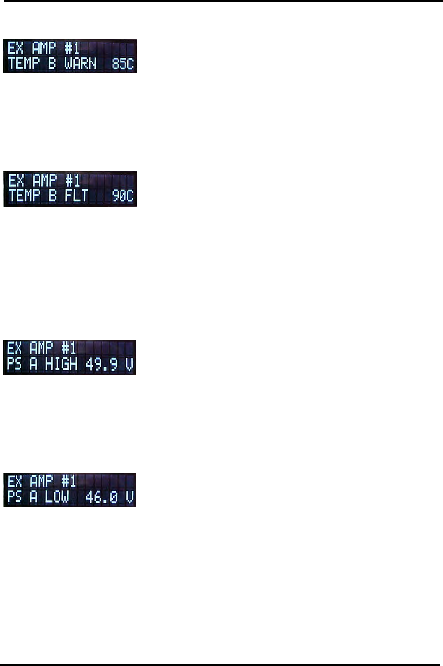
Innovator CHV0TD/RD-1 through CHV4TD/RD ATSC
Transmitter/Regenerative Translator w/DM8C Modulator Interface Description
Instruction Manual, Rev. 1 71
Figure 12.4.8: Device Setup – External Ampl. #1 Temp. B Warning Set Up Screen
(TD/RD)
Menu Level
External Amplifier #1 Device B Temperature Warning Setup
Screen
Description This screen allows set up of the Device B Temperature Warning
level.
Parameter Range Adjustment range is zero to 219C but a typical value is 85C.
Figure 12.4.9: Device Setup – External Ampl. #1 Temp. B Fault Set Up Screen
(TD/RD)
Menu Level External Amplifier #1 Device B Temperature Fault Setup Screen
Description This screen allows set up of the Device B Temperature Fault
level.
Parameter Range Adjustment range is zero to 219C but a typical value is 90C.
Figure 12.4.10: Device Setup – Ext. Ampl. #1 Power Supply A High Set Up Screen
(TD/RD)
Menu Level External Amplifier #1 Power Supply A High Setup Screen
Description This screen allows set up of the Power Supply A High level.
Parameter Range
Adjustment range is zero to 49.9 Volts. Value is set based on
nominal voltage of power supply which may be different for VHF
and UHF amplifiers.
Figure 12.4.11: Device Setup – Ext. Ampl. #1 Power Supply A Low Set Up Screen
(TD/RD)
Menu Level External Amplifier #1 Power Supply A Low Setup Screen
Description This screen allows set up of the Power Supply A Low level.
Parameter Range Adjustment range is zero to 49.9 Volts.

Innovator CHV0TD/RD-1 through CHV4TD/RD ATSC
Transmitter/Regenerative Translator w/DM8C Modulator Interface Description
Instruction Manual, Rev. 1 72
Figure 12.4.12: Device Setup – Ext. Ampl. #1 Power Supply B High Set Up Screen
(TD/RD)
Menu Level External Amplifier #1 Power Supply B High Setup Screen
Description This screen allows set up of the Power Supply B High level.
Some low power external amplifiers may not contain a B-side
power supply.
Parameter Range Adjustment range is zero to 49.9 Volts.
Figure 12.4.13: Device Setup – Ext. Ampl. #1 Power Supply B Low Set Up Screen
(TD/RD)
Menu Level External Amplifier #1 Power Supply B Low Setup Screen
Description This screen allows set up of the Power Supply B Low level. Some
low power external amplifiers may not contain a B-side power
supply.
Parameter Range Adjustment range is zero to 49.9 Volts.
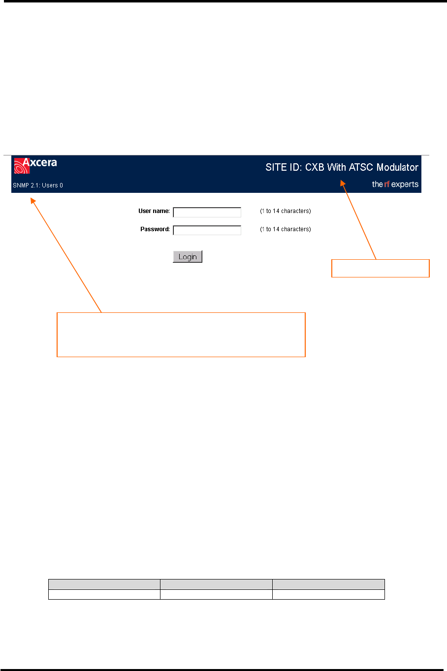
Innovator CHV0TD/RD-1 through CHV4TD/RD ATSC
Transmitter/Regenerative Translator w/DM8C Modulator Interface Description
Instruction Manual, Rev. 1 73
(Optional) Innovator CX Series Web Ethernet Interface Kit (1313100)
The Innovator CX transmitter is available with an optional Ethernet interface
package. Axcera part number (1316423) is the Axcera part number for an Ethernet
Interface kit that provides an SNMP interface to transmitter parameters, serves
HTML web pages, and provides a link to the modulator web pages. This option may
be added to the Innovator CX transmitter if it was not originally installed at the
factory. NOTE: Mozilla Firefox is the preferred browser for this WEB Ethernet
interface kit.
Figure 13: Typical Ethernet User Log In Screen
Once a connection has been established, the web interface can be launched by
entering the IP address of the Innovator CX Ethernet Controller as a URL in the
browser of the remote computer. A login screen will be displayed prompting for a
user name and password, which are case sensitive.
The controller has three levels of user access: Administrative, Read/Write and Read
Only. Administrators have full access to transmitter controls and controller
configuration. Read/Write users have full access to transmitter controls and can
change all controller configurations except for the user name and password accounts.
Read Only users can view all transmitter parameters and the event log entries but
they can not change the transmitter's state, clear faults, clear the event log or
configure the Ethernet parameters.
Five unique login accounts are available. The factory default user name and
password for account number one are:
User Name Password Access Level
admin axcera Administrator
The user name and password of account number one may be reset to factory default
values through a setup screen of the transmitter.
Indicates SNMP with package software version and
number of users currently on-line.
NOTE: Only 5 simultaneous on-lines users are allowed.
Unique Site ID value
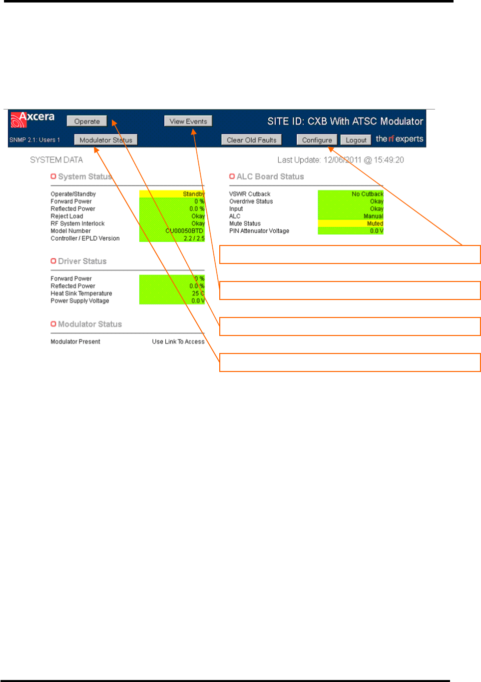
Innovator CHV0TD/RD-1 through CHV4TD/RD ATSC
Transmitter/Regenerative Translator w/DM8C Modulator Interface Description
Instruction Manual, Rev. 1 74
After logging in, the main control/monitoring screen is displayed. Administrators
have the ability to change the transmitter's operate / standby state, and configure
the application. All users have the ability to view the transmitter's event log, and
review system parameters. Refer to Figure 14 for a sample of the main
control/monitoring screen.
Figure 14: Typical Ethernet Main Control/Monitoring Screen
Color Key:
Green = Okay or Normal Operation
Yellow = Warning, But Not faulted
Red = Currently Active Fault
Orange = Old or Previously Latched Fault
If an item on screen is Orange, a latched fault is present. Activating the 'Fault
Reset' button will reset any latched faults, clears the transmitter's event log and
causes the parameter to display normally.
The date and time of the last message received by the web page browser is present
to assure connectivity. If the browser does not receive a new set of data from the
Ethernet Controller, it will show the last update field with a yellow background
indicating a connection problem is present.
From the main page, administrators and accounts with read/write access may
change the web interface settings by activating the ‘Configure’ button near the top of
the screen.
This command button opens the modulator's web pages.
This command button places the transmitter in Operate.
This command button switches to the Events Log page.
Activate this command button to configure the transmitter.
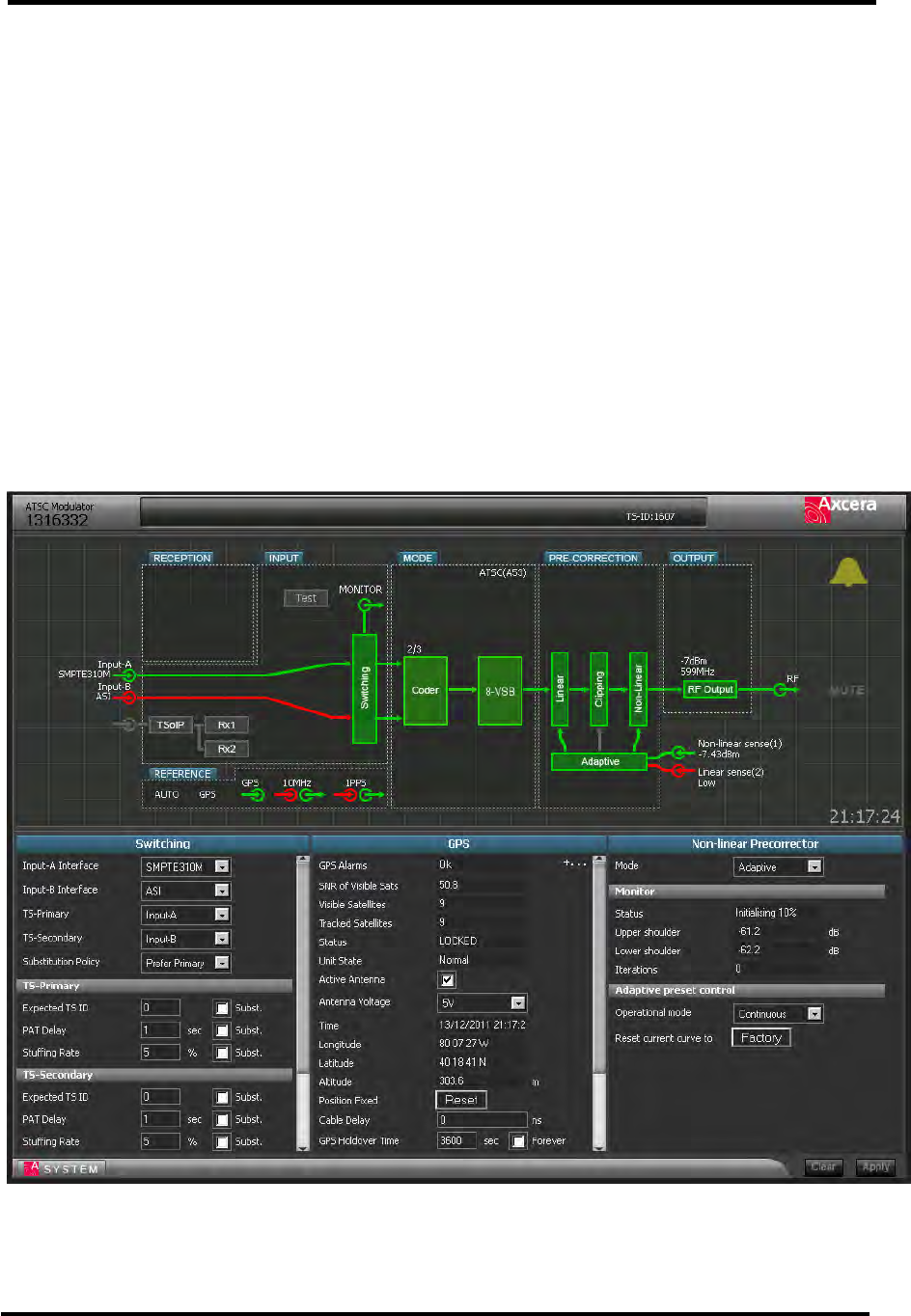
Innovator CHV0TD/RD-1 through CHV4TD/RD ATSC
Transmitter/Regenerative Translator w/DM8C Modulator Interface Description
Instruction Manual, Rev. 1 75
Modulator Web Interface
Access to view the Modulator WEB Interface is available by selecting the 'Modulator
Status' button.
The modulator requires a valid username and password for login access. When
launched from the Axcera CX web interface, the login address of username /
password information is automatically included in the login script. Since username
and passwords of the modulator are fixed, we recommend modulator web pages are
only launched from the main CX web page using the modulator command button. .
NOTE: Mozilla Firefox is the preferred browser for this modulator WEB interface.
Three levels of access are provided. 1) Administrators have full read / write control
of the modulator and they can configure all system parameters of the modulator. 2)
An Operator has read / write control of most modulator parameters and limited
ability to configure system parameters. 3) An Observer has read only access to the
modulator parameters.
Figure 15: Sample Modulator Page
The modulator's web page contains an upper form and three lower forms. The upper
form always shows a graphical representation of the modulators system. A Block of
the upper form can be dragged into any one of the three lower forms to view specific
Innovator CHV0TD/RD-1 through CHV4TD/RD ATSC
Transmitter/Regenerative Translator w/DM8C Modulator Interface Description
Instruction Manual, Rev. 1 76
details of the specific system. In the above figure, the "Switching" block of the Input
System was dragged into the lower left form. The GPS block of Reference was
dragged into the lower middle form and the Nonlinear block of Precorrection was
placed into the lower right form.
Figure 16: Additional Forms
Activating the "System" icon located at the lower left corner of the page accesses
additional forms. The sample screen above is typical of forms available to an
administrator. Operators and Observers will have different forms available.
Innovator CHV0TD/RD-1 through CHV4TD/RD ATSC
Transmitter/Regenerative Translator w/DM8C Modulator Interface Description
Instruction Manual, Rev. 1 77
Access to view the transmitter's event log is available by selecting the 'View Events'
button.
Figure 17: Typical Event Log Screen
This screen allows an operator to view events and to determine the time between
events. Events are logged in the order they are received. If more than 200 events
are detected, the transmitter's System Controller drops the oldest event to record
the new event. Transferring of events from the transmitter's System Controller and
the Ethernet Controller is scheduled so that device details are continuously
monitored. Therefore the event log screen may update a few seconds behind the
transmitter display when the log is full or changing quickly.
Each event record indicates the event number, the number of events, an occurrence
counter and text describing the event. The occurrence counter keeps track of the
number of times a specific event has occurred since the log was last cleared. Up to
99 occurrences are available for each event.
To view the next set of twenty events, activate the 'Next' button. If viewing events
higher in the log, the 'Previous' button allows you to return to prior events.
Innovator CHV0TD/RD-1 through CHV4TD/RD ATSC
Transmitter/Regenerative Translator w/DM8C Modulator Interface Description
Instruction Manual, Rev. 1 78
Figure 18: Ethernet Configuration Screen
When entering a site ID, be sure to not use special characters except underscores,
dashes, and forward slashes. Changes to the transmitter's output power are
available to administrators when the transmitter is operating. Once changed, the
menu defaults back to the main display page and the systems forward power is
noted as changing.
The screen above displays SNMP parameters and allows an operator to send a test
trap. If this system did not have SNMP enabled, then fields would not be populated
and the 'Send Test Trap' button would not be present. New event log entries
including an activated test trap are automatically forwarded to SNMP agents specified
to receive trap messages. Trap messages do not need to be acknowledged by an
agent.
NOTE: The Innovator CX controller does not use DHCP addresses – TCP/IP settings
must be fixed and entered manually. A crossover cable may be needed if connecting
directly from a computer to the Innovator CX Transmitter.
To manage user accounts, administrators may click the ‘Manage Accounts’ button
near the top of the configure screen.

Innovator CHV0TD/RD-1 through CHV4TD/RD ATSC
Transmitter/Regenerative Translator w/DM8C Modulator Interface Description
Instruction Manual, Rev. 1 79
Figure 19: Typical Manage Accounts Screen
The Innovator CX Ethernet controller supports up to 5 different user accounts. To add
or change one of the accounts, click the Add/Change button in the row of the account
you want to modify, then enter the desired name, password, and administrator or
read/write access rights for the user and click save.
NOTE: The transmitter's set up menus contain a Reset Ethernet User ID screen.
This screen allows a user to reset the first account User Name and
Password. The Yes or No selection can be changed by pushing the Up or
Down Button. After the selection has been made, the user needs to
depress the right or left arrow and then the display will ask “PUSH ENTER
TO ACCEPT CHANGES”. If the ENTER button is depressed, the change will
be accepted. If any other button is depressed, the change will not be
made. If Yes is selected on the screen, and accepted, the User name and
Password will reset to the factory default of admin / axcera.
Activate the 'Back' button to return to the main control/monitoring screen.
When you have completed using the web interface, please remember to log out via
the 'logout' button at the top of the control/monitoring screen.

Innovator CHV0TD/RD-1 through CHV4TD/RD ATSC SNMP Ethernet
Transmitter/Regenerative Translator Interface Description
Instruction Manual, Rev. 1 80
SNMP Interfaces
The Innovator CX Ethernet Controller implements Simple Network Management Protocol
(SNMP). SNMP is a standardized method of transferring information from one electronic
device to another. SNMP is typically used to remotely control and monitor several
transmitter devices from a centralized network management system (NMS). SNMP is a
communication method between two applications and is not a graphical user interface.
Therefore, SNMP functionality is included along with web page server functionality.
SNMP is used to gather information or set control states but it requires additional
computer applications for operator monitoring and control.
The Innovator CX Ethernet controller implements SNMP version 2 (SNMP v2) using a
Management Information Base (MIB). The MIB file defines all SNMP parameters of the
transmitter, specifies the format of data, and orders the presentation of the parameters
using a hierarchical namespace containing object identifiers (OID). Each OID identifies a
variable that can be read, read and set, or only set via SNMP commands.
SNMP functionality also provides for alert messages that are issued from the Ethernet
Controller to one or two network computers. A SNMP trap message is sent only once
and is not acknowledged by the receiving device. The Ethernet Controller issues a trap
message when data is added to the transmitter Event log (either activation of a fault or
when a fault is cleared), or when the transmitter operate/standby status changes.
SNMP Configuration
The Ethernet Controller's TCP/IP Address, Subnet Mask, and Gateway must be
configured with static values that are valid within your network. Dynamic Host
Configuration Protocol (DHCP) is not implemented; however access to these
configuration parameters is available through the front panel setup menus of the
Innovator CX.
The Innovator CX's SNMP MIB allows up to two SNMP trap destinations. The trap
destination values can be set through WEB pages. The TCP/IP address of a trap
processing computer can also be configured through the SNMP parameters called
'site_trap_adr1' and 'site_trap_adr2'. To clear a previously configured trap destination
and cause the system not to issue traps to a specific address, set the value to
'000.000.000.000'.
Reading of SNMP values is done with the message's community access set to 'public'.
When setting SNMP values, a default community access level of 'private' is used. Future
implementations of the Ethernet SNMP agent may allow for the set community access
level to be defined through the device's web server.

Innovator CHV0TD/RD-1 through CHV4TD/RD ATSC Board Descriptions
Transmitter/Regenerative Translator
Instruction Manual, Rev. 1 81
Circuit Descriptions of Boards in the CHV0xD-1 & CHV0xD-4 System
(A1) 8 VSB Demodulator Board (1308275) - Only used with RD operation
Overview
The 8 VSB demodulator assembly receives an off air 8 VSB signal on any VHF or
UHF channel and demodulates this to an MPEG-2 transport stream that is per the
SMPTE-310M standard. The input to the assembly is at an “F” style connector on
the shielded tuner and can be at a level of –8 to –78 dBm. The tuner (TU1)
down converts the RF channel to a 44 MHz IF signal. This signal is the input to
the digital receiver chip U1. The digital receiver chip subsequently decodes the IF
and delivers an MPEG-2 transport stream on a parallel data bus to a
programmable logic array, U8. U8 clocks the asynchronous MPEG data from the
receiver chip and outputs a synchronous data stream at a 19.39 MHz rate to
buffer/driver U11. U11 subsequently drives the output at J13 to a lower level
that is AC coupled out of the board.
Microcontroller Functions
A microcontroller, U17, is provided on this assembly to supervise the operation of
the receiver chip and the tuner. In addition, the microcontroller also interfaces to
the front panel LCD display via connector J24 and pushbutton interface on J27.
On power up, the microcontroller sets the tuner to the last channel that was
selected when the unit was powered down. In addition, the microcontroller also
configures the digital receiver to operate as an 8 VSB receiver. The
communication between all of the devices on this board is via an I2C serial bus
that is local to this board.
Jumper and DIP Switch Settings
This board can be used in various assemblies. When this assembly is installed in
the Innovator CX product, the jumpers on J7 and J8 should be placed between
pins 2 and 3 for normal operation. The DIP switch SW1 should be configured as
indicated in Table 12.
Table 12: Innovator CX Receive /Demodulator/Transcoder Dip Switch SW1
Position
Function When Switch is Off When Switch is On
SW1-1 Tuner Type Original Tuner (DTT765xx) Recent Tuner (DTT7680x)
SW1-2 Signal Strength
Gain Gain = 8.0 Gain = 9.3
SW1-3 Special Channel
Plan Normal Channels 2, 3, or 4 are offset
up 4 MHz
SW1-4 Reserved for Future
SW1-5 Reserved for Future
SW1-6 Reserved for Future
SW1-7 Reserved for Future
SW1-8 Operation Type Transcoder Operation Innovator CX Operation
NOTES: SW1-8 operation is available in software versions greater than or equal to 2.3
with hardware versions greater than or equal to D0, unless the board was factory
modified.
These switch positions are factory set for your system and should not be changed.

Innovator CHV0TD/RD-1 through CHV4TD/RD ATSC Board Descriptions
Transmitter/Regenerative Translator
Instruction Manual, Rev. 1 82
(A2) Digital Modulator Board DM8C (1316332)
The digital modulator board accepts either ASI or SMPTE-310 input at SMA
connectors J13 or J4. Regenerative transmitters will have a connection on J14
from the 8 VSB demodulator board in a RD system.
(A5) ALC Board, Innovator CX Series (1315006)
The ALC Board in the Innovator CX series transmitter is used to control the RF drive
power to the RF amplifier chain in the system. The board accepts an RF input signal at a
nominal input level of -3 dBm average power and amplifies it to whatever drive level is
necessary to drive the final RF amplifier in the drawer to full power. The input signal to
the board at J1 is split by U4, with one half of the signal driving a PIN diode attenuator,
DS1 and DS2, and the other half driving a detector, U13, that is used to mute the PIN
attenuator when there is no input signal. The output of the PIN attenuator is sent to two
cascaded amplifiers, U2 and U3, which are capable of generating +10 dBm average
power from the board at J2.
The PIN attenuator is driven by an ALC circuit or by a manual fixed voltage bias,
depending on the position of switch S1. When the switch is pointing to the left, looking
from the front of the drawer, the ALC circuit is enabled. When the switch is pointing to
the right, the ALC circuit is disabled and the PIN attenuator is controlled through the
Manual gain pot R62. When the switch is in either ALC or manual, the voltage in the
unused circuit is preset low by the circuitry connected to pins 4-6 on SW1. This allows
the RF power to ramp up slowly to full power when the switch changes positions. CR8,
C33 and associated components control the ramp up speed of the manual gain circuit.
CR9, C42 and their associated circuits do the same thing for the ALC circuit. The
practical effect of this is to preset the RF drive power to near zero output power when
enabling and disabling the ALC, followed by a slow controlled ramp up of power.
The ALC circuit normally attempts to hold the drawer output power constant, but there
are four faults that can override this. These faults are Input Fault, VSWR Cutback Fault,
VSWR Shutdown Fault and Overdrive Fault.
The Input Fault is generated by comparator U7C and presets the PIN attenuator and ALC
circuit to maximum attenuation whenever the input signal drops below about -7 dBm.
Test point TP2 allows the user to measure the detected input voltage.
The VSWR cutback circuit is set so that the ALC circuit will start reducing RF drive once
the Reflected power reaches a level of about 6% and will keep reducing the drive to
maintain that level. The cutback is generated by U8A, U8B and their associated
components that diode-or the metering voltages. The forward power is scaled to
2V = 100 % and the reflected power is scaled to 2V = 25%. The Reflected metering
voltage is doubled again by U8B so that when the voltage of U8B exceeds the voltage at
the output of U8A, the reflected power takes over the ALC circuit. Once the U8B voltage
drops below the forward power at U8A, the forward power takes over again.
The VSWR shutdown circuit will shut the drawer down if the Reflected power increases to
15% or higher, which can happen if the drawer sees reflected power when the ALC is in
manual.

Innovator CHV0TD/RD-1 through CHV4TD/RD ATSC Board Descriptions
Transmitter/Regenerative Translator
Instruction Manual, Rev. 1 83
The Overdrive protection looks at a sample of the RF signal that is applied to J1 of the
board. The peak level of this signal is detected and can be measured on TP1. This
voltage is applied to a comparator with the threshold set by R38. If this threshold is
exceeded, the ALC circuit mutes then ramps up to try again. This circuit also works in
manual gain as well.
(A6) Amplifier Assembly (1313959) – Used in the CHV0xD-1 Drawer
The (A6) Amplifier Assembly (1313959) is made up of (A6-A1) the VHF HB Pre-Driver
Assembly (1313899) and (A6-A2) the 100 Watt Amplifier Pallet, Italmec (1313484).
The ALC Board (1315006) is also part of this assembly. The assembly has
approximately 36 dB of gain.
(A6-A1) VHF HB Pre-Driver Assembly (1313899)
The VHF HB Pre-Driver Assembly (1313899) consists of a driver and a parallel
connected final amplifier stage, which has a total gain of approximately 23 dB.
The input RF at J1 connects through a matching network consisting of R11-R13 to
a splitter IC Z1. The split outputs connect to parallel-connected push-pull 1 Watt
high linearity amplifier ICs (U1& U4) operating in class AB each with
approximately 17 dB of gain. The board uses a power supply voltage of +48VDC
that connect to J6. The +48VDC is filtered on the board and connected to the
step down transformer T1 which produces a +12VDC output that is used by the
two amplifier ICs (U1 & U4). The two amplified outputs are connected to a
combiner IC Z2. The combined output connects through a directional coupler U6
to J2, the RF output jack of the board. The directional coupler provides an RF
sample at J4 that is used by an external overdrive protection circuit located on
the (A6-A3) ALC Board. The output of the pre-driver amplifier assembly at J2
connects to the RF Input connection on the (A6-A2) 100W Amplifier Pallet,
Italmec.
(A6-A2) 50 Watt Amplifier Pallet, Italmec (1313484)
The 50 Watt Amplifier Pallet, Italmec is made by Italmec for Axcera’s use. This
broadband amplifier operates in the frequency range of 170 to 240 MHz. The
amplifier is capable of delivering a maximum output power of 25 Watts digital,
with an amplification factor of approximately 24 dB. The RF output of the pallet
is wired to J2 the RF output jack of the 20W driver amplifier assembly. The
output of the 20W driver amplifier assembly is cabled to the J1 on (A7) the
output metering detector board (1313747).
(A6) 200 Watt Driver Amplifier Assembly (1315010 used w/Axciter Drawer or
1313912 used in all other applications) – Used in the CHVxD-4
The (A6) Amplifier Assembly (1315010 used w/Axciter Drawer or 1313912 used in all
other applications) is made up of (A6-A1) the 50 Watt Amplifier Pallet, Italmec
(1313484) and (A6-A2) the 500 Watt Amplifier Pallet, Italmec (1313581). The ALC
Board (1315006) is also part of this assembly. The assembly has approximately 36 dB
of gain.
(A6-A1) 50 Watt Amplifier Pallet, Italmec (1313484)

Innovator CHV0TD/RD-1 through CHV4TD/RD ATSC Board Descriptions
Transmitter/Regenerative Translator
Instruction Manual, Rev. 1 84
The 50 Watt Amplifier Pallet, Italmec is made by Italmec for Axcera’s use. This
broadband amplifier operates in the frequency range of 170 to 240 MHz. The
amplifier is capable of delivering a maximum output power of 25 Watts digital,
with an amplification factor of approximately 24 dB. The RF output of the pallet
is wired to J2 the RF output jack of the 20W driver amplifier assembly. The
output of the 20W driver amplifier assembly is cabled to the RF input connection
on (A6-A2) the 500 Watt Amplifier Pallet, Italmec.
(A6-A2) 500 Watt Amplifier Pallet, Italmec (1313581)
The 500 Watt Amplifier Pallet, Italmec is made by Italmec for Axcera’s use. This
broadband amplifier operates in the frequency range of 170 to 240 MHz. The
amplifier is capable of delivering a maximum output power of 200 Watts digital,
with an amplification factor of approximately 25 dB. The RF output of the pallet
is wired to J2 the RF output jack of the 200W driver amplifier assembly. The
output of the 200W driver amplifier assembly is cabled to the J1 on (A7) the
output metering detector board (1313747).
(A7) Output Metering Detector Board (1313747)
The (A7) Output Detector Board provides forward (2V=100%) and reflected (2V=25%)
power samples to the CX Control Board for metering and monitoring purposes. R7 is the
reflected power calibration pot and R23 is the forward power calibration pot. A Forward
power sample connects to J4 (-10 dBm typical) on the board which is cabled to the front
panel sample jack of the drawer. The RF output of the board will vary depending in
which system it is located, is at J2, which is cabled to J9 the RF Output Jack of the
amplifier drawer.
(A8) Control Card, Innovator CX (1312543)
The Innovator CX control board provides the overall system control for the CX system.
There are two main elements of the board U7 and U9. U7 is a programmable logic
device that is loaded with firmware which provides the overall system control. It decides
whether or not to allow the system to generate RF output power, and turns the power
supply on and off depending on whether or not it is receiving any faults generated on
board or faults generated externally. The second major component of the board is the
microcontroller U9, which controls the front panel indications and drives the display.
The U9 microcontroller is not involved in the decision making process, U7 does that.
Rather, it is layered on top of U7 and is the EPLD's interface to the outside world.
Information is passed between the microcontroller and the EPLD. The microcontroller
communicates information to and from the front panel and sends the EPLD the
information it needs to decide whether or not to allow the system to turn on. The front
panel viewable LEDs DS3 for Operate/Standby and DS4 for Status indicate the current
operating condition of the system are mounted on and controlled by this board. The U9
microcontroller can also communicate, using the Optional Ethernet Kit, with a daughter
card that allows the user to view remote control parameters via a web Ethernet
interface.
The ±12 VDC and +5 VDC from the (A9) power supply are routed to the other boards in
the drawer through this board. The (A10) +48 VDC power supply connects the +48 VDC
to the board at J19-1 with 4 common. The ±12 VDC and +5 VDC input voltages to this
board is connected through J21 and filtered before being connected to the rest of the
board. +12 VDC connects through J21-1, +5VDC through J21-2 & 3, and -12 VDC
through J21-6. Common connections for the input voltages are connected to J21-4 & 5.
The ±12 VDC and +5 VDC are used on this board and also routed to the other boards in
the drawer through this board. The +3.3 VDC for the microcontroller and programmable

Innovator CHV0TD/RD-1 through CHV4TD/RD ATSC Board Descriptions
Transmitter/Regenerative Translator
Instruction Manual, Rev. 1 85
logic array, mounted on the board, is provided by the voltage regulator IC U6 from the
filtered +5 VDC input. The output of U6 can be adjusted to +3.3 VDC using R120.
(A9 & A10) Power Supplies used in CHV0xD-1 and CHV0xD-4
Voltages for the operation of the boards in the drawer are generated by (A9) a +5VDC
and ±12VDC power supply and (A10) a +48VDC power supply. The 230VAC input to the
drawer connects through the AC power cord at J10, the power entry module located on
the rear panel of the drawer.
An On/Off 10A/250VAC circuit breaker is part of the power entry module. With the
circuit breaker switched On, the (L) line input is wired to F1 a 10 Amp fuse for over
current protection. The AC lines are connected to terminal block TB1, which distributes
the AC to (A9 and A10) the two DC power supplies. There are two varistors, mounted
on TB1, connected from the line input to neutral and to ground for surge protection.
The AC also connects to the (A11) fan mounted on the rear panel of the driver drawers
In CHV0xD-1 systems the fan is connected to the A10 power supply and will operate
when the (A10) Power supply is enabled. In the CHV0xD-4 the small fan will run when
AC is applied to the drawer and the circuit breaker is switched On. The large (A32) fan
is connected to the A10 power supply and will operate when the (A10) Power supply is
enabled. The +5VDC and ±12VDC outputs of the (A9) power supply connects to the
terminal block (TB2) that distributes the DC to the boards in the drawer. Some of the
+5VDC and ±12VDC outputs connect directly to the 8 VSB Demodulator and 8 VSB
Modulator boards while the other outputs connect through the CX Control Board to the
IF Precorrector, the Digital Upconverter, the ALC, the Amplifier Assembly and the Output
Metering Detector Boards.
The +48VDC outputs of the (A10) power supply connect to the (A8) CX Control Board,
which then supplies the switched +48VDC to the (A6) Amplifier Assembly. In CHV0xD-1
drawers the DC output of the (A10) power supply also connects to the (A11) fan
mounted on the rear panel, which will operate when AC is applied to the drawer, the
On/Off circuit breaker is On and the (A10) power supply is operating.
Circuit Description of External System Metering Board which is only used in
Transmitters with multiple external Amplifier Drawers
(A5) System Metering Board (1312666)
The function of the System Metering Board is to detect forward and reflected output power
samples and generate output voltages that are proportional to the power levels of the
sampled signals for use by the control monitoring assembly in the exciter/driver drawer.
There are two identical signal paths on the board: one for forward power and one for
reflected power. A sample of the forward output power, from the external (A11) output
coupler, enters the board at the SMA jack J3. The signal is filtered and connected to
resistors R5, R3 and R6 that form an input impedance-matching network to Pin 3 on U1.
The forward power signal is detected by the RF detector IC U1. The detected output at
pin 7 is split with one half connected to the forward average calibration pot R7, digital,
which adjusts the level of the signal connected to Pin 11 on U2. The other half of the split
is connected to the peak calibration pot R18, analog, which adjusts the level of the signal
connected to Pin 8 on U2. U2 is a Bilateral Switch IC whose output, digital or analog, is
controlled by the selection of the modulation type in the exciter/driver drawer. In this
Innovator CHV0TD/RD-1 through CHV4TD/RD ATSC Board Descriptions
Transmitter/Regenerative Translator
Instruction Manual, Rev. 1 86
BTC transmitter the average, digital, output connects to the amplifier IC U3A that is wired
to the SYS_FWD and RMT_FWD Power Metering Outputs. A reading of 2 VDC measured at
TP1 is equal to a 100% Forward Power reading on the meter. The SYS_FWD level
connects to J9 on the board that is cabled to J11 on the exciter/driver drawer for use in
the control monitoring assembly. The RMT_FWD level connects to J10 on the board for
use by remote control and monitoring.
A sample of the reflected output power, from the external (A11) output coupler, enters
the board at the SMA jack J8. The signal is filtered and connected to resistors R26, R22
and R27 that form an input impedance-matching network to Pin 3 on U6. The reflected
power signal is detected by the RF detector IC U6. The detected output at pin 7 is
connected to the reflected calibration pot R25, which adjusts the level of the signal
connected to the amplifier IC U3B that is wired to the SYS_RFLD and RMT_RFLD Power
Metering Outputs. A reading of 2 VDC measured at TP2 is equal to a 25% Reflected
Power reading on the meter. The SYS_RFLD level connects to J9 on the board that is
cabled to J11 on the exciter/driver drawer for use in the control monitoring assembly. The
RMT_RFLD level connects to J10 on the board for use by remote control and monitoring.
+12 VDC enters the board at J9-1, from the exciter/driver drawer and is connected
through a filter and isolation circuit consisting of C31, C14 and L5 before it is connected to
the regulator IC U5. U5 supplies the +5 VDC needed for operation of the ICs on the
board. The +5 VDC is connected through a filter circuit consisting of C15, C19 and C21
before it is connected to the rest of the board.
Circuit Descriptions of Boards in the external VHF amplifier Drawer
(A7) Amplifier Control Board (1312260)
Amplifier Control Board
The Amplifier Control Board is mounted in the top front facing the rear of the Amplifier
Drawer as shown above.
The Amplifier Control Board uses a Programmable logic device, U12, to control the
amplifier drawer. It takes an enable signal from an external driver drawer, and turns
the power supplies on whenever the driver has told it to turn on, unless it detects faults
internal to the drawer. The board monitors the forward and reflected power, the
heatsink temperature, the pallet currents, and the power supply voltage and will
generate alarm signals if any of those parameters exceed safe limits. The amplifier
drawer has no front panel display other than a two LEDs, one for Status and one for
Enable. The board sends all its output information, including the forward and reflected
levels, back to the driver drawer, through J4, so the information can be displayed on
that drawer's LCD Display. The board will generate a Red Blinking Status LED if it
detects an alarm, fault, prompting the operator to look at the LCD display on the driver
drawer to see what fault has occurred.
A CHVB transmitter System can have up to 4 external amplifier drawers and since they
are all the same, without differences in the wiring harness, there needs to be a way to
identify which amplifier drawer is which. The rotary switch SW1 is used to specify the
SW1

Innovator CHV0TD/RD-1 through CHV4TD/RD ATSC Board Descriptions
Transmitter/Regenerative Translator
Instruction Manual, Rev. 1 87
amplifier ID number which generates a unique serial address so that the individual
amplifier drawers will respond when polled for information.
The +5 VDC inputs to this board are routed through J4-8 and J5-8. The +5 VDC inputs
are diode Or connected so that either the +5VDC from the (A8) power supply or the
+5VDC from the (A9) power supply will operate the board. The +5VDC is split with one
output connected to U1 a voltage regulator IC, which provides +5V and +5V_ANALOG as
outputs. The +5 VDC is filtered before being connected to the rest of the board. The
other +5 VDC output is connected to the regulator IC U2 that supplies +3.3 V to the
microcontroller and programmable logic array.
(A10) Current Metering Board (1309130)
The current metering board measures the current into the RF output amplifier pallets
and supplies this value to the control board. In the VHF amplifier drawer, there are two
sensing circuits which are used. In the VHF amplifier drawer there are four sensing
circuits which are used. Each circuit has two parallel .01Ω series current sensing
resistors and a differential input IC that supplies a voltage output that is proportional to
the current for metering purposes. The +48VDC from the (A8) power supply connects
to TB2 and TB4 on the board. The +48VDC from the (A9) power supply connects to TB8
and TB10 on the board. The +48VDC input at the TB2 input senses the current to the
(A1) output amplifier pallet through TB1 on the board. The +48VDC input at the TB4
input senses the current to the (A2) output amplifier pallet through TB3 on the board.
The +48VDC input at the TB8 input senses the current to the (A3) output amplifier pallet
through TB7 on the board. The +48VDC input at the TB10 input senses the current to
the (A4) output amplifier pallet through TB9 on the board.
The two or four sensing circuits are identical therefore only one will be described. For
the (A1) amplifier pallet, the +48VDC from the (A8) switching power supply connects to
TB2. R1 and R2 are the parallel .01Ω current sensing resistors which supplies the
voltage values to the U1 current sense amplifier IC. R11 is a gain adjust, which is
adjusted to eliminate any rSense Error and to place the OpAmp output at 2.61V for
40Amps sense as measured at TP3. The current sense output at J1-1 connects to the
(A7) control board for metering purposes.
(A5) 2 Way VHF Splitter Board (1313941)
The 2 way splitter board takes the RF Input at J1 (≈12.5 Watts ATSC) on the board and
splits it into two equal outputs (≈5Watts ATSC) that connect to the inputs of the two
amplifier pallets at J1.
(A2 & A3) 500 Watt LDMOS Amplifier Pallets (1313581)
There are two 500 Watt Amplifier Pallets mounted on the Amplifier Heatsink Assembly.
Each of the amplifier pallets has approximately +25dB of gain for the VHF HB frequency
range of 170 to 230 MHz. The pallets operate Class AB and generate 200 Watts ATSC
with an input of 1 Watt ATSC.
(A6) 2 Way VHF Combiner Board (1313969)
The 2 way combiner board takes the two RF Inputs at J4 & J5 (≈200Watts ATSC) on the
board and combines them to a single output (≈400Watts) at J1 that connects to J2 the
7/16” (1.1cm) Din RF output jack of the drawer.

Innovator CHV0TD/RD-1 through CHV4TD/RD ATSC Board Descriptions
Transmitter/Regenerative Translator
Instruction Manual, Rev. 1 88
(A8 & A9) VHF Amplifier Drawer Power Supplies
The 230VAC, needed to operate the drawer, connects through the AC power cord at J3,
the power entry module located on the rear panel of the drawer. The AC lines are
connected to a terminal block TB1 to which the circuit breaker(s) connect. There are
two On/Off 20A/250VAC circuit breakers that are mounted on the back panel of the
drawer on either side of J3 the AC input jack. NOTE: In CHV400 Amplifier drawer there
is one circuit breaker. With the circuit breaker(s) switched On, the AC is distributed to
the one (A8) or two (A8 and A9) DC power supplies. In a standard CHV400B amplifier
drawer one 20 Amp circuit breaker CB1 connects the AC to the (A8) DC power supply.
In all power amplifier drawers, TB1 has three varistors (VR1-VR3) connected across the
AC input lines for surge and over voltage protection. The AC input connected to TB1 is
wired to 2 amp fuses that is connected to the two fans (A11 & A12) mounted on the rear
panel of the drawer. Both fans will run immediately when AC is applied to the drawer.
The +5VDC for the operation of the amplifier control board in the drawer is generated by
the (A8) or both the (A8 & A9) power supplies at J1-9 on each power supply. The
+5VDC from the (A8) power supply connects to J4-8 and the +5VDC from the (A9)
power supply connects to J5-8 on the control board. The +5VDC is produced when AC is
connected to the drawer and the CB1 and/or the CB2 circuit breakers are turned On.
Either or both power supplies provides the +5VDC for use by the control board.
The +48VDC needed by the amplifier modules on the heatsink assembly is generated by
the (A8 & A9) power supplies in a 750 and 1000W amplifier drawers. In a standard
CHV400 amp drawer there is only the (A8) power supply. The power supplies will
operate when AC is connected to the drawer, the CB1 circuit breaker for the (A8) power
supply and the CB2 circuit breaker for the (A9) power supply, are turned On and a Low
is provided on the Inhibit Line that connects to J1-6 on the power supplies from the
control board. The CB1 circuit breaker supplies the AC to the (A8) power supply which
provides the +45VDC to the (A2) and (A3) amplifier pallets. The CB2 circuit breaker
supplies the AC to the (A9) power supply which provides the +48VDC to the (A4) and
(A5) amplifier pallets.
Circuit Descriptions of Boards in the CHV500B/600B, 500/600 Watt ATSC
Amplifier Drawer
(A7) Amplifier Control Board (1312260)
Amplifier Control Board
The Amplifier Control Board is mounted in the top front facing the rear of the Amplifier
Drawer as shown above.
The Amplifier Control Board uses a Programmable logic device, U12, to control the
amplifier drawer. It takes an enable signal from an external driver drawer, and turns
the power supplies on whenever the driver has told it to turn on, unless it detects faults
internal to the drawer. The board monitors the forward and reflected power, the
heatsink temperature, the pallet currents, and the power supply voltage and will
SW1

Innovator CHV0TD/RD-1 through CHV4TD/RD ATSC Board Descriptions
Transmitter/Regenerative Translator
Instruction Manual, Rev. 1 89
generate alarm signals if any of those parameters exceed safe limits. The amplifier
drawer has no front panel display other than a two LEDs, one for Status and one for
Enable. The board sends all its output information, including the forward and reflected
levels, back to the driver drawer, through J4, so the information can be displayed on
that drawer's LCD Display. The board will generate a Red Blinking Status LED if it
detects an alarm, fault, prompting the operator to look at the LCD display on the driver
drawer to see what fault has occurred.
A CHV transmitter system can have up to 8 external amplifier drawers and since they
are all the same, without differences in the wiring harness, there needs to be a way to
identify which amplifier drawer is which. The rotary switch SW1 is used to specify the
amplifier ID number which generates a unique serial address so that the individual
amplifier drawers will respond when polled for information.
The +5 VDC inputs to this board are routed through J4-8 and J5-8. The +5 VDC inputs
are diode Or connected so that either the +5VDC from the (A8) power supply or the
+5VDC from the (A9) power supply will operate the board. The +5VDC is split with one
output connected to U1 a voltage regulator IC, which provides +5V and +5V_ANALOG as
outputs. The +5 VDC is filtered before being connected to the rest of the board. The
other +5 VDC output is connected to the regulator IC U2 that supplies +3.3 V to the
microcontroller and programmable logic array.
(A10) Current Metering Board (1309130)
The current metering board measures the current into the RF output amplifier pallets
and supplies this value to the control board. In the CHV400 amplifier drawer, there are
two sensing circuits which are used. In the amplifier drawer, there are four sensing
circuits which are used. Each circuit has two parallel .01Ω series current sensing
resistors and a differential input IC that supplies a voltage output that is proportional to
the current for metering purposes. The +48VDC from the (A8) power supply connects
to TB2 and TB4 on the board. The +48VDC from the (A9) power supply connects to TB8
and TB10 on the board. The +48VDC input at the TB2 input senses the current to the
(A1) output amplifier pallet through TB1 on the board. The +48VDC input at the TB4
input senses the current to the (A2) output amplifier pallet through TB3 on the board.
The +48VDC input at the TB8 input senses the current to the (A3) output amplifier pallet
through TB7 on the board. The +48VDC input at the TB10 input senses the current to
the (A4) output amplifier pallet through TB9 on the board. The two or four sensing
circuits are identical therefore only one will be described. For the (A1) amplifier pallet,
the +48VDC from the (A8) switching power supply connects to TB2. R1 and R2 are the
parallel .01Ω current sensing resistors which supplies the voltage values to the U1
current sense amplifier IC. R11 is a gain adjust, which is adjusted to eliminate any
rSense Error and to place the OpAmp output at 2.61V for 40Amps sense as measured at
TP3. The current sense output at J1-1 connects to the (A7) control board for metering
purposes.
(A5) 4 Way Splitter Board (1313938)
The 4 way splitter board takes the RF Input at J1 (≈5 Watts ATSC) on the board and
splits it into four equal outputs (≈1.1 Watts ATSC) that connect to the inputs of the four
amplifier pallets at J1.
(A1, A2, A3 & A4) 500 Watt LDMOS Amplifier Pallets (1313581)
There are four 500 Watt Amplifier Pallets mounted on the Amplifier Heatsink Assembly.
Each of the amplifier pallets has approximately +25dB of gain for the VHF HB frequency

Innovator CHV0TD/RD-1 through CHV4TD/RD ATSC Board Descriptions
Transmitter/Regenerative Translator
Instruction Manual, Rev. 1 90
range of 170 to 230 MHz. The pallets operate Class AB and generate approximately 275
Watts ATSC with an input of 1.1 Watt ATSC.
(A6) 4 Way Combiner Board (1313965)
The 4 way combiner board takes the four RF Inputs at J1 – J4 (≈275Watts ATSC) on the
board and combines them to a single output (≈1000 Watts ATSC) at J7 that connects to
J2 the 7/16” (1.1cm) Din RF output jack of the drawer.
(A8 & A9) CHV500B/600B, Two 48 VDC/2250 Watt Power Supplies
The 230VAC, needed to operate the drawer, connects through the AC power cord at J3,
the power entry module located on the rear panel of the drawer. The AC lines are
connected to a terminal block TB1 to which the circuit breaker(s) connect. There are
two On/Off 20A/250VAC circuit breakers that are mounted on the back panel of the
drawer on either side of J3 the AC input jack. With the circuit breaker(s) switched On,
the AC is distributed to the (A8 and A9) DC power supplies. In the CHV600B amplifier
drawer the 20 Amp circuit breaker CB1 connects the AC to the (A8) DC power supply
and the 20 Amp circuit breaker CB2 connects the AC to the (A9) DC power supply. TB1
has three varistors (VR1-VR3) connected across the AC input lines for surge and over
voltage protection. The AC input connected to TB1 is wired to 2 amp fuses that are
connected to the two fans (A11 & A12) mounted on the rear panel of the drawer. Both
fans will run immediately when AC is applied to the drawer.
The +5VDC for the operation of the amplifier control board in the drawer is generated by
both the (A8 & A9) power supplies at J1-9 on each power supply. The +5VDC from the
(A8) power supply connects to J4-8 and the +5VDC from the (A9) power supply
connects to J5-8 on the control board. The +5VDC is produced when AC is connected to
the drawer and the CB1 and/or the CB2 circuit breakers are turned On. Either or both
power supplies provides the +5VDC for use by the control board.
The +48VDC needed by the amplifier modules on the heatsink assembly is generated by
the (A8 & A9) power supplies in the amplifier drawer. The power supplies will operate
when AC is connected to the drawer, the CB1 circuit breaker for the (A8) power supply
and the CB2 circuit breaker for the (A9) power supply, are turned On and a Low is
provided on the Inhibit Line that connects to J1-6 on the power supplies from the control
board. The CB1 circuit breaker supplies the AC to the (A8) power supply which provides
the +48VDC to the (A1) and (A2) amplifier pallets. The CB2 circuit breaker supplies the
AC to the (A9) power supply which provides the +48VDC to the (A3) and (A4) amplifier
pallets.

Innovator CHV0TD/RD-1 through CHV4TD/RD ATSC Board Descriptions
Transmitter/Regenerative Translator
Instruction Manual, Rev. 1 91
This page has intentionally been left blank.
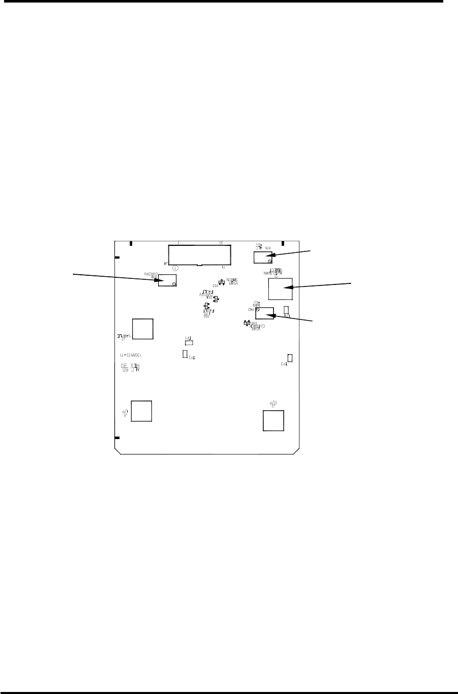
Innovator CHV0TD/RD-1 through CHV4TD/RD ATSC System Set Up Procedure
Transmitter/Regenerative Translator
Instruction Manual, Rev. 1 92
System Set Up Procedure
This system was aligned at the factory and should not require additional adjustments
to achieve normal operation.
This Innovator CX series system is of a drawer design with multiple boards inside the
drawer. If a board fails, that board needs to be changed out with a replacement
board. The failed board can then be sent back to Axcera for repair. NOTE: Contact
Axcera Customer Service Department at 1-724-873-8100 or fax to 1-724-873-8105,
before sending in any board or module.
Refer to Figure 16. Check that the Auto/Man switch S1 on the ALC Board is in the
Automatic ALC position. (NOTE: The silkscreen is incorrect on Rev. A, B & C boards.
Auto position is with the bat to the left, toward J4.) Adjust R75 the ALC pot on the
ALC Board as needed to attain 100% output power. Switch to Manual Gain (Manual
ALC) and adjust the Manual Gain pot R62 for 100% output power. Switch the ALC
Board back to Automatic ALC.
Figure 16: (A5) ALC Board (1315006 or 1308570)
S1
AUTO/MAN
J4
R75
ALC ADJ
R62
MAN ADJ
R38
OVERDRIVE
THRESHOLD
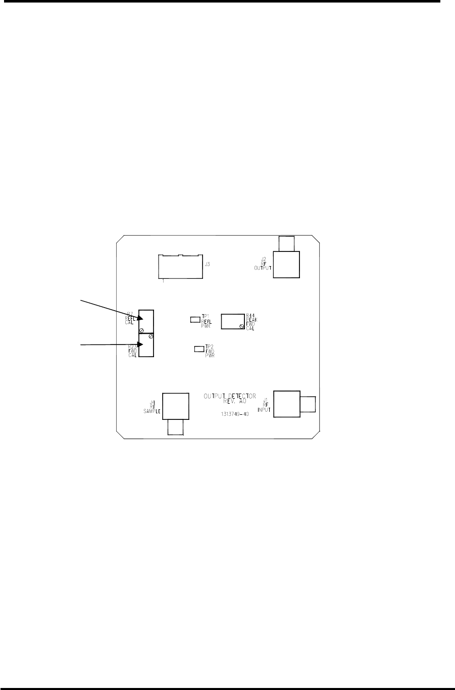
Innovator CHV0TD/RD-1 through CHV4TD/RD ATSC System Set Up Procedure
Transmitter/Regenerative Translator
Instruction Manual, Rev. 1 93
ALC Board Set-Up, Forward and Reflected Power Calibration for CHV0xD-4
systems
NOTE: If your system has one or more external amplifier drawers, refer to the next
section for the forward and reflected power calibration procedures.
Refer to Figure 16. Locate (A5) the ALC Board (1315006), in the preset the
Overdrive Threshold pot R38 full CW and set R62, Manual Adjust, and R75, ALC
Adjust, full CCW.
Switch S1 to Manual Gain, and increase the output power to 100% using R62.
Calibrate the system output power for 100% using R23, the Forward Calibration pot,
on the Output Detector Board. Refer to Figure 17.
Figure 17: (A7) Output Metering Detector Board (1313747)
R23
FORWARD
CAL ADJ
R7
REFLECTED
CAL ADJ
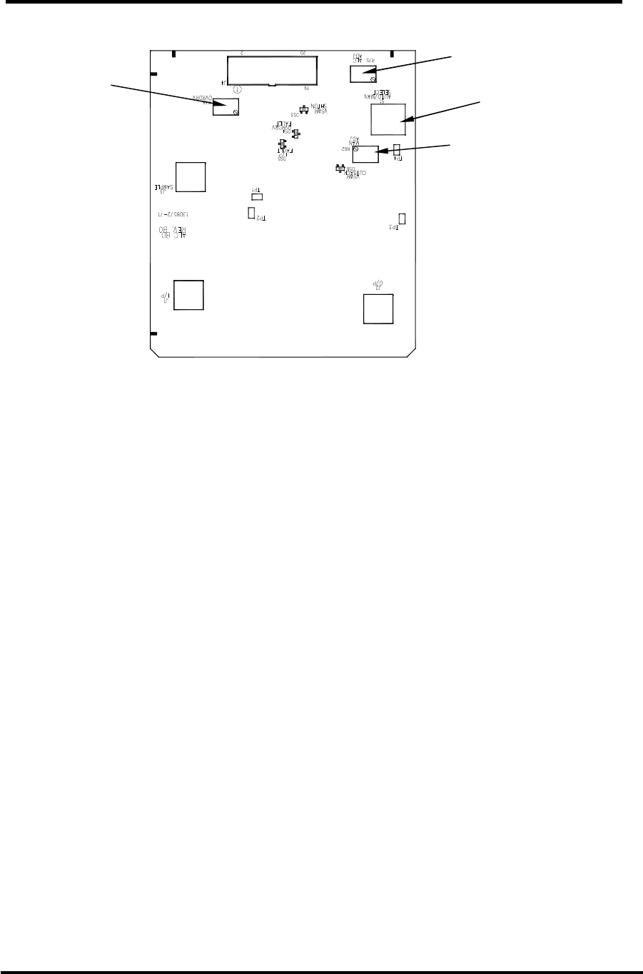
Innovator CHV0TD/RD-1 through CHV4TD/RD ATSC System Set Up Procedure
Transmitter/Regenerative Translator
Instruction Manual, Rev. 1 94
Figure 16A: (A5) ALC Board (1315006)
Refer to Figure 16A. Turn the output power down to 10% power with R62 on the
ALC Board. Remove the output RF connector from J2 on drawer and calibrate the
reflected power to 10%, using R7, the Reflected Calibration pot, on the Output
Detector Board. Refer to Figure 17. Re-connect the RF output connector to the
drawer and increase the power, in Manual gain using R62 on the ALC Board, to
115%. Adjust the Overdrive pot R38 on the ALC Board, CCW until the overdrive
threshold just trips and the Overdrive Fault LED DS4 lights. Turn R38 slightly CW so
that power comes back up and DS4 goes out.
Switch S1 on the ALC Board to ALC. Turn the ALC Adjust pot R75 on the ALC Board
until the power is 100%. Switch S1 between ALC and Manual to verify smooth
switching, with minimal change in power. If necessary repeat the above procedure.
With the drawer in ALC, use the ALC Adjust pot, R75, to decrease the power to 10%.
Remove the RF output connector from the drawer. Verify that the VSWR Cutback
LED, DS6, comes on and the Reflected Power drops to approximately 6%.
Reconnect the RF output connector and increase the power back up to 100% using
R75.
This completes the set up of the ALC board and the Forward and Reflected Power
Calibration.
Forward and Reflected Power Calibration of Systems with one or more
External Amplifier Drawers
NOTE: If your system does not contain external amplifiers, refer to the previous
section for the forward and reflected power calibration procedures.
Connect a calibrated coupler and average reading power meter to the output of the
DTV mask filter. On the ALC Board (1315006), mounted in the Driver Drawer, set
the Switch S1, Auto/Manual ALC, to the Manual position. Refer to Figure 13A.
Adjust the Manual adjustment Pot, R62, for the desired output power level as
R38
OVERDRIVE
THRESHOLD
S1
AUTO/MAN
R75
ALC ADJ
R62
MAN ADJ
J4

Innovator CHV0TD/RD-1 through CHV4TD/RD ATSC System Set Up Procedure
Transmitter/Regenerative Translator
Instruction Manual, Rev. 1 95
indicated on the average reading power meter. In the Amplifier Drawer, on the
Amplifier Control Board (1309822), refer to Figure 18; adjust the Forward Calibration
Adjustment pot, R8, for a reading of 100% on the External Amplifier Forward Power
screen of the LCD display mounted on the Driver Drawer.
Figure 18: (A5) Amplifier Control Board (1309822)
On the ALC Board mounted in the Driver Drawer, set the Switch S1, Auto/Manual
ALC, to the Auto position. Adjust the ALC adjustment Pot, R75, for a reading of
100% on the External Amplifier Forward Power screen of the LCD display mounted
on the Driver Drawer. This completes the forward power set up and calibration
adjustments.
On the ALC Board mounted in the Driver Drawer, adjust the ALC adjustment Pot,
R75, for a reading of 10% on the External Amplifier Forward Power screen of the LCD
display mounted on the Driver Drawer. Disconnect the load or the antenna
connected to the system. In the Amplifier Drawer, on the Amplifier Control Board
(1309822), adjust the Reflected Calibration Adjustment pot, R26, for a reading of
10% on the External Amplifier Reflected Forward Power screen of the LCD display
mounted on the Driver Drawer. Reconnect the load or the antenna to the system.
Adjust the ALC adjustment Pot, R75, for a reading of 100% on the External Amplifier
Forward Power screen of the LCD display mounted on the Driver Drawer. This
completes the reflected power calibration adjustment.
R8 FWD CAL ADJ
R26 REFL CAL ADJ

Innovator CHV0TD/RD-1 through CHV4TD/RD ATSC System Set Up Procedure
Transmitter/Regenerative Translator
Instruction Manual, Rev. 1 96
This page has been intentionally left blank.
APPENDIX A:
Innovator CHV0TD/RD-1 through CHV4TD/RD ATSC
Transmitter/Regenerative Translator
System and Drawer
Drawings and Parts Lists

Innovator CHV0TD/RD-1 through CHV4TD/RD ATSC Appendix A:
Transmitter/Regenerative Translator Drawings and Parts List
Instruction Manual, Rev. 1 A-1
Innovator CHV0xD VHF High Band
Regenerative Translator System and Drawer
Drawing List
Innovator CHV0xD VHF High Band Digital Regenerative Translator
(Contains a CHV0xD 20 Watt VHF High Band Digital Drawer 1313960)
CHV20BRD, Colstrip Site, Montana, Racking Plan ................................... 1316452
CHV20BRD, Montana, Rack w/110VAC Parts List .................................. CB005859
CHV20BRD, Colstrip Site, Montana, System Parts List........................... CB005862
CHV20BRD Innovator 20 Watt Digital Drawer
CHV20BRD Interconnect................................................................... 1313984
CHV20BTD/BRD Assembly Drawing ................................................... 1313960
CHV20BRD Typical Parts List............................................................. 1313960
CHV20BRD, Montana, Parts List ...................................................... CB005860