UBS Axcera CU150BTD 150-Watt UHF Digital Transmitter User Manual axciter Master 3 22 07
UBS-Axcera 150-Watt UHF Digital Transmitter axciter Master 3 22 07
Contents
- 1. User manual 1
- 2. User manual 2
- 3. User manual 3
- 4. User manual 4
- 5. User manual 5
User manual 3
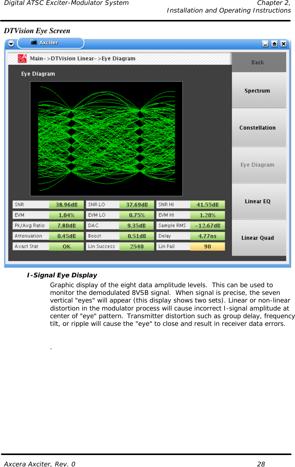
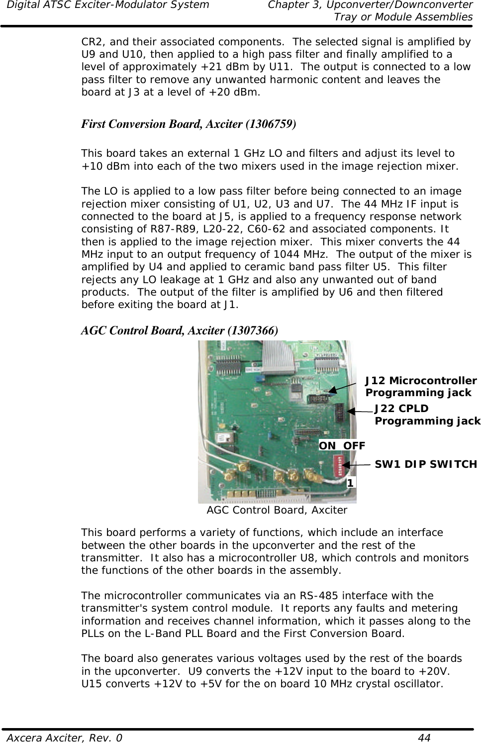
![Digital ATSC Exciter-Modulator System Appendix D: Glossary Axcera Axciter, Rev. 0 D-1 Appendix D: Glossary of Terms Acronyms Definitions 1x clock 10.762238 MHz symbol clock 8x clock 86.097902 MHz clock AEQ Adaptive Equalizer AES Audio Engineering Society (standard for digital audio) AES/EBU Audio Engineering Society/European Broadcasting Union (standard for digital audio) AFC Automatic Frequency Control ALC Automatic Level Control Alias A false signal from beats between signal frequency and sampling frequency API Application Program Interface ATSC Advanced Television Systems Committee / Digital TV / DTV Aural Analog television sound signal AVGNL Averaging of nonlinear equalizers BEQ Baseband equalizer Channel Coder PC board that accepts SMPTE data and produces clock signals and ATSC-compliant symbols Combiner Notch diplexer for combining separately amplified NTSC visual and aural signals dB Decibel measurement of a power. 10 * log (base 10) of the power ratio. dBm Decibel measurement with respect to 1milliWatt. Measurement of power. DDS Int 32 bit – Direct Digital Synthesizer – generates a frequency DSB Double Side Band DTV Digital Television DTVAEQ Digital Television Adaptive [linear] Equalizer EDH Error Detection and Handling EVM Error Vector Magnitude – measured in percentage FCC Federal Communications Commission FPGA Field Programmable Gate Array Ideali Ideal I (in-phase) channel signal Idealq Ideal Q (quadrature) channel signal IEQ Integer Equalizer IF Intermediate Frequency](https://usermanual.wiki/UBS-Axcera/CU150BTD.User-manual-3/User-Guide-1145891-Page-28.png)