UBS Axcera DT835A-6 3000-Watt UHF DTV Transmitter User Manual DM8 R Modulator Instruction Manual
UBS-Axcera 3000-Watt UHF DTV Transmitter DM8 R Modulator Instruction Manual
Contents
- 1. Compiled Transmitter User Manual
- 2. Compiled DM8 Tray Manual
Compiled DM8 Tray Manual

Instruction Manual
DM8-R
Digital Modulator Tray
AXCERA, LLC
103 FREEDOM DRIVE, P.O. Box 525 LAWRENCE, PA 15055-0525 USA
(724) 873-8100 • FAX (724) 873-8105
www.axcera.com • info@axcera.com

DM8-R Digital Modulator Tray Table of Contents
DM8-R Digital Modulator, Rev. 0 1
DM8-R DIGITAL MODULATOR TABLE OF CONTENTS
SECTION...................................................................................................PAGE
Overview ......................................................................................................2
Inputs and Outputs ........................................................................................2
Front Panel Interface......................................................................................2
DM8-R Modulator Board Configuration..............................................................3
Detailed Circuit Descriptions............................................................................3
DM8-R Modulator Board Description..............................................................3
SMPTE-310 Input.....................................................................................3
Channel Coder.........................................................................................3
Analog Output Section .............................................................................4
Pilot Frequency Generation.......................................................................4
DM8-R Front Panel Board Description............................................................4
Initial Setup ..................................................................................................5
Drawing List ..................................................................................................6
DM8-R Digital Modulator Tray Tray Description
DM8-R Digital Modulator, Rev. 0 2
DM8-R Modulator Tray
Overview
The DM8-R modulator Tray is an ATSC compliant 8 VSB modulator that mounts in a
standard 19” rack. The DM8-R modulator accepts a SMPTE-310 MPEG data stream and
outputs a 6 MHz wide IF output centered at 44 MHz with a pilot carrier at 46.69 MHz.
The DM8-R modulator provides linear and nonlinear correction capability for the
transmission path as well as internal test sources that are used during initial transmitter
installation. All of the functions of the DM8-R modulator are controlled from the LX
Controller LCD display and pushbuttons.
Inputs and Outputs
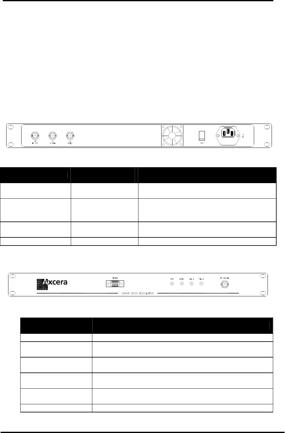
The inputs and outputs of the DM8-R modulator are described in the table below.
Description Reference
Designator Function
IF Output J4 Provides a 44 MHz IF Output with a 50
ohm output impedance
10 MHz Input J3 10 MHz input to the DM8-R modulator.
Provides the reference frequency to the
pilot VCXO.
SMPTE-310M Input J2 SMPTE-310 input that provides the MPEG
stream to the modulator.
110/220 VAC J1 Input Power to the Modulator
Front Panel Interface
The following table describes the connectors and indicators on the front panel.
LED Indicator or
Connector Function
PWR Indicates that the DC power supply is operating
MPEG
LED Indicates the presence of a valid MPEG stream at the
J1-2B input
PLL A
LED Indicates that the DM8 symbol clock is locked to the
frequency of the 10 MHz reference.
PLL B
LED Indicates that the pilot frequency is locked to the
incoming 10 MHz reference.
IF Sample Jack
BNC Provides a sample of the IF output from the modulator
at approximately a –20 dBm level.
RS-232 SERIAL Serial Port used for initial modulator alignment

DM8-R Digital Modulator Tray Board Descriptions
DM8-R Digital Modulator, Rev. 0 3
DM8-R Modulator Board Configuration
The Digital Modulator Board in the DM8-R is setup through a configuration header
located on the board. The configuration header contains 8 jumper positions between
pins on J26 and J27. The functions of these positions are given in Table 1.
Table 1 J26/J27 Configuration Header Definition
Function when
Jumper Position Jumper Is Present Jumper Not Present
1 Header Enabled RS485 Enabled
2 CW Zero Normal Mode
3 Internal PRBS External Source
4 Linear Equalizer On Linear Equalizer Off
5 Nonlinear Off Nonlinear On
6 Preset Table 1 Preset Table 2
7 AGC Tracking AGC Fixed
8 Spare
Detailed Circuit Descriptions
Digital Modulator Board (1304884)
SMPTE-310 Input
The DM8-R modulator accepts a SMPTE-310 input the BNC Jack J2 located on the rear
panel of the tray. This input is connected to J42 on the Digital Modulator Board via a
RG-179 cable. This input is applied to a high speed window comparator that adjusts the
level to a low voltage TTL signal to be used by the Altera FPGA, U3. The SMPTE-310
signal is input to the FPGA to recover the clock and the data. A portion of the clock and
recovery circuit is performed by a high speed comparator, U17, that functions as an
external delay circuit.
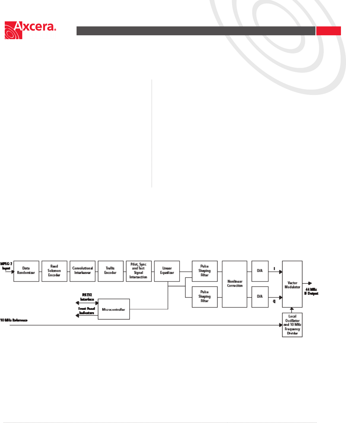
Channel Coder
The FPGA subsequently uses the SMPTE-310 clock and data as the input to the channel
coder contained inside the FPGA. The channel coder is a series of DSP blocks defined by
the ATSC standard for 8 VSB data transmission. These blocks include the data
randomizer, Reed Solomon Encoder, data interleaver, trellis coder, and sync insertion.
The channel coder portion inside the FPGA generates the 8 distinct levels in an 8 VSB
transmitter. These levels are subsequently input to a linear equalizer that provides for
frequency response correction in the transmission path. The linear equalizer is a 67 tap
FIR filter that is loaded with tap values from the microntroller, U1, located on this board.
The output of the linear equalizer is then input to two pulse shaping filters, an in phase
(I) and a quadrature (Q) filter that are also located inside the FPGA. The pulse shaping
filters are FIR filters that have fixed tap values that are preset inside the FPGA. The
output of the pulse shaping filters is then applied to a Pre-Distortion Linearizer chip, U4,
which can be used to correct for nonlinearities in the data transmission path. The
output of the Pre-Distortion chip is gain scaled and output to a dual D/A converter that
output a baseband I and Q analog signal.

DM8-R Digital Modulator Tray Board Descriptions
DM8-R Digital Modulator, Rev. 0 4
Analog Output Section
The baseband I and Q signals from the D/A converter are applied to differential analog
filters that remove some of digital artifacts from the D/A conversion process. The output
of the I channel filter is then mixed with the pilot frequency, 46.69 MHz, using mixer
U30. The output of the Q filter is mixed with the pilot frequency that is phase shifted 90
degrees using mixer U34. The mixers are current driven devices so that when the
outputs of U30 and U34 are connected together, they provide a combined output. This
combined output is subsequently input to a final differential output filter which provides
the final IF output at the SMA connector, J38. This output is connected through a RG-
174 cable to the BNC connector J4, the IF output jack, located on the rear panel of the
tray.
Pilot Frequency Generation
The 46.69 MHz pilot signal, which is used in the mixing process, is generated from a
46.69 MHz VCXO that is phase locked to a 10 MHz reference. The VCXO and the 10 MHz
are divided down to a common frequency, which is then compared internal to the FPGA.
The FPGA subsequently provides error signals to a analog phase locked implemented
with op amp stages U45-A, B and C. The output of these compensation stages is used
as the control voltage to the VCXO, U37. The phase locked output of U37 is applied to
a analog filter to remove harmonics of the pilot and then input to quadrature splitter Z1.
The outputs of Z1 are used as the inputs to the mixers in the analog output section.
DM8-R Front Panel Board (1307113)
The front panel board contains four LEDs, Power, MPEG, PLL A and PLL B, which are
viewable on the front panel. J2 connects to the Modulator Board, which controls the
operation of the LEDs. When the system is operation normally, all LEDs will be Green.
If a problem occurs, that LED will not be lit.

DM8-R Digital Modulator Tray Initial Set Up
DM8-R Digital Modulator, Rev. 0 5
Initial Set Up
The DM8-R Modulator Tray was set up at the factory for best digital response and
correction for the transmitter and should require no customer adjustments to attain
normal operation.
The digital transmitter operates using an MPEG input that connects to J2 on the rear of the
DM8-R Modulator Tray. The IF output of the DM8-R Modulator Tray, at J4, connects to the
IF input jack located on the exciter for the transmitter. The transmitter is ready for
normal operation. Refer to the instruction manual for the transmitter for information on
the transmitter setup and operation.
If a problem occurred during the setup of the transmitter, help can be found by calling
Axcera field support at 724-873-8100.

DM8-R Digital Modulator Tray Drawing List
DM8-R Digital Modulator, Rev. 0 6
DM8-R Modulator Tray
Interconnect.......................................................................................1306984
Digital Modulator, DT1D Board
Schematic..........................................................................................1304884
DM8-R Front Panel Board
Schematic..........................................................................................1307113
8-VSB Modulator - DM8-R
The DM8-R 8-VSB modulator accepts an ATSC-compliant SMPTE 310M
digital bit stream. To modulate to the 8-VSB standard, the digital data
stream is first randomized and then forward error corrected (FEC)
through Reed-Solomon encoding, data field interleaving and trellis
coding. The FEC signal processing minimizes data errors in the digital
bit stream and reduces the chance of burst errors, while significantly
improving the system coding gain. The data is then equalized,
processed through pulse shaping filters and modulated to the 8-VSB
signal (centered at 44 MHz) utilizing Quadrature Vector Modulation
techniques. A crystal controlled oscillator provides excellent stability
and performance.
Front panel LEDs provide a quick indication of operating status and
performance of the modulator. In addition, a 9-pin serial port is provided
for the configuration of the digital linear and nonlinear pre-correctors.
Specifications published here are current as of the date of publication of this document. Because we are continuously improving our products, Axcera reserves the right to change specifications without prior
notice. At any time, you may verify product specifications by contacting our office. Axcera views it’s patent portfolio as an important corporate asset and vigorously enforces its patents. Products or features
contained herein may be covered by one or more U.S. or foreign patents.
0608R0 © 2006 AXCERA All Rights Reserved An Equal Opportunity Employer
103 Freedom Drive, PO Box 525, Lawrence, PA 15055 t: 724-873-8100 f:724-873-8105 www.axcera.com
General
Modulation Type 8-VSB
Symbol Rate 10.76 MHz
Error Protection (Per ATSC Standard) RS(207, 187) t=10
Convolutional Interleaver
2/3 Rate Trellis Encoder
Signal to Noise Ratio (SNR) 34 dB min (36 dB typical)
Out of Band Rejection 41 dB min (47 dB typical)
EVM 2.0% max (1.5% typical)
Data Interface
Data Rate (MPEG-2) 19.39 Mbps, 6 MHz channel
Interface SMPTE 310M
IF Output
Frequency 44 MHz IF, 6 MHz channel
Impedence 50 Ohms
Level -6 dBm
Mechanical
Size (W x D x H) 19” x 12” x 1.75”
Weight 6 lbs
Power Requirements
Line Voltage 84 to 264 VAC,
1 phase 50/60 Hz
Power Consumption 50W
Test Signal Capabilities
Mpeg Source Internal PRBS-23
Test Waveforms Zero Pilot
8-VSB Modulator - DM8-R