UBS Axcera DT835A-6 3000-Watt UHF DTV Transmitter User Manual title page DT835A
UBS-Axcera 3000-Watt UHF DTV Transmitter title page DT835A
Contents
- 1. Compiled Transmitter User Manual
- 2. Compiled DM8 Tray Manual
Compiled Transmitter User Manual

INSTRUCTION MANUAL
DT835A
DIGITAL
UHF TRANSMITTER
AXCERA, LLC
103 FREEDOM DRIVE P.O. BOX 525 LAWRENCE, PA 15055-0525 USA
(724) 873-8100 • FAX (724) 873-8105
www.axcera.com • info@axcera.com

Digital UHF Transmitter Table of Contents
DT835A, Rev. 1 i July 23, 2003
TABLE OF CONTENTS
CHAPTER 1 INTRODUCTION
Section Page
1.1 Manual Overview..................................................................................1-1
1.2 Safety.................................................................................................1-1
1.3 Maintenance ........................................................................................1-2
1.4 Material Return Procedure .....................................................................1-2
1.5 Limited One-Year Warranty for Axcera Products.......................................1-3
CHAPTER 2 SYSTEM DESCRIPTION AND CUSTOMER REMOTE CONNECTIONS
2.1 System Overview .................................................................................2-1
2.1.1 Single UHF Exciter Assembly ........................................................2-1
2.1.2 (Optional) 10 MHz Reference Distribution Amplifier Tray..................2-2
2.1.3 DM8-R Modulator Tray.................................................................2-2
2.1.4 Amplifier Array Assemblies...........................................................2-2
2.1.5 Transmitter Output Assemblies.....................................................2-3
2.1.6 Control and Status ......................................................................2-3
2.1.7 Metering Panel............................................................................2-4
2.1.8 UHF Exciter Tray .........................................................................2-5
2.1.9 Variable Gain/Phase Tray .............................................................2-6
2.1.10 UHF Amplifier Tray .....................................................................2-6
2.1.11 Modulator front panel menus and indicators ..................................2-7
2.1.12 Main AC Input............................................................................2-8
2.1.13 Customer Remote Interface Connections.............................. 2-8
CHAPTER 3 INSTALLATION AND SETUP PROCEDURES
3.1 Site Considerations................................................................................3-1
3.2 Unpacking the Cabinets and Trays...........................................................3-4
3.3 Installing the Cabinets and Trays ............................................................3-4
3.3.1 DM8-R Modulator Installation ........................................................3-5
3.4 Main AC Inputs......................................................................................3-6
3.5 Output Connections...............................................................................3-6
3.6 Setup and Operation Procedures.............................................................3-7
3.6.1 DM8-R Modulator Setup Procedures ...............................................3-8
CHAPTER 4 CIRCUIT DESCRIPTIONS
4.1 UHF Exciter Assembly ............................................................................4-1
4.1.1 Control and Status .......................................................................4-1
4.1.2 Digital Input and Remote Connections............................................4-1
4.1.3 AC Input .....................................................................................4-2
4.2 DM8-R Modulator Tray...........................................................................4-2
4.2.1 DM8 Digital Modulator Board .........................................................4-2
4.2.2 DM8-R Front Panel Board..............................................................4-3
4.3 UHF Exciter Tray ..................................................................................4-3
4.3.1 UHF Filter...................................................................................4-3
4.3.2 UHF Generator Board...................................................................4-4
4.3.3 (Optional) 10-MHz Reference Oscillator Board ................................4-4

Digital UHF Transmitter Table of Contents
DT835A, Rev. 1 ii July 23, 2003
TABLE OF CONTENTS
CHAPTER 4 CIRCUIT DESCRIPTIONS - Continued
Section Page
4.3.4 PLL Board...................................................................................4-5
4.3.5 Power Entry Module.....................................................................4-7
4.3.6 IF Phase Corrector Board .............................................................4-7
4.3.7 ALC Board ..................................................................................4-9
4.3.8 Visual/Aural Metering Board .......................................................4-15
4.3.9 UHF Upconverter Board..............................................................4-16
4.3.10 Transmitter Control Board .........................................................4-17
4.3.11 +12V(4A)/-12V(1A) Power Supply Board....................................4-22
4.3.12 5-Section Delay Equalizer Board ................................................4-23
4.4 Variable Phase/Gain Tray ....................................................................4-23
4.4.1 Variable Gain/Phase Board ..........................................................4-23
4.4.2 Metering Board ..........................................................................4-24
4.4.3 Power Entry Module....................................................................4-24
4.4.4 +15V/-12V Power Supply Board ..................................................4-24
4.5 Metering Panel ...................................................................................4-24
4.5.1 Splitter Board ............................................................................4-25
4.5.2 Visual/Aural Metering Board ........................................................4-25
4.5.3 Dual Peak Detectors ...................................................................4-25
4.5.4 Detector Threshold Board............................................................4-26
4.5.5 Power Entry Module....................................................................4-26
4.5.6 +/-12V Power Supply Board........................................................4-26
4.6 AC Distribution Assembly, UHF Exciter..................................................4-27
4.7 2-3kW Amplifier Array.........................................................................4-27
4.8 UHF Amplifier Trays............................................................................4-29
4.8.1 UHF Filter.................................................................................4-29
4.8.2 1-Watt Amplifier Board Assembly................................................4-29
4.8.3 1-Watt Amplifier Board ..............................................................4-30
4.8.4 Single Stage Amplifier Assembly.................................................4-30
4.8.5 Coupler Board...........................................................................4-34
4.8.6 Dual Peak Detector Enclosure.....................................................4-34
4.8.7 Dual Peak Detector Board ..........................................................4-34
4.8.8 4-Way Splitter Assembly............................................................4-35
4.8.9 4-Way Splitter Board .................................................................4-35
4.8.10 Dual Stage Amplifier Assembly...................................................4-35
4.8.11 Amplifier Protection Board .........................................................4-39
4.8.12 Amplifier Control Board.............................................................4-40
4.8.13 Variable Gain/Phase Enclosure...................................................4-42
4.8.14 Variable Gain/Phase Board ........................................................4-42
4.8.15 4-Way Combiner Assembly........................................................4-43
4.9 AC Distribution Assembly, Single Phase Amplifier Array..........................4-44
4.10 AC Distribution Assembly, Three Phase Amplifier Array..........................4-45
4.11 Combiner Reject Load Assembly..........................................................4-45
4.11.1 Combiner Reject Load Board......................................................4-46

Digital UHF Transmitter Table of Contents
DT835A, Rev. 1 iii July 23, 2003
TABLE OF CONTENTS - (continued)
Section Page
CHAPTER 5 DETAILED ALIGNMENT PROCEDURES
5.1 DM8-R Modulator ..................................................................................5-1
5.1.1 DM8-R Modulator Board Configuration .........................................5-1
5.2 UHF Exciter Tray ...................................................................................5-2
5.2.1 Delay Equalization Adjustment......................................................5-3
5.2.2 IF Phase Corrector Adjustment .....................................................5-3
5.2.3 UHF Generator Board...................................................................5-3
5.2.4 10-MHz Reference Generator Board ..............................................5-4
5.2.5 PLL Board...................................................................................5-4
5.3 UHF Amplifier Trays...............................................................................5-4
5.3.1 Variable Gain/Phase Board ...........................................................5-4
5.3.2 1-Watt UHF Amplifier Board .........................................................5-4
5.3.3 UHF Filter...................................................................................5-4
5.3.4 Single Stage Amplifier Assembly...................................................5-4
5.3.5 Coupler Board.............................................................................5-4
5.3.6 Dual Stage Amplifier Assembly .....................................................5-5
5.3.7 4-Way Splitter Assembly..............................................................5-5
5.3.8 Dual Stage Amplifier Assembly .....................................................5-5
5.3.9 4-Way Combiner Assembly...........................................................5-6
5.3.10 Circulator...................................................................................5-6
5.3.11 Dual Peak Detector Board............................................................5-6
5.3.12 Amplifier Protection Board ...........................................................5-6
5.3.13 Amplifier Control Board...............................................................5-6
5.3.14 Switching Power Supply ..............................................................5-6
5.3.15 Calibration of Output and Reflected Power and VSWR Cutback ........5-6
5.4 Phase and Gain Adjustment of the UHF Amplifier Trays in each Array..........5-7
5.5 Calibration of the Side A and Side B Arrays Forward Output Power .............5-7
5.6 Calibration of the Side A and Side B Arrays Reflected Output Power............5-7
5.7 Phase and Gain Adjustment for the entire Amplifier Array..........................5-8
5.8 Calibration of the Forward Output Power Level of the Transmitter...............5-8
5.9 Calibration of the Reflected Output Power Level of the Transmitter .............5-8
5.10 Calibration of the Reject Output Power Level of the Transmitter................5-9
APPENDICES
APPENDIX A SAMPLE LOG REPORT SHEET
APPENDIX B TYPICAL OPERATIONAL READINGS
APPENDIX C ASSEMBLY DRAWINGS AND PARTS LISTS
APPENDIX D SUBASSEMBLY DRAWINGS AND PARTS LISTS
APPENDIX E DT835A SYSTEM SPECIFICATIONS

Digital UHF Transmitter Table of Contents
DT835A, Rev. 1 iv July 23, 2003
LIST OF FIGURES
2-1 Exciter Remote Interface Assembly ................................................2-10
2-2 Amplifier Array Remote Interface Panel ..........................................2-14
3-1 1 kW Minimum Ventilation Configuration...........................................3-4
3-2 Tray Installation Instructions...........................................................3-6
5-1 Typical Digital Spectrum ...............................................................5-12

Digital UHF Transmitter Table of Contents
DT835A, Rev. 1 v July 23, 2003
LIST OF TABLES
2-1 DT835A Major Assemblies ...............................................................2-1
2-2 Metering Panel Meters.....................................................................2-4
2-3 UHF Exciter Tray Meters..................................................................2-5
2-4 UHF Exciter Tray Switches...............................................................2-5
2-5 UHF Exciter Tray Fault Indicators.....................................................2-5
2-6 UHF Exciter Tray Samples ...............................................................2-6
2-7 Variable Phase/Gain Tray Meters......................................................2-6
2-8 Variable Phase/Gain Tray Sample.....................................................2-6
2-9 UHF Amplifier Tray Meters...............................................................2-6
2-10 UHF Amplifier Tray Status Indicators................................................2-7
2-11 UHF Amplifier Tray Control Adjustments ...........................................2-7
2-12 UHF Amplifier Tray Sample..............................................................2-7
2-13 Modulator Front Panel LEDs.............................................................2-8
2-14 Customer Remote Control Interface Connections.................... 2-12
3-1 MPEG and 10 MHz Input Information................................................3-6
3-2 Jumper Positions in the Gain 1 and Gain 2 Circuits
For an Input Level of Between –6 and –26 dBm.................................3-8
4-1 Fuses, Idling Currents and Voltage Settings for Amplifier Devices......4-42
5-1 8-VSB Modulator Connections..........................................................5-1
5-2 Jumper Configurations for the Symbol Generator Board......................5-3
5-3 Jumper Configurations for the VSB Filter Board .................................5-5
5-4 DIP Switch Settings........................................................................5-6
5-5 Jumper Positions on the 6 dB Pad ..................................................5-10
5-6 Center Frequencies for the Delay Equalizer Sections.........................5-11
5-7 PLL Board Switch Positions............................................................5-13
5-8 Switch Positions for Channel Frequencies........................................5-14

Digital UHF Transmitter Chapter 1, Introduction
DT835A, Rev. 1 1-1
Chapter 1
Introduction
This manual explains the installation,
setup, alignment, and maintenance
procedures for the DT835A Digital UHF
Transmitter. It is important that you
read all of the instructions, especially
the safety information in this chapter,
before you begin to install or operate
the unit.
1.1 Manual Overview
This instruction manual is divided into
four chapters and supporting appendices.
Chapter 1, Introduction, contains
information on safety, maintenance,
return procedures, and warranties. The
Chapter 2, System Description and
Customer Remote Interface Connections,
describes the transmitter and includes
discussions of system control and status
indicators and remote control
connections. Chapter 3, Installation and
Set up Procedures, explains how to
unpack, install, setup, and operate the
transmitter. Chapter 4, Circuit
Descriptions, provides information on the
boards and subassemblies that make up
the DT835A. Chapter 5, Detailed
Alignment Procedures, provides
information on adjusting the system
assemblies for optimal operation The
appendices contain sample log sheets,
typical operational readings, assembly
and subassembly drawings and parts list,
and system specifications.
1.2 Safety
The digital UHF transmitters
manufactured by Axcera are designed for
ease of use and repair while providing
protection from electrical and mechanical
hazards. Listed throughout the manual
are notes, cautions, and warnings
concerning possible safety hazards that
may be encountered while operating or
servicing the transmitter. Please review
these warnings and familiarize yourself
with the operation and servicing
procedures before working on the
transmitter.
Read All Instructions – All of the
operating and safety instructions should
be read and understood before operating
this equipment.
Retain Manuals – The manuals for the
transmitter should be retained at the
transmitter site for future reference. We
provide two sets of manuals for this
purpose; one set can be left at the office
while one set can be kept at the site.
Heed Notes, Warnings, and
Cautions – All of the notes, warnings,
and cautions listed in this safety section
and throughout the manual must be
followed.
Follow Instructions – All of the
operating and use instructions for the
transmitter should be followed.
Cleaning – Unplug or otherwise
disconnect power from the equipment
before cleaning. Do not use liquid or
aerosol cleaners. Use a damp cloth for
cleaning.
Ventilation – Openings in the cabinets
and tray front panels are provided for
ventilation. To ensure reliable operation,
and to protect the unit from overheating,
these openings must not be blocked.
Servicing – Do not attempt to service
this product yourself until becoming
familiar with the equipment. If in doubt,
refer all servicing questions to qualified
Axcera service personnel.
Replacement Parts – When
replacement parts are used, be sure that
the parts have the same functional and
performance characteristics as the
original part. Unauthorized substitutions
may result in fire, electric shock, or other

Digital UHF Transmitter Chapter 1, Introduction
DT835A, Rev. 1 1-2
hazards. Please contact the Axcera
Technical Service Department if you have
any questions regarding service or
replacement parts.
1.3 Maintenance
The DT835A is designed with
components that require little or no
periodic maintenance except for the
routine cleaning of the fans and the front
panels of the trays.
The amount of time between cleanings
depends on the conditions within the
transmitter room. While the electronics
have been designed to function even if
covered with dust, a heavy buildup of
dust, dirt, or insects will affect the
cooling of the components. This could
lead to a thermal shutdown or premature
failure of the affected trays.
When the front panels of the trays
become dust covered, the top covers
should be removed and any accumulated
foreign material removed. A vacuum
cleaner, utilizing a small wand-type
attachment, is an excellent way to
suction out the dirt. Alcohol and other
cleaning agents should not be used
unless you are certain that the solvents
will not damage components or the silk-
screened markings on the trays and
boards. Water-based cleaners can be
used, but do not saturate the
components. The fans and heatsinks
should be cleaned of all dust or dirt to
permit the free flow of air for cooling
purposes.
It is recommended that the operating
parameters of the transmitter be
recorded from the meters on the trays
and the system metering control panel at
least once a month. It is suggested that
this data be retained in a rugged folder
or envelope. A sample format for a log
sheet is provided in Appendix A.
Photocopies of the log sheet should be
made for continued data entries.
1.4 Material Return Procedure
To insure the efficient handling of
equipment or components that have been
returned for repair, Axcera requests that
each returned item be accompanied by a
Material Return Authorization Number
(MRA#).
An MRA# can be obtained from any
Axcera Field Service Engineer by calling
the Axcera Field Service Department, at
(724) 873-8100. This procedure applies
to all items sent to the Field Service
Department regardless of whether the
item was originally manufactured by
Axcera.
When equipment is sent to the field on
loan, an MRA# is included with the unit.
The MRA# is intended to be used for the
return of the unit to Axcera. In addition,
all shipping material should be retained
for the return of the unit to Axcera.
Replacement assemblies are also sent
with an MRA# to allow for the proper
routing of the exchanged hardware.
Failure to close out this type of MRA# will
normally result in invoicing for the value
of the loaner item or the exchange
assembly.
When shipping an item to Axcera, please
include the MRA# on the packing list and
on the shipping container. The packing
slip should also include contact
information and a brief description of why
the unit is being returned.
Please forward all MRA items to:
Axcera
103 Freedom Drive
P.O. Box 525
Lawrence, PA 15055-0525 USA
For more information concerning this
procedure, call the Axcera Field Service
Department, at (724) 873-8100 or by
fax at (724) 873-8105.
Axcera can also be contacted through e-
mail at service@axcera.com and on the
Web at www.axcera.com.

Digital UHF Transmitter Chapter 1, Introduction
DT835A, Rev. 1 1-3
1.5 Limited One-Year Warranty for
Axcera Products
Axcera warrants each new product that
it has manufactured and sold against
defects in material and workmanship
under normal use and service for a
period of one (1) year from the date of
shipment from Axcera's plant, when
operated in accordance with Axcera's
operating instructions. This warranty
shall not apply to tubes, fuses,
batteries, or bulbs.
Warranties are valid only when and if
(a) Axcera receives prompt written
notice of breach within the period of
warranty, (b) the defective product is
properly packed and returned by the
buyer (transportation and insurance
prepaid), and (c) Axcera determines, in
its sole judgment, that the product is
defective and not subject to any misuse,
neglect, improper installation,
negligence, accident, or (unless
authorized in writing by Axcera) repair
or alteration. Axcera’s exclusive liability
for any personal and/or property
damage (including direct, consequential,
or incidental) caused by the breach of
any or all warranties, shall be limited to
the following: (a) repairing or replacing
(in Axcera’s sole discretion) any
defective parts free of charge (F.O.B.
Axcera’s plant) and/or (b) crediting (in
Axcera’s sole discretion) all or a portion
of the purchase price to the buyer.
Equipment furnished by Axcera, but not
bearing its trade name, shall bear no
warranties other than the special hours-
of-use or other warranties extended by
or enforceable against the manufacturer
at the time of delivery to the buyer.
NO WARRANTIES, WHETHER
STATUTORY, EXPRESSED, OR
IMPLIED, AND NO WARRANTIES OF
MERCHANTABILITY, FITNESS FOR
ANY PARTICULAR PURPOSE, OR
FREEDOM FROM INFRINGEMENT,
OR THE LIKE, OTHER THAN AS
SPECIFIED IN PATENT LIABILITY
ARTICLES, AND IN THIS ARTICLE,
SHALL APPLY TO THE EQUIPMENT
FURNISHED HEREUNDER.

Digital UHF Transmitter Chapter 2, System Description and
Customer Remote Connections
DT835A, Rev. 1 2-1
Chapter 2
System Description and Customer Remote Connections
MAJOR ASSEMBLY NUMBER TRAY/ASSEMBLY NAME
A1 Single UHF exciter assembly
A2 and A3 two 2-3kW amplifier array assemblies
A4 Hybrid combiner assembly
A7 Directional coupler assembly
Output coupler assembly
DM8-R digital modulator tray
Table 2-1: DT835A Major Assemblies
2.1 System Overview
The DT835A is a complete UHF solid-
state television transmitter that operates
at an output power of 2000 watts to
3000 watts digital, depending on the
digital application. The DT835A is made
up of three cabinets: a UHF exciter
cabinet and two amplifier array cabinets.
The DT835A is made up of the trays and
assemblies shown in Table 2-1.
2.1.1 (A1) Single UHF Exciter
Assembly
The single UHF exciter assembly
contains (A1) a UHF exciter tray, a DM8-
R digital modulator tray, (A10) an
(Optional) 10 MHz reference generator
tray, (A3) a splitter, (A4 and A5) two
variable phase/gain trays, (A6) a
metering panel, (A8) an AC distribution
assembly, and (A9) a remote interface
assembly.
The DM8-R modulator tray can have an
external 10 MHz reference connected to
J3 on the rear panel or it will generate
and internal 10 MHz reference if no
external reference is supplied. The
Digital input connects to J2 on the
remote interface assembly that is cabled
to J2 on the DM8-R modulator. The
Output from the DM8-R modulator at J4
connects to J6 on the rear of the UHF
exciter tray. The Digital IF is wired to
J18 on the 5 section delay equalizer
board, 44 MHz (1072090). The
processed digital IF signal is then cabled
to the J32 on the ALC board (1265-
1305). The digital IF input must be
selected as the input. This is
accomplished by connecting the jumper
W11 on J29 between pins 2 and 3 on the
ALC board. The digital IF is wired
through the K3 and K4 relays to the rest
of the ALC board. The LED DS5, digital
IF modulator enable, should be lit. The
ALC board has the capability of
switching between two different IF
inputs, but in this case only the digital IF
input is used.
The output of the ALC board (-10 dBm)
connects to (A11) the UHF upconverter
board (1265-1310) in the upconverter
section of the UHF digital exciter. The
upconverter takes the LO and
heterodynes it with the IF; the signal is
then filtered to produce the RF on-
channel output.
The (A15-A1) UHF generator board
(1565-1109) is mounted in the UHF
Generator Enclosure (1519-1144) for EMI
and RFI protection. The board contains a
VCXO circuit and additional circuitry to
multiply the VCXO frequency by eight.
The output is split and provides an input
to the x8 multiplier circuitry as well as a
sample for the PLL board. The amplified
eighth harmonic is then fed to the SMA
output jack of the board at J3. Typical
output level of the signal is +16 dBm
nominal.
The (Optional) (A14-A1) 10-MHz
reference generator board (1519-1126)

Digital UHF Transmitter Chapter 2, System Description and
Customer Remote Connections
DT835A, Rev. 1 2-2
is located in the (Optional) (A10) 10-MHz
reference kit (1286-1108). The board
contains a high-stability crystal oscillator
that provides a 10-MHz output that is
used as reference frequency for the
transmitter. The board is mounted within
an enclosed assembly that helps to
maintain the operating temperature of
the oscillator board.
The (A13) PLL board (1286-1104) is part
of the phase lock loop (PLL) circuit, which
provides the automatic frequency control
(AFC) voltage, that connects to the VCXO
assembly, on the UHF Generator board,
and maintains the accurate output
frequency of the VCXO. The AFC is
generated by comparing a sample of the
10-MHz reference to a sample of the
VCXO frequency. The PLL board uses an
external 10-MHz signal as the reference
unless it is missing, then an internally
generated 10-MHz signal is used. A
sample of the signal from the UHF
generator board connects to SMA jack J9,
the sample input on the board. The signal
is amplified by U8 and coupled to U9, a
divide by 20/21 IC. A sample of the
signal at the output of U8 is connected to
J10, the sample output jack on the
board, which is typically connected to the
front panel of the tray.
The selected 10-MHz reference connects
to amplifier IC U1 whose output is split.
A sample of the 10-MHz reference is
cabled to jack J3, the 10-MHz output
jack, which is connected to J5 on the rear
of the tray.
If the 50 kHz from the 10-MHz reference
and the 50-kHz from the UHF generator
board become unlocked, the red Unlock
LED, lights and the Lock LED, located on
the LED display board, is extinguished.
The RF output of the UHF exciter at J15
is split two ways by the (A3) splitter.
The RF output #1 connects to the input
of (A4) one of the variable phase/gain
trays and the RF output #2 connects to
the input of (A5) the other variable
phase/gain tray. The output of the (A4)
variable phase/gain tray connects to
(A2) the side A amplifier array
assembly. The output of the (A5)
variable phase/gain tray connects to
(A3) the side B amplifier array
assembly.
2.1.2 (Optional) 10 MHz Reference
Distribution Amplifier Tray
The (Optional) 10 MHz reference
distribution amplifier tray provides a 10
MHz reference at a suitable output level
for distribution.
The system is made up of an internal 10
MHz reference source, a reference
distribution amplifier, and splitter kit(s)
without precise offset IF to distribute the
reference signal to each transmitter.
The reference distribution amplifier tray
utilizes an internal 10 MHz reference
generator assembly to generate a 10
MHz reference signal. This signal is then
divided into five equivalent signals and
then amplified and delivered to the
output of the tray.
2.1.3 DM8-R Digital Modulator Tray
The DM8-R modulator Tray is an ATSC
compliant 8 VSB modulator that mounts
in a standard 19” rack. The DM8-R
modulator accepts a SMPTE-310 MPEG
data stream and outputs a 6 MHz wide
IF output centered at 44 MHz with a
pilot carrier at 46.69 MHz. The DM8-R
modulator provides linear and nonlinear
correction capability for the transmission
path as well as internal test sources that
are used during initial transmitter
installation. All of the functions of the
DM8-R modulator are controlled from
the LX Controller LCD display and
pushbuttons.
2.1.4 Amplifier Array Assemblies
The amplifier array assemblies each
contain (A9-A1) an 8-way splitter
(ZFSC-8-43) with four to six connections
used depending on the power level of
the transmitter, four to six (A1, A2, A3,

Digital UHF Transmitter Chapter 2, System Description and
Customer Remote Connections
DT835A, Rev. 1 2-3
A4, A5 & A6) UHF amplifier trays, (A7) a
4 to 6-way combiner, (A8) an output
coupler, (A10) an AC distribution
assembly, and (A11) an interface panel.
The RF input from the variable
phase/gain tray connects to J1 on (A11)
the interface panel in the amplifier array
assembly. The RF is connected to the
COM input of the 8-way splitter, which
splits it eight ways, with six of the
outputs connected to J1, the RF input on
each of the UHF amplifier trays and the
other two outputs terminated with 50Ω.
The UHF amplifier trays amplify the RF
signals to the power needed to produce
a maximum of 300 watts 64 QAM or 8-
VSB digital per tray.
The outputs of the four, five or six UHF
amplifier trays are combined in the 4, 5
or 6-way combiner. This provides
approximately half of the power needed
to generate the full 8-VSB digital output
of the transmitter. The RF output is
connected to the output coupler
assembly. The output coupler assembly
supplies a forward and a reflected power
sample of the output from the amplifier
assembly to the metering panel in the
single exciter assembly.
In each UHF amplifier tray, the forward
power and reflected power samples from
the 4-way combiner board are
connected to the dual peak detector
board, single supply, that provides peak
detected samples to the amplifier control
board. The amplifier control board then
supplies DC voltages to the front panel
meter of the UHF amplifier tray. Before
exiting each UHF amplifier tray, the RF
is fed through a circulator for the
protection of the tray from high VSWR
conditions.
2.1.5 Transmitter Output
Assemblies
The outputs of the amplifier array
assemblies connect through (A5 and A6)
1-5/8” to 3-1/8” adapters to (A4) a
hybrid combiner (55223A) that
combines the output from the amplifier
assemblies into a single output. The
reject output of the hybrid combiner is
connected to (A7) an output coupler that
provides a reject sample from J3 to the
metering panel in the single UHF exciter
assembly for monitoring purposes. The
output of the (A7) directional coupler
connects to (A8) a 2500-watt reject load
that dissipates any reject power
produced during the combining process.
A (A8-A1) thermal switch is mounted on
the 2500-watt reject load that connects
to the overtemperature fault circuit on
the transmitter control board in the UHF
exciter tray. This fault circuit shuts down
the transmitter if an overtemperature
fault occurs. The overtemperature is
normally caused by a large reject power
being dissipated by the reject load due
to the malfunctioning of one of the
amplifier arrays.
The output of the (A4) hybrid combiner
at J3 is fed to (A11) the output coupler
assembly. The filtered signal is
connected to (A11) an output coupler
assembly that provides combined
forward and reflected power samples to
the metering panel in the single UHF
exciter assembly. The forward sample is
processed to provide peak detected
visual and aural power output samples
to the front panel meter on the metering
panel. The reflected power sample is
also peak detected and wired to the
front panel meter.
2.1.6 Control and Status
Information on the control and status of
the transmitter is provided by the
indicators on the metering panel and the
variable phase/gain trays. There are also
control, status, and LED indicators on
the front panel of the UHF exciter tray.
The functions of these control and status
indicators are shown in the following
tables. The switches and LED indicators,
which are mounted so that the switches
and LEDs can be operated or viewed
from the front panel of the UHF exciter,
are part of the transmitter control board.
Digital UHF Transmitter Chapter 2, System Description and
Customer Remote Connections
DT835A, Rev. 1 2-4
On the UHF exciter tray, switch (S1) is
an Operate/Standby switch that
provides the Operate command
(Enable), when in Operate, to the each
of the amplifier arrays. The Enable to
each amplifier array is split four, five or
six ways and then applied to the UHF
amplifier trays. The Enable is needed to
turn on the switching power supplies
located in the UHF amplifier trays.
When the UHF exciter is in Operate, the
green LED (DS2) is on and when the
exciter is in Standby, the amber LED
(DS1) is on.
NOTE: If the transmitter does not
switch to Operate when S1 is switched
to Operate, check that a dummy jumper
plug, with a jumper between pins 1 and
2, is connected to jack J7 on (A9) the
remote interface assembly in the single
UHF exciter assembly. This jumper
provides the interlock needed for the
operation of the transmitter. If the
interlock is present, the green LED
(DS5) on the transmitter control board
should be lit.
The operation of the transmitter is
controlled by the front panel switches on
the UHF exciter tray. During normal
operation of the transmitter, switch S2
should be in the Auto position. The front
panel of the UHF exciter also has LEDs
that indicate a Modulation Fault (Loss),
red LED (DS9), and a VSWR Cutback,
amber LED (DS7).
2.1.7 Metering Panel
Table 2-2: Metering Panel Meters
METER FUNCTION
Combination meter
(A13) Displays power in terms of a percentage of the calibrated
transmitter output level on the scale; a full-scale reading is
120%
Switch (S1), meter Selects the desired % Forward, % Reject, or % Reflected
reading.
% Forward (0 - 120 %) Displays the output power level (≈100%)
% Reject (0 - 120 %) Displays the % Reject Output Power (<5%)
% Reflected (0 - 120 %)
Displays the % Reflected Output Power (<5%)
Power meter side A
(A15) Displays power in terms of a percentage of the calibrated
amplifier array output level on the scale; a full-scale reading
is 120%
Switch (S2), meter Selects the desired % Forward or % Reflected reading
Forward (0 - 120 %) Displays the output level of the array (≈ 95%)
% Reflected (0 - 120 %)
Displays the % Reflected Output Power of the array (<5%)
Power meter side B
(A16) Displays power in terms of a percentage of the calibrated
amplifier array output level on the scale; a full-scale reading
is 120%
Switch (S3), meter Selects the desired % Forward or % Reflected reading
Forward (0 - 120 %) Displays the output level of the array (≈ 95%)
% Reflected (0 - 120 %)
Displays the % Reflected Output Power of the array (< 5%)

Digital UHF Transmitter Chapter 2, System Description and
Customer Remote Connections
DT835A, Rev. 1 2-5
2.1.8 UHF Exciter Tray
Table 2-3: UHF Exciter Tray Meters
METER FUNCTION
Meter (A18) Displays power in terms of a percentage of the calibrated
exciter output level on the upper scale. The voltage level is
read on one of the two bottom scales. A full-scale reading on
the top scale is 120%. 100% equals +10 dBm 8-VSB digital.
Also reads the ALC voltage level.
Switch (S3), meter Selects the desired % Exciter or the ALC voltage reading
ALC (0 - 1 V) Displays the ALC voltage level (≈0.85 VDC)
% Exciter Displays the % Exciter Output Power. This is the level needed
to attain (0 -100) which is the desired output power of the
transmitter (≈ 30 %).
Table 2-4: UHF Exciter Tray Switches
SWITCH FUNCTION
Transmitter (S1)
Operate/Standby
The momentary contact switch (S1) applies a ground to K1, a
latching relay, on the transmitter control board. K1 will switch
either to Operate or to Standby depending on which direction
S1 is pushed. When switched to Operate, a low, Enable
command, is applied to the UHF amplifier trays mounted in the
amplifier arrays. These Enables will turn on the UHF amplifier
trays. The opposite occurs when the transmitter is switched to
Standby.
Mode Select (S2)
Auto/Manual The momentary contact switch (S2) applies a ground to K2, a
latching relay, on the transmitter control board. K2 will switch
the transmitter to Automatic or Manual depending on which
direction S2 is pushed. In Automatic, the Modulation Fault
command from the ALC board will control the operation of the
transmitter. The transmitter will switch to Standby, after a
slight delay, if the input modulation is lost and will quickly
switch back to Operate when the modulation is restored. In
Manual, the transmitter is controlled by the operator using the
front panel Operate/Standby switch or by remote control.
Table 2-5: UHF Exciter Tray Fault Indicators
FAULT INDICATOR FUNCTION
Modulation loss (DS9
red) Indicates that the input has been lost to the transmitter. The
fault is generated on the ALC board in the UHF exciter tray.
VSWR cutback (DS7
amber) Indicates that the reflected power level of the transmitter
has increased above 20%. This will automatically cut back
the output power level to 20%. The fault is generated on the
transmitter control board in the UHF exciter tray.
Digital UHF Transmitter Chapter 2, System Description and
Customer Remote Connections
DT835A, Rev. 1 2-6
Table 2-6: UHF Exciter Tray Samples
SAMPLE DESCRIPTION
f(s) A sample of the channel oscillator output taken from
the sample jack of the PLL board
Exciter O/P An output power sample of the exciter taken from the
UHF upconverter board
2.1.9 Variable Phase/Gain Trays
Table 2-7: Variable Phase/Gain Tray Meters
METER FUNCTION
Switch (S1), meter Selects the desired % Power or the ALC voltage
reading
% Output Power Displays the % Output Power of the amplifier array
(100%=+15 dBm 8- VSB digital ≈45%)
ALC Displays the ALC voltage from the UHF exciter that
connects to the amplifier trays in the amplifier array
(.6 - 1 VDC typical)
Table 2-8: Variable Phase/Gain Tray Sample
SAMPLE DESCRIPTION
Output (J4), (0 dBm) A front panel sample of the RF output of the
phase/gain tray, which connects to the amplifier
array, taken from the variable gain/phase board
2.1.10 UHF Amplifier Trays
Table 2-9: UHF Amplifier Tray Meters
METER FUNCTION
Meter (A9) Displays power in terms of a percent of the calibrated power
output value. A full-scale reading is 100%, which is equivalent to
300 watts 8-VSB digital. Also reads % Reflected Power, power
supply voltage levels, and AGC voltage levels.
Switch (S2),
meter Selects the desired % Power or the voltage reading
% Output pwr Displays the % Output Power of the tray (100%=300 watts 8-VSB
digital)
% Refl
(Reflected) Displays the % Reflected Output Power of the tray (<5% with all
amplifier trays operating as measured on the top scale)
Power supply Displays the power supply voltage, +26.5 VDC, on the middle
scale
AGC voltage Displays the AGC voltage level, +1 - +2 VDC, on the bottom scale
Digital UHF Transmitter Chapter 2, System Description and
Customer Remote Connections
DT835A, Rev. 1 2-7
Table 2-10: UHF Amplifier Tray Status Indicators
INDICATOR FUNCTION
Enable (DS4 green) Indicates that an Enable, Operate command, is
applied to the UHF amplifier tray from the selected
UHF exciter tray
Overdrive (DS2 red) Indicates that the level of the drive is too high. The
protection circuit will limit the drive to the set
threshold. The fault is generated on the amplifier
control board.
VSWR cutback (DS1 red) Indicates that the reflected power level of the tray has
increased above 50%. This will automatically cut back
the output power level to 50%. The fault is generated
on the amplifier control board.
Overtemp (DS3 red) Indicates that the temperature of (A5-A6- A3 and A5-
A6-A4), one or both of two thermal switches mounted
on the heatsink assembly for the output amplifiers, is
above 175° F. When this fault occurs, the Enable to
the switching power supply in the affected amplifier
tray is immediately removed and it will shut down.
Input fault (DS5 red) Indicates that the input RF level to the amplifier trays
dropped below the 0 dBm range
Table 2-11: UHF Amplifier Tray Control Adjustments
ADJUSTMENT FUNCTION
Phase (A10-R5) Adjusts the phase of the RF output by approximately
70°
Gain (A11-R6) Adjusts the gain of the RF output when the amplifier
control board is in the AGC mode
Table 2-12: UHF Amplifier Tray Sample
SAMPLE DESCRIPTION
Module O/P (0 dBm) A sample of the combined output of the four dual-
stage amplifier boards taken from the dual-peak
detector board
2.1.11 DM8-R Modulator Front Panel LED Indicators
The front panel LEDs are described in Table 2-13.
Table 2-13: Modulator Front Panel LEDs
LED Indicator Function
PWR Indicates that the DC power supply is operating
MPEG
LED Indicates the presence of a valid MPEG stream at the
J1-2B input
PLL A
LED Indicates that the DM8 symbol clock is locked to the
frequency of the 10 MHz reference.
PLL B
LED Indicates that the pilot frequency is locked to the
incoming 10 MHz reference.

Digital UHF Transmitter Chapter 2, System Description and
Customer Remote Connections
DT835A, Rev. 1 2-8
2.1.12 Main AC Input
The transmitter needs an AC input of
208/240 VAC at 100 amps for each
amplifier array assembly and at 20 amps
for the exciter assembly.
The 208/240 VAC input to each amplifier
assembly connects to (A10) the AC
distribution assembly, amplifier array
(1278-1200), on the right, center of
each cabinet. The assembly contains the
terminal block (TB1) that connects to
the 208/240 VAC. Line 1 is connected to
TB1-1A, line 2 to TB1-3A, and safety
ground to TB1-4A.
The distribution assembly contains nine
circuit breakers that supply the AC to
the rest of the amplifier assembly. The
input AC from TB1 is connected to (CB1)
the main AC circuit breaker (100 amps)
that distributes the 208/240 VAC to the
other eight circuit breakers. The output
of CB1 has three MOVs, VR3, VR4, and
VR6, mounted to it: VR4 is connected
from line 1 to ground, VR6 is connected
from line 2 to ground and VR3 is
mounted across the two lines. The
switched input AC is wired through the
six circuit breakers, CB2-CB7, to the six
UHF amplifier trays in the amplifier
cabinets. CB2 is a 20-amp circuit
breaker that supplies the AC voltage to
the (A1) UHF amplifier tray. CB3 is a 20-
amp circuit breaker that supplies the AC
voltage to the (A2) UHF amplifier tray.
CB4 is a 20-amp circuit breaker that
supplies the AC voltage to the (A3) UHF
amplifier tray. CB5 is a 20-amp circuit
breaker that supplies the AC voltage to
the (A4) UHF amplifier tray. CB6 is a 20-
amp circuit breaker that supplies the AC
voltage to the (A5) UHF amplifier tray.
CB7 is a 20-amp circuit breaker that
supplies the AC voltage to the (A6) UHF
amplifier tray. The circuit breakers CB8
and CB9 control the AC to the A12-A3
and A12-A5 fans mounted on the
(optional) (A12) reject load assembly
that only used as part of the 2.5 and 3
kW amplifier array assemblies.
The 208/240 VAC input to the single
UHF exciter assembly connects to (A8)
the AC distribution assembly, single UHF
exciter assembly (1245-1500), in the
right, center rear of the cabinet. The
assembly contains the terminal block
(TB1) that connects to the 208/240
VAC. Line 1 is connected to TB1-1A, line
2 to TB1-3A, and ground to TB1-2A. The
AC distribution panel contains (CB1) the
main circuit breaker (20 amps) that
supplies the AC to the rest of the single
exciter assembly. The output of CB1 has
three MOVs, VR1, VR2, and VR3,
connected to it: VR1 from line 1 to
ground, VR3 from Line 2 to ground and
VR2 across the two lines. The AC output
of CB1 connects to A1 and A2, the IEC
outlet strips, into which the external
trays connect. The (A1) UHF exciter tray
and the (A4) variable phase/gain tray
plug into the (A1) IEC outlet strip. The
(A5) variable phase/gain tray, the (A6)
metering panel, the (optional) (A7)
receiver tray, the 8 VSB modulator tray
or other optional trays plug into the (A2)
IEC outlet strip. When the circuit
breaker CB1 on the single UHF exciter
assembly is switched on, +12 VDC from
the UHF exciter tray is supplied to each
of the amplifier array cabinets. The +12
VDC is split six ways in the amplifier
array and connected to each of the UHF
amplifier trays to operate the LED status
indicators in the tray. Also +12V is
connected to the (Optional) external
exhaust kit, if present.
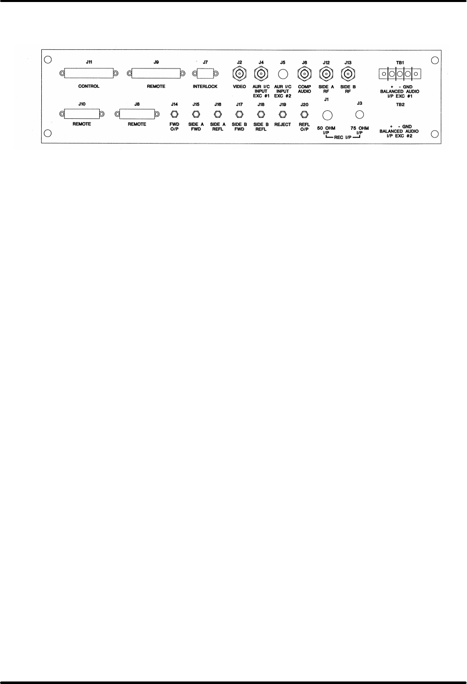
2.1.13 Customer Remote Interface
Connections
The remote monitoring and operation of
the transmitter is provided through the
jacks (J8, J9, and J10) on (A9) the
remote interface assembly mounted on
the rear of the single UHF exciter
assembly (see Figure 2-1).
Digital UHF Transmitter Chapter 2, System Description and
Customer Remote Connections
DT835A, Rev. 1 2-9
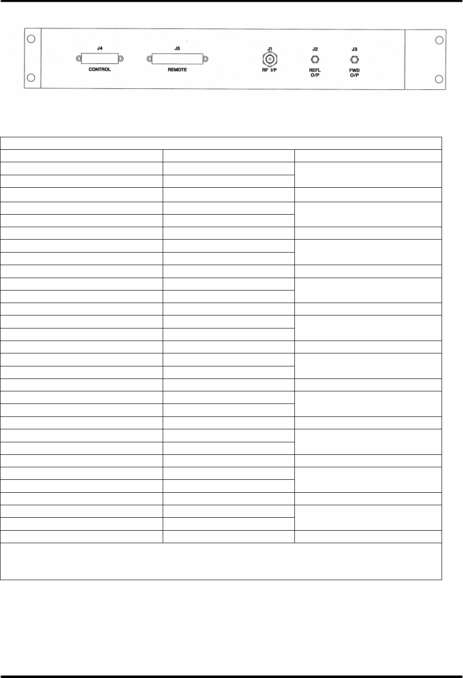
Figure 2-1: Exciter Remote Interface Assembly
Jack (J7) should have a dummy plug
connected to it, with a jumper
connected between pins 1 and 2, to
provide the interlock to the exciter
needed to operate the transmitter. If the
jumper is missing, the transmitter will
not switch to Operate. If remote
connections are made to the
transmitter, they should be made
through the plugs provided in the
installation material for the transmitter
and wired as indicated on the
interconnect drawing for the single UHF
exciter assembly (11056919). The
remote control interface connections for
this transmitter are shown in
Table 2-14.

Digital UHF Transmitter Chapter 2, System Description and
Customer Remote Connections
DT835A, Rev. 1 2-10
Table 2-14: Remote Control Interface Connections
FUNCTION REMOTE JACK/PIN
NUMBER INTERFACE TYPE
Exciter Enable Interlock J7-1
Exciter Enable Interlock Rtn J7-2 J7-1 and 2 must be
jumpered together for
normal operation.
Transmitter Remote Metering
Combined Output Power J10-7
Combined Output Power Rtn J10-8 1V full scale at 1kΩ source
resistance
Combined Reflected Power J10-9
Combined Reflected Power
Rtn J10-10 1V full scale at 1kΩ source
resistance
Exciter Output J9-26
Exciter Output Rtn J9-27 1V full scale at 1kΩ source
resistance
Exciter Remote Control Commands
Exciter Operate (Enable) J8-3 Contact closure
Exciter Standby/Operate Rtn J8-2
Exciter Standby (Disable) J8-1 Contact closure
Exciter Auto J8-6 Contact closure
Exciter Auto/Manual Rtn J8-5
Exciter Manual J8-4 Contact closure
Power Raise (optional) J9-6 Contact closure
Raise/Lower Rtn (optional) J9-5
Power Lower (optional) J9-4 Contact closure
Exc Modulator Select
(optional) J8-10 Contact closure
Exc Modulator Select Rtn
(optional) J8-11
Exciter Remote Status Indications
Exciter Auto Mode Indicator J9-30 50 mA max current sink
Auto/Manual Mode Ind Rtn J9-31
Exciter Manual Mode
Indicator J9-32 50 mA max current sink
Operate Indicator J9-1 50 mA max current sink
Operate/Standby Ind Rtn J9-2
Standby Indicator J9-3 50 mA max current sink

Digital UHF Transmitter Chapter 2, System Description and
Customer Remote Connections
DT835A, Rev. 1 2-11
FUNCTION REMOTE JACK/PIN
NUMBER INTERFACE TYPE
Exciter VSWR Cutback
Indicator J8-7 50 mA max current sink
Video Loss Indicator J9-7 50 mA max current sink
Video Loss Indicator Rtn J9-8
Exc Receiver Fault Ind
(optional) J8-9 50 mA max current sink
Side A Driver Remote Metering
Side A Driver Output Power J10-1
Side A Driver Output Power
Rtn J10-2 1V full scale at 1kΩ source
resistance
Side B Driver Remote Metering
Side B Driver Output Power J10-3
Side B Driver Output Power
Rtn J10-4 1V full scale at 1kΩ
source resistance
Side A Remote Metering
Side A Forward Power J10-14
Side A Forward Power Rtn J10-15 1V full scale at 1kΩ source
resistance
Side A Reflected Power J10-16
Side A Reflected Power Rtn J10-17 1V full scale at 1kΩ source
resistance
Side B Remote Metering
Side B Forward Power J10-20
Side B Forward Power Rtn J10-21 1V full scale at 1kΩ
source resistance
Side B Reflected Power J10-18
Side B Reflected Power Rtn J10-19 1V full scale at 1kΩ source
resistance
Side A + B Remote Metering
Reject Power J10-11
Reject Power Rtn J10-12 1V full scale at 1kΩ source
resistance
The above connections are made to jack (J9), the 37-position “D” connector; to jack
(J10), the 25-position “D” connector; to jack (J8), the 25-position “D” connector; or
to jack (J7), the 9-position “D” connector on (A9) the remote interface assembly
mounted at the top, rear of the single UHF exciter cabinet.
Digital UHF Transmitter Chapter 2, System Description and
Customer Remote Connections
DT835A, Rev. 1 2-12
Figure 2-2: Amplifier Array Remote Interface Panel
Amplifier Array Assembly Remote Metering
(A1) UHF Amp Tray Refl Pwr J5-2
(A1) Reflected Power Rtn J5-1 1V full scale at 1kΩ source
resistance
(A1) UHF Amp Tray Fwrd Pwr J5-4
(A1) Forward Power Rtn J5-3 1V full scale at 1kΩ source
resistance
(A2) UHF Amp Tray Refl Pwr J5-6
(A2) Reflected Power Rtn J5-5 1V full scale at 1kΩ source
resistance
(A2) UHF Amp Tray Fwrd Pwr J5-8
(A2) Forward Power Rtn J5-7 1V full scale at 1kΩ source
resistance
(A3) UHF Amp Tray Refl Pwr J5-9
(A3) Reflected Power Rtn J5-10 1V full scale at 1kΩ source
resistance
(A3) UHF Amp Tray Fwrd Pwr J5-11
(A3) Forward Power Rtn J5-12 1V full scale at 1kΩ source
resistance
(A4) UHF Amp Tray Fwrd Pwr J5-13
(A4) Forward Power Rtn J5-14 1V full scale at 1kΩ source
resistance
(A4) UHF Amp Tray Refl Pwr J5-15
(A4) Reflected Power Rtn J5-16 1V full scale at 1kΩ source
resistance
(A5) UHF Amp Tray Fwrd Pwr J5-18
(A5) Forward Power Rtn J5-17 1V full scale at 1kΩ source
resistance
(A5) UHF Amp Tray Refl Pwr J5-21
(A5) Reflected Power Rtn J5-20 1V full scale at 1kΩ source
resistance
The above connections are made to jack (J5), the 37-position “D” connector on
(A11) the remote interface panel (Figure 2-2) mounted at the top, rear of each of
the amplifier array cabinets.

Digital UHF Transmitter Chapter 3, Installation and Setup Procedures
DT835A, Rev. 0 3-1
Chapter 3
Installation and Setup Procedures
There are special considerations that
need to be taken into account before the
DT835A can be installed. For example, if
the installation is completed during cool
weather, a heat-related problem may not
surface for many months, suddenly
appearing during the heat of summer.
This section provides planning
information for the installation and set up
of the transmitter.
3.1 Site Considerations
The transmitter requires an AC input line
of 220 VAC with a rating of 20 amps for
the exciter cabinet and 100 amps for
each amplifier cabinet. Make sure that
the proposed site for the transmitter has
the voltage requirements that are
needed.
The DT835A is designed and built to
provide long life with a minimum of
maintenance. The environment in which
it is placed is important and certain
precautions must be taken. The three
greatest dangers to the transmitter are
heat, dirt, and moisture. Heat is usually
the greatest problem, followed by dirt,
and then moisture. Over-temperature
can cause heat-related problems such as
thermal runaway and component failure.
Each amplifier tray in the transmitter
contains a thermal interlock protection
circuit that will shut down that tray until
the temperature drops to an acceptable
level.
A suitable environment for the
transmitter can enhance the overall
performance and reliability of the
transmitter and maximize revenues by
minimizing down time. A properly
designed facility will have an adequate
supply of cool, clean air, free of airborne
particulates of any kind, and no
excessive humidity. An ideal environment
will require temperature in the range of
40° F to 70° F throughout the year,
reasonably low humidity, and a dust-free
room. It should be noted that this is
rarely if ever attainable in the real world.
However, the closer the environment is
to this design, the greater the operating
capacity of the transmitter.
The fans and blowers designed and built
into the transmitter will remove the heat
from within the trays, but additional
means are required for removing this
heat from the building. To achieve this, a
few considerations should be taken into
account. The first step is to determine
the amount of heat to be removed. There
are generally three sources of heat that
must be considered. The first and most
obvious is the heat from the transmitter
itself. This can be determined by
subtracting the average power to the
antenna (1500 watts) from the AC input
power (15,000 watts). This number in
watts (13,500) is then multiplied by
3.41, which gives 46,035, the BTUs to be
removed every hour. 12,000 BTUs per
hour equals one ton, so a 4-ton air
conditioner will cool a 1.5 kW digital
transmitter.
The second source of heat is other
equipment in the same room. This
number is calculated in the same way as
the equation for BTUs. The third source
of heat is equally obvious but not as
simple to calculate. This is the heat
coming through the walls, roof, and
windows on a hot summer day. Unless
the underside is exposed, the floor is
usually not a problem. Determining this
number is usually best left up to a
qualified HVAC technician. There are far
too many variables to even estimate this
number without detailed drawings of the
site showing all construction details. The
sum of these three sources is the total
amount of heat that must be removed.
There may be other sources of heat, such
as personnel, and all should be taken into
account.

Digital UHF Transmitter Chapter 3, Installation and Setup Procedures
DT835A, Rev. 0 3-2
Now that the amount of heat that must
be removed is known, the next step is to
determine how to accomplish this. The
options are air conditioning, ventilation,
or a combination of the two. Air
conditioning is always the preferred
method and is the only way to create
anything close to an ideal environment.
Ventilation will work quite well if the
ambient air temperature is below 100° F,
or about 38° C, and the humidity is be
kept at a reasonable level. In addition,
the air stream must be adequately
filtered to ensure that no airborne
particulate of any kind will be carried into
the transmitter. The combination of air
conditioning for summer and ventilation
during the cooler months is acceptable
when the proper cooling cannot be
obtained through the use of ventilation
alone and using air conditioning
throughout the year is not feasible.
Caution: The operation of air
conditioning and ventilation
simultaneously is not recommended.
This can cause condensation in
transmitters. For tube type
transmitters, this can be especially
serious if the condensation forms in
the tube cavity and creates
damaging arcs.
The following precautions should be
observed regarding air conditioning
systems:
1. Air conditioners have an ARI
nominal cooling capacity rating. In
selecting an air conditioner, do not
assume that this number can be
equated to the requirements of
the site. Make certain that the
contractor uses the actual
conditions that are to be
maintained at the site in
determining the size of the air
conditioning unit. With the desired
conditioned room temperature
under 80° F, the unit must be
derated, possibly by a substantial
amount.
2. Do not have the air conditioner
blowing directly onto the
transmitter. Condensation may
occur on, or worse in, the
transmitter under certain
conditions.
3. Do not isolate the front of the
transmitter from the back with the
thought of air conditioning only
the front of the unit. Cooling air is
drawn in at the front of all
transmitters and in the front and
back of others. Any attempt to
isolate the front from the rear will
adversely affect the cooling air
flow.
4. Interlocking the transmitter with
the air conditioner is
recommended to keep the
transmitter from operating without
the necessary cooling.
5. The periodic cleaning of all filters
is a must.
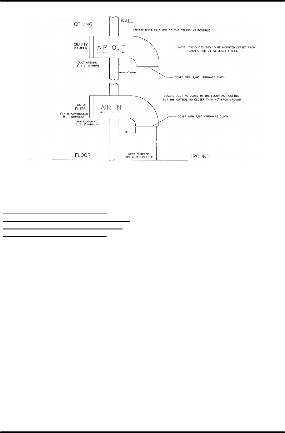
When using ventilation alone, the
following general statements apply:
1. The blower, with attendant filters,
should be on the inlet, thereby
pressurizing the room and
preventing dirt from entering the
transmitter.
2. The inlet and outlet vents should
be on the same side of the
building, preferably the leeward
side. As a result, the pressure
differential created by wind will be
minimized. Only the outlet vent
may be released through the roof.
3. The inlet and outlet vents should
be screened with 1/8" hardware
cloth (preferred) or galvanized
hardware cloth (acceptable).
4. Cooling air should enter the room
as low as practical but in no case
higher than four feet above the
floor. The inlet must be located

Digital UHF Transmitter Chapter 3, Installation and Setup Procedures
DT835A, Rev. 0 3-3
where dirt, leaves or snow will not
be carried in with the cooling air.
5. The exhaust should be located as
high as possible. Some ducting is
usually required to insure the
complete flushing of heated air
with no stagnant areas.
6. The filter area must be adequate
to insure a maximum air velocity
of 300 feet per minute through the
filter. This is not a conservative
number but a never-exceed
number. In a dusty or remote
location, this number should be
reduced to 150 CFM.
7. The inlet and outlet(s) must have
automatic dampers that close any
time the ventilation blower is off.
8. In those cases in which
transmitters are regularly off for a
portion of each day, a
temperature-differential sensor
that controls a small heater must
be installed. This sensor will
monitor inside and outside
temperatures simultaneously. If
the inside temperature falls to
within 5° F of the outside
temperature, the heater will come
on. This will prevent condensation
when the ventilation blower comes
on and applies even in the
summer.
9. A controlled-air bypass system
must be installed to prevent the
temperature in the room from
falling below 40° F during
transmitter operation.
10. The blower should have two
speeds, which are thermostatically
controlled, and interlocked with
the transmitter.
11. The blower on high speed must be
capable of moving the required
volume of air into a half inch of
water pressure at the required
elevation. The free air delivery
method must not be used.
12. Regular maintenance of any filters
can not be overemphasized.
13. Tube transmitters should not rely
on the internal blower to exhaust
cooling air at elevations above
4000 feet. For external venting,
the air vent on the cabinet top
must be increased to an 8"
diameter for a 1 kW transmitter
and to 10" for 5 kW and 10 kW
transmitters. An equivalent
rectangular duct may be used but,
in all cases, the outlet must be
increased in area by 50% through
the outlet screen.
14. It is recommended that a site plan
be submitted to Axcera for
comments before installation
commences.
In calculating the blower requirements,
filter size, and exhaust size, if the total
load is known in watts, 2000 CFM into
1/2" of water will be required for each
5000 watts. If the load is known in BTUs,
2000 CFM into 1/2" of water will be
required for each 17,000 BTUs. The inlet
filter must be a minimum of seven
square feet, larger for dusty and remote
locations, for each 5000 watts or 17,000
BTUs. The exhaust must be at least four
square feet at the exhaust screen for
each 5000 watts or 17,000 BTUs.
The information presented in this section
is intended to serve only as a general
guide and may need to be modified for
unusually severe conditions. A
combination of air conditioning and
ventilation should not be difficult to
design (see Figure 3-1). System
interlocking and thermostat settings
should be reviewed with Axcera. As with
any equipment installation, it is always
good practice to consult the
manufacturer when questions arise.
Axcera can be contacted at
(724) 873-8100.
Digital UHF Transmitter Chapter 3, Installation and Setup Procedures
DT835A, Rev. 0 3-4
Figure 3-1. 1 kW Minimum Ventilation Configuration
3.2 Unpacking the Cabinets and
Trays
Note: Air conditioning and any
related heat exhaust ducts should be
in place before continuing with the
installation of the transmitter.
Thoroughly inspect the cabinets and all
other materials upon their arrival. Axcera
certifies that upon leaving our facility the
equipment was undamaged and in proper
working order. The shipping containers
should be inspected for obvious damage
that indicates rough handling. Check for
dents and scratches or broken switches,
meters, or connectors. Any claims
against in-transit damage should be
directed to the carrier. Inform Axcera as
to the extent of any damage as soon as
possible.
Remove the cabinets, trays, hybrid
combiner, bandpass filter, trap filter, and
output couplers, along with any
installation material, from the crates and
boxes. Remove the straps that hold the
cabinets to the shipping skids and slide
the cabinets from the skids. Remove the
plastic wrap and foam protection from
around the cabinets. Do not remove any
labeling or tags from any cables or
connectors. These are identification
markers that make reassembly of the
transmitter much easier.
3.3 Installing the Cabinets and Trays
There are three cabinets: (A1) the single
UHF exciter assembly, (A2) the side A
amplifier array assembly, and (A3) the
side B amplifier array assembly. With the
operator facing the cabinets, they should
be arranged from left to right with the
single UHF exciter cabinet on the left, the
side A amplifier cabinet in the center, and
the side B amplifier cabinet on the right.
The cabinets should be positioned with
consideration given to adequate air
intake and exhaust, the opening of the
rear door, access to the trays (including
sliding them out for testing), the AC
hookup, and the installation of the output
transmission line. The cabinets should be
grounded using copper strapping
material and should also be permanently
mounted to the floor of the site using the
holes in the bottom of the cabinets.

Digital UHF Transmitter Chapter 3, Installation and Setup Procedures
DT835A, Rev. 1 3-5
If trays are pre-mounted in the exciter
cabinet, remove the two L-brackets,
mounted on the front panel rails of the
single exciter cabinet, which hold the
trays in place during shipment. The UHF
amplifier trays are shipped separately
from the amplifier array cabinets because
of the weight of each tray. The trays are
mounted in the cabinet using Chassis
Trak cabinet slides. The tray slides are on
the top and bottom of the UHF amplifier
trays and on the sides of the UHF exciter
tray and the variable phase/gain trays.
Inspect the trays for any loose hardware
or connectors, tightening where needed.
Open the rear door; the key to unlock
the door, if the door has the optional
lock, is found in a tan envelope taped to
the door. Inspect the interior for packing
material and carefully remove any
packing material that is found. Slowly
slide each tray in and out to verify that
they do not rub against each other and
have no restrictions to free movement.
Note: The UHF amplifier trays must
be placed into the cabinets in the
proper location, and according to the
labeling on each tray, or the gain and
the phasing will not be maximized.
The UHF amplifier trays are labeled to
indicate where they are positioned in the
side A or the side B amplifier cabinets.
They are mounted in each cabinet from
bottom left to top right, with A1 the
bottom, left tray and A6 (if used) the top,
right tray. Locate the tray labeled A1 and
slide it into the side A cabinet in the
bottom, left position. Locate the tray
labeled A2 and slide it into the side A
cabinet in the bottom, right position.
Locate the tray labeled A3 and slide it
into the side A cabinet in the middle, left
position. Locate the tray labeled A4 and
slide it into the side A cabinet in the
middle, right position. Locate the tray
labeled A5 and slide it into the side A
cabinet in the top, left position.
Locate the UHF amplifier tray labeled B1
and slide it into the side B cabinet in the
bottom, left position. Locate the tray
labeled B2 and slide it into the side B
cabinet in the bottom, right position.
Locate the tray labeled B3 and slide it
into the side B cabinet in the middle, left
position. Locate the tray labeled B4 and
slide it into the side B cabinet in the
middle, right position. Locate the tray
labeled B5 and slide it into the side B
cabinet in the top, left position. All of the
amplifier trays should now be installed.
Slowly slide each tray in and out to verify
that they do not rub against each other
and have no restrictions to free
movement.
Caution: Each UHF amplifier tray has
a hard-line coaxial cable connected
to the rear panel. The tray will not
slide out without first removing this
connection.
In order to pull out the tray for test
purposes or other reasons, use the test
cable included in the installation material
kit for connections from the tray to the
output cable.
It may be necessary to make
adjustments to the positions of the trays.
This can be accomplished by loosening
the cabinet slide mounting bolts that hold
the front of the slide to the mounting
frame of the cabinet and moving the tray
up or down or left or right, as needed, to
correct for any misalignment.
3.3.1 DM8-R Modulator Installation
1. If not pre-mounted, remove the
modulator tray from the shipping box
and inspect it for any damage that
may have occurred during shipment.
Remove all packing material used to
protect the unit during shipment.
2. The tray mounts using four clearance
holes into a standard 19" rack or
cabinet. Mount the tray into the
cabinet and adjust or align the tray
so that it does not interfere with
cabling or other trays.

Digital UHF Transmitter Chapter 3, Installation and Setup Procedures
DT835A, Rev. 1 3-6
3. Verify that the circuit breaker (CB1),
located on the rear of the tray, and
the main circuit breaker for the
system are off.
4. Connect the AC power cord, provided
in the installation kit, to J1, the AC
input jack on the rear of the tray.
5. Connect the MPEG input to J2, the IF
output from J4, and the 10 MHz
reference input, if supplied, to J3 on
the rear of the tray.
6. Connect the IF output at J4 to the
digital IF input to the upconverter of
the system.
This completes the installation procedure
for the DM8-R modulator.
3.4 Main AC Inputs
Once the cabinets are in place, and the
trays have been checked for damage and
alignment, the main AC hookup is ready
to be made.
Caution: Before connecting the
208/240 VAC, make certain that all
of the circuit breakers associated
with the transmitter are switched
off.
There are three AC input circuits to the
DT835A transmitter: one is 20 amps and
the two others are 100 amps single
phase. The input AC to the exciter
cabinet should be a 20 amp, 208/240
VAC line. The input AC to each amplifier
cabinet should be a single-phase, 100
amp, 208/240 VAC line.
The 20-amp, 208/240 VAC input
connections are made to the terminal
block A1-TB1, part of the AC distribution
assembly, exciter cabinet (1245-1500),
near the center, right-hand side, rear
portion of cabinet #1. Connect terminal 1
to line 1, terminal 3 to line 2 (208/240
VAC), and terminal 2 to the chassis
ground.
For single phase - Connect one of the
100-amp, 208/240 VAC inputs to the
terminal block A3-TB1, part of the AC
distribution assembly, amplifier
assembly (1278-1100), near the center,
right-hand side, rear portion of cabinet
#2. Connect line 1 to TB1-1A, line 2 to
TB1-3A and the safety ground to TB1-
4A. Follow the same procedure for
cabinet #3.
3.5 Output Connections
The RF output of the (A2) amplifier
assembly connects through (A5) a 1-5/8"
to 3-1/8" adapter to J1 on (A4) the
hybrid combiner. The RF output of the
(A3) amplifier assembly connects
through (A6) a 1-5/8" to 3-1/8" adapter
to J2 on (A4) the hybrid combiner. The
reject output of the combiner at J4
connects through (A12) a 1-5/8” to 3-
1/8” adapter to (A7) a directional coupler
(1016-1043) and then to (A8) the 2500-
watt reject load. The combined RF output
of the combiner at J3 connects through
(A9) the bandpass filter to (A10) the
output trap filter assembly. The filtered
output connects through (A11) the
output coupler assembly (1020-1002) to
the transmission line that is connected to
the antenna.
This completes the unpacking and
installation procedures for the DT835A
transmitter. Refer to the setup and
operation procedures that follow before
applying power to the transmitter.

Digital UHF Transmitter Chapter 3, Installation and Setup Procedures
DT835A, Rev. 1 3-7
Table 3-2: Jumper Positions in the Gain 1 and Gain 2 Circuits for an
Input Level of Between –6 and –26 dBm
IF Input Range W3 on J4 and W4 on J5 W5 on J6 and W6 on J7
-11 to -6 dBm Low Low
-16 to -11 dBm Low High
-21 to -16 dBm High Low
-26 to -21 dBm High High
3.6 Setup and Operation Procedures
The transmitter should initially be turned
on with the RF output at J2 of the (A11)
output coupler assembly terminated into
a dummy load. If a load is not available,
check that the output of the coupler
assembly at J2 is connected to the
antenna. Connect the digital IF input to
J6 on the rear of the UHF exciter tray. On
(A5) the 5 Section delay equalizer board,
44 MHz, set the input matching jumpers
J2 and J3 to positions 1 and 2 for a 50Ω
input, or to positions 2 and 3 for a 75Ω
input, as needed. Depending on the input
level, two gain circuits on the delay
equalizer board, 44 MHz, are adjusted
using jumpers, W3-W6, to set the gain
through the board. Table 3-2 shows the
jumper positions in the gain 1 and gain 2
circuits for an input level of between -6
to -26 dBm.
Switch on the main AC circuit breaker on
the AC distribution assembly mounted
toward the rear of the single UHF exciter
assembly. Switch on the main AC circuit
breakers on the AC distribution
assemblies mounted toward the rear of
the amplifier cabinets. Switch on the
CB2-CB6 circuit breakers for the
individual UHF amplifier trays on the AC
distribution assemblies mounted in each
amplifier array cabinet.
Switch the Operate/Standby switch on
the UHF exciter to standby and the
Auto/Manual switch, also on the UHF
exciter, to Auto. Normal operation of the
transmitter is with the switch in
Automatic. Automatic operation of the
exciter uses the digital input to the
exciter as an Operate/Standby switch. In
Auto, if the input is lost, the exciter will
automatically cause the transmitter to
revert to Standby. When the input signal
is restored, the exciter will automatically
return the transmitter to Operate.
Move the Operate/Standby switch on the
exciter to Operate. Observe the power
supply readings on the front panel
meters of the UHF amplifier trays in each
amplifier cabinet assembly; the reading
should be +26.5 VDC.
Note: If the transmitter does not
switch to Operate when the
Operate/Standby switch is switched
to Operate, check that there is an
external interlock plug connected to
jack (J7) on the remote interface
assembly mounted in the top, rear of
the single UHF exciter cabinet. Make
sure that the plug has a jumper from
pins 1 to 2 to provide the interlock
for the exciter. The interlock must be
present for the transmitter to
operate.
Observe the front panel meter on the
metering panel with the switch in the
Combined Visual Output Power position;
it should read 100%. If needed, adjust
the power adjust screwdriver pot on the
front panel of the UHF exciter to attain a
100% reading on the front panel meter.
At the same time that the output power
is being observed, check the meter
readings on the metering panel and the
combined meter, in the % Reflected
Power position, for the side A and side B
amplifier assemblies. If the % Reflected
Power for any of the readings is very
high, above 50%, a problem is present
with the output coaxial lines in the side A
amplifier assembly or in the output lines

Digital UHF Transmitter Chapter 3, Installation and Setup Procedures
DT835A, Rev. 1 3-8
for the system and needs to be checked
and corrected. A center bullet missing
from the 1-5/8" or 3-1/8" rigid coax lines
or loose bolts on the connections can
cause this problem. Return the
Operate/Standby switch to Standby.
Observe the % Exciter Power reading of
the meter on the exciter; it should be the
same as on the Test Data Sheet for the
transmitter, typically 70%. Move the
Operate/Standby switch on the exciter to
Standby.
The gain and phase controls on the front
panels of the individual UHF amplifier
trays were adjusted at the factory to
attain 100% output of the transmitter
and should not need to be readjusted.
The forward meter readings for side A
and side B may not be the same, but
should be the same as the values written
on the Test Data Sheet. Side A and side
B are combined to give the total output,
which is 100% in the combined output
power position.
The readings on each of the individual
UHF amplifier trays may not be the
same. Refer to the Test Data Sheet and
compare the final readings from the
factory with the readings on each of the
trays after the setup. They should be
very similar. If a reading is way off, refer
to the phasing and power adjustment
procedures for the UHF amplifier trays in
Chapter 5, Detailed Alignment
Procedures, of this manual before trying
to make any adjustments.
If a dummy load is connected to the
transmitter, switch the transmitter to
Standby and switch off the main AC
circuit breakers found on the AC
distribution panels in each cabinet.
Remove the dummy load and make all of
the connections needed to connect the
transmitter to the antenna. Switch the
main AC circuit breakers on and the
Operate/Standby switch to Operate.
Adjust the exciter power adjust pot to
attain 100% combined visual output.
If the transmitter is already connected to
the antenna, check that the combined
power output is 100%. If necessary,
adjust the power adjust pot located on
the UHF exciter for 100%.
3.6.1 DM8-R Modulator Setup
Procedures
NOTE: The modulator was setup at the
factory to meet specifications for digital
mask and corrections and should not
need adjusted.

Digital UHF Transmitter Chapter 4, Circuit Descriptions
DT835A, Rev. 1 4-1
Chapter 4
Circuit Descriptions
4.1 (A1) UHF Exciter Assembly
The (A1) UHF Exciter Assembly
contains (A1) a UHF Exciter Tray
(1142445), (A4 & A5) two Variable
Gain/Phase Trays (1245-1200), (A6) a
Metering Panel (1061456), (A8) an AC
Distribution Assembly, Exciter (1245-
1500) and (A9) a Remote Interface
Assembly (1061198).
The (A1) UHF Exciter Tray (1142445),
takes the Digital IF Input that is
upconverted to the On Channel RF by
mixing it with a L.O. signal generated
by the Channel Oscillator Assembly.
The RF Output of the UHF Exciter at J15
connects to (A3) a Splitter which splits
the RF two ways with the RF Output #1
connected to the input of the (A5)
Variable Gain/Phase Tray (1245-1200)
and the RF Output #2 connected to the
input of the (A4) Variable Gain/Phase
Tray (1245-1200). The output of the
(A4) Variable Gain/Phase Tray connects
to (A2) the Side A Amplifier Assembly
(1278-1300). The output of the (A5)
Variable Gain/Phase Tray connects to
(A3) the Side B Amplifier Assembly
(1278-1300).
4.1.1 Control and Status
The Control and Status of the
Transmitter are provided by the Meter
indications on the Metering Panel and
the Variable Gain Phase Trays. There
are also Control, Status and LED
Indications located on the front panel of
the UHF Exciter Tray. The switches and
LED indicators, which are mounted so
that the switches and LEDs are
operated or viewed from the front
Panel of the UHF Exciter, are part of the
Transmitter Control Board (1245-
1101). On the UHF Exciter Tray, switch
(S1) is an Operate/Standby Switch that
provides the Operate Commands
(Enables), when in Operate, to each of
the Amplifier Arrays. The Enable is
needed to turn on the Switching Power
Supplies located in each of the UHF
Amplifier Trays. When the UHF Exciter
is in Operate, the Green LED (DS2) is
On and when in Standby the Amber
LED (DS1) is On. NOTE: If the
Transmitter does not switch to Operate,
when S1 is switched to Operate, check
that a Dummy Jumper Plug is
connected to Jack J7, with a Jumper
between Pins 1 & 2, located on (A9) the
Remote Interface Assembly in the
Single UHF Exciter Assembly. The
Jumper provides the Interlock to the
UHF Exciter needed for the operation of
the Transmitter. If the Interlock is
present, the Green LED (DS5), located
on the Transmitter Control Board,
should be lit.
Operation of the Transmitter is
controlled by the front panel switches
located on the UHF Exciter Tray.
During Normal operation of the
Transmitter, Switch S2 should be in the
Auto position. The front panel of the
UHF Exciter also has LEDs that indicate
a Input Fault (Loss), Red LED (DS9)
and a VSWR Cutback, Amber LED
(DS7).
4.1.2 Digital Input and Remote
Connections
The Digital Input to the Transmitter,
connects to the (A9) Remote Interface
Panel located on the rear of the Single
UHF Exciter Assembly. The Digital
Input connects to Jack J2 that is cabled
to J2 on the DM8-R Modulator.
Remote Monitoring and Operation of
the Transmitter is provided through the
Jacks (J8, J9 & J10) located on (A9) the
Remote Interface Assembly mounted
toward the rear of the Single UHF
Exciter Assembly. Jack (J7) should
have a dummy plug connected to it,

Digital UHF Transmitter Chapter 4, Circuit Descriptions
DT835A, Rev. 1 4-2
which has a jumper connected between
Pins 1 & 2, that provides the Interlock
to the Exciter needed to operate the
Transmitter. If the Jumper is missing,
the Transmitter will not switch to
Operate. If remote connections are
made to the Transmitter, they should
be made through the plugs provided in
the Installation Material as noted on the
Interconnect Drawing (1056919 or
1278-8400) for the Single UHF Exciter.
4.1.3 AC Input
The Single UHF Exciter Assembly needs
an AC input of 208/240 VAC at 20
Amps. The AC Input to the Single UHF
Exciter Assembly connects to (A8) the
AC Distribution Assembly, UHF Exciter
Assembly (1245-1500) located in the
right, center rear of the Cabinet. The
Assembly contains the 4 Terminal Block
(TB1) to which the 208/240 VAC
connects. Line 1 to TB1-1, Line 2 to
TB1-3 and Safety Ground to TB1-2.
The AC Distribution Panel contains one
Circuit Breaker that supplies the AC to
the rest of the Single Exciter Assembly.
The Input AC is connected to (CB1) the
Main AC Circuit Breaker (20 Amps).
The output of CB1 has three MOVs,
VR1, VR2 and VR3, connected to it, one
connected from each leg of the Input
AC to ground and one across the two
legs. The AC output of CB1 connects to
A1 and A2 which are IEC Outlet Strips.
The (A1) Exciter 1 and the (A4)
Variable Gain/Phase Tray plug into the
(A1) IEC Outlet Strip. The (A5)
Variable Gain/Phase Tray, the (A8)
Metering Panel and the 8 VSB
Modualtor Tray plug into the (A2) IEC
Outlet Strip.
When the Circuit Breaker CB1,
mounted on the AC Distribution
Assembly, is switched On, +12 VDC
from the Exciter, is supplied to each of
the Amplifier Array Cabinets for the
operation of the LED Status Indicators
in each of the UHF Amplifier Trays.
4.2 (A19) DM8-R Digital Modulator
(1306978; Appendix C)
4.2.1 (A1) DM8 Modulator Board
(1304883; Appendix D)
4.2.1.1 SMPTE-310 Input
The DM8-R modulator accepts a
SMPTE-310 input the BNC Jack J2
located on the rear panel of the tray.
This input is connected to J42 on the
Digital Modulator Board via a RG-179
cable. This input is applied to a high
speed window comparator that adjusts
the level to a low voltage TTL signal to
be used by the Altera FPGA, U3. The
SMPTE-310 signal is input to the FPGA
to recover the clock and the data. A
portion of the clock and recovery
circuit is performed by a high speed
comparator, U17, that functions as an
external delay circuit.
4.2.1.2 Channel Coder
The FPGA subsequently uses the
SMPTE-310 clock and data as the input
to the channel coder contained inside
the FPGA. The channel coder is a
series of DSP blocks defined by the
ATSC standard for 8 VSB data
transmission. These blocks include the
data randomizer, Reed Solomon
Encoder, data interleaver, trellis coder,
and sync insertion. The channel
coder portion inside the FPGA
generates the 8 distinct levels in an 8
VSB transmitter. These levels are
subsequently input to a linear
equalizer that provides for frequency
response correction in the
transmission path. The linear
equalizer is a 67 tap FIR filter that is
loaded with tap values from the
microntroller, U1, located on this
board. The output of the linear
equalizer is then input to two pulse
shaping filters, an in phase (I) and a
quadrature (Q) filter that are also
located inside the FPGA. The pulse
shaping filters are FIR filters that have
fixed tap values that are preset inside

Digital UHF Transmitter Chapter 4, Circuit Descriptions
DT835A, Rev. 1 4-3
the FPGA. The output of the pulse
shaping filters is then applied to a Pre-
Distortion Linearizer chip, U4, which
can be used to correct for
nonlinearities in the data transmission
path. The output of the Pre-Distortion
chip is gain scaled and output to a dual
D/A converter that output a baseband
I and Q analog signal.
4.2.1.3 Analog Output Section
The baseband I and Q signals from the
D/A converter are applied to
differential analog filters that remove
some of digital artifacts from the D/A
conversion process. The output of the
I channel filter is then mixed with the
pilot frequency, 46.69 MHz, using
mixer U30. The output of the Q filter
is mixed with the pilot frequency that
is phase shifted 90 degrees using
mixer U34. The mixers are current
driven devices so that when the
outputs of U30 and U34 are connected
together, they provide a combined
output. This combined output is
subsequently input to a final
differential output filter which provides
the final IF output at the SMA
connector, J38. This output is
connected through a RG-174 cable to
the BNC connector J4, the IF output
jack, located on the rear panel of the
tray.
4.2.1.4 Pilot Frequency Generation
The 46.69 MHz pilot signal, which is
used in the mixing process, is
generated from a 46.69 MHz VCXO
that is phase locked to a 10 MHz
reference. The VCXO and the 10 MHz
are divided down to a common
frequency, which is then compared
internal to the FPGA. The FPGA
subsequently provides error signals to
a analog phase locked implemented
with op amp stages U45-A, B and C.
The output of these compensation
stages is used as the control voltage to
the VCXO, U37. The phase locked
output of U37 is applied to a analog
filter to remove harmonics of the pilot
and then input to quadrature splitter
Z1. The outputs of Z1 are used as the
inputs to the mixers in the analog
output section.
4.2.2 (A2) DM8-R Front Panel
Board (1307113; Appendix D)
The front panel board contains four
LEDs, Power, MPEG, PLL A and PLL B,
which are viewable on the front panel.
J2 connects to the Modulator Board,
which controls the operation of the
LEDs. When the system is operation
normally, all LEDs will be Green. If a
problem occurs, that LED will not be
lit.
4.3 (A4) UHF Exciter Tray (1142445
or 1294-1111; Appendix C)
4.3.1 (A12 and A18) UHF Filter
(1007-1101; Appendix D)
The UHF filter is a tunable two-section
cavity filter that is typically tuned for a
bandwidth of 5 MHz and has a loss of -
1 dB through the filter.
4.3.2 (A15-A1) UHF Generator
Board (1565-1109; Appendix D)
The UHF generator board is mounted in
the UHF Generator Enclosure (1519-
1144) for EMI and RFI protection. The
board contains a VCXO circuit and
additional circuitry to multiply the VCXO
frequency by eight. The VCXO produces
an output of ≈ 67 MHz to 132 MHz,
depending on the desired channel
frequency. Course adjustment to the
frequency is made by C11, while fine
adjustments are accomplished by the
AFC voltage from (A11) the PLL board
(1286-1104). The VCXO frequency level
is adjusted by C6, L2, and L4. The
output is split and provides an input to
the x8 multiplier circuitry as well as a
sample for the PLL board.

Digital UHF Transmitter Chapter 4, Circuit Descriptions
DT835A, Rev. 1 4-4
The x8 circuitry consists of three
identical x2 broadband frequency
doublers. The input signal at the
fundamental frequency is fed through a
6-dB pad consisting of R21, R24, and
R25 to amplifier U3. The output of the
amplifier stage is directed through a
bandpass filter consisting of L8 and
C32, which is tuned to the fundamental
frequency (67 MHz to 132 MHz). The
voltage measured at TP1 is typically +.6
VDC. The first doubler stage consists of
Z1 with bandpass filter L9 and C34
tuned to the second harmonic (134 MHz
to 264 MHz). The harmonic is amplified
by U4 and again bandpass filtered at
the second harmonic by C38 and L11
(134 MHz to 264 MHz). The voltage
measured at TP2 is typically +1.2 VDC.
The next doubler stage consists of Z2
with bandpass filter C40 and L12 tuned
to the fourth harmonic of the
fundamental frequency (268 MHz to
528 MHz). The fourth harmonic is then
amplified by U5 and fed through
another bandpass filter tuned to the
fourth harmonic consisting of L14 and
C44 (268 MHz to 528 MHz). The voltage
measured at TP3 is typically +2.0 VDC.
The final doubler stage consists of Z3
with bandpass filter C46 and L15 tuned
to the eighth harmonic of the
fundamental frequency (536 MHz to
1056 MHz). The signal is amplified by
U6 and U7 to a typical value of from +2
to +4 VDC as measured at TP4. The
amplified eighth harmonic is then fed to
the SMA output jack of the board at J3.
Typical output level of the signal is +16
dBm nominal.
The +12 VDC for the board enters
through jack J4-3 and is filtered by L22
and C54-C58 before being distributed to
the circuits on the board.
4.3.3 (Optional) (A14-A1) 10-MHz
Reference Generator Board (1519-
1126; Appendix D)
The 10-MHz reference generator board
is located in (A10) the (Optional) 10-
MHz reference kit (1286-1108). The
board contains a high-stability crystal
oscillator that provides a 10-MHz
output that is used as reference
frequency for the transmitter. The
board is mounted within an enclosed
assembly that helps to maintain the
operating temperature of the oscillator
board.
The oscillator operates at 10 MHz.
Transistor Q1 is the oscillating
transistor with the frequency of
oscillation set by the crystal Y1. L2, C2,
and C3 have second-order effects on
the frequency, with C2 and C3 used to
pull the oscillator exactly on frequency.
Capacitors C4 and C5 provide the
positive feedback necessary for
oscillation.
The output of the oscillator is buffered
by Q2 and Q3. L4 and C12 form a 40-
MHz bandpass filter. The 40-MHz signal
passes through a digital divider IC U4,
which divides the signal down to 10
MHz. Transistor Q5 provides a buffered,
10-MHz output at jack J1.
The crystal is heated in an enclosed
crystal oven (HR-1) that is internally
set at 60° C. The oscillator board is
heated by a separate oven that is set at
50° C. U1 is a temperature
sensor/controller IC that monitors the
temperature of the oscillator assembly
and controls the operation of Q4 and
U2. The operating temperature of the
assembly is set by adjusting R15. If the
temperature of the assembly falls
below 50° C, U1 will bias Q4 on, which
in turn increases the amount of current
flow through U2.
The flange of U2 is thermally connected
to the heatsink of the assembly. The
temperature of the heatsink will
increase as the current through U2
increases. As a result, U2 will dissipate
more power in the form of heat, and
the temperature of the assembly will
increase. If the assembly temperature
rises above 50° C, the opposite action

Digital UHF Transmitter Chapter 4, Circuit Descriptions
DT835A, Rev. 1 4-5
will occur, thus lowering the
temperature of the assembly.
The +12 VDC enters the board at J2
and is filtered by L1 and C1 before it is
applied to the remaining circuits on the
board.
4.3.4 (A13) PLL Board (1286-1104;
Appendix D)
The PLL board is part of the phase lock
loop (PLL) circuit, which provides the
automatic frequency control (AFC)
voltage, that connects to the VCXO
assembly, and maintains the accurate
output frequency of the VCXO. The AFC
is generated by comparing a sample of
the 10-MHz reference to a sample of
the VCXO frequency. The PLL board
uses an external 10-MHz signal as the
reference unless it is missing, then an
internally generated 10-MHz signal is
used. The two 10-MHz reference
signals are connected to the K1 relay
and the selected reference to U1. The
switching between the two references
is accomplished by the K1 relay which,
when energized, applies the external
10-MHz reference to U1, as long as an
externally generated 10-MHz reference
signal is present and an interlock is
connected to J8, pin 1.
If the interlock is removed or the
external 10-MHz reference is missing,
the relay is de-energized and the
internal 10-MHz reference is applied
through the relay to U1. The internally
generated 10-MHz reference connects
from J7 to pins 3 and 6 of relay K1. The
externally generated 10-MHz reference
connects from J2 to pins 2 and 5 of
relay K1. The unused 10-MHz reference
is connected through the relay to R10,
a 51-Ω load.
With the relay energized, the internally
generated 10-MHz reference from J7
connects through the closed contact of
the relay from pin 6 to pin 7 to R10,
the 51-Ω load. The externally
generated 10-MHz from jack J2
connects through the closed contact of
the relay from pin 2 to pin 1 to
amplifier U1. With the relay not
energized, the internally generated 10-
MHz reference from J7 connects
through the closed contact of the relay
from pin 3 to pin 1 to amplifier U1. The
externally generated 10-MHz from jack
J2 connects through the closed contact
of the relay from pin 5 to pin 7 to R10,
the 51-Ω load.
External 10-MHz Reference Present
Circuitry
The external 10-MHz reference signal
enters the board at J2 and is filtered by
C4, L2, and C5 before it is connected to
the K1 relay. A sample of the 10 MHz is
rectified by CR3 and connected to U3A.
If the sample level of the external 10
MHz is above the reference set by R13
and R14, which is connected to pin 2 of
U3A, the output of U3A stays high. The
high connects to gates of Q4 and Q9,
which are biased on and cause their
drains to go low. The low from the
drain of Q9 is wired to J8, pin 6, for
connection to a remote external 10-
MHz present indicator. The low from
the drain of Q4 connects to the green
LED DS2 which lights to indicate that
an external 10-MHz reference is
present. The low from the drain of Q4
also connects to the gate of Q5, biasing
it off and causing its drain to go high.
This high reverse biases CR4 and allows
a high to be applied to the gates of Q6,
Q8, and Q3, if an interlock, low, is
present at J8, pin 1. The high to the
gate of Q6 biases it on and causing its
drain to go low; the low is connected to
the green LED DS3, which lights,
indicating that an external 10-MHz
reference is selected. The high to the
gate of Q8 biases it on and applies a
low to J8, pin 7, for connection to a
remote reference select indicator. The
high that is applied to the gate of Q3
biases it on and causes its drain to go
low, which energizes the K1 relay and

Digital UHF Transmitter Chapter 4, Circuit Descriptions
DT835A, Rev. 1 4-6
applies the external 10-MHz reference
signal to U1 for use in the PLL circuits.
Internal 10-MHz Reference Circuitry
The internally generated 10-MHz
reference signal connects from jack J7
on the board to pins 3 and 6 of relay
K1. If the external 10-MHz reference is
missing, or the interlock is not present
at J8, pin 1, the relay is de-energized.
The internally generated 10-MHz
reference connects through the closed
contact of the relay from pin 3 to pin 1
to amplifier U1. The externally
generated 10-MHz signal from jack J2
connects through the closed contact of
the relay from pin 5 to pin 7 to R10,
the 51-Ω load.
Sample Input Circuitry
A sample of the signal from the UHF
generator board connects to SMA jack
J9, the sample input on the board. The
signal is amplified by U8 and coupled to
U9, a divide by 20/21 IC. A sample of
the output of U8 is connected to J10,
the sample output jack on the board,
which is typically connected to the front
panel of the tray.
Comparator Phase Lock Loop Circuit
The selected 10-MHz reference
connects to amplifier IC U1 whose
output is split by the circuit consisting
of L3, L4, and R8. A sample of the 10-
MHz reference is cabled to jack J3, the
10-MHz output jack, which is connected
to J5 on the rear of the tray. The 10-
MHz reference connects to IC U4, a
divider PLL chip. The divided-down
sample of the 10-MHz reference, which
is measurable at TP2, connects from
pin 10 of U4 to pin 27 of U5.
The divided-down sample from U9 is
connected to U5, a divider comparator
IC, which divides this signal to a 50-
kHz reference. The 50-kHz references
are compared in the U5 IC to a 50-kHz
sample of the 10-MHz signal that is
generated from an external 10-MHz
reference input or internally from a 10-
MHz reference kit. The three DIP
switches, SW1, SW2, and SW3, are set
up to divide down the reference sample
input generated by the VCXO to 50
kHz. The reference is then compared to
the 50-kHz sample from the 10-MHz
input in the U5 IC.
The output of U5 at pins 7 and 8
connect to U6A, a differential
comparator, whose output is the
difference between the two 50-kHz
references which is the AFC voltage.
The AFC voltage is amplified by U6B
and connected to jack J4. W1 on J4
must be in the AFC auto position,
between pins 1 and 2, for the PLL
circuit to operate. With jumper W1
between pins 2 and 3 on J6, fixed bias,
the AFC bias is set by R12. The AFC
output at J6 on the board connects to
the VCXO on the UHF generator board.
The PLL circuit will maintain the very
accurate VCXO output because any
change in frequency will be corrected
by the AFC error voltage.
Lock Detector Circuit
IC chip U2 contains an internal lock
detector that indicates the status of the
PLL circuit. When U2 is in a locked
state, pin 3 and pin 7 go low; the low is
applied to Q1, which is biased off. With
Q1 off, pin 1 of J1 goes high and is
connected to the Lock LED on the LED
display board that lights. The low
applied to DS1, the Red Unlock LED,
causes it not to light.
If the 50 kHz from the 10-MHz
reference and the 50-kHz from the UHF
generator board become unlocked, out
of the capture range of the PLL, pins 2
and 6 of U2 go to a logic low; this
causes U2, pins 3 and 7, to go high.
The high connects to DS1, the red
Unlock LED, which lights, and to Q1
and Q2, which are biased on. When Q2
is biased on, it connects a low remote
unlock to jack J1, pin 4. With Q1 biased

Digital UHF Transmitter Chapter 4, Circuit Descriptions
DT835A, Rev. 1 4-7
On, the drain goes low and removes
the high to pin 1 of J1, which is
connected to the Lock LED, on the LED
display board, which is extinguished.
Voltage Requirements
The ±12 VDC needed for the operation
of the board enters through jack J11.
The +12 VDC is connected to J11-3,
which is filtered and isolated by L6 and
C38 before it is connected to the rest of
the board. The -12 VDC is connected to
J11-5, which is filtered and isolated by
L7 and C39 before it is connected to
the rest of the board.
The +12 VDC is connected to U7, a 5-
volt regulator IC, that provides the +5
VDC operating voltage to the U2, U4,
U5, and U9 ICs.
4.3.5 (A1) Power Entry Module
Assembly (1227-1206; Appendix
D)
The power entry module assembly
provides overvoltage and surge
protection for the input AC lines that
connect to the exciter tray. The AC
input plug connects to J14; J14 is part
of the power entry module on the rear
panel of the exciter tray.
The module assembly contains two
130-VAC varistors and one 250-VAC
varistor that connect across the AC
lines and to ground. The module also
contains two 4-amp fuses, one in each
input line for overcurrent protection.
4.3.6 (A9) IF Phase Corrector
Board (1227-1250; Appendix D)
The IF phase corrector board has
adjustments that pre-correct for any IF
phase modulation distortion that might
occur in output amplifier devices such
as Klystron power tubes and solid-state
amplifiers. Two separate, adjustable IF
paths are on the board: a quadrature
IF path and an in-phase IF path. The
quadrature IF is 90° out of phase and
much larger in amplitude than the in-
phase IF. When these paths are
combined in Z1, they provide the
required adjustable phase correction to
the IF signal.
The IF input signal enters at J1 and is
capacitively coupled to U1. U1 amplifies
the IF before it is connected to Z1, a
splitter, to create two, equal IF outputs.
IF output #1 is connected to J2 and IF
output #2 is connected to J3. IF output
#1 at J2 is jumpered through coaxial
cable W4 to jack J6, the quadrature
input, on the board. IF output #2 at J3
is jumpered through coaxial cable W5
to jack J7, the in-phase input, on the
board.
4.3.6.1 Phase Corrector Circuit
The phase corrector circuit adjusts for
any amplitude nonlinearities of the IF
signal. It is designed to work at IF and
has three stages of correction. Each
stage has a variable threshold and
magnitude control. The threshold
control determines the point where the
gain is changed and the magnitude
control determines the gain change
once the breakpoint is reached. The
second stage has a jumper that
determines the direction of the
correction so that the gain can be made
to increase either above or below the
threshold and either black or white
stretch can be accomplished in stage
two.
When the phase corrector circuit is
operating, the IF signal from J6 is
applied to transformer T1, which
doubles the voltage swing using a 1:4
impedance transformation. Resistors
R8, R61, R9, and R48 form an L-pad
that attenuates the signal. This
attenuation is adjusted by adding R7, a
variable resistor, in parallel with the L-
pad. R7 is only in parallel when the
signal reaches a level large enough to
bias on CR1 and CR2 and allow current
to flow through R7. When R7 is put in
parallel with the L-pad, the attenuation

Digital UHF Transmitter Chapter 4, Circuit Descriptions
DT835A, Rev. 1 4-8
through the L-pad is lowered, causing
black stretch.
Two reference voltages are utilized in
the corrector stages and both are
derived from the +12 VDC line. Zener
diode VR1, with R46 as a dropping
resistor, provides +6.8 VDC from the
+12 VDC line. Diodes CR11 and CR12
provide a .9-VDC reference that
temperature compensates the corrector
circuits from the affects of the two
diodes in each corrector stage. The
threshold for the first corrector stage is
set by controlling where CR1 and CR2
turn on. This is accomplished by
adjusting R3 and forming a voltage
divider from +6.8 VDC to ground. The
voltage at the wiper of R3 is buffered
by U9C, a unity-gain amplifier, and
applied to CR1. The .9-VDC reference is
connected to U9D, a unity-gain
amplifier, whose output is wired to
CR2. These two references are
connected to diodes CR1 and CR2
through chokes L2 and L3. The two
chokes form a high impedance for RF
that isolates the op-amps from the RF.
The adjusted signal is next applied to
amplifier U2, which compensates for
the loss through the L-pad. U2 is
powered through L4 and R10 from the
+12 VDC line. After the signal is
amplified by U2, it is applied to the
second corrector stage through T2 and
then to a third corrector stage through
T3. The two other corrector stages
operate the same as the first; they are
independent and do not interact with
each other.
When jumper W1 on J8 is connected
from center to ground, R15 is put in
series with ground. In this
configuration, black stretch (white
compression) is applied to the IF signal
by controlling the attenuation through
the path. When W1 is connected from
the center pin to the end that connects
to T2, R15 is put in parallel with the L-
pad. In this configuration, black
compression (white stretch) is applied
to the IF signal by controlling the
attenuation through the path.
The phase correctors can be bypassed
by moving jumper W2 on J9 to the
Disable position. This will move all of
the threshold points past sync tip so
that they will have no affect. R68 can
be adjusted and set for the required
correction range. TP2 is a test point
that gives the operator a place to
measure the level of the quadrature IF
signal that is connected to pin 6 on
combiner Z2.
4.3.6.2 Amplitude Corrector Circuit
The amplitude corrector circuit adjusts
for any amplitude nonlinearities of the
IF signal using one stage of correction.
The stage has a variable threshold
control, R31, and a variable magnitude
control, R35. The threshold control
determines the point where the gain is
changed and the magnitude control
determines the amount of gain change
once the breakpoint is reached.
Two reference voltages are needed for
the operation of the corrector circuit.
Zener diode VR1 with R46 provides
+6.8 VDC and diodes CR11 and CR12
provide a .9-VDC reference voltage that
is used to temperature compensate for
the two diodes in the corrector stage.
When the amplitude corrector circuit is
operating, the IF signal from J7 is
applied to transformer T4, which
doubles the voltage swing by means of
a 1:4 impedance transformation.
Resistors R36, R55, R56, and R37 form
an L-pad that lowers the level of the
signal. The amount that the level is
lowered can be adjusted by adding
more or less resistance, using R35, in
parallel with the L-pad resistors. R35 is
only in parallel when the signal reaches
a level large enough to turn on diodes
CR8 and CR9. When the diodes turn on,
current flows through R35, putting it in
parallel with the L-pad. When R35 is in
parallel with the resistors, the

Digital UHF Transmitter Chapter 4, Circuit Descriptions
DT835A, Rev. 1 4-9
attenuation through the L-pad is
lowered, causing signal stretch, which
is the amount of stretch determined by
the adjustment of R35.
The signal is next applied to amplifier
U5 to compensate for the loss in level
through the L-pad. The breakpoint, cut-
in, for the corrector stage is set by
controlling where CR8 and CR9 turn on.
This is accomplished by adjusting cut-in
resistor R31, which forms a voltage
divider from +6.8 VDC to ground. The
voltage at the wiper arm of R31 is
buffered by unity-gain amplifier U8B.
This voltage is then applied to R34,
through L11, and to diode CR9. The .9-
VDC reference created by CR11 and
CR12 is applied to unity-gain amplifier
U8A. C36 keeps the reference from
sagging during the vertical interval. The
reference voltage is then connected to
diode CR8 through choke L12. Chokes
L11 and L12 form a high impedance for
RF that isolates the op-amp ICs from
the IF.
After the signal is amplified by U5, it is
applied to a second stage through T5.
The transformer doubles the voltage
swing by means of a 1:4 impedance
transformation. Resistors R39, R57,
R58, and R40 form an L-pad that
lowers the level of the signal. The
signal is applied to amplifier U6 to
compensate for the loss in level
through the L-pad. After the signal is
amplified by U6, it is applied to a third
stage through T6. The transformer
doubles the voltage swing by means of
a 1:4 impedance transformation.
Resistors R42, R59, R60, and R43 form
an L-pad that lowers the level of the
signal. The signal is applied to amplifier
U7 to compensate for the loss in level
through the L-pad.
TP1 is a test point that gives the
operator a place to measure the level
of the in-phase IF signal that is
connected to mixer stage Z2. The
amplitude corrector can be disabled by
moving jumper W3 on J10 to the
Disable position; this will move the
breakpoint past sync tip so that it will
have no affect on the signal.
4.3.6.3 Output Circuit
The phase-corrected signal from pin 1
on combiner Z2 exits the board at IF
output jack J4 after passing through a
matching network consisting of six
resistors.
4.3.7 (A8) ALC Board (1265-1305;
Appendix D)
The ALC board provides for automatic
level control (ALC) and amplitude
linearity correction of the IF signal. The
ALC adjusts the level of the IF signal
through the ALC board which, in turn,
controls the output power of the
transmitter.
The visual + aural IF input (0 dBm)
signal from the modulator enters the
board at modulator IF input jack J32
and, if the (optional) receiver tray is
present, the visual + aural IF input (0
dBm) from the receiver tray connects
to J1, the receiver IF input jack. The
modulator IF input connects to relay K3
and the receiver IF input connects to
relay K4. The two relays are controlled
by the Modulator Select command that
is connected to J30 on the board.
Modulator select enable/disable jumper
W11 on J29 controls whether the
Modulator Select command at J30
controls the operation of the relays.
With jumper W11 on J29, pins 1 and 2,
the Modulator Select command at J30
controls the operation of the relays but,
with jumper W11 on J29, pins 2 and 3,
the modulator is selected all of the
time.
4.3.7.1 Modulator Selected
With the modulator selected, J11-10
and J11-28 on the rear of the UHF
exciter tray are connected together;
this makes J30 low and causes relays
K3 and K4 to de-energize. When K4 is

Digital UHF Transmitter Chapter 4, Circuit Descriptions
DT835A, Rev. 1 4-10
de-energized, it connects the receiver
IF input at J1, if present, to 50 watts.
When K3 is de-energized, it connects to
the modulator IF input at J32 and from
there to the rest of the board. At this
point, the Modulator Enable LED DS5
will be lit.
4.3.7.2 Receiver Selected
With the receiver selected, J11-10 and
J11-28, which are on the rear of the
UHF exciter tray and connect to J30 on
the board, are not connected together;
relays K3 and K4 are energized. When
K4 is energized, it connects the
receiver IF input at J1, if present, to
the rest of the board. When K3 is
energized, it connects to the modulator
IF input at J32 to 50 watts. At this
point, the Modulator Enable LED DS5
will not be lit.
4.3.7.3 Main IF Signal Path (Part 1 of 3)
The selected visual + aural IF input (0
dBm) signal is split, with one half
entering a bandpass filter consisting of
L3, L4, C4, L5, and L6. This bandpass
filter, which can be tuned with C4, is
substantially broader than the IF signal
bandwidth. It is used to slightly steer
the frequency response of the IF and
make up for any small discrepancies in
the frequency response in the stages
that precede this point. The filter also
serves the additional function of
rejecting unwanted frequencies that
may occur if the tray cover is off and
the tray is in a high RF environment.
This allows for the servicing of this
transmitter with the tray cover off in
spite of being in the presence of other
RF signals. The filtered IF signal is fed
through a pi-type matching pad,
consisting of R2, R3, and R4, to the
pin-diode attenuator circuit consisting
of CR1, CR2, and CR3.
4.3.7.4 Input Level Detector Circuit
The other part of the split IF input is
connected through L2 and C44 to U7,
an IC amplifier, which is the input to
the input level detector circuit. The
amplified IF is fed to T4, a step-up
transformer, that feeds diode detector
CR14. The positive-going detected
signal is then low-pass filtered by C49,
L18, and C50; this allows only the
video with positive sync to be applied
through emitter follower Q1. The signal
is then connected to detector CR15,
which produces a peak-sync voltage
that is applied to op-amp U9A. There is
a test point at TP3 that provides a
voltage reference check of the input
level. The detector serves the dual
function of providing a reference that
determines the input IF signal level to
the board and acting as an input
threshold detector.
The input threshold detector prevents
the automatic level control from
reducing the attenuation of the pin-
diode attenuator to minimum
(maximum signal) if the IF input to the
board is removed. The ALC, video loss
cutback, and the threshold detector
circuits will only operate when jumper
W3 on jack J6 is in the Auto position,
between pins 1 and 2. Without the
threshold detector, with the pin-diode
attenuator at minimum when the signal
is restored, the stages following this
board will be overdriven.
On the threshold detector, the
minimum IF input level at TP3 is fed
through detector CR15 to op-amp IC
U9A, pin 2. The reference voltage for
the op-amp is determined by the
voltage divider consisting of R50 and
R51 off of the +12 VDC line. When the
detected input signal level at U9A, pin
2, falls below this reference threshold,
approximately 10 dB below the normal
input level, the output of U9A, pin 1,
goes to the +12 VDC rail. This high is
connected to the base of Q2, which is
forward biased, and creates a current

Digital UHF Transmitter Chapter 4, Circuit Descriptions
DT835A, Rev. 1 4-11
path from the -12 VDC line, through
the red Input Level Fault Indicator LED
DS1 (which lights), resistor R54, and
transistor Q2 to +12 VDC. The high
from U9A also connects through diode
CR16 to U9B, pin 5, whose output at
pin 7 goes high. The high connects
through range adjust pot R74 to J20,
which connects to the front panel-
mounted power adjust pot. This high
connects to U10A, pin 2, which causes
it to go low at output U10A, pin 1. The
low is applied through jumper W3 on J6
to the pin-diode attenuator circuit that
cuts back the IF level and also cuts
back the output power level to 0. When
the input signal level increases above
the threshold level, the output power
will rise as the input level increases
until normal output power is reached.
The video input level at TP3 is also fed
to a sync-separator circuit, consisting
of IC U8, CR17, Q3, and associated
components, and then to a comparator
circuit made up of U9C and U9D. The
reference voltage for the comparators
are determined by the voltage divider,
consisting of R129, R64, R65, R66, and
R130, off of the -12 VDC line. When the
input signal level to the detector at TP3
falls below this reference threshold,
which acts as a loss of sync detector
circuit, the output of U9C and U9D goes
towards the -12 VDC rail, which is split,
with one part biasing on the transistor
Q5. A current path is then established
from the +12 VDC line through Q5,
resistors R69 and R137, and the red
Video Loss Indicator LED DS3, which
lights. When Q5 is on, it applies a high
to the gates of Q6 and Q7, causing
them to conduct; this applies video loss
fault pull-down outputs to J18, pins 5
and 2.
The other low output of U9C and U9D is
connected through CR20 to jack J5.
Jumper W2 on J5, in the cutback
enable position between pins 2 and 3,
connects the low to the base of Q4,
which is forward biased. If jumper W2
is in the Disable position, between pins
1 and 2, the automatic cutback will not
operate. With Q4 biased on, a level
determined by the setting of cutback
level pot R71, which is set at the
factory to cut back the output to
approximately 25%, is applied to U9B,
pin 5. The output of U9B, pin 7, goes
low and is applied through the power
adjust pot to U10A, pin 2, whose
output goes low. This low is applied to
the pin-diode attenuator, which will cut
back the level of the output to
approximately 25%.
4.3.7.5 Pin-Diode Attenuator Circuit
The input IF signal is fed to the pin-
diode attenuator circuit, consisting of
CR1 to CR3. Each of the pin diodes
contain a wide, intrinsic region, which
makes the diodes function as voltage-
variable resistors at this intermediate
frequency. The value of the resistance
is controlled by the DC bias supplied to
the diode. The pin diodes are
configured in a pi-type attenuator
configuration where CR1 is the first
shunt element, CR3 is the series
element, and CR2 is the second shunt
element. The control voltage, which can
be measured at TP1, originates either
from the ALC circuit, when jumper W3
on J6 is in the ALC Auto position
between pins 1 and 2, or from pot R87
when the jumper is in the Manual Gain
position.
In the pin-diode attenuator circuit, a
current path exists from J6 through R6
and then through the diodes of the pin
attenuator. Changing the amount of
current through the diodes by forward
biasing them changes the IF output
level of the board. There are two
extremes of attenuation ranges for the
pin-diode attenuators. In the minimum
attenuation case, the voltage is
measured as TP1 approaches the +12
VDC line. There is a current path
created through R6, through series
diode CR3, and finally through R9 to
ground. This path forward biases CR3
and causes it to act as a relatively low-

Digital UHF Transmitter Chapter 4, Circuit Descriptions
DT835A, Rev. 1 4-12
value resistor. The larger current flow
increases the voltage drop across R9
and tends to turn off the diodes CR1
and CR2, causing them to act as high-
value resistors. In this case, the shunt
elements act as high resistance and the
series element acts as low resistance,
which represents the minimum loss
condition of the attenuator, maximum
signal output.
The other extreme case occurs as the
voltage at TP1 is reduced, going
towards ground or even slightly
negative. This tends to turn off and
reverse bias diode CR3, the series
element, which causes it to act as a
high-value resistor. An existing fixed-
current path from the +12 VDC line
through R5, CR1, CR2, and R9 biases
the series element CR3 off and the
shunt elements, diodes CR1 and CR2,
on, causing them to act as relatively
low-value resistors. This represents the
maximum attenuation case of the pin
attenuator, minimum signal output. By
controlling the value of the voltage
applied to the pin diodes, the IF signal
level is maintained at the set level.
4.3.7.6 Main IF Signal Path (Part 2 of 3)
When the IF signal passes out of the
pin-diode attenuator through C11, it is
applied to modular amplifier U1. This
device includes the biasing and
impedance-matching circuits that
allows it operate as a wideband IF
amplifier. The output of U1 is available
at jack J2, as a sample of the pre-
correction IF, for troubleshooting
purposes and system set-up. The IF
signal is then connected to the linearity
corrector portion of the board.
4.3.7.7 Linearity Corrector Circuits
The linearity corrector circuits adjust
for any amplitude non-linearities of the
IF signal using three stages of
correction. Each stage has a variable
threshold control adjustment, R34,
R37, or R40, and a variable magnitude
control adjustment, R13, R18, or R23.
The threshold control determines the
point at which the gain is changed and
the magnitude control determines the
amount of gain change that occurs
once the breakpoint is reached. Two
reference voltages are needed for the
operation of the corrector circuits.
Zener diode VR1, with R33 and R135,
provides a +6.8-VDC reference and
diodes CR11 and CR12 provide a .9-
VDC reference that temperature
compensates for the two diodes in each
corrector stage.
When the linearity correctors are
operating, the IF signal is applied to
transformer T1, which doubles the
voltage swing by means of a 1:4
impedance transformation. Resistors
R14, R15, and R16 form an L-pad that
lowers the level of the signal. The
amount the level is lowered can be
adjusted with R13, in parallel with the
L-pad resistors. R13 is only in parallel
when the signal reaches a level large
enough to turn on diodes CR4 and CR5.
When the diodes turn on, current flows
through R13, putting it in parallel with
the L-pad. When R13 is put in parallel
with the resistors, the attenuation
through the L-pad is lowered, causing
signal stretch, the amount of which is
determined by the adjustment of R13.
The signal is next applied to amplifier
U2, which compensates for the loss
through the L-pad.
The breakpoint, cut-in, for the first
corrector is set by controlling where
CR4 and CR5 turn on. This is
accomplished by adjusting cut-in
resistor R34, which forms a voltage-
divider network from +6.8 VDC to
ground. The voltage at the wiper arm
of R34 is buffered by unity-gain
amplifier U5D. This reference voltage is
then applied to R35, R36, and C39,
through L12, to the CR4 diode. C39
keeps the reference from sagging
during the vertical interval. The .9-VDC
reference created by CR11 and CR12 is
applied to unity-gain amplifier U5B. The

Digital UHF Transmitter Chapter 4, Circuit Descriptions
DT835A, Rev. 1 4-13
reference voltage is then connected to
diode CR5 through choke L11. Chokes
L11 and L12 form a high impedance for
the RF that serves to isolate the
op-amp ICs from the IF.
After the signal is amplified by U2, it is
applied to the second corrector stage
through T2. This corrector and the third
corrector operate in the same fashion
as the first. All three corrector stages
are independent and do not interact
with each other.
The correctors can be disabled by
moving jumper W1 on J4 to the Disable
position, between pins 2 and 3; this
moves all of the breakpoints past the
tip of sync so that they will have no
affect. The IF signal exits the board at
IF output jack J3 after passing through
the three corrector stages and is
normally connected to an external IF
phase corrector board.
4.3.7.8 Main IF Signal Path (Part 3 of 3)
After the IF signal passes through the
external IF phase corrector board, it
returns to the ALC board at IF input
jack J7. The IF then passes through a
bandpass filter consisting of L20, C97,
C62, L21, C63, L22, L23, C64, and
C99. This bandpass filter is identical in
both form and function to the one
described at IF input jack J1. In this
case, the filter is intended to make up
for the small errors in frequency
response that are incurred by the signal
while it is being processed through the
linearity and incidental phase correction
circuits. Following the bandpass filter,
the signal is split using L24, L25, and
R89. The signal passing through L24 is
the main IF path through the board.
A sample of the corrected IF signal is
split off and connected to J10, the IF
sample jack. The IF connects to jacks
J27 and J28, which control whether a
6-dB pad is included in the circuit by
the positioning of jumpers W9 and
W10. The 6-dB pad is in when jumpers
W9 and W10 are connected between
pins 2 and 3 on J27 and J28. The 6-dB
pad is out when jumpers W9 and W10
are connected between pins 1 and 2 on
J27 and J28. Normally, the pad is out.
The IF signal is then applied to a two-
stage frequency response corrector
circuit that is adjusted as necessary.
Variable resistors R103 and R106
adjust the depth, or gain, of the
notches and variable caps C71 and C72
adjust the frequency, or position, of the
notches. The IF signal is amplified by
U13 and U14 before it is connected to
J12, the IF output jack of the board.
R99 is an output level adjustment that
is set to provide approximately 0 dBm
of IF output at J12. A sample of the IF
is fed to J11, which provides an IF
sample point that can be monitored
without breaking the signal path and
gives an indication of the IF signal after
the linearity and frequency response
correction takes place.
4.3.7.9 ALC Circuit
The other path of the corrected IF
signal is used in the ALC circuit. The IF
is wired out of the splitter through L25,
which is connected to op-amp U12. The
output of U12 is wired to jacks J8 and
J9; jumpers W4 and W8 control the
normal, or encoded, operation of the
ALC circuitry. For normal operation,
jumper W4 on J8 is between pins 1 and
2 and jumper W8 on J9 is between pins
1 and 2.
The IF signal is applied to transformer
T5, which doubles the voltage swing by
means of a 1:4 impedance
transformation before it is connected to
the ALC detector circuit on the board
and amplified by U10B. For normal
operation, jumper W7 on J26 is
between pins 1 and 2 and jumper W5
on J21 is between pins 1 and 2. The
detected ALC voltage is wired to U10A,
pin 2, where it is summed with the
front panel power control setting. The
output power adjustment for the

Digital UHF Transmitter Chapter 4, Circuit Descriptions
DT835A, Rev. 1 4-14
transmitter is accomplished, if the
(optional) remote power raise/lower kit
(1227-1039) is purchased, by R75, a
motor-driven pot controlled by switch
S1 on the board or screwdriver adjust
pot R1 on the front panel of the UHF
exciter tray. An external power
raise/lower switch can be used by
connecting it to jack J10, at J10-11
power raise, J10-13 power raise/lower
return, and J10-12 power lower on the
rear of the UHF exciter tray.
S1, or the remote switch, controls
relays K1 and K2 which, in turn, the
control motor M1 that moves variable
resistor R75. If the (optional) remote
power raise/lower kit is not purchased,
the ALC voltage is controlled only by
screwdriver adjust pot R1 on the front
panel of the UHF exciter tray. The ALC
voltage is set for .8 VDC at TP4 with 0
dBm output at J12 of the board. A
sample of the ALC at J19, pin 2, is
wired to the transmitter control board
where it is passed on to the front panel
meter and the AGC circuits.
The ALC voltage and the DC level
corresponding to the IF level after
signal correction are fed to U10A, pin 2,
whose output at pin 1 connects to the
ALC pin-diode attenuator circuit. If
there is a loss of gain somewhere in an
IF circuit, the output power of the
transmitter will drop, which the ALC
circuit senses at U10A, automatically
lowering the loss of the pin-diode
attenuator circuit and increasing the
gain to compensate.
The ALC action starts with the ALC
detector level that is monitored at TP4.
The detector output at TP4 is nominally
+.8 VDC and is applied through resistor
R77 to a summing point at op-amp
U10A, pin 2. The current available from
the ALC detector is offset, or
complimented, by current that is taken
away from the summing junction. In
normal operation, U10A, pin 2, is at 0
VDC when the loop is satisfied. If the
recovered or peak-detected IF signal at
IF input jack J7 of this board should
drop in level, which would normally
mean that the output power is
decreasing, the null condition would no
longer occur at U10A, pin 2. When the
level drops, the output of U10A at pin 1
will go more positive and, if jumper W3
on J6 is in the Automatic position, it will
cause ALC pin-diode attenuators CR1,
CR2, and CR3 to have less attenuation.
This will increase the IF level and
compensate for the decrease in level. If
the ALC cannot sufficiently increase the
input level to satisfy the ALC loop,
because of not enough range, an ALC
fault will occur. The fault is generated
because U10D, pin 12, increases above
the trip point set by R84 and R83 until
it conducts. This makes U10D, pin 14,
high, and lights the red ALC Fault LED
DS2 on the board.
4.3.7.10 Fault Command
The ALC board also has circuitry for an
external mute fault input at J19, pin 6.
This is a Mute command and, in most
systems, it is part of the interface for
the protection circuits of high-gain
output amplifier devices. The Mute
command is intended to protect the
amplifier devices against VSWR faults.
In this case, it is required that the
actions occur faster than just pulling
the ALC reference down. Two different
mechanisms are employed: one is a
fast-acting circuit to increase the
attenuation of pin-diode attenuator
CR3, CR1, and CR2, and the second, as
just described, is the reference voltage
being pulled away from the ALC
amplifier device. An external mute is a
pull-down applied to J19, pin 6, that
provides a current path from the +12
VDC line through R78 and R139, the
Mute Indicator LED DS4, and the LED
section of opto-isolator U11.
These actions turn on the transistor
section of U11 that applies -12 VDC
through CR21 to U10A, pin 3, which
pulls down the reference voltage. This
is a fairly slow action that is slowed
down by the low-pass filter function of

Digital UHF Transmitter Chapter 4, Circuit Descriptions
DT835A, Rev. 1 4-15
R81 and C61. When the transistor
section of U11 is on, -12 VDC is also
connected through CR22 to the pin-
diode attenuator circuit. This
establishes a very fast muting action,
by reverse biasing CR3, in the event of
an external VSWR fault.
4.3.7.11 ±12 VDC to Operate the
Board
The ±12 VDC connects to the board at
J14. +12 VDC connects to J14-3 and is
filtered by L30, L41, and C80 before it
is applied to the rest of the board. The
-12 VDC connects to J14-5 and is
filtered by L31 and C81 before it is
applied to the rest of the board.
The +12 VDC also connects to U16, a
5-VDC regulator IC, which produces the
+5 VDC needed to operate timing IC
U17.
4.3.8 (A19) Visual/Aural Metering
Board (1265-1309; Appendix D)
Note: This board was originally
designed for analog television signal
operation. For digital applications,
forward digital can be substituted for
forward visual and the aural circuits
along with the scrambling circuits are
not used.
The visual/aural metering board
provides detected outputs of the
forward digital and reflected output
samples that are used for monitoring
on the front panel meter. The board
also provides adjustments for the
calibration of the readings on the
meter. These readings are obtained
from the samples of the forward power
and reflected power outputs of the tray.
A forward power sample is applied to
SMA jack J1 of the board. The input
signal is split, with one path connected
to forward power sample SMA jack J2
for monitoring purposes. The other
path is connected through C1 to CR2,
R4, R5, R6, C4, and CR1, which make
up a detector circuit. The detected
signal is amplified by U6B and its
output is split. One amplified output of
U6B connects to the digital level circuit,
the other output is not used in digital
operation.
4.3.8.1 Digital Level Circuit
The detected digital level output from
U6B is connected to U1C. The
intercarrier notch L3 is not used with
digital. The digital output of U1C is fed
to a peak-detector circuit consisting of
CR5 and U2A and then fed through
R28, the digital calibration control that
is adjusted for a 100% digital reading,
to amplifier U2B. The amplified digital
output is connected to comparator U2C.
The other input to U2C is the level set
by aural null adjust R51, which is not
used with digital. Pots R51 and R20
should be set full CCW. The offset null
adjust R48 is adjusted for 0% digital
power with the transmitter in Standby.
The adjusted output is amplified by
U3D and connected to the other input
of U2C. The output of U2C connects to
J6, pins 2 and 3, which supplies the
forward digital level output to the front
panel meter for monitoring.
The scrambling circuits are not used
with digital operation.
4.3.8.2 Reflected Level Circuit
A reflected power sample is applied to
J3 of the board and is detected by
diode detector CR7 and U3B. The
detected output is fed through R39, the
reflected calibration pot, which can be
adjusted to control the gain of U3C.
The output of U3C connects to J6, pin
7, which supplies a reflected power
level output to the front panel meter.
4.1.8.3 Voltages for Circuit Operation
The ±12 VDC is applied to the board at
J5. +12 VDC is connected to J5, pin 3,
and is isolated and filtered by L4 and
C34 before it is connected to the rest of

Digital UHF Transmitter Chapter 4, Circuit Descriptions
DT835A, Rev. 1 4-16
the board. The +12 VDC also connects
to U5, a 5-VDC regulator that provides
the voltage needed to operate U4. The
-12 VDC is applied to J5, pin 1, and is
isolated and filtered by L5 and C35
before it is connected to the rest of the
board.
4.3.9 (A11) UHF Upconverter Board
(1265-1310; Appendix D)
The UHF upconverter board provides
upconversion processing by mixing the
IF and LO signals in mixer Z1 to
produce the desired RF frequency
output. The RF output is connected
through J3 to an external filter and
applied back to the board at J4 where
the gain is set by R10. The RF is
amplified and connected to the RF
output jack of the board at J5.
The IF signal (0 dBm) enters the board
at J1, an SMA connector, and is applied
through a filter circuit consisting of L10
and C25 to C28 to a matching pad. This
pad consists of R1, R2, and R3, which
presents a relatively good source
impedance, and feeds the signal to pins
3 and 4, the I input of mixer Z1. The
local oscillator signal (+13 dBm) from
the x8 multiplier connects to the board
at jack J2, an SMA connector, through
a UHF channel filter and is connected
directly to pin 8, the L input of the
mixer.
The frequency of the LO is the sum of
the IF frequency above the required
visual carrier. For instance, in system
M, the IF visual frequency is at 45.75
MHz and the relative location of the
aural would be 4.5 MHz lower, or 41.25
MHz. For digital applications, the LO is
the center frequency of the digital
channel added to the 44-MHz IF
frequency. By picking the local
oscillator to be 45.75 MHz above the
visual carrier, a conversion in frequency
occurs by selecting the difference
product. The difference product, the
local oscillator minus the IF, will be at
the required visual carrier frequency
output. There will also be other signals
present at the RF output connector J3
at a lower level. These are the sum
conversion product: the LO and the IF
frequencies. Usually, the output
product that is selected by the tuning
of the external filter is the difference
product: the LO minus the 45.75-MHz
IF. The difference product has its
sidebands flipped so that the visual
carrier is lower in frequency than the
aural carrier.
If a bad reactive load is connected to
the mixer, the LO signal that is fed
through it can be increased because
the mixer no longer serves as a double-
balanced mixer. The mixer has the
inherent property of suppressing
signals that may leak from one input
port to any of the other ports. This
property is enhanced by having inputs
and outputs of the mixer at 50Ω
impedance. The reactive filter that is
externally connected to J3 of the board
does not appear as a good 50-Ω load at
all frequencies. The pad, in the output
line of the board, consists of R5, R4,
R6, and R7. The pad buffers the bad
effects of the reactive filter load and
makes it appear as a 50-Ω impedance.
The RF signal is amplified by U1, a
modular amplifier, and includes within
it biasing and impedance matching
networks that makes U1 act as a
wideband-RF amplifier device. This
amplifier, in a 50-Ω system, has
approximately 12 dB of gain. U1 is
powered from the +12 VDC line
through RF decoupling components
R27, R28, C30, R8, and L1. Inductor L1
is a broadband-RF choke and is
resonance free through the UHF band.
The amplified RF connects to SMA RF
output jack J3 which is cabled to the
external filter.
The RF input signal from the external
filter re-enters the board at J4 (-11 to
-14 dBm) and is capacitively coupled to
the pin-diode attenuator circuit
consisting of CR1, CR2, and CR5. The
pin-diode attenuator acts as a voltage-

Digital UHF Transmitter Chapter 4, Circuit Descriptions
DT835A, Rev. 1 4-17
variable attenuator in which each pin
diode functions as a voltage-variable
resistor that depends on the DC bias
supplied to the diode for the resistance
value. The pin diodes, because of a
large, intrinsic region, cannot rectify
signals at this RF frequency; therefore,
they act as a linear voltage-variable
resistor.
The pin diodes are configured in shunt
configuration: CR1 is the first shunt
element, CR2 is the second shunt
element, and CR5 is the series
element. The manual gain AGC, W1 on
J10 between pins 1 and 2, is used in
most cases. The control voltage from
manual gain pot R10 sets up a current
path through R11 and the diodes in the
pin attenuator. The level-controlled RF
signal from the pin-diode attenuator
circuit is amplified by wideband-hybrid
amplifier IC U2 which is configured in
the same way as U1. The RF signal is
buffered by Q1 and applied to the
push-pull class A amplifier circuit
consisting of Q2 and Q3. At the input to
the transistors, the RF is converted to a
balanced, dual feed by balun L4, which
is made from a short length of UT-141
coaxial cable.
Capacitors C12 and C13 provide DC
blocking for the input signal to the
amplifier devices. The RF outputs at the
collectors of the transistors are applied
through C19 and C20, which provide
DC blocking for the output signals. The
RF signals connect to L7, which consists
of UT-141 coaxial cable. L7 combines
the RF back to a single-RF output at a
50-Ω impedance to L8, which provides
a sample of the RF. The main path
through L10 is to J5, the RF output jack
of the board (+10 to +20 dBm). The
sample of the RF connects to a splitter
that provides a sample output (0 dBm)
at J6 of the board. The other output of
the splitter connects to a peak-detector
circuit consisting of CR3 and U3, which
provides a DC level at J7 that
represents the RF output of the UHF
exciter to the front panel meter. R29
sets up the calibration of the front
panel meter for 100% in the UHF
exciter position when the output power
of the exciter is at +17 dBm peak
visual or +10 dBm average for digital
applications.
The board is powered by ±12 VDC that
is produced by an external power
supply. +12 VDC enters the board
through J8, pin 3, and is filtered and
isolated by RF choke L9 and shunt
capacitors C24 and C33. This circuit
isolates the RF signals from the board
away from those of other devices
connected to the same +12 VDC line
external to the UHF upconverter board.
The +12 VDC is then applied to the rest
of the board.
The -12 VDC enters the board through
J8, pin 5, and is filtered and isolated by
RF choke L11 and shunt capacitors C34
and C35. This circuit isolates the RF
signals from this board away from
those of other devices connected to the
same
-12 VDC line that is external to the UHF
upconverter board; the -12 VDC is then
applied to the rest of the board.
4.3.10 (A17) Transmitter Control
Board (1265-1311; Appendix D)
The transmitter control board provides
the system control functions and the
operational LED indications that can be
viewed on the front panel of the
transmitter. The main control functions
are for Operate/Standby and
Auto/Manual selection. When the
transmitter is switched to Operate, the
board supplies the enables to any
external amplifier trays. When the
transmitter is in Auto, the board also
performs the automatic switching of the
transmitter to Standby upon the loss of
the video input. The board contains a
VSWR cutback circuit. If the VSWR of
the transmitter increases above 20%,
the VSWR cutback circuit will operate
and cut back the output level of the

Digital UHF Transmitter Chapter 4, Circuit Descriptions
DT835A, Rev. 1 4-18
transmitter, as needed, to maintain a
maximum of 20% VSWR. An interlock
(low) must be present at J8-24 for the
transmitter to be switched to Operate
and, when the interlock is present, the
green Interlock LED DS5 will be lit.
4.3.10.1 Operate/Standby Switch
K1 is a magnetic latching relay that
controls the switching of the
transmitter from Operate and Standby.
When the Operate/Standby switch S1
on the front panel of the tray is
switched to Operate, one coil of relay
K1 energizes; this causes the contacts
to close and apply a low to U4B-9. If
the transmitter interlock is present, and
there are no overtemperature faults,
lows will also be applied to U4B-10,
U4B-11, and U4B-12. With all the
inputs to U4B low, the output at U4B-
13 will be low. This low biases off Q1,
which turns off the amber Standby LED
DS1 on the front panel, and applies a
high to Q2. The high turns on and lights
the green Operate LED DS2 also on the
front panel. When Q2 is biased on, it
connects a low to Q12, which biases it
off, and allows the ALC to be applied to
J1, which is connected to any external
amplifier trays. The low from U4B-13 is
also applied to Q4 and Q24, which are
biased off, and removes the disables
from J1-4 and J18-1. The low from
U4B-13 also connects to Q10, which is
biased on, connects a high to Q6, Q7,
Q8, and Q9, which are also biased on,
and applies -12 VDC enables at J8-2, 3,
4, and 5, which connect to any external
amplifier trays. The high applied to Q2
is also connected to Q5 and Q26, which
are biased on, and applies a low enable
to J1-3, which can connect to a remote
operate indicator. The transmitter is
now in Operate.
When the Operate/Standby switch S1 is
switched to Standby, the other coil of
relay K1 energizes, which causes the
contacts to open. A high, +12 VDC, is
applied to U4B-9. The high at the input
causes the output at U4B-13 to go
high. The high biases on Q1, which
applies a low to the amber Standby
LED DS1 on the front panel and turns it
on. Q1 also applies a low to Q2, which
turns off and extinguishes the green
Operate LED DS2. In addition, Q12 is
biased on and connects to U2C, whose
output goes low and pulls the ALC
voltages at J1 low, lowering the gain of
the external amplifier trays. The high
from U4B-13 is applied to Q4 and Q24,
which are biased on, and applies
disables at J1-4 and J18-1. The high
from U4B-13 also connects to Q10,
which is biased off. When Q10 is off, it
removes the high from Q6, Q7, Q8, and
Q9, which are biased off, and removes
the -12 VDC enables at J8-2, 3, 4, and
5 that connect to the external amplifier
trays. The low applied to Q2 is also
connected to Q5 and Q26, which are
biased off, and removes the remote
enable at J1-3. The transmitter is now
in Standby.
4.3.10.2 Automatic/Manual Switch
K2 is a magnetic latching relay that
switches the operation of the
transmitter to Automatic or Manual
using Auto/Manual switch S2 on the
front panel of the tray.
When the S2 switch is set to the Auto
position, the operation of the
transmitter is controlled by the fault
circuits and will stay in Operate even if
Operate/Standby switch S1 is switched
to Standby.
With switch S2 in Auto, a low is applied
to one coil in the relay that energizes
and closes the contacts. The closed
contacts apply a low to the green
Automatic LED DS3, causing it to light.
The low from the relay connects to
U5A, pin 2; U5D, pin 13; Q21; and
Q23. Q21 and Q23 are biased off,
which causes their outputs to go high.
The high from Q21 connects to the
amber Manual LED DS4 on the front
panel, biasing it off, and to Q22,
biasing it on. The drain of Q22 goes

Digital UHF Transmitter Chapter 4, Circuit Descriptions
DT835A, Rev. 1 4-19
low. The low is applied to J8-7 and this
will enable any remote auto indicator
that is connected to it. The low to Q23
biases it off and removes the enable to
any remote manual indicator connected
to J8-6.
When switch S2 is set to the Manual
position, the operation of the
transmitter is no longer controlled by
the fault circuits; it is controlled by
Operate/ Standby switch S1. With
switch S2 in Manual, a low is applied to
the other coil in the relay, which
energizes and opens the contacts. The
open contacts remove the low from the
green Automatic LED DS3 on the front
panel, causing it to not light. The high
connects to U5A, pin 2; U5D, pin 13;
Q21; and Q23. Q21 and Q23 are biased
on, causing their outputs to go low. The
low from Q21 connects to the amber
Manual LED DS4 on the front panel,
biasing it on, and to Q22, biasing it off.
The drain of Q22 goes high. This high is
applied to J8-7 and will disable any
remote auto indicator that is connected
to it. Q23 is biased on and applies a low
enable to any remote manual indicator
connected to J8-6.
4.3.10.3 Automatic Control of the
Transmitter
The transmitter control board also
allows the transmitter to be turned on
and off by the presence of modulation
to the transmitter when the transmitter
is in Auto. When a modulation fault
occurs due to the loss of the
modulation input, J7-5 goes low. The
low is applied through W1 on J10 to
Q16, which is biased off, and to the red
Modulation Loss Fault LED DS9 on the
front panel, causing it to light. The
drain of Q16 goes high and connects to
U5B, pin 5, causing the output at pin 4
to go low. The low connects to Q18,
which is biased off, causing the drain of
Q18 to go high. The high connects to
U3D, pin 12, whose output at pin 14
goes high. The high connects to U5C,
pins 8 and 9, which causes its output at
pin 10 to go low, and to U5A, pin 1,
causing its output at pin 3 to go low.
With S2 set to Automatic, a low is
applied to U5A, pin 2, and to U5D, pin
13. When U5A, pin 1, is high and U5A,
pin 2, is low, it causes the output at pin
3 to go low. When U5D, pin 12, and
U5D, pin 13, are both low, it causes the
output to go high. When U5A, pin 3, is
low, it biases off Q20 and removes any
pull-down to the Operate switch. A high
at U5D, pin 11, biases on Q19 and
applies a low enable to the Standby
switch; this places the transmitter in
the Standby mode.
When the modulation input is returned,
J7-5 goes high. The high is applied to
Q16, which is biased on, and to the red
Modulation Fault LED DS9, which goes
out. The output of Q16 goes low and
connects to U5B, pin 5. If there is no
receiver ALC fault, U5B, pin 6, is also
low, which causes the output at pin 4
to go high. This high connects to Q18,
which is biased on, and causes the
drain of Q18 to go low. The low
connects to U3D, pin 12, whose output
at pin 14 goes low. The low connects to
U5C, pins 8 and 9, which causes the
output at pin 10 to go high, and to
U5A, pin 1. With Auto/Manual switch
S2 in Auto, a low is applied to U5A, pin
2, and to U5D, pin 13. With U5A, pins 1
and 2, low, the output at pin 3 goes
high. With pin 12 of U5D high, the
output of U5D at pin 11 goes low.
When U5A, pin 3, is high, it biases on
Q20, which applies a pull-down enable
to the Operate switch. A low at U5D,
pin 11, biases off Q19, which removes
any pull-down to the Standby switch.
The transmitter is switched to Operate.
4.3.10.4 Faults
There are four possible faults that may
occur in the transmitter and are applied
to the board: modulation loss fault,
VSWR cutback fault, overtemperature
fault, and ALC fault. During normal
operations there are no faults to the
board. The receiver ALC fault circuit will

Digital UHF Transmitter Chapter 4, Circuit Descriptions
DT835A, Rev. 1 4-20
only function if a receiver tray is part of
the system. The overtemperature fault
is controlled by the temperature of the
reject load.
Modulation Loss Fault
If a modulation loss occurs while the
transmitter is in Auto, the system will
go to Standby after a few seconds until
the modulation is returned. The
transmitter will immediately revert to
Operate. An input loss fault applies a
low from the ALC board to the fault
input at J7-5 on the board.
With jumper W1 in place on J10, the
input fault is connected to the red Input
Loss Fault LED DS9, causing it to light,
and to Q16. Q16 is biased off, causing
its drain to go high. The high is wired to
U5B, pin 5, whose output at U5B, pin 4,
goes low. The low is wired to Q18,
which is biased off, and causes the
drain to go high. The high is connected
to U3D, pin 12, which causes the
output at U3D, pin 14, to go high. The
high connects to U5A, pin 1, and, if the
transmitter is in Auto, pin 2 of U5A is
low. With pin 1 high and pin 2 low, the
output of U5A goes low and reverse
biases Q20, shutting it off. The high at
U5C, pins 8 and 9, causes its output at
pin 10 to go low. This low is connected
to U5D, pin 12, and, if the transmitter
is in Auto, pin 13 of U5D is also low.
The lows on pins 12 and 13 cause the
output to go high and forward bias
Q19. The drain of Q19 goes low and
connects the coil in relay K1, causing it
to switch to Standby.
When the input returns, the input loss
fault is removed from the video fault
input at J7-5. With jumper W1 in place
on J10, the base of Q16 goes high. The
red Input Loss Fault LED DS9 on the
front panel will go out. Q16 is biased
on, causing the drain to go low. This
low is wired to U5B, pin 5, and U5B, pin
6, will be low if no ALC fault occurs. The
two lows at the inputs make the output
at U5B, pin 4, go high. The high is
wired to Q18, which is biased on, and
causes the drain to go low. The low is
connected to U3D, pin 12, which causes
its output at U3D, pin 14, to go low.
The low connects to U5A, pin 1, and, if
the transmitter is in Auto, pin 2 of U5A
is also low. With both inputs low, the
output of U5A at pin 3 goes high. The
high forward biases Q20, causing its
drain to go low. The low connects to
the Operate coil on the K1 relay that
switches the transmitter to Operate.
The low at U5C, pins 8 and 9, causes
the output at pin 10 to go high. This
high is connected to U5D, pin 12, and,
if the transmitter is in Auto, pin 13 of
U5D is low. The high on pin 12 causes
the output of U5D to go low and
reverse bias Q19. The drain of Q19
goes high and removes the low from
the Standby coil in relay K1.
Overtemperature Fault
The thermal switch A8-A1 on the
output dummy load A8 connects to J8-
1 on the board. If the temperature of
the thermal switch rises above 170° F,
it closes and applies a low to J8-1. The
low connects to Q3, which is biased off,
and to the red Overtemperature LED
DS6, which is biased on. The drain of
Q3 goes high and connects to pins 11
and 12 of U4B. The high at the input to
U4B causes it to go high and switches
the system to standby. This removes
the Operate enable commands to any
external amplifier trays.
VSWR Cutback Fault
The reflected power sample of the RF
output of the transmitter is connected
to J2, pin 9, of the board. The sample
connects to op-amp U1B, pin 5, which
buffers the signal before it is split. One
of the reflected samples that is split is
connected to J1-5, which is wired to
J10-5 on the rear of the tray, for
remote monitoring. The other reflected
sample that is split is connected to
position 3 on the front panel meter of
the tray. The final remote reflected

Digital UHF Transmitter Chapter 4, Circuit Descriptions
DT835A, Rev. 1 4-21
sample that is split is connected to
U2B, pin 5.
If the reflected sample level increases
above the level set by R22, the VSWR
cutback pot, the output of U2B at pin 7
goes high. The high is connected to
Q11 through CR11, which is biased on,
making U2C, pin 10, low and causing
U2C, pin 8, to go low. This low is split
and fed out of the tray at J1-6, J1-7,
J1-8, and J1-9; these are ALC outputs
to the amplifier trays that cut back the
output power of the amplifier trays. The
low from U2C, pin 8, is also fed through
coaxial jumper W2 on J13 and J14 to
R73. R73 is a bias adjust pot that sets
the level of the pin-attenuator bias that
is available as an output at J16.
The high at U2B, pin 7, is fed to the
base of Q14 and Q13, which are
forward biased, and produces a low at
the drains. The low connects to the
front panel amber VSWR Cutback LED
DS7 and causes it to light, indicating
that the tray is in cutback, and to
output jack J8-37 for a connection to a
remote VSWR cutback indicator.
(Optional) Receiver ALC Fault
If a receiver tray is part of the system,
a sample of the ALC voltage from the
receiver tray is connected to J8-11 on
the board. If the receiver is operating
normally, the ALC level applied to U3C,
pin 9, remains below the trip level set
by R35; the output at pin 13 stays
high. The high is applied to the red ALC
Fault LED DS8, which is off. The high
also connects to U3A, pin 2, and to
Q15. Q15 is biased on and the drain
goes low. The low connects to U5B, pin
6. U5B normally has a low that is
connected to U5B, pin 5, and produces
a high at the output pin 4. The high is
wired to Q18, which is biased on, and
makes its drain low. The low connects
to U3D, pin 12, which, because the
level is below the preset, its output at
U3D, pin 14, goes low. A low at this
point indicates a no-fault condition. The
high connected to U3A, pin 2, causing
its output to go low. The low is
connected to Q25, which is biased off.
The low is removed from J8-12, which
will not light any remote receiver fault
indicator that is connected to it.
If the receiver should malfunction, the
ALC level applied to U3C, pin 9, goes
high; because this is above the level
set by R35, the output at pin 13 will go
low. The low is applied to the red ALC
Fault LED DS8, which lights. The low
also connects to U3A, pin 2, and to
Q15. Q15 is biased off and the drain
goes high. The high connects to U5B,
pin 6, which produces a low at its
output at pin 4. The low is wired to
Q18, which is biased off, and makes its
drain high. The high connects to U3D,
pin 12; because the level is above the
preset, the output at U3D, pin 14, goes
high. A high at this point indicates a
fault condition that switches the
transmitter to Standby. The low
connected to U3A, pin 2, causes its
output to go high. The high is
connected to Q25, which is biased on,
causing its drain to go low. The low is
connected to J8-12, which can light any
remote receiver fault indicator that is
connected to it.
4.3.10.5 Metering
The front panel meter connects to J3-
1(-) and J3-2(+) on the board; this is
the output of switch S3. The front panel
meter has four metering positions that
are controlled by switch S3: % Forward
Power, % Reflected Power, % Exciter,
and ALC.
The reflected sample connects to the
board at J2-9 and is connected through
buffer amplifier U1B and 100-Ω resistor
R84 to position 3 of switch S3. The
forward sample connects to the board
at J2-5 and is connected through buffer
amplifier U1D and 100-Ω resistor R86
to position 4 of switch S3. The exciter
sample connects to the board at J2-3
and is connected through buffer

Digital UHF Transmitter Chapter 4, Circuit Descriptions
DT835A, Rev. 1 4-22
amplifier U1A and 100-Ω resistor R87
to position 2 of switch S3. The ALC
sample connects to the board at J6-1
and is connected through buffer
amplifier U2C; R15, the ALC calibration
pot that adjusts the output of U2A, pin
1; through 100-Ω resistor R18; and to
position 1 on switch S3.
Typical readings on the meter are:
• % Reflected = <5%
• % Forward Power = 100%
• % Exciter = The level on the meter
needed to attain 100% output
power from the transmitter
Refer to the test specifications sheet for
the transmitter for the actual readings
for the items shown below:
• ALC = .8 VDC
U6 is a temperature sensor IC that
gives the operator the ability to
measure the temperature inside the
tray by measuring the voltage at TP1.
The sensor is set up for +10 mV equals
1° F (for example, 750 mV equals 75°
F).
4.3.10.6 Operational Voltages
The +12 VDC needed for the operation
of the board enters the board at jack
J4, pin 3. C28, L1, and L3 are for the
filtering and isolation of the +12 VDC
before it is split and applied to the rest
of the board. The -12 VDC needed for
the operation of the board enters at
jack J4, pin 5. C29 and L2 are for the
filtering and isolation of the -12 VDC
before it is split and applied to the rest
of the board.
When the +12 VDC is connected to the
board, it is split. Four of the +12 VDC
outputs are fed out of the board at J8-
16, J8-17, J8-18, and J8-19 through
diode CR7, CR8, CR9, or CR10 and
resistor R50, R51, R52, or R53 to any
external amplifier trays for use in their
logic circuits. The resistors are for
current limiting and the diodes are to
prevent voltage feedback from the
external amplifier trays.
4.3.11 (A3)+12V(4A)/-12V(1A)
Power Supply Board (1265-1312;
Appendix D)
The ±12-volt power supply board
consists of three separate power
supplies, two of which produce the +12
VDC and one for the -12 VDC needed
to power the circuit boards in the
exciter tray.
4.3.11.1 +12 VDC Power Supply
The 18 VAC from the external step-
down toroid in the tray connects to J1,
pins 7 and 8. The 18 VAC connects
through 7-amp fuse F2, for over-
current protection, to two full-wave
bridge rectifier circuits.
CR1, CR2, CR3, and CR4 rectify the AC
that is then filtered by C2 and
connected to U3 and U4; U3 and U4
are voltage-regulator ICs for the +12
VDC. The voltage-regulated and
current-limited +12-VDC output of U3
connects to J4, pins 1, 2, 3, and 4,
which is one of the +12-VDC outputs of
the board. The green LED DS3 will be
lit if +12 VDC is present to J4; C7 and
C8 are bypass capacitors. The +12 VDC
output of U4 connects to J5, pins 1, 2,
3, and 4, which is another one of the
+12-VDC outputs of the board. The
green LED DS4 will be lit if +12 VDC is
present to J5; C9 and C10 are bypass
capacitors.
CR5, CR6, CR7, and CR8 rectify the AC
that is then filtered by C1 and
connected to U1 and U2; U1 and U2
are voltage-regulator ICs for the +12
VDC. The voltage-regulated and
current-limited +12-VDC output of U1
connects to J6, pins 1, 2, 3, and 4,
which is one of the +12-VDC outputs of
the board. The green LED DS1 will be

Digital UHF Transmitter Chapter 4, Circuit Descriptions
DT835A, Rev. 1 4-23
lit if +12 VDC is present to J6; C3 and
C4 are bypass capacitors. The +12-
VDC output of U2 connects to J3, pins
1, 2, 3, and 4, which is another one of
the +12-VDC outputs of the board. The
green LED DS2 will be lit if +12 VDC is
present to J3; C5 and C6 are bypass
capacitors.
4.3.11.2 -12 VDC Power Supply
The 18 VAC from an external step-
down toroid connects to J1, pins 1 and
4, of the board and is wired to CR9,
CR10, CR11, and CR12 which form a
full-wave bridge rectifier network for
the –12-VDC power supply. F1 is a 3-
amp fuse that provides over-current
protection. The rectified output is
filtered by C11 and fed to U5, the
voltage-regulator IC for the -12 VDC.
The voltage-regulated and current-
limited -12 VDC is connected to the
-12-VDC output jacks J7, pins 5
through 10, and J8, pins 5 through 10.
The green LED DS5 will be lit if -12
VDC is present to J7 and J8; C12 and
C13 are bypass capacitors.
4.3.12 (A21) 5-Section Delay
Equalizer Board, 44 MHz (1072090;
Appendix D)
The 5-section delay equalizer board, 44
MHz, is designed to correct for any
group delay errors that have been
created by the digital mask filter. The
board consists of five separate
delay/attenuation equalizer sections.
Each section is tuned across the 41 to
47 MHz band depending on where the
correction is needed. J9 on W3
determines the input impedance for the
IF source:
• J19-1, J19-2=50 Ω
• J19-2, J19-3=75 Ω
J23, J27 determines 6 dB attenuation;
J23-1, J23-2 and J27-1, J27-2 means
that there is no attenuation; and J23-
2, J23-3 and J27-2, J27-3 means that
there is 6-dB attenuation.
Delay equalizers 1 through 5 are each
tuned to a different frequency to
equalize the delay characteristics of
that frequency. Attenuation equalizers
1 through 5 are tuned to the same
frequency as their matched delay
equalizer section and are isolated from
them by a 3-dB pad. Each
equalizer/attenuation pair is followed
by a 12-dB gain stage with 6 dB of
attenuation between the sections.
Depending on where the jumpers are
positioned, each equalizer section can
be jumpered into the circuit or
bypassed by using a 2-dB pad.
4.4 (A4 and A5) Variable
Phase/Gain Trays (1245-1200;
Appendix C)
The Variable Phase/Gain Tray sets the
phase and gain adjustments of the RF
to provide maximum output when the
outputs of the two Amplifier Arrays are
combined. There are two Variable
Phase/Gain Trays in the 835A UHF
Transmitter, each controlling the phase
and gain of one of the two Amplifier
Arrays.
The Tray is made up of (A4) a Variable
Phase/Gain Assembly (1245-1204),
which contains (A4-A1) a Variable
Phase/Gain Board (1245-1201), (A5) a
Metering Board (1245-1202) and (A3)
a +15V/-12V Power Supply Board
(1245-1203).
4.4.1 (A4-A1) Variable Gain/Phase
Board (1245-1201; Appendix D)
The RF Input signal connects to the
rear panel of the Tray at J1 and is
cabled to J1 on (A4-A1) the Variable
Phase/Gain Board (1245-1201) that is
mounted inside (A4) the Variable
Phase/Gain Assembly (1245-1204) for
RFI and EMI protection. The Variable
Phase/Gain Board contains two main
circuits, one for ALC and one for Phase
adjustment of the RF signal. A front

Digital UHF Transmitter Chapter 4, Circuit Descriptions
DT835A, Rev. 1 4-24
panel mounted ALC adjust Pot (A8)
connects through (A5) the Metering
Board (1245-1202) to J5 on the Board
which controls the output level to the
tray. A front panel mounted Phase
adjust Pot (A7) connects through the
Metering Board to J4 on the Variable
Phase/Gain Board which controls the
phasing of the RF output. The Phasing
adjust is needed to phase the two RF
outputs of the Amplifier Arrays, when
they are combined, to achieve
maximum output. The phase and level
controlled RF signal connects to J2 of
the Variable Phase/Gain Board which
connects to the RF Output Jack J3
located on the rear panel of the Tray.
A sample of the RF from the Variable
Phase/Gain Board connects to J4 the
output Sample Jack located on the
front panel of the Tray.
4.4.2 (A5) Metering Board (1245-
1202; Appendix D)
A detected output sample level
connects to the Metering Board at J7
Pins 3 & 4 which is connected to the %
Power Level position on (A6) the front
panel meter of the Tray. S1 is a two
position front panel mounted switch
that allows the operator to view the
ALC Level, typically reads .6V - 1V, or
the % Power, which is calibrated for
100 % is +23 dBm output.
4.4.3 (A1) Power Entry Module
Assembly (1227-1206; Appendix
D)
120/240 VAC connects to the Tray at J2
on (A1) the Power Entry Module
Assembly. Jumpers on the Power Entry
Module are set for the desired AC
Voltage Input. The assembly contains
an On/Off Switch, two 4 Amp Fuses
and three Varistors for AC line
protection. The AC is connected to
(A2) a step down Toroid that supplies
an 18 VAC output to the +15VDC/-
12VDC Power Supply Board.
4.4.4 (A3) +15V/-12V Power
Supply Board (1245-1203;
Appendix D)
The +15 VDC and -12 VDC needed to
operate the boards in the Tray are
generated on (A3) the +15 VDC/-12
VDC Power Supply Board (1245-1203).
The +15VDC/-12VDC Power Supply
Board supplies voltage regulated +15
VDC and -12 VDC Outputs to the rest
of the Tray. The Green LED DS1 is lit if
+15 VDC is present and the Green LED
DS2 is lit if -12 VDC is present at the
output of the +15V/-12V Power Supply
Board.
4.5 (A6) Metering Panel (1061456;
Appendix C)
The Metering Panel provides three
meters, one for Combined, one for Side
A Amplifier Array and one for Side B
Amplifier Array Outputs. The Side A
Meter (A15) displays the % Forward
and the % Reflected Power samples for
the Side A Amplifier Array. The Side B
Meter (A17) displays the % Forward
and the % Reflected Power samples for
the Side B Amplifier Array. The
Combined Meter (A13) displays the %
Reject, % Forward and the % Reflected
Power samples for the Combined
Output of the Transmitter. The
Metering Panel also takes the ALC
Reference Inputs from the (A4 & A5)
Variable Phase/Gain Trays and splits
them six ways which are then
connected to the UHF Amplifier Trays in
the two amplifier arrays.
The Metering Panel (A6) contains (A4,
A5, A6 & A11) four Splitter Boards
(1181-1002), (A7, A8 & A9) three Dual
Peak Detector Modules (1159965 or
1555-1271), (A10) a Visual/Aural
Metering Board (1265-1309), (A18) a
Detector Threshold Board (1245-1402)
and (A3) a ±12V Power Supply Board
(1062-1013).

Digital UHF Transmitter Chapter 4, Circuit Descriptions
DT835A, Rev. 1 4-25
The (A13) Front Panel Meter is for
Combined Output Power that is
controlled by (S1) the Meter Control
Switch, the (A15) Front Panel Meter is
for Side A Output Power with (S2) the
Meter Control Switch and the (A17)
Front Panel Meter is for Side B Output
Power with (S3) the Meter Control
Switch.
4.5.1 (A4, A5, A6 & A11) Splitter
Board (1181-1002; Appendix D)
The (A4) Splitter Board (1181-1002)
takes the ALC reference from the (A4)
Variable Phase/Gain Tray at J1-1 and
splits it six ways that connect to the
UHF Amplifier Trays mounted in the
Side A Amplifier Array.
The (A5) Splitter Board (1181-1002)
takes the ALC reference from the (A5)
Variable Phase/Gain Tray at J1-1 and
splits it six ways that connect to the
UHF Amplifier Trays mounted in the
Side B Amplifier Array.
The (A6) Splitter Board takes the
Combined Reflected Sample Input at
J1-1 and splits it. One of the split
Combined Samples connects to the
front panel Meter, one is used for
Remote Monitoring and the other two
connect back to the UHF Exciters for
use in the VSWR Cutback circuitry.
The (A11) Splitter Board (1181-1002)
takes the Combined Aural Sample
Input at J1-1 from the (A10)
Visual/Aural Metering Board and splits
it. One of the split Aural Samples
connects to the front panel Meter and
the other is used for Remote
Monitoring.
4.5.2 (A10) Visual/Aural Metering
Board (1265-1309; Appendix D)
This board was originally designed for
Analog operation only. When used in a
digital transmitter the visual references
and circuits become combined and the
aural references and circuits are not
used.
The (A10) Visual/Aural Metering Board
has a Combined Forward Sample from
the Output Coupler Assembly of the
Transmitter connected to J1 on the
Board where it is split. One Forward
Sample connects to J2 on the board
that is cabled to J9, the Transmitter
Output Sample Jack, located on the
front panel of the Metering Panel. The
Combined Forward Sample on the
Visual/Aural Metering Board is split
again with one Sample used to produce
a Combined Forward Sample, that
connects to the front panel Meter (A13)
and also to the rear panel for Remote
monitoring. The other Combined
Forward Sample produces a combined
Aural Sample that connects to the
(A11) Splitter Board.
4.5.3 (A7, A8 & A9) Dual Peak
Detectors (1159965; Appendix D)
The (A7) Dual Peak Detector takes the
Combined Reflected Sample Input from
the Output Coupler Module and splits it.
A peak detected output of the reflected
sample connects to the (A6) Splitter
Board. The (A7) Dual Peak Detector
also has a Reject Sample Input from
the Reject Output Coupler Module and
splits it. One of the peak detected split
Reject Samples connects to the front
panel Meter and the other is used for
Remote Monitoring.
The (A8) Dual Peak Detector Module
takes a Reflected Sample from the Side
B Amplifier Array that is peak detected
and connected to the (A17) front panel
meter. Another input to the (A8) Dual
Peak Detector Module is a Forward
Sample from the Side B Amplifier Array
that is peak detected and connected to
the (A17) front panel meter.
The (A9) Dual Peak Detector Module
receives the Reflected Sample from the
Side A Amplifier Array which is peak
detected and connected to the (A15)

Digital UHF Transmitter Chapter 4, Circuit Descriptions
DT835A, Rev. 1 4-26
front panel meter. Another input to the
(A9) Dual Peak Detector Module is the
Forward Sample from the Side A
Amplifier Array which is peak detected
and connected to the (A15) front panel
meter.
4.5.4 (A18) Detector Threshold
Board (1245-1402; Appendix D)
The Detector Threshold Board consists
of three identical signal paths. One
path uses a detected Reflected sample
from Side A, another the detected
Reflected sample from Side B and the
final path uses a detected Combined
Reflected sample. These samples are
compared to the threshold settings,
20% Reflected level, and provide an
output to cut back the transmitter if the
reflected level of any of the input
samples increase above 20%.
A Sample of the Side A Reflected level
enters the board at J1-1. The level is
split and one path connects to J1-2 to
be used as a Side A Remote Reflected
output. The other path connects to the
Operational Amplifier U1A whose turn
on level is controlled by the setting of
R5. R5 is set to cause U1A to conduct
if the reflected sample input increases
above the 20% level. The output, at
J2-1 and also J2-5 through the jumper
W1 on J4, connects to the Transmitter
Control Board, located in the UHF
Exciter, where it cuts back the
transmitter using the VSWR cut back
circuits.
A Sample of the Side B Reflected level
enters the board at J8-1. The level is
split and one path connects to J8-2 to
be used as a Side B Remote Reflected
output. The other path connects to the
Operational Amplifier U1B whose turn
on level is controlled by the setting of
R12. R12 is set to cause U1B to
conduct if the reflected sample input
increases above the 20% level. The
output, at J2-5 and also J2-1 through
the jumper W1 on J4 connects to the
Transmitter Control Board, located in
the UHF Exciter, where it cuts back the
transmitter using the VSWR cut back
circuits.
A Sample of the Combined Reflected
level enters the board at J7-1. The
level is split and one path connects to
J7-2 to be used as a Remote Combined
Reflected output. The other path
connects to the Operational Amplifier
U1C whose turn on level is controlled
by the setting of R19. R19 is set to
cause U1C to conduct if the combined
reflected input sample increases above
the 20% level. The output, at J6-1 and
also J2-5 through the jumper W2 on J5
connects to the Transmitter Control
Board, located in the UHF Exciter,
where it cuts back the transmitter using
the VSWR cut back circuits
4.5.5 (A1) Power Entry Module
Assembly (1227-1206; Appendix D)
120/240 VAC connects to the Tray at J8
on (A1) the Power Entry Module
Assembly. Jumpers on the Power Entry
Module are set for the desired AC
Voltage Input. The assembly contains
an On/Off Switch, two 4 Amp Fuses
and three Varistors for AC line
protection. The AC is connected to
(A2) a step down Toroid that supplies
an 18 VAC output thru TB1 to the ±12V
Power Supply Board.
4.5.6 (A3) ±12V Power Supply
Board (1062-1013; Appendix D)
The ±12 VDC needed to operate the
Boards in the Metering Panel are
provided by the ±12 VDC Power Supply
Board (1062-1013).
The 18 VAC, from an external step-
down Transformer, is directed to the
Board thru J5 Pins 1 & 4, with Pin 2
connected to the center tap of the
secondary of the Transformer.
The +12 VDC is produced by using a
Full-Wave rectifier circuit consisting of
CR1 and CR2 whose output is filtered

Digital UHF Transmitter Chapter 4, Circuit Descriptions
DT835A, Rev. 1 4-27
by capacitor C1 and bypassed by C2 to
prevent oscillations. The filtered +12
VDC is applied to U1 a 7812 IC voltage
regulator and current limiter. C3 is a
bypass capacitor to prevent oscillations
in the output DC lines. DS1 is a Green
LED which when lit indicates that the
+12VDC is present at the output of the
board. The +12 VDC is distributed thru
Pins 2 & 7 of each of the Output Jacks,
J1, J2, J3 & J4, to the rest of the
boards in the Tray.
The -12 VDC is produced by using a
Full-Wave rectifier circuit that consists
of CR3 and CR4 whose output is filtered
by capacitor C4 and bypassed by C5 to
prevent oscillations. The filtered -12
VDC is applied to U2 a 7912 IC voltage
regulator and current limiter. C6 is a
bypass capacitor to prevent oscillations
in the output DC lines. C7 is a holding
capacitor to maintain -12VDC for an
instance even if the supply is lost. This
is to allow the positive voltages to be
removed from GaAs FET Amplifier
devices to prevent damage to the
devices. DS2 is a Green LED which
when lit indicates that the -12 VDC is
present at the output of the board. The
-12VDC is distributed to the rest of the
Boards in the Tray thru Pins 4 & 5 of
each of the Output Jacks, J1, J2, J3 &
J4.
The ±12 VDC outputs of the board are
connected to the rest of the boards in
the Metering Panel.
4.6 (A8) AC Distribution Assembly
(1245-1500; Appendix C)
The AC Distribution Assembly
distributes the Main AC Input, 208/240
VAC @ 20 Amps, that connects to the
UHF Exciter Assembly Cabinet to the
Trays and Assemblies which make up
the Exciter.
The 208/240 VAC Main AC Input to the
Exciter Cabinet connects to the
Terminal Block TB1, Line 1 to TB1-1A,
Line 2 to TB1-3A and Ground to TB1-
2A.
The 208/240 VAC Main AC Input
connects from the Terminal Block TB1-
1B (Line 1) to the 20 Amp Circuit
Breaker CB1-1, TB1-2B (Ground) to
Chassis Ground & TB1-3B (Line 2) to
the Circuit Breaker CB1-3. Three
MOVs, for surge and transient
protection, are connected to the AC
Lines from the Circuit Breaker, VR1 and
VR3 from the AC Lines to Ground and
VR2 across the AC Lines.
The switched 208/240 VAC Main AC
Input is wired from the Circuit Breaker
Terminal 2 to the L inputs and Terminal
4 to the N Inputs of the (A1 & A2) IEC
Outlet Strips. The E Inputs to both IEC
Outlet Strips connect to Chassis
Ground.
There are four outputs for both the
(A1) and the (A2) IEC Outlet Strips.
On the A1 Outlet Strip, J1 connects to
J14 on the (A1) Exciter #1, J2 connects
to J14 on the (Optional) (A2) Exciter
#1, J3 connects to J8 on the (Optional)
(A3) Exciter Switcher Tray and J4
connects to J2 on the (A4) Variable
Phase/Gain Tray. On the A2 Outlet
Strip, J5 connects to J2 on the (A5)
Variable Phase/Gain Tray, J6 connects
to J8 on the (A6) Metering Panel, J7
connects to J2 on the (Optional) (A7)
Receiver Tray or to the AC Input Jack
on the (Optional) Digital Modulator and
J8 is not used in this System.
4.7 (A2 & A3) 2-3 kW Amplifier
Array (1278-1300; Appendix C)
There are two Amplifier Array
Assemblies in the DT835A 2-3 kW UHF
Solid State Internally Diplexed Digital
Television Transmitter. The (A2 & A3)
Amplifier Array Assemblies (1278-
1300) are identical and configured
according to the output power needed.
Each Amplifier Array contains (A9-A1)
an 8 Way Splitter (ZFSC-8-43), four to

Digital UHF Transmitter Chapter 4, Circuit Descriptions
DT835A, Rev. 1 4-28
six outputs of the splitter are used,
depending on output power, (A1 thru
A6) UHF Amplifier Trays (1281-1100),
the number used depending on the
output power needed, (A7) a 4, 5 or 6
Way Combiner, depending on the
output power needed, (A8) an Output
Coupler (1016-1043), (A10) an AC
Distribution Assembly (1278-1200) for
Single Phase AC Input or (1278-1100)
for Three Phase AC Input and (A11) an
Interface Panel. If the Amplifier Array
contains the 2.5 kW or 3 kW Output
Power Kit, the Array also has (A12) a
Reject Load Assembly (1278-1312).
In the 2 kW configuration no Reject
Load Assembly is needed.
The output of the (A4) Variable
Phase/Gain Tray, located in the Exciter
Assembly, connects to (A2) the Side A
Amplifier Assembly (1278-1300). The
output of the (A5) Variable Phase/Gain
Tray connects to (A3) the Side B
Amplifier Assembly (1278-1300). The
RF Input from the Variable Phase/Gain
Tray connects to the RF Input Jack J1
on (A11) the Interface Panel located in
the Amplifier Array Assembly. The RF
is cabled to the COM Input of (A9-A1)
the 8 Way Splitter which splits it eight
ways maximum. Four to Six of the RF
outputs of the Splitter, depending on
the output power needed, are
connected to J1, the RF Input Jack on
each of the up to six UHF Amplifier
Trays (1281-1100). The outputs of the
Splitter that are not used are
terminated with 50O. Each of the UHF
Amplifier Trays amplify the RF signals
to the power needed to produce a total
of 4000 - 6000 Watts Peak of Sync
after combining of the two Amplifier
Assemblies, with a maximum of 600
Watts Peak of Sync output per Tray.
The outputs of the UHF Amplifier Trays
are combined in (A7) the 4, 5 or 6 Way
Combiner that provides half of the
power needed to generate the output
power of the Transmitter. In Amplifier
Arrays which contain a 2.5 kW or 3.0
kW Amplifier Array Power Level Kit, the
Reject Outputs of the Combiner are
connected to (A12-A2) the Combiner
Reject. Load Board (1278-1311) in
(A12) the Reject Load Assembly (1278-
1312). In the 2 kW Amplifier Array
Power Level, the Combiner has a
different Reject Load Assembly. The RF
Output of the Combiner is cabled to
(A8) the Output Coupler Assembly
(1016-1043). The Output Coupler
Assembly supplies a Forward and a
Reflected Power Sample of the output
from the Amplifier Assembly which
connects through the SMA Connectors
J2 and J3 located on the Interface
Panel to the Metering Panel located in
the UHF Exciter Assembly.
In each UHF Amplifier Tray, a Forward
Power Sample and a Reflected Power
Sample, from the 4 Way Combiner
Board, are connected to the Dual Peak
Detector Board, Single Supply which
provides peak detected forward
samples to the Amplifier Control Board
that supplies the samples to the front
panel meter of the UHF Amplifier Tray
and also to the Interface Panel for
remote monitoring. Before exiting each
UHF Amplifier Tray the RF is fed
through a Circulator which protects the
Tray from high VSWR conditions. The
Reject Port of the Circulator provides a
Reject Sample to the 4 Way Combiner
Board which supplies the Reflected
Sample to the Dual Peak Detector
Board, Single Supply located in the UHF
Amplifier Tray that connects to the
front panel meter. The outputs of the
(A2 & A3) Amplifier Array Assemblies
connect to (A4) a Hybrid Combiner
(55223A) which combines the outputs
into a single output.
The two Enable (Operate) Commands
from the UHF Exciter Tray, located in
the UHF Exciter Assembly, connect to
the Terminal Block (A9-TB2) mounted
in each Amplifier Array. The terminal
block splits the Enables in each array
and supplies them to all of the UHF
Amplifier Trays. The Enable is needed
to turn on the Switching Power Supply
located in each UHF Amplifier Tray. If

Digital UHF Transmitter Chapter 4, Circuit Descriptions
DT835A, Rev. 1 4-29
the Amplifier Array contains an External
Exhaust Kit, then a Fan Enable is
supplied at J4-19 with +12V at J4-20
that connect to the fan mounted on the
roof which turns it on..
Main AC Input
Each Amplifier Assembly needs an AC
Input of 208/240 VAC at 100 Amps
Single Phase or 208/240 VAC at 55
Amps Three Phase wired to it. The
208/240 VAC Input to each Amplifier
Assembly connects to (A10) the AC
Distribution Assembly, Amplifier Array
(1278-1200 Single Phase or 1278-1100
Three Phase) located on the right side,
center rear of each Cabinet. Each AC
Distribution Assembly contains the
Terminal Block (TB1) to which the
208/240 VAC connects. For Single
Phase operation connect Line 1 to TB1-
1A, Line 2 to TB1-3A and Ground to
TB1-4A and for Three Phase operation,
connect Line 1 to TB1-1A, Line 2 to
TB1-2A, Line 3 to TB1-3A and Ground
to TB1-4A. The AC Distribution Panel
contains from five to seven Circuit
Breakers that supply the AC to the rest
of the Amplifier Assembly. The Input
AC from TB1 is connected to (CB1) the
Main AC Circuit Breaker (100 Amps for
Single Phase or 80 Amps for Three
Phase) which distributes the 220 VAC
to the other circuit breakers (CB2-
CB7). The CB6 and CB7 Circuit
Breakers are used if the extra Amplifier
Trays are needed. The output of CB1
has three MOVs, VR1, VR2 and VR3 for
Single Phase or six MOVs VR1-VR6 for
Three Phase, mounted to it, one
connected from each leg of the Input
AC to ground and one across the each
of the legs.
The switched Input AC is wired through
a maximum of six Circuit Breakers,
CB2-CB7, to the UHF Amplifier Trays in
the Amplifier Array Cabinets. CB2 is a
20 Amp Circuit Breaker that supplies
the AC voltage to the (A1) UHF
Amplifier Tray. CB3 is a 20 Amp Circuit
Breaker which supplies the AC voltage
to the (A2) UHF Amplifier Tray. CB4 is
a 20 Amp Circuit Breaker which
supplies the AC voltage to the (A3) UHF
Amplifier Tray. CB5 is a 20 Amp Circuit
Breaker which supplies the AC voltage
to the (A4) UHF Amplifier Tray. The
CB6 and CB7 circuit breakers are part
of the (Optional) 2.5 kW or 3 kW High
Power Kit and may not be present.
CB6 is a 20 Amp Circuit Breaker which
supplies the AC voltage to the (A5) UHF
Amplifier Tray. CB7 is a 20 Amp Circuit
Breaker which supplies the AC voltage
to the (A6) UHF Amplifier Tray. In the
(Optional) 2.5 kW and 3 kW Amplifier
Array Assemblies circuit breakers CB8
and CB9 apply AC to the (A12-A3 &
A12-A5) Fans located on (A12) the
Reject Load Assembly.
When the Circuit Breaker CB1 on the
AC Distribution Assembly in the UHF
Exciter Assembly is switched On, +12
VDC from the Exciter is supplied to
each of the Amplifier Array Cabinets.
In the Amplifier Array, the +12 VDC is
split and connected to each of the UHF
Amplifier Trays in the Amplifier
Assemblies for operation of the LED
Status Indicators in the Tray.
4.8 (A1, A2, A3 & A4 with A5 & A6
used in 2.5 & 3 kW Arrays) UHF
Amplifier Trays (1294-1112 low
band/1294-1113 mid band/1294-
1114 high band; Appendix C)
4.8.1 (A1) UHF Filter (1007-1101;
Appendix D)
The UHF filter is a tunable two-section
cavity filter that is typically tuned for a
bandwidth of 6 MHz and has a loss of
-1 dB through the filter.
4.8.2 (A3) 1-Watt Amplifier Board
Assembly (1227-1319; Appendix D)
The 1-watt UHF amplifier board
assembly provides radio frequency
interference (RFI) and electromagnetic
interference (EMI) protection, as well

Digital UHF Transmitter Chapter 4, Circuit Descriptions
DT835A, Rev. 1 4-30
as the heatsink, for the 1-watt UHF
amplifier board (1227-1303) that is
mounted inside the assembly.
Depending on the frequency of the
channel of operation, the assembly has
approximately 9 dB of gain.
The RF input to the assembly connects
to SMA jack J1. The amplified RF output
of the assembly is at SMA jack J2.
Typically, with an input signal of +21
dBm at J1 of the assembly, an output
of +30 dBm can be expected at J2.
The +28-VDC bias voltage connects
through FL1, an RF-bypass, feed-
through capacitor, that is mounted to
E1 on the amplifier board.
4.8.3 (A3-A1) 1-Watt Amplifier
Board (1227-1303; Appendix D)
The 1-watt UHF amplifier board is part
of the 1-watt UHF amplifier assembly
(1227-1319) and provides
approximately +10 dB of gain.
The UHF signal enters the board at J1,
an SMA connector, and is applied
through coupling capacitor C1 and a
stripline circuit to Q1, a UTV040F UHF
wideband-amplifier device. The base
and collector voltages needed to
operate the transistor are obtained
from the +26.5 VDC line that connects
to the board at E1. The collector
voltages are fed through VR1, VR2, R3,
and R4 and the base voltages are fed
through R2 and R1. The amplified UHF
output of Q1 is coupled through a
stripline circuit and C14 to J2, the
output SMA jack of the board.
The board is powered by the +26.5
VDC that is produced by an external
power supply in the tray. The +26.5
VDC enters through E1 and is fed
across R4 and R5, which drops
approximately 6 volts, to the collector
(+20 VDC). The voltage is filtered by
RF decoupling components L4, C11,
C12, and C15 before it is connected to
the collector. The bias voltage is
connected across R3, VR1, VR2, R1,
and R2, which sets the base bias
voltage at +.8 VDC and forward biases
Q1. C6, L1, and L2 provide RF
decoupling of the bias voltage before it
is connected to the base.
The board has a self-bias protection
circuit that uses zener diodes VR1 and
VR2. If the current draw of the device
increases, the voltage drop across R4
and R5 increases; this decreases the
voltage that is applied to VR1 and VR2.
These two diodes drop a fixed voltage
of 20 VDC across them. As a result, if
the voltage drop across R4 and R5
increases, the voltage available to the
base of Q1 decreases and the device
will eventually be shut off.
4.8.4 (A4-A1) Single Stage Amplifier
Assembly (1265-1418, low band
/1265-1416, mid band/1265-1417,
high band; Appendix D)
4.8.4.1 Low Band
The single stage UHF amplifier
assembly, Class A, low band, is made
from the generic single stage amplifier
board, Class A (1265-1415). The
assembly uses a single PTB20101
Ericsson device that is made up of two
transistors in parallel and operating
Class A, which amplify the signal by
approximately +11 dB. Bias adjust pot
R6 sets the operating current for Q1.
Q1 and Associated Circuitry
The RF input signal connects to SMA
jack J1 on the board. The RF input is
applied through AC coupling and DC
blocking capacitor C1 to L1 and
associated circuitry. This forms a balun
that converts the input signal from a
50-Ω unbalanced impedance to a 12.5-
Ω balanced impedance configuration.
The two outputs, applied to the bases
of Q1, are 180° out of phase with each
other. C3, C4, C6, and C5, which are
adjusted for peak output, are for
impedance matching to the input of the

Digital UHF Transmitter Chapter 4, Circuit Descriptions
DT835A, Rev. 1 4-31
parallel transistors that make up Q1.
The base circuit is RF bypassed by C2,
C7, C17, C28, and C29.
The collectors are impedance matched
to 12.5Ω by C22, C23, and C19, which
can be adjusted for peak output with
the best linearity. C25 provides AC
coupling and DC blocking for the output
signal to SMA RF output connector J2.
L2 and its associated circuitry form a
balun that transforms the two balanced
signals back to a single, unbalanced
50-Ω impedance output. The collector
circuit is RF bypassed by C9, C12 to
C15, C18, C21, C24, C26, C30, and
C31.
The +26 VDC needed for biasing Q1 is
applied to E1. E1 is the high side of A4-
A4, a .5-Ω/25-watt external metering
resistor that is mounted on the
heatsink next to the single stage
amplifier assembly. The metering
resistor is in the collector circuit of the
RF transistor, Q1, and provides the
main current path for Q1. The base
bias applied to Q1 is supplied through
R11, R4, R2, and R3.
The collector bias voltage drop across
the A4-A4 metering resistor is in
parallel with the branch consisting of
R10 and the green Current LED DS1;
as a result, it has the same voltage
across it. The collector bias voltage
drop biases on the green LED DS1. The
current flow through R10 and DS1
gives a visual indication of the current
draw of Q1 by the relative brightness of
DS1. The higher the collector current of
the transistor, the larger the voltage
drop across the metering resistor; this
action increases the voltage across DS1
and R10. This greater voltage level
increases the current flow through DS1
and R10, which increases the
brightness of DS1. The opposite occurs
when the collector current decreases.
The use of opto-isolator U1 allows no
direct connection between the base and
collector biasing circuits other than
R11, the 200-Ω/5-watt control resistor
that determines the actual base current
flowing in Q1. R11 provides the primary
current path from the collector circuit
to the base of Q1. If there is no current
flowing initially through Q1, R11
provides a substantial amount of base
drive. When the collector current of Q1
increases to the desired operating level,
the opto-isolator LED, which is across
U1, is turned on. This turn-on point, or
threshold, is set by the voltage-divider
network consisting of R7, R9 and
adjustable resistor R6. R6 is adjusted
to set up the operating current at 5
amps. When the opto-isolator LED
turns on, it causes the transistor
portion to also turn on. When the
transistor portion turns on, it biases on
Q2, which acts as a shunt regulator for
the base current of Q1.
Negative feedback for the circuit is
preset so that if Q1 draws more than
the desired amount of collector current,
the voltage drop across A4-A4, the
metering resistor, becomes greater
than normal. This increase causes the
voltage across the opto-isolator to
increase; as a result, the opto-isolator
LED is brighter than normal and
forward biases Q2 even more. This
action tends to make the available
current that was fed through R11 and
Q1 to flowing more through Q2, from
collector to the emitter ground, setting
up the negative feedback path. The
negative feedback tends to stabilize the
current flow through Q1. Capacitor C8
provides an active filtering action for
this current source, which provides an
improved response in Q1 during the
vertical interval average current
changes that take place.
4.8.4.2 Mid Band
The single stage UHF amplifier
assembly, Class A, mid band is made
from the generic single stage amplifier
board, Class A (1265-1415). The
assembly uses a single PTB20101
Ericsson device that is made up of two

Digital UHF Transmitter Chapter 4, Circuit Descriptions
DT835A, Rev. 1 4-32
transistors in parallel and operating
Class A, which amplify the signal by
approximately +11 dB. Bias adjust pot
R6 sets the operating current for Q1.
Q1 and Associated Circuitry
The RF input signal connects to SMA
jack J1 on the board. The RF input is
applied through AC coupling and DC
blocking capacitor C1 to L1 and
associated circuitry. This forms a balun
that converts the input signal from a
50-Ω unbalanced impedance to a 12.5-
Ω balanced impedance configuration
with the two outputs. These outputs
are applied to the bases of Q1 and are
180° out of phase with each other. C3,
C4, C6, and C5, which are adjusted for
peak output, are for impedance
matching to the input of the parallel
transistors that make up Q1. The base
circuit is RF bypassed by C2, C7, C17,
and C29.
The collectors are impedance matched
to 12.5Ω by C22, C23, and C19, which
are adjusted for peak output with the
best linearity. C25 provides AC coupling
and DC blocking for the output signal to
SMA RF output connector J2. L2 and its
associated circuitry form a balun that
transforms the two balanced signals
back to a single, unbalanced 50-Ω
impedance output. The collector circuit
is RF bypassed by C9, C12 to C15, C18,
C21, C24, C26, C30, and C31.
The +26 VDC needed for biasing Q1 is
applied to E1. E1 is the high side of A4-
A4, a .5-Ω/25-watt external metering
resistor that is mounted on the
heatsink next to the single stage
amplifier assembly. The metering
resistor is in the collector circuit of RF
transistor Q1 and provides the main
current path for Q1. The base bias
applied to Q1 is supplied through R11,
R4, R2, and R3.
The collector bias voltage drop across
the A4-A4 metering resistor is in
parallel with the branch consisting of
R10 and the green Current LED DS1;
as a result, it has the same voltage
across it. The collector bias voltage
drop biases on the green LED DS1. The
current flow through R10 and DS1
gives a visual indication of the current
draw of Q1 by the relative brightness of
DS1. The higher the collector current of
the transistor, the larger the voltage
drop across the metering resistor; this,
in turn, increases the voltage across
DS1 and R10. This greater voltage level
increases the current flow through DS1
and R10 and increases the brightness
of DS1. The opposite occurs when the
collector current decreases.
The use of opto-isolator U1 allows no
direct connection between the base and
collector biasing circuits other than
R11, the 200-Ω/5-watt control resistor
that determines the actual base current
flowing in Q1. R11 provides the primary
current path from the collector circuit
to the base of Q1. If there is no current
flowing initially through Q1, R11
provides a substantial amount of base
drive. When the collector current of Q1
increases to the needed operating
level, the opto-isolator LED, which is
across U1, is turned on. This turn-on
point, or threshold, is set by the
voltage-divider network consisting of
R7, R9, and adjustable resistor R6. R6
is adjusted to set up the operating
current, at 5 amps. When the
opto-isolator LED turns on, it causes
the transistor portion to also turn on.
When the transistor portion turns on, it
biases on Q2, which acts as a shunt
regulator for the base current of Q1.
Negative feedback for the circuit is
preset so that if Q1 draws more than
the desired amount of collector current,
the voltage drop across A4-A4, the
metering resistor, becomes greater
than normal. This increase causes the
voltage across the opto-isolator to
increase; as a result, the opto-isolator
LED is brighter than normal and
forward biases Q2 even more. This
action tends to make the available

Digital UHF Transmitter Chapter 4, Circuit Descriptions
DT835A, Rev. 1 4-33
current that was fed through R11 and
Q1 to flow more through Q2, from
collector to the emitter ground, and
setting up the negative feedback path.
The negative feedback tends to
stabilize the current flow through Q1.
Capacitor C8 provides an active filtering
action for this current source, which
provides an improved response in Q1
during the vertical interval average
current changes that take place.
4.8.4.3 High Band
The single stage UHF amplifier
assembly, Class A, high band is made
from the generic single stage amplifier
board, Class A (1265-1415). The
assembly uses a single PTB20101
Ericsson device that is made up of two
transistors in parallel and operating
Class A, which amplify the signal by
approximately +11 dB. Bias adjust pot
R6 sets the operating current for Q1.
Q1 and Associated Circuitry
The RF input signal connects to SMA
jack J1 on the board. The RF input is
applied through AC coupling and DC
blocking capacitor C1 to L1 and
associated circuitry. This forms a balun
that converts the input signal from a
50-Ω unbalanced impedance to a 12.5-
Ω balanced impedance configuration
with the two outputs. The two outputs
are applied to the bases of Q1 and are
180° out of phase with each other. C6
and C5, which are adjusted for peak
output, are for impedance matching to
the input of the parallel transistors that
make up Q1. The base circuit is RF
bypassed by C2, C7, C17, C28, and
C29.
The collectors are impedance matched
to 12.5Ω by C16, C22, C23, and C19,
which are adjusted for peak output with
the best linearity. C25 provides AC
coupling and DC blocking for the output
signal to SMA RF output connector J2.
L2 and its associated circuitry form a
balun that transforms the two balanced
signals back to a single, unbalanced
50-Ω impedance output. The collector
circuit is RF bypassed by C9, C12 to
C15, C18, C21, C24, C26, C30, and
C31.
The +26 VDC needed for biasing Q1 is
applied to E1. E1 is the high side of A4-
A4, a .5-Ω/25-watt external metering
resistor that is mounted on the
heatsink next to the single stage
amplifier assembly. The metering
resistor is in the collector circuit of RF
transistor Q1 and provides the main
current path for Q1. The base bias
applied to Q1 is supplied through R11,
R4, R2, and R3.
The collector bias voltage drop across
the A4-A4 metering resistor is in
parallel with the branch consisting of
R10 and the green Current LED DS1;
as a result, it has the same voltage
across it. The collector bias voltage
drop biases on the green LED DS1. The
current flow through R10 and DS1
gives a visual indication of the current
draw of Q1 by the relative brightness of
DS1. The higher the collector current of
the transistor, the larger the voltage
drop across the metering resistor,
which, in turn. increases the voltage
across DS1 and R10. This greater
voltage level increases the current flow
through DS1 and R10 and increases the
brightness of DS1. The opposite occurs
when the collector current decreases.
The use of opto-isolator U1 allows no
direct connection between the base and
collector biasing circuits other than
R11, the 200-Ω/5-watt control resistor
that determines the actual base current
flowing in Q1. R11 provides the primary
current path from the collector circuit
to the base of Q1. If there is no current
flowing initially through Q1, R11
provides a substantial amount of base
drive. When the collector current of Q1
increases to the desired operating level,
the opto-isolator LED, which is across
U1, is turned on. This turn-on point, or
threshold, is set by the voltage-divider

Digital UHF Transmitter Chapter 4, Circuit Descriptions
DT835A, Rev. 1 4-34
network consisting of R7, R9, and
adjustable resistor R6. R6 is adjusted
to set up the operating current at 5
amps. When the opto-isolator LED
turns on, it causes the transistor
portion to also turn on. When the
transistor portion turns on, it biases on
Q2, which acts as a shunt regulator for
the base current of Q1.
Negative feedback for the circuit is
preset so that if Q1 draws more than
the desired amount of collector current,
the voltage drop across A4-A4, the
metering resistor, becomes greater
than normal. This increase causes the
voltage across the opto-isolator to
increase; as a result, the opto-isolator
LED is brighter than normal and
forward biases Q2 even more. This
action tends to make the available
current that was fed through R11 and
Q1 to flow more through Q2, from
collector to the emitter ground, setting
up the negative feedback path. The
negative feedback tends to stabilize the
current flow through Q1. Capacitor C8
provides an active filtering action for
this current source, which provides an
improved response in Q1 during the
vertical interval average current
changes that takes place.
4.8.5 (A4-A2) Coupler Board
Assembly (1227-1316; Appendix D)
The UHF coupler assembly is mounted
in the UHF amplifier tray and provides a
forward power sample of the input
drive level to the dual stage amplifier
assembly, class AB. The drive-level
sample from J3 is cabled to the
amplifier control board where it
connects to the input of the overdrive-
protection circuit.
The RF input to the UHF coupler
assembly from the dual stage amplifier
assembly, class A, connects to SMA
jack J1. The RF is connected by a
stripline track to SMA output jack J2. A
hybrid-coupler circuit picks off a
forward sample that is connected to
SMA-type connector jack J3. R1 is a
dissipation load for the reject port of
the coupler.
4.8.6 (A6) Dual Peak Detector
Enclosure (1227-1317; Appendix D)
The dual peak detector enclosure
provides EMI and RFI protection for the
dual peak detector board, single supply
(1227-1333), which is mounted inside
the enclosure.
The module has two inputs: a forward
power sample at SMA jack J1 and a
reflected power sample at SMA jack J2.
The module has two peak-detected
sample outputs: a forward power
sample at FL3 from J4-4 on the board
and a reflected power sample at FL2
from J4-2 on the board. The module
also has a forward power sample
output at SMA jack J3.
The voltage, +28 VDC, needed to
operate the board connects to FL1 on
the assembly, which is wired to J4-7 on
the board.
4.8.7 (A6-A1) Dual Peak Detector
Board, Single Supply (1227-1333;
Appendix D)
The function of the dual peak detector
board is to detect forward and reflected
samples of visual or aural RF signals
and generate an output voltage
proportional to the power levels of the
sampled signals for metering purposes.
There are two identical signal paths on
the board: one for forward power and
one for reflected power. A sample of
forward output power enters the board
at SMA jack J1. Resistors R1, R2, and
R3 form an input impedance-matching
network of 50Ω. The forward power
signal is detected by CR1, R4, R5, R7,
R10, C1, and C2. The output is buffered
by operational amplifiers U3B and U1C
before it is connected to forward power
output jack J4-4. U3 has a very high
input impedance that makes the IC less

Digital UHF Transmitter Chapter 4, Circuit Descriptions
DT835A, Rev. 1 4-35
sensitive to changes in the video level.
A sample of the forward power is
tapped off by R6 and R8 and fed to J3,
the forward sample output jack. Diode
CR2 provides temperature
compensation for diode CR1. An input
signal level of approximately +17 dBm
is enough to give a 1-VDC level at the
output of U1C.
A reflected output power sample enters
the board at SMA jack J2. Resistors
R18, R19, and R20 form an input
impedance-matching network of 50Ω.
The reflected power signal is then
detected by CR3, R21, R22, R24, C5,
and C6 and the output is buffered by
operational amplifiers U3A and U1B
before it is connected to reflected
power output jack J4-2. U3 has a very
high input impedance that makes the
IC less sensitive to changes in the
video level. Diode CR4 provides
temperature compensation for diode
CR3. An input signal level of
approximately +17 dBm is enough to
give a 1-VDC level at the output of
U1B.
The +12 VDC needed for the operation
of U1 on the board is generated from
the +28 VDC which enters at J4, pin 7.
The +28 VDC is fed to U2, a voltage
regulator IC, that produces +12 VDC at
its output, which is connected to U1.
4.8.8 (A5-A1) 4-Way Splitter
Assembly (1265-1432; Appendix D)
The 4-way splitter assembly contains
(A5-A1-A1) a 4-way splitter board
(1227-1312) that is made up of three
2-way Wilkinson stripline splitters. One
RF input to the board provides four,
equal RF outputs.
The RF input to the board is connected
to the input of the first 2-way splitter
that contains R1. R1 is a balancing
resistor in which any RF due to
mismatching in the first splitter will be
dissipated. One of the two outputs from
the splitter connects to another 2-way
splitter that contains R2. R2 is a
balancing resistor in which any RF due
to mismatching in the splitter will be
dissipated. The other output of the first
splitter connects to the third 2-way
splitter that contains R3. R3 is a
balancing resistor in which any RF due
to mismatching in the splitter will be
dissipated. The two output splitters
provide four, equal RF outputs, two
each, which are connected to the inputs
of the external amplifier boards.
4.8.9 (A5-A1-A1) 4-Way Splitter
Board (1227-1312; Appendix D)
The 4-way splitter board is made up of
three 2-way Wilkinson stripline
splitters. One RF input to the board
provides four, equal RF outputs.
The RF input to the board is connected
to the input of the first 2-way splitter
that contains R1. R1 is a balancing
resistor in which any RF due to
mismatching in the first splitter will be
dissipated. One of the two outputs from
the splitter connects to another 2-way
splitter that contains R2. R2 is a
balancing resistor in which any RF due
to mismatching in the splitter will be
dissipated. The other output of the first
splitter connects to the third 2-way
splitter that contains R3. R3 is a
balancing resistor in which any RF due
to mismatching in the splitter will be
dissipated. The two output splitters
provide four, equal RF outputs, two
each, that are connected to the inputs
of the external amplifier boards.
4.8.10 (A4-A3, A5-A2, A5-A3, A5-
A4, A5-A5) Dual Stage Amplifier
Assemblies (1265-1413 and 1265-
1439, low band/1265-1411 and
1265-1440, mid band/1265-1420
and 1265-1441, high band;
Appendix D)
4.8.10.1 Low Band
The dual stage UHF amplifier assembly,
Class AB, low band is made using a

Digital UHF Transmitter Chapter 4, Circuit Descriptions
DT835A, Rev. 1 4-36
generic dual stage amplifier board,
Class AB (1265-1404). The board uses
two PTB20101 Ericsson transistors in
parallel-biased Class AB to amplify the
signal by approximately +9 dB. Bias
adjust R106 sets the idling current for
Q101 at 300 mA and bias adjust R206
sets the idling current for Q201 at 300
mA. Each dual amplifier device is
mounted in identical, parallel circuits.
These devices may be biased up to 600
mA depending on the linearity of the
tray.
Input Description
The input signal from J1 on the dual
stage amplifier assembly connects to
E1 on the board. The signal is split in a
2-way Wilkinson splitter, using R1,
which provides two equal inputs, one to
each identical amplifier side.
Q101 and Associated Circuitry
One of the outputs of the splitter is
applied through AC coupling and DC
blocking capacitor C101 to L101 and
associated circuitry. This forms a balun
that converts the input signal from a
50-Ω unbalanced impedance to a 12.5-
Ω balanced impedance configuration.
C103, C104, C106, and C105, which
are adjusted for peak output, are for
impedance matching to the input of the
parallel transistors that make up Q101.
The bias voltage to the bases of the
paralleled transistors in Q101 is applied
at E101. The transistors are protected
from overvoltage by Q102, Q103,
R104, R105, and R106, which can be
adjusted to set the bias, operating
currents of the transistors. The base
voltage is RF bypassed by C129, C102,
C107, C108, C109, and C110 and
applied to the bases through R102 and
R103.
The collectors are impedance matched
to 12.5Ω by C122, C123, and C119,
which are adjusted for peak output with
the best linearity and lowest current.
C125 provides AC coupling and DC
blocking for the output signal to the
combiner. L102 and associated circuitry
form a balun that transforms the signal
back to an unbalanced 50-Ω impedance
signal.
The collector voltage is applied at E101.
The collector voltage is connected
through R108 to the collectors on the
two devices that make up Q101. R106
can be adjusted to set up the operating
currents. The collector circuit is RF
bypassed by C112 to C115, C117,
C118, C121, C124, C130, and C131.
Q201 and Associated Circuitry
The other output of the splitter is
applied through AC coupling and DC
blocking capacitor C201 to L201 and
associated circuitry. This forms a balun
that converts the input signal from a
50-Ω unbalanced impedance to a 12.5-
Ω balanced impedance configuration.
C203, C204, C206, and C205, which
are adjusted for peak output, are for
impedance matching to the input of the
parallel transistors (Q201).
The bias voltage to the bases of the
paralleled transistors, Q201, is applied
at E201. The transistors are protected
from overvoltage by Q202, Q203,
R204, R205, and R206, which can be
adjusted to set the bias, operating
currents of the transistors. The base
voltage is RF bypassed by C229, C202,
C207, C208, C209, and C210 and
applied to the bases through R202 and
R203.
The collectors are impedance matched
to 12.5Ω by C222, C223, and C219,
which are adjusted for peak output with
the best linearity and lowest current.
C225 provides AC coupling and DC
blocking for the output signal to the
combiner. L202 and associated circuitry
form a balun that transforms the signal
back to an unbalanced 50-Ω impedance
signal.

Digital UHF Transmitter Chapter 4, Circuit Descriptions
DT835A, Rev. 1 4-37
The collector voltage is applied at E201.
The collector voltage is connected
through R208 to the collectors on the
two devices that make up Q201. R206
can be adjusted to set up the operating
currents. The collector circuit is RF
bypassed by C212 to C215, C217,
C218, C221, C224, C230, and C231.
Output Description
The outputs of the two sides are
combined by a 2-way Wilkinson
combiner, using R2, and applied to the
RF output of the board at E2, which is
connected to J2, the SMA output jack
on the dual stage amplifier assembly.
4.8.10.2 Mid Band
The dual stage UHF amplifier assembly,
Class AB, mid band is made using a
generic dual stage amplifier board,
Class AB (1265-1404). The board uses
two PTB20101 Ericsson transistors in
parallel-biased Class AB to amplify the
signal by approximately +9 dB. Bias
adjust R106 sets the idling current for
Q101 at 300 mA and bias adjust R206
sets the idling current for Q201 at 300
mA. Each dual amplifier device is
mounted in identical parallel circuits.
These devices may be biased up to 600
mA, depending on the linearity of the
tray.
Input Description
The input signal from J1 on the dual
stage amplifier assembly connects to
E1 on the board. The signal is split in a
2-way Wilkinson splitter, using R1,
which provides two equal inputs, one to
each identical amplifier side.
Q101 and Associated Circuitry
One of the outputs of the splitter is
applied through an AC coupling and DC
blocking capacitor C101 to L101 and
associated circuitry. This forms a balun
that converts the input signal from a
50-Ω unbalanced impedance to a 12.5-
Ω balanced impedance configuration.
C106 and C105, which are adjusted for
peak output, are for impedance
matching to the input of the parallel
transistors that make up Q101.
The bias voltage to the bases of the
paralleled transistors in Q101, which is
applied at E101. The transistors are
protected from overvoltage by Q102,
Q103, R104, R105, and R106, which
can be adjusted to set the bias,
operating currents of the transistors.
The base voltage is RF bypassed by
C129, C102, C107, C108, C109, and
C110 and applied to the bases through
R102 and R103.
The collectors are impedance matched
to 12.5Ω by C116, C120, C122, C123,
and C119, which are adjusted for peak
output with the best linearity and
lowest current. C125 provides AC
coupling and DC blocking for the output
signal to the combiner. L102 and
associated circuitry form a balun that
transforms the signal back to an
unbalanced 50-Ω impedance signal.
The collector voltage is applied at E101.
The collector voltage is connected
through R108 to the collectors on the
two devices that make up Q101. R106
can be adjusted to set up the operating
currents. The collector circuit is RF
bypassed by C112 to C115, C117,
C118, C121, C124, C130, and C131.
Q201 and Associated Circuitry
The other output of the splitter is
applied through AC coupling and DC
blocking capacitor C201 to L201 and
associated circuitry. This forms a balun
that converts the input signal from a
50-Ω unbalanced impedance to a 12.5-
Ω balanced impedance configuration.
C206 and C205, which can be adjusted
for peak output, are for impedance
matching to the input of the parallel
transistors (Q201).

Digital UHF Transmitter Chapter 4, Circuit Descriptions
DT835A, Rev. 1 4-38
The bias voltage to the bases of the
paralleled transistors, Q201, is applied
at E201. The transistors are protected
from overvoltage by Q202, Q203,
R204, R205, and R206, which can be
adjusted to set the bias, operating
currents of the transistors. The base
voltage is RF bypassed by C229, C202,
C207, C208, C209, and C210 and
applied to the bases through R202 and
R203.
The collectors are impedance matched
to 12.5Ω by C216, C220, C222, C223,
and C219, which are adjusted for peak
output with the best linearity and
lowest current. C225 provides AC
coupling and DC blocking for the output
signal to the combiner. L202 and
associated circuitry form a balun that
transforms the signal back to an
unbalanced 50-Ω impedance signal.
The collector voltage is applied at E201.
The collector voltage is connected
through R208 to the collectors on the
two devices that make up Q201. R206
can be adjusted to set up the operating
currents. The collector circuit is RF
bypassed by C212 to C215, C217,
C218, C221, C224, C230, and C231.
Output Description
The outputs of the two sides are
combined by a 2-way Wilkinson
combiner, using R2, and applied to the
RF output of the board at E2, which is
connected to J2, the SMA output jack
on the dual stage amplifier assembly.
4.8.10.3 High Band
The dual stage UHF amplifier assembly,
Class AB, high band is made using a
generic dual stage amplifier board,
Class AB (1265-1404). The board uses
two PTB20101 Ericsson transistors in
parallel-biased Class AB to amplify the
signal by approximately +9 dB. Bias
adjust R106 sets the idling current for
Q101 at 300 mA and bias adjust R206
sets the idling current for Q201 at 300
mA. Each dual amplifier device is
mounted in identical, parallel circuits.
These devices may be biased up to 600
mA depending on the linearity of the
tray.
Input Description
The input signal from J1 on the dual
stage amplifier assembly connects to
E1 on the board, which is split in a 2-
way Wilkinson splitter, using R1, and
provides two equal inputs, one to each
identical amplifier side.
Q101 and Associated Circuitry
One of the outputs of the splitter is
applied through AC coupling and DC
blocking capacitor C101 to L101 and
associated circuitry. This forms a balun
that converts the input signal from a
50-Ω unbalanced impedance to a 12.5-
Ω balanced impedance configuration.
C106 and C105, which are adjusted for
peak output, are for impedance
matching to the input of the parallel
transistors that make up Q101.
The bias voltage to the bases of the
paralleled transistors in Q101 is applied
at E101. The transistors are protected
from overvoltage by Q102, Q103,
R104, R105, and R106, which can be
adjusted to set the bias, static currents
with no RF drive applied, of the
transistors. The base voltage is RF
bypassed by C129, C102, C107, C108,
C109, and C110 and applied to the
bases through R102 and R103.
The collectors are impedance matched
to 12.5Ω by C116, C120, C123, and
C119, which are adjusted for peak
output with the best linearity and
lowest current. C125 provides AC
coupling and DC blocking for the output
signal to the combiner. L102 and
associated circuitry form a balun that
transforms the signal back to an
unbalanced 50-Ω impedance signal.

Digital UHF Transmitter Chapter 4, Circuit Descriptions
DT835A, Rev. 1 4-39
The collector voltage is applied at E101.
The collector voltage is connected
through R108 to the collectors on the
two devices that make up Q101. R106
can be adjusted to set up the operating
currents. The collector circuit is RF
bypassed by C112 to C115, C117,
C118, C121, C124, C130, and C131.
Q201 and Associated Circuitry
The other output of the splitter is
applied through AC coupling and DC
blocking capacitor C201 to L201 and
associated circuitry. This forms a balun
that converts the input signal from a
50-Ω unbalanced impedance to a 12.5-
Ω balanced impedance configuration.
C206 and C205, which are adjusted for
peak output, are for impedance
matching to the input of the parallel
transistors (Q201).
The bias voltage to the bases of the
paralleled transistors, Q201, is applied
at E201. The transistors are protected
from overvoltage by Q202, Q203,
R204, R205, and R206, which can be
adjusted to set the bias, operating
currents of the transistors. The base
voltage is RF bypassed by C229, C202,
C207, C208, C209, and C210 and
applied to the bases through R202 and
R203.
The collectors are impedance matched
to 12.5Ω by C216, C220, C223, and
C219, which are adjusted for peak
output with the best linearity and
lowest current. C225 provides AC
coupling and DC blocking for the output
signal to the combiner. L202 and
associated circuitry form a balun that
transforms the signal back to an
unbalanced 50-Ω impedance signal.
The collector voltage is applied at E201.
The collector voltage is connected
through R208 to the collectors on the
two devices that make up Q201. R206
can be adjusted to set up the static
currents, with no RF applied. The
collector circuit is RF bypassed by C212
to C215, C217, C218, C221, C224,
C230, and C231.
Output Description
The outputs of the two sides are
combined by a 2-way Wilkinson
combiner, using R2, and applied to the
RF output of the board at E2, which is
connected to J2, the SMA output jack
on the dual stage amplifier assembly.
4.8.11 (A7) Amplifier Protection
Board (1265-1412; Appendix D)
The amplifier protection board
distributes the biasing voltages to the
transistor amplifier devices that are
mounted on the amplifier boards in the
UHF amplifier tray. It also protects the
transistor devices from overcurrent
conditions using the board-mounted 7-
amp fuses F1 to F12. F13 is a board-
mounted 3-amp fuse that protects the
+26.5 VDC that is applied to the
amplifier control board and is needed
for the operation of the board. F14 and
F15 are 7-amp spare fuses.
The +26.5 VDC from the switching
power supply enters the board at TB1,
with the plus (+) connections sent to
pins 1 to 4 and the minus (-)
connections sent to pins 5 and 6. The
+26.5 VDC is connected across the .01-
W/3-Ω voltage-dropping resistors R14
to R26 that are used to set up the
idling currents for the transistor
devices; the fuses F1 to F13 that
protect the transistor devices during an
overcurrent condition through the
outputs of the board at TB2, TB3; and
also to output jack J1. Table 4-1
indicates the fuse, the amplifier device
it protects, and the idling current
settings for the class AB amplifier
devices.
Digital UHF Transmitter Chapter 4, Circuit Descriptions
DT835A, Rev. 1 4-40
Table 4-1: Fuses, Idling Currents, and Voltage Settings for the Class AB Amplifier
Devices
SWITCH
POSITION AMPLIFIER
MODULE TRANSISTOR
DEVICE
BIAS
ADJUST
POT
IDLING
CURRENT VOLTAGE
SETTING FUSE
I1 A4-A1 Q1 R6 *5 Amps 50 mV F1
I2 A4-A3 Q201 R206 600 mA 6.0 mV F2
I3 A4-A3 Q101 R106 600 mA 6.0 mV F3
I4 A5-A2 Q201 R206 300 mA 3.0 mV F4
I5 A5-A2 Q101 R106 300 mA 3.0 mV F5
I6 A5-A3 Q201 R206 300 mA 3.0 mV F6
I7 A5-A3 Q101 R106 300 mA 3.0 mV F7
I8 A5-A4 Q201 R206 300 mA 3.0 mV F8
I9 A5-A4 Q101 R106 300 mA 3.0 mV F9
I10 A5-A5 Q201 R206 300 mA 3.0 mV F10
I11 A5-A5 Q101 R106 300 mA 3.0 mV F11
*The A4-A1 transistor Q1 operates class A and is adjusted for 5 amps of operating
current.
The voltage drop across the selected
resistor that uses switch S1 is read with
a digital voltmeter (DVM) that is
connected from E1 to E2 on the board.
This voltage reading converts to the
idling current, with no RF drive applied,
or the operating current, with RF drive
applied, of the transistor.
4.8.12 (A8) Amplifier Control
Board (1265-1414; Appendix D)
The amplifier control board provides
LED fault and enable indications on the
front panel of the tray and also
performs the following functions:
automatic gain control (AGC);
overdrive cutback, when the drive level
reaches the amount needed to attain
110% output power; and
overtemperature, VSWR, and overdrive
faults. The board also provides
connections to the front panel meter for
monitoring the AGC, % Reflected
Power, % Output Power, and the power
supply voltage.
A –12-VDC enable is applied to the
board at J4-1 from the transmitter
control board in the UHF exciter tray.
The enable causes the J-FET Q5 to be
biased off, making the drain go high;
the high is applied to Q4, which is
biased on. The drain of Q4 goes low
and lights the green Enable LED DS4
on the front panel. The high at the
drain of Q5 is also applied through CR5
to J4, pin 7, which is a high enable, to
the +26-VDC switching power supply,
switching it on.
If there is an overtemperature fault,
which is a low applied to J4, pin 3, the
low connects through CR4 and
overrides the high enable, switching off
the switching power supply. As long as
the fault is present, the switching
power supply is off and the red

Digital UHF Transmitter Chapter 4, Circuit Descriptions
DT835A, Rev. 1 4-41
Overtemperature LED DS3 on the front
panel is lit.
4.8.12.1 Phase Control
The phase control pot on the front of
the tray connects to J8-1 (+26 VDC),
J8-3 (phase I/P), and J8-4 (RTN) on
the board. The phase-control output
connects from J7 on the board to the
input of the phase-control circuit on the
variable gain/phase board (1265-
1425).
4.8.12.2 Automatic and Manual Gain
Control Circuits
The amplifier control board contains the
AGC function for the UHF amplifier tray
in which it is mounted. An AGC
reference-level input from the UHF
exciter tray is applied to J3, pin 1, and
is amplified by U3B. The output of U3B
is connected to J5, which is wired to
the front panel gain pot that sets the
output power level of the tray when the
AGC is in the Auto position. The voltage
at the arm of the front panel gain pot is
amplified by U2D and is compared to a
sample of the output power of the tray
in U2A. The error voltage from U2A is
sent through Auto/Manual switch S1 to
J10, which connects to the pin-diode
attenuator circuit on the variable
gain/phase board. A sample of the AGC
voltage level is connected to position 1
on the front panel meter switch. The
tray can also be operated in manual
gain by switching S1 to the Manual
position and adjusting R16 for the
desired output power level.
FETs Q1 and Q3 delay and slowly
reapply the AGC voltage to the variable
gain/phase board when the system is
switched on or when the board is
switched from Auto to Manual (or back)
to prevent the overdriving of the tray.
4.8.12.3 Overdrive Circuit
A sample of the output of the single
stage amplifier assembly, class A, from
the coupler board assembly connects to
J11 on the amplifier control board. The
sample is peak detected by CR7 and
U3A and the output is connected to
U3D. If the input drive level increases
above the overdrive threshold
reference set by R71, which is the drive
level needed to produce 110% output
power, the output of U3D goes high
and is split three ways. One of the
highs is connected through R38 and
CR3 to U3C, causing its output to go
high and lighting the red Overdrive LED
DS2 on the front panel. Another of the
highs is connected through R74 and
R75 to Q6, which is biased on, causing
its output to go low. The low is
connected through J10 to the variable
gain/phase board and its output power
is cut back.
The final high from U3D is connected
through CR2 and R37 to U1D, which is
biased on, causing its output to go
high. The high is connected to U2A,
whose output decreases and its output
power is cut back. If this path is not
present, the AGC, because the forward
power decreases, will try to drive the
variable gain/phase board harder,
creating a positive feedback loop that
could damage the amplifier tray.
4.8.12.4 Metering Circuits
The +26 VDC that is connected to the
board from the switching power supply
is applied to jack J6, pin 1, of the board
and connected through R63, R96, R66,
R65, and R76 to the front panel meter
for monitoring. R65 can be adjusted to
calibrate the voltage reading to +26
VDC on the front panel meter, bottom
scale. This calibration was completed at
the factory and should not need to be
adjusted at this time.
A forward power sample of the output
of the tray is applied to jack J1-1 and
J1-2 of the board from the dual peak
detector board, single supply. The
forward power sample is connected
through R1 and R2 to U1A, a buffer

Digital UHF Transmitter Chapter 4, Circuit Descriptions
DT835A, Rev. 1 4-42
amplifier. The output of U1A is split,
with one part going to the AGC circuits,
another sample connected to J1-5 for
remote metering, and the final sample
applied to the meter at position 3 on
S2, the front panel meter switch. R2
can be adjusted to calibrate the %
Forward Power indication on the front
panel meter.
A sample of the reflected power output
of the tray is applied to jack J2-1 and
J2-2 of the board from the dual peak
detector board, single supply. The
reflected power sample is connected
through R21 and R22 to U1B, a buffer
amplifier. The output of U1B is split,
with one part going to the VSWR
threshold circuit, another sample
connected to J2-5 for remote metering,
and the final sample applied to the
meter at position 2 on S2, the front
panel meter switch. R22 can be
adjusted to calibrate the % Reflected
Power indication on the front panel
meter.
A sample of the AGC voltage level at
R20 on the board is connected through
a divider network consisting of R87,
R88, R19, and R18 to the meter at
position 1 of S2, the Front Panel Meter
switch.
4.8.12.5 Operational Voltages
The voltage input to the board is +26.5
VDC from the switching power supply.
The +26.5 VDC connects to the board
at J6-1 and is wired to U4, which is a 3-
terminal regulator IC that takes the
+26 VDC input and produces the +12
VDC needed for the operation of the
board.
The +12 VDC from U4 is connected
through CR6 to U5, a +5-VDC
regulator, that takes the +12 VDC
input from U4, or the transmitter
control board in the UHF exciter tray,
through J6, pin 3, and produces a +5-
VDC output that is applied to the rest of
the board. This +12 VDC is connected
to U5, a regulator IC, which produces a
+5 VDC output that is applied to the
Enable and Overtemperature LEDs that
operate even when the +26.5 VDC
input to the board from the switching
power supply is removed.
4.8.13 (A2) Variable Gain/Phase
Board Enclosure (1265-1426;
Appendix D)
The variable gain/phase enclosure
assembly provides EMI and RFI
protection for the variable gain/phase
board (1265-1425) that is mounted
inside of the assembly.
The RF input to the assembly is at SMA
jack J1 and the RF output is at SMA
jack J2. There are two control inputs
that connect to the assembly: the
attenuator bias input and the phase
control input. The attenuator bias input
from the amplifier control board
connects to FL4 and FL5 on the
assembly and is wired to J5 on the
board. The phase control input from the
amplifier control board connects to FL2
and E1 on the assembly and is wired to
J4 on the board. The input fault to the
amplifier control board connects to FL3
on the assembly and is wired to J6-1 on
the board. E1 on the assembly
connects to J3-4 on the board.
The +26 VDC needed to operate the
board connects to FL1 on the assembly
which is wired to J3-3 on the board.
4.8.14 (A2-A1) Variable Gain/
Phase Board (1265-1425;
Appendix D)
The variable gain/phase board provides
the circuits that adjust the phase and
the gain of the RF signal for the
amplifier tray in which it is mounted.
The RF input signal at J1 is split, with
one output connected to a detector
circuit consisting of C8, CR4, and U3A.
This detected level is then applied to
comparator U3D, which provides a high

Digital UHF Transmitter Chapter 4, Circuit Descriptions
DT835A, Rev. 1 4-43
output when the input signal level
drops below a threshold set by R16,
R17, and CR5. This high is applied to
the red Input Fault LED DS1, which
lights to indicate an input fault. DS1
can be seen through the hole in the lid
on the variable gain/phase assembly.
The high is also connected to the gate
of Q1, which biases it on and causes its
drain to go low. The low is applied to
the pin-diode attenuator circuit
consisting of CR1, CR2, and CR3. The
low to CR3 decreases the current
through it and increases its resistance,
decreasing or completely shutting off
the RF that flows through it.
The other output of the RF input signal
from J1 is connected through C1 to a
voltage-controlled, pin-diode attenuator
circuit consisting of diodes CR1, CR2,
and CR3. The diodes are pin diodes in a
pi-type configuration whose resistance
varies inversely with the DC current
flow through them.
As the AGC voltage, attenuator bias,
applied to J5 increases, CR3 is forward
biased even more. This increases the
current flow through it by decreasing
its resistance; the RF signal that flows
through it increases in level. CR1 and
CR2 have less current through them;
this raises their resistance, causing the
RF signal that is applied to them to
decrease in level.
The three diodes form a pi-type
attenuator whose attenuation
decreases with the increasing AGC
voltage. U4 provides amplification,
approximately 8 dB, of the RF signal
before it is connected to the phase-
shifter circuit. The phase-shifter circuit
consists of L1, C16, C17, CR7, and
CR8. L1 is a 90°, 2-way splitter. The
signal at pin 1 of L1 is split and applied
to pins 2 and 4. The signal reflects off
CR7 and CR8 and is passed to pin 3.
The phase shift between pins 1 and 3
changes with the voltage applied across
CR7 and CR8. This voltage is controlled
by an external phase-adjust pot that
connects to J4. The +26 VDC from the
external switching power supply is used
as the reference that is applied to the
phase-control pot. The IC U2 provides
approximately 10 dB of gain at the
output of the phase-shifter circuit that
connects to two class A amplifier
stages, Q2 and Q3, with a total gain of
approximately 20 dB.
The first amplifier stage, Q2, is biased
at a collector current of approximately
100 mA. This current is set by R29,
R30, VR1, and Q2. VR1 forces the
voltage at the collector to stay at 8.9
VDC. This biases on Q2 and draws
enough current through R29 and R30
to keep the collector voltage at 8.9
VDC. The amplified output connects to
the second amplifier Q3. The bias
circuit for Q3 works in a manner similar
to the bias circuit for Q2. VR2 and VR3
maintain a collector voltage of 21 VDC,
while R36 and R37 limit the collector
current to 650 mA.
The output connects to J2 on the
board. A sample of the output is
detected by CR10 and connected to
TP4. A DVM can be connected to TP4 to
give a voltage indication of the RF
output level.
The +26 VDC connects to the board at
J3-3 and is split, with one half
connected to the two, class A amplifier
circuits. The other half of the +26-VDC
input is filtered, isolated by L4 and C13,
and connected to U1. U1 is a +12-VDC
regulator IC that produces the +12
VDC needed to operate the ICs on the
board.
4.8.15 (A5-A6) 4-Way Combiner
Assembly (1265-1428 [Channels
14 to 26], 1265-1429 [Channels
27 to 43], and 1265-1430
[Channels 44 to 69]; Appendix D)
The 4-way combiner assembly contains
a 4-way combiner board, low band. The
4-way combiner board is made up of
three, 2-way Wilkinson stripline

Digital UHF Transmitter Chapter 4, Circuit Descriptions
DT835A, Rev. 1 4-44
combiners. Two of the RF inputs to the
board are soldered directly to the
inputs for the 2-way combiner that
contains R5. R5 is a balancing resistor
in which any RF due to mismatching in
the combiner will be dissipated. The
other two RF inputs are soldered
directly to the 2-way combiner that
contains R6. R6 is a balancing resistor
in which any RF due to mismatching in
the combiner will be dissipated. The
outputs of the two, input 2-way
combiners connect to the third 2-way
combiner that contains R7. R7 is a
balancing resistor in which any RF due
to mismatching in the combiner will be
dissipated. The output of the third
combiner is connected to the output of
the 4-way combiner board that is
cabled to an external circulator.
A directional coupler is built into the RF
output circuit on the 4-way combiner
board. The coupler provides a forward
power sample at J1 that is -40 dB down
from the level of the RF output signal.
A reject power sample from the
circulator is fed to reject sample input
jack J2 on the 4-way combiner board. A
directional coupler is built into the
reject sample circuit that provides J3
with a signal that is -40 dB down from
the level of the reject power sample.
NOTE: Your Transmitter will contain
either a 1278-1200 Single Phase or a
1278-1100 Three Phase AC Distribution
Assembly.
4.9 (A10) AC Distribution
Assembly, Single Phase (1278-
1200; Appendix C)
The AC Distribution Assembly, Single
Phase, Amplifier Assembly (1278-1200)
distributes the Main AC Input, 208/240
VAC @ 100 Amps, to the individual
Trays in the Amplifier Cabinet which
make up the Amplifier Array.
The 208/240 VAC Single Phase Main AC
Input to the Amplifier Cabinet connects
to the Terminal Block TB1, Line 1 to
TB1-1A, Line 2 to TB1-3A and Safety
Ground to TB1-4A.
The 208/240 VAC Main AC Input is
wired from the Terminal Block TB1-1B
(Line 1) to the 100 Amp Circuit Breaker
CB1-1 and TB1-3B (Line 2) to the
Circuit Breaker CB1-5. The switched
Main AC Input is wired from the main
circuit breaker to the up to six 20 Amp
Circuit Breakers, CB2-CB7, that
distribute the AC to the up to six UHF
Amplifier Trays in the Amplifier Array
and two 3A circuit breakers CB8 and
CB9 which connect the AC to the Fan
(A12-A3) mounted on the Reject Load
Assembly. The number of 20 Amp
circuit breakers is determined by the
number of Amplifier Trays which is
determined by the output power of the
Transmitter in which the Amplifier
Assemblies are used. Four circuit
breakers, CB2-CB5, are needed for a 4
kW Transmitter, five circuit breakers,
CB2-CB6, are needed for a 5 kW
Transmitter and six circuit breakers,
CB2-CB7, are needed for a 6 kW
Transmitter. Three MOVs, for surge
and transient protection, are connected
to the AC Lines from the Circuit
Breaker. VR4 and VR6 connect from
the AC Lines to Ground and VR3
connects across the AC Lines.
CB2 is a 20 Amp Circuit Breaker which
protects the AC connected through J1
on the AC Distribution Assembly to J4
on the (A1) UHF Amplifier Tray. CB3 is
a 20 Amp Circuit Breaker which
protects the AC connected through J2
on the AC Distribution Assembly to J4
on the (A2) UHF Amplifier Tray. CB4 is
a 20 Amp Circuit Breaker which
protects the AC connected through J3
on the AC Distribution Assembly to J4
on the (A3) UHF Amplifier Tray. CB5 is
a 20 Amp Circuit Breaker which
protects the AC connected through J4
on the AC Distribution Assembly to J4
on the (A4) UHF Amplifier Tray. CB6

Digital UHF Transmitter Chapter 4, Circuit Descriptions
DT835A, Rev. 1 4-45
and CB7 are 20 Amp Circuit Breakers
that are added to the AC Distribution
Assembly when the two extra UHF
Amplifier Trays are needed for the 5
kW and 6 kW Transmitters. CB6 is a
20 Amp Circuit Breaker which protects
the AC connected through J5 on the AC
Distribution Assembly to J4 on the (A5)
UHF Amplifier Tray. CB7 is a 20 Amp
Circuit Breaker which protects the AC
connected through J6 on the AC
Distribution Assembly to J4 on the (A6)
UHF Amplifier Tray.
4.10 (A10) AC Distribution
Assembly, Three Phase (1278-
1100; Appendix C)
The AC Distribution Assembly, 3 Phase
AC Input distributes the Main AC Input,
208/240 VAC 3 Phase @ 55 Amps, that
connects to the individual Trays in the
Amplifier Cabinet which make up the
Amplifier Array.
The 208/240 VAC 3 Phase Main AC
Input to the Amplifier Cabinet connects
to the Terminal Block TB1, Line 1 to
TB1-1A, Line 2 to TB1-2A, Line 3 to
TB1-3A and Safety Ground to TB1-4A.
The 208/240 VAC Main AC Input is
wired from the Terminal Block TB1-1B
(Line 1) to the 55 Amp Circuit Breaker
CB1-1, TB1-2B (Line 2) to the Circuit
Breaker CB1-3, TB1-3B (Line 3) to the
Circuit Breaker CB1-5 and TB1-4B
(Safety Ground) to Chassis Ground #1.
The switched Main AC Input is wired
from the Circuit Breaker to the up to six
20 Amp Circuit Breakers, CB2-CB7,
that distribute the AC to the up to six
UHF Amplifier Trays in the Amplifier
Array. The number of circuit breakers
is determined by the number of
Amplifier Trays which is determined by
the output power of the Transmitter in
which the Amplifier Assemblies are
used. Six MOVs, for surge and
transient protection, are connected to
the AC Lines from the Circuit Breaker,
VR4, VR5 and VR6 from the AC Lines to
Ground and VR1, VR2 and VR3 across
the AC Lines.
CB2 is a 20 Amp Circuit Breaker which
protects the AC connected through J1
on the AC Distribution Assembly to J4
on the (A1) UHF Amplifier Tray. CB3 is
a 20 Amp Circuit Breaker which
protects the AC connected through J2
on the AC Distribution Assembly to J4
on the (A2) UHF Amplifier Tray. CB4 is
a 20 Amp Circuit Breaker which
protects the AC connected through J3
on the AC Distribution Assembly to J4
on the (A3) UHF Amplifier Tray. CB5 is
a 20 Amp Circuit Breaker which
protects the AC connected through J4
on the AC Distribution Assembly to J4
on the (A4) UHF Amplifier Tray. CB6
and CB7 are 20 Amp Circuit Breakers
that are added to the AC Distribution
Assembly when the two extra UHF
Amplifier Trays are needed. CB6 is a
20 Amp Circuit Breaker which protects
the AC connected through J5 on the AC
Distribution Assembly to J4 on the (A5)
UHF Amplifier Tray. CB7 is a 20 Amp
Circuit Breaker which protects the AC
connected through J6 on the AC
Distribution Assembly to J4 on the (A6)
UHF Amplifier Tray.
4.11 (A12) Combiner Reject Load
Assembly (1278-1312)
NOTE: The Combiner Reject Load
Assembly is only used in the 2.5 and 3
kW Amplifier Arrays.
The Reject Load Assembly provides
connections to 6 loads to which the
reject outputs of the 6 Way Combiner
Board are cabled. The Assembly
consists of (A2) a Combiner Reject
Load Board (1278-1311), mounted on
a heatsink, two Thermal Switches (A1
& A4) and two Fans (A3 & A5).
If a miss-match due to a malfunction or
other problem occurs in the combining
process, the reject power is dissipated
in the load to which it is connected.

Digital UHF Transmitter Chapter 4, Circuit Descriptions
DT835A, Rev. 1 4-46
The heatsink and the fans cool the
Assembly while the thermal switches
provide overtemperature protection for
the Transmitter, if the temperature of
the heatsink raises above 175°F.
4.11.1 (A12-A2) Combiner Reject
Load Board, (1278-1311; Appendix D)
The Board is made up of 6 “N”
connectors to which 50 ohm 400 Watt
load resistors are connected.
This completes the description of the 2-
3kW Amplifier Array and the DT835A
Transmitter.
Digital UHF Transmitter Chapter 5, Detailed Alignment Procedures
DT835A, Rev. 1 5-1
Chapter 5
Detailed Alignment Procedures
This transmitter was aligned at the
factory and should not require
additional alignments to achieve
normal operation.
This transmitter operates using a MPEG
digital input. Check that the RF output at
J2 of (A11) the coupler is terminated into
a dummy load of at least the rated
output power of the transmitter. While
performing the alignment, refer to the
Test Data Sheet for the transmitter and
compare the final readings from the
factory with the readings on each of the
trays. The readings should be very
similar. If a reading is way off, the
problem is likely to be in that tray.
Switch on the main AC and the UHF
exciter circuit breakers on the AC
distribution panel behind the rear door of
the exciter cabinet.
5.1 (A11) DM8-R Digital Modulator
(1306978; Appendix C)
The connections to the DM8-R
modulator are made through the rear
panel except for the IF sample output,
which is made through the front panel.
These connections are shown in Table 5-
1.
Table 5-1: DM8-R Modulator Connections
Description Reference
Designator Function
IF Output J4 Provides a 44 MHz IF Output with a 50
ohm output impedance
10 MHz Input J3 10 MHz input to the DM8-R modulator.
Provides the reference frequency to the
pilot VCXO.
SMPTE-310M Input J2 SMPTE-310 input that provides the MPEG
stream to the modulator.
110/220 VAC J1 Input Power to the Modulator
5.1.1 DM8-R Modulator Board Configuration
The Digital Modulator Board in the DM8-R is setup through a configuration header
located on the board. The configuration header contains 8 jumper positions between
pins on J26 and J27. The functions of these positions are given in Table 5-2.
Table 5-2 J26/J27 Configuration Header Definition
Function when
Jumper Position Jumper Is Present Jumper Not Present
1 Header Enabled RS485 Enabled
2 CW Zero Normal Mode
3 Internal PRBS External Source
4 Linear Equalizer On Linear Equalizer Off
5 Nonlinear Off Nonlinear On
6 Preset Table 1 Preset Table 2
7 AGC Tracking AGC Fixed
8 Spare

Digital UHF Transmitter Chapter 5, Detailed Alignment Procedures
DT835A, Rev. 1 5-2
Table 5-3: Jumper Positions on the 6-dB Pad
IF Input Range 6-dB Pad W1 on J23 & W2 on J27
-5 to 0 dBm Enable 2-3 2-3
-10 to -5 dBm Disable 1-2 1-2
5.2 (A4) UHF Exciter Tray (1294-
1111; Appendix C)
The UHF exciter tray operates using the
digital IF output from the DM8-R
modulator or other digital IF source.
The digital IF connects to J6 on the rear
of the UHF exciter, which is cabled to the
delay equalizer board, and then to the IF
relays on the ALC board. To operate
using the digital input, the modulator
select must be present. The jumper must
be connected from J11-10 and J11-28 on
the rear of the UHF exciter or jumper
W11 on J29 must be on pins 2 and 3.
To align the UHF exciter tray using the
digital IF input, apply the digital IF, with
the test signals used as needed, to the IF
input jack (J6) on the rear of the tray. In
addition, check that the modulator select
is enabled by having W11 on J29 on the
ALC board between pins 2 and 3.
Set the input matching jumper J9 to
positions 1 and 2 for a 50-Ω input, or to
positions 2 and 3 for 75Ω, on the delay
equalizer board (1072090).
Table 5-3 shows the jumper
positions for the 6-dB pad on the
delay equalizer board for an input
level of between 0 to -10 dBm.
The output level of the delay equalizer
board should be -11 to -6 dBm with a
response of 0.1 dB across the channel.
The IF connects to the (A8) ALC board
(1265-1305). The IF section of the UHF
exciter tray includes adjustments for
automatic level control (ALC), linearity
(amplitude pre-distortion), and phase
(phase change vs. level) pre-distortion
for correction of the non-linearities of the
RF amplifier trays. The upconverter
section also includes adjustments to the
local oscillator chain tuning and the local
oscillator center frequency tuning. Both
of these were completed at the factory
and should not require adjustments at
this time.
Move the Operate/Standby switch located
on the UHF exciter tray to Standby. The
setup of the RF output includes
adjustment to the drive level of the
amplifier arrays, the adjustment of the
linearity and phase predistortion to
compensate for any nonlinear response
of the amplifier trays, and also gain and
phasing adjustments to the UHF amplifier
trays.
Verify that all red LEDs on the ALC board
are extinguished. The following details
the meaning of each LED when
illuminated:
• DS1 (input fault) – Indicates that
either abnormally low or no IF is
present at the input of the board
• DS2 (ALC fault) – Indicates that the
ALC circuit is unable to maintain the
signal level requested by the ALC
reference. This is normally due to
excessive attenuation in the linearity
signal path or the IF phase corrector
signal path, or that jumper W3 on J6
is in the Manual ALC Gain position.
• DS3 (modulation loss) – Indicates a
loss of modulation at the input of the
board
• DS4 (Mute) – Indicates that a Visual
Mute command is present (DS4 is not
used in this configuration.)
• DS5 (modulator enable) – Indicates
that the modulator IF output is
selected. This is only used if a

Digital UHF Transmitter Chapter 5, Detailed Alignment Procedures
DT835A, Rev. 1 5-3
receiver tray is present in the system.
DS5 is always on with no receiver.
The ALC is muted when the transmitter is
in Standby. To monitor the ALC, turn off
the four amplifier on/off circuit breakers
on the AC input assembly in the rear of
the cabinet and switch the transmitter to
Operate. Adjust the power adjust gain
pot on the front panel of the UHF exciter
tray to obtain +0.8 VDC on the front
panel meter in the ALC position. On the
ALC board (1265-1305), move the
jumper W3 on J6 to the Manual position,
between pins 2 and 3, and adjust R87 on
the ALC board for +0.8 VDC on the front
panel meter in the ALC position. Move
the jumper W3 back to Auto, between
pins 1 and 2, which is the normal
operating position. The detected IF signal
level at J19-2 of the ALC board is
connected to the transmitter control
board. This board distributes the level to
the amplifier arrays where it is used as a
reference for the automatic gain control
(AGC) in each amplifier tray.
5.2.1 Delay Equalization Adjustment
The procedure for performing a delay
equalization adjustment for the UHF
exciter tray is described in the following
steps:
1. Set J19 to the proper position (for
either a 50-Ω or 75-Ω input) and
monitor the output of the board at
J10 with a spectrum analyzer.
2. Bypass all attenuation and
equalizer sections, except delay
equalizer #1. With W12 removed,
tune L30 for the proper center
frequency as shown in Table 5-2.
Install W12 on J22 and adjust L21
and C43 for the best frequency
response across the band. Jumper
in attenuator equalizer #1.
3. Pull W14 from J26 and adjust L29
for the proper center frequency.
Install W14 and adjust L18 for the
best frequency response.
4. Repeat Steps 2 and 3 for each
delay/attenuation equalizer while
tuning the proper inductor for
each section.
5. After all five delay/attenuation
equalizers have been adjusted
according to Table 5-4,
individually jumper in all of the
sections and fine tune, as needed,
for the best group delay and
frequency response.
Table 5-4: Center Frequencies for the Delay Equalizer Sections
DELAY EQUALIZER SECTION CENTER FREQUENCY
1 46.5 MHz
2 44 MHz
3 44 MHz
4 41.5 MHz
5 44 MHz
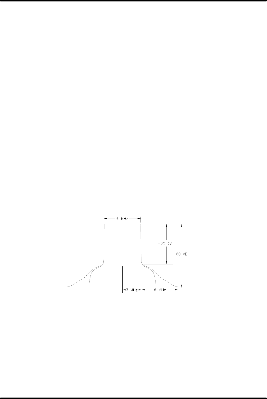
Digital UHF Transmitter Chapter 5, Detailed Alignment Procedures
DT835A, Rev. 1 5-4
5.2.2 IF Phase Corrector Adjustment
As shipped, the exciter was preset to
include linearity (gain vs. level) and
phase pre-distortion. The pre-distortion
was adjusted to approximately
compensate the corresponding non-linear
distortions of the amplifier trays.
Locate (A9) the IF phase corrector board
(1227-1250) mounted in the UHF exciter
tray. Because the amplitude correction
portion of the board is not utilized in this
configuration, the jumper W3 on J10
should be in the disable position and R35
and R31 should be fully counter-
clockwise (CCW). R68 is the range
adjustment and should be set in the
middle. The phase correction
enable/disable jumper W2 on J9 should
be in the Enable position to ground.
Set up a spectrum analyzer with 30 kHz
resolution bandwidth and 30 kHz
modulation bandwidth to monitor the
intermodulation products of the RF
output signal. A typical digital spectrum
is shown in Figure 5-1. There are three
corrector stages on the IF phase
corrector board, each with a magnitude
and a threshold adjustment which are
adjusted as needed to correct for any
intermod problems. Adjust the R3
threshold for the cut in point of the
correction and the R7 magnitude for the
amount of the correction that is needed.
The jumper W1 on J8 is set to give the
desired polarity of the correction shaped
by the threshold R11 and magnitude R15
adjustments. After setting the polarity,
adjust the R11 threshold for the cut in
point of the correction and the R15
magnitude for the amount of the
correction that is needed. Finally, adjust
the R19 threshold for the cut in point of
the correction and the R23 magnitude for
the amount of the correction that is
needed. The above pots are adjusted for
the greatest separation between the
digital signal and the intermod at the
channel edges.
Figure 5-1: Typical Digital Spectrum

Digital UHF Transmitter Chapter 5, Detailed Alignment Procedures
DT835A, Rev. 1 5-5
5.2.3 (A15-A1) UHF Generator
Board (1565-1109)
The (A15-A1) UHF generator board is
mounted in (A15) the UHF generator
enclosure. This procedure should be
performed to align this board.
In the Manual Adjust Set Up position, W1
on J4 between Pins 2 & 3, on (A13) the
PLL board (1286-1104), adjust R12 for
–2.5 volts at J6 pin 2.
Connect J1, the sample output of the
section of the UHF generator board, to a
spectrum analyzer, tuned to the crystal
frequency, and peak tuning capacitors C6
and C18 for maximum output. Also tune
L2 and L4 for maximum output. The
output level should be about +5 dBm.
The channel oscillator should maintain an
oven temperature of 50° C.
If a spectrum analyzer is not available,
connect a digital voltmeter (DVM) to TP1
on the UHF generator board. Tune
capacitor C32 for maximum voltage at
TP1.
Connect J2, the sample output of the
channel oscillator, to a suitable counter
and tune C11, the coarse adjust, to the
crystal frequency. The fine frequency is
controlled by the external PLL circuit
when in the Auto mode.
Caution: Do not re-peak C32. This
can change the output level.
Connect a spectrum analyzer to J2, the
output jack of the board.
Tune C32, C34, C38, C40, C44, and C46
for maximum output. Re-adjust all of the
capacitors to minimize the seventh and
the ninth harmonics of the channel
oscillator frequency. They should be
down at least -30 dB without affecting
the output of the UHF generator board.
If a spectrum analyzer is not available, a
DC voltmeter can be used. When a
voltmeter is used, the harmonic
frequencies must be minimized to
prevent interference with other channels.
While monitoring each test point with a
DC voltmeter, maximize each test point
by tuning the broadband multipliers in
the following sequence:
• Monitor TP1 with a DVM and tune C32
for maximum (typical 0.6 VDC).
• Monitor TP2 and tune C34 and C38
for maximum (typical 1.2 VDC).
• Monitor TP3 and tune C40 and C44
for maximum (typical 2.0 VDC).
• Monitor TP4 and tune C46 for
maximum.
• Repeak C40 and C38 while
monitoring TP4 (typical 3.5 VDC).
• The typical output level is +15 dBm.
5.2.4 (Optional) (A14-A1) 10-MHz
Reference Generator Board (1519-
1126)
Monitor J1 with a spectrum analyzer.
Adjust C12 for a maximum 10-MHz
signal.
Attach a frequency counter. Tune C3 for
a coarse frequency adjustment close to
10 MHz and C2 for exactly 10 MHz. Re-
adjust C12 for peak signal amplitude at
J1 using the spectrum analyzer. Adjust
R15 to maintain a constant crystal
temperature of 50° C.
5.2.5 (A13) PLL Board (1286-1104)
Check that Jumper W1 on J4 is between
Pins 2 and 3 and that R12 is adjusted for
–2.5 volts at J6-2. Adjust C11 on the
(A15-A1) UHF generator board (1565-
1109) for the correct channel oscillator
frequency. Monitor J10 on the board.
Install jumper W1 between J4-1 and J4-
2. With switches SW1, SW2, and SW3 in
the positions shown in Table 5-5 (refer
to the PLL board schematic [1286-
3104]), the PLL Unlock LED should go
out.
Digital UHF Transmitter Chapter 5, Detailed Alignment Procedures
DT835A, Rev. 1 5-6
Table 5-5: Switch Positions
SWITCH POSITION
SW1-8 N5
SW1-7 N4
SW1-6 N3
SW1-5 N2
SW2-8 N1
SW2-7 N0
SW2-6 A5
SW2-5 A4
SW3-8 A3
SW3-7 A2
SW3-6 A1
SW3-5 A0
Table 5-6 shows the proper switch positions according to channel frequencies.
Note: N7 and N6 are fixed values and can not be programmed.
Table 5-6: Switch Positions for Channel Frequencies
CHANNEL
FREQUENCY
(MHz) N N7-N0 A A5-A0
14 517 64 01000000 40 101000
15 523 65 01000001 24 011000
16 529 66 01000010 8 001000
17 535 66 01000010 56 111000
18 541 67 01000011 40 101000
19 547 68 01000100 24 011000
20 553 69 01000101 8 001000
21 559 69 01000101 56 111000
22 565 70 01000110 40 101000
23 571 71 01000111 24 011000
24 577 72 01001000 8 001000
25 583 72 01001000 56 111000
26 589 73 01001001 40 101000
27 595 74 01001010 24 011000
28 601 75 01001011 8 001000
29 607 75 01001011 56 111000
30 613 76 01001100 40 101000
31 619 77 01001101 24 011000
32 625 78 01001110 8 001000
33 631 78 01001110 56 111000
34 637 79 01001111 40 101000
35 643 80 01010000 24 011000
36 649 81 01010001 8 001000
37 655 81 01010001 56 111000
38 661 82 01010010 40 101000
39 667 83 01010011 24 011000
Digital UHF Transmitter Chapter 5, Detailed Alignment Procedures
DT835A, Rev. 1 5-7
CHANNEL
FREQUENCY
(MHz) N N7-N0 A A5-A0
40 673 84 01010100 8 001000
41 679 84 01010100 56 111000
42 685 85 01010101 40 101000
43 691 86 01010110 24 011000
44 697 87 01010111 8 001000
45 703 87 01010111 56 111000
46 709 88 01011000 40 101000
47 715 89 01011001 24 011000
48 721 90 01011010 8 001000
49 727 90 01011010 56 111000
50 733 91 01011011 40 101000
51 739 92 01011100 24 011000
52 745 93 01011101 8 001000
53 751 93 01011101 56 111000
54 757 94 01011110 40 101000
55 763 95 01011111 24 011000
56 769 96 01100000 8 001000
57 775 96 01100000 56 111000
58 781 97 01100001 40 101000
59 787 98 01100010 24 011000
60 793 99 01100011 8 001000
61 799 99 01100011 56 111000
62 805 100 01100100 40 101000
63 811 101 01100101 24 011000
64 817 102 01100110 8 001000
65 823 102 01100110 56 111000
66 829 103 01100111 40 101000
67 835 104 01101000 24 011000
68 841 105 01101001 8 001000
69 847 105 01101001 56 111000
5.3 (A1-A6) UHF Amplifier Trays
(1294-1112, low band/1294-1113,
mid band/ 1294-1114, high band;
Appendix C)
The UHF Amplifier Trays are located in
the 2-3kW Amplifier Arrays.
The UHF amplifier trays (1294-1112, low
band/1294-1113, mid band/ 1294-1114,
high band) have been adjusted at the
factory to meet all specifications,
including phase adjustment, to match the
multiple trays in an amplifier array when
they are combined. The trays should not
need to be adjusted to attain normal
operation. Any adjustments to the boards
in the trays should be performed in the
Manual Gain position, with S1 on (A8)
the amplifier control board (1265-1414)
in Manual. The idling current for the
amplifier boards are adjusted with no RF
drive applied. S1 should be in the Auto
AGC position for the normal operation of
the transmitter.
Connect a dummy load with a rating of a
least 300 watts to J2, the RF output jack
of the tray being aligned.

Digital UHF Transmitter Chapter 5, Detailed Alignment Procedures
DT835A, Rev. 1 5-8
5.3.1 (A2-A1) Variable Gain/Phase
Board (1265-1425; Appendix D)
The board is mounted in (A2) the
variable gain/phase enclosure. The board
has an AGC adjustable gain of 0 to 20
dB.
5.3.2 (A3-A1) 1-Watt UHF Amplifier
Board (1227-1303; Appendix D)
The board is mounted in (A3) the 1-watt
UHF amplifier enclosure. There are no
adjustments to this board; it has
approximately 10 dB of gain.
5.3.3 (A1) UHF Filter (1007-1101;
Appendix D)
Apply a multiburst test signal to the
transmitter. Monitor J2 with a spectrum
analyzer and tune C1 and C3 for peak
output with a flat-frequency response.
5.3.4 (A4-A1) Single Stage Amplifier
Assembly, Class A (1265-1418, low
band/1265-1416, mid band/1265-
1417, high band; Appendix B)
This assembly is made from a generic
single stage amplifier board, class A
(1265-1415) with a frequency
determining kit.
The generic single stage amplifier board
operates class A and has a gain of
approximately 11 dB. The bias of the
transistor is set by the on-board biasing
circuit. Adjust R6 for 5 amps of idle
current, no RF drive applied. Connect a
voltage meter across E1 and E2 on the
amplifier protection board and move
switch S1 to the I1 position; adjust R6
for a reading of 50 mV. Connect a sweep
test signal to J1, the RF input jack of the
UHF amplifier tray and monitor the
output of the board at J2 with a padded-
input spectrum analyzer. Tune capacitor
C5 for peak output and then tune C6 for
peak output power with a flat-frequency
response at J2.
5.3.5 (A4-A2) Coupler Board
Assembly (1227-1316; Appendix D)
There are no adjustments to this board.
5.3.6 (A4-A3) Dual Stage Amplifier
Assembly, Class AB (1265-1413, low
band/1265-1411, mid band/1265-
1420, high band; Appendix D)
This assembly is made from a generic
dual stage amplifier board, class AB
(1265-1404) with a frequency
determining kit.
The generic dual stage amplifier board
operates class AB and has a gain of
approximately 9 dB. The biases of the
transistors are set by the on-board
biasing circuits. Adjust R106 and R206
100 mA digital of idle current per side, no
RF drive applied. Connect a voltage
meter across E1 and E2 on the amplifier
protection board and move switch S1 to
the I3 position; adjust R106 for a reading
of 1 mV digital. Move switch S1 to the I2
position and adjust R206 for a reading of
1 mV digital. Depending on the linearity
of tray, these transistors may have 50
mA digital of bias. Connect a sweep test
signal to J1, the RF input jack of the UHF
amplifier tray, and monitor the output of
the board at J2 with a padded input to a
spectrum analyzer. Tune capacitors C105
and C205 for peak output and then tune
C119 and C219 for peak output with a
flat-frequency response and minimum
current at J2.
5.3.7 (A5-A1) 4-Way Splitter
Assembly (1265-1432; Appendix D)
There are no adjustments to this
assembly.
5.3.8 (A5-A2, A5-A3, A5-A4, and A5-
A5) Dual Stage Amplifier Assemblies,
Class AB (1265-1439, low
band/1265-1440, mid band/1265-
1441, high band; Appendix D)
Each board is made from a generic dual
stage amplifier board, class AB (1265-

Digital UHF Transmitter Chapter 5, Detailed Alignment Procedures
DT835A, Rev. 1 5-9
1404) with a frequency determining kit.
These boards operate class AB and have
a gain of approximately 9 dB. The idling
current for each of the transistors is set
to 100 mA digital.
To adjust the idling currents, no RF
applied to the tray, of the devices on
(A5-A2) the amplifier board, connect a
voltage meter across E1 and E2 on the
amplifier protection board and move
switch S1 to the I5 position; adjust R106
for a reading of 1 mV digital. Move switch
S1 to the I4 position and adjust R206 for
a reading of 1 mV digital.
Connect a sweep test signal to J1, the RF
input jack of the UHF amplifier tray. On
(A5-A2) the amplifier board, tune
capacitors C105 and C205 for peak
output power and then tune C119 and
C219 for peak output power with a flat-
frequency response and minimum
current.
To adjust the idling currents, no RF
applied to the tray, of the devices on
(A5-A3) the amplifier board, connect a
voltage meter across E1 and E2 on the
amplifier protection board and move
switch S1 to the I7 position; adjust R106
for a reading of 1 mV digital. Move switch
S1 to the I6 position and adjust R206 for
a reading of 1 mV digital.
Connect a sweep test signal to J1, the RF
input jack of the UHF amplifier tray. On
the (A5-A3) dual stage amplifier board,
tune capacitors C105 and C205 for peak
output power and then tune C119 and
C219 for peak output power with a flat-
frequency response and minimum
current.
To adjust the idling currents, no RF
applied to the tray, of the devices on the
(A5-A4) amplifier board, connect a
voltage meter across E1 and E2 on the
amplifier protection board and move
switch S1 to the I9 position; adjust R106
for a reading of 1 mV digital. Move switch
S1 to the I8 position and adjust R206 for
a reading of 1 mV digital.
Connect a sweep test signal to J1, the RF
input jack of the UHF amplifier tray. On
the (A5-A4) amplifier board, tune
capacitors C105 and C205 for peak
output power and then tune C119 and
C219 for peak output power with a flat-
frequency response and minimum
current.
To adjust the idling currents, no RF
applied to the tray, of the devices on the
(A5-A5) amplifier board, connect a
voltage meter across E1 and E2 on the
amplifier protection board and move
switch S1 to the I11 position; adjust
R106 for a reading of 1 mV digital. Move
switch S1 to the I10 position and adjust
R206 for a reading of 1 mV digital.
Connect a sweep test signal to J1, the RF
input jack of the UHF amplifier tray. On
the (A5-A5) amplifier board, tune
capacitors C105 and C205 for peak
output power and then tune C119 and
C219 for peak output power with a flat-
frequency response and minimum
current.
5.3.9 (A5-A6) 4-Way Combiner
Assembly (1265-1428, low
band/1265-1429, mid band/1265-
1430, high band; Appendix D)
This assembly contains (A5-A6-A1) a 4-
way combiner board. There are no
adjustments to the board.
5.3.10 (A5-A6-A2) Circulator
There are no adjustments to the
circulator.
5.3.11 (A6-A1) Dual Peak Detector
Board, Single Supply (1227-1333;
Appendix D)
The dual peak detector board is mounted
in (A6) a dual peak detector enclosure.
There are no adjustments to the board.

Digital UHF Transmitter Chapter 5, Detailed Alignment Procedures
DT835A, Rev. 1 5-10
5.3.12 (A7) Amplifier Protection
Board (1265-1412; Appendix D)
There are no adjustments to this board.
5.3.13 (A8) Amplifier Control Board
(1265-1414; Appendix D)
To check the operation of the overdrive
circuit, increase the gain pot of the UHF
amplifier tray to approximately 110%.
The Overdrive LED DS2 should light and
the output power should not increase
above the 110% level. If the LED does
not light, adjust R71 the overdrive
threshold as needed until the LED lights.
5.3.14 (A12) +26.5V/2000W
Switching Power Supply
This switching power supply does not
contain any customer-repairable items. If
the power supply should malfunction, do
not attempt to repair the power supply
without first consulting the Axcera Field
Support Department. The power supply
is adjusted to provide an output of +26.5
VDC.
5.3.15 Calibration of Output Power,
Reflected Power and VSWR Cutback
of the tray
To calibrate the forward output power
reading of the tray. Place a calibrated
coupler, average power wattmeter and
dummy load of at least 300 watts at the
output of the tray that is to be calibrated.
Switch the front panel meter to the %
Output Power position. Preset R16,
manual gain, on (A8) the amplifier
control board fully CCW. Move switch S1
on the amplifier control board to the
Manual position. Insert a digital test
signal and adjust R16 for 300 watts 64
QAM or 8-VSB digital on the wattmeter.
Calibrate the front panel output power
meter to 100% by adjusting the pot, R2,
forward calibration, located on the
amplifier control board. The forward
output power reading of the tray is now
calibrated.
To calibrate the reflected output power
reading and VSWR cutback of the tray.
Reduce manual gain pot R16 to a 50%
reading on the front panel meter in the
% Output Power position. Turn off the
tray. Remove the load from the output
of the tray and switch the front panel
meter to the Reflected Output Power
position. Switch on the tray. Adjust
reflected power adjust pot R22 on the
amplifier control board to a 50% reading.
Then adjust R29, the VSWR threshold
cutback pot, on the amplifier control
board until the VSWR Cutback LED DS1
on the front panel just lights. This sets
up the VSWR cutback circuitry.
After this calibration is completed,
reconnect the tray to the system and
move switch S1 on the amplifier control
board to the Automatic Gain Control
position. This is the normal operating
position for the switch.
The UHF amplifier tray is now aligned,
calibrated, and ready for normal
operation. Repeat as needed for the
other Amplifier Trays in the System
5.4 Phase and Gain Adjustment of
the UHF Amplifier Trays in each
Amplifier Array
Switch the Transmitter to Standby and
switch Off the Main AC Circuit Breaker
located on each of the AC Distribution
Assemblies in the Amplifier Array
Assemblies. Switch Off all the AC Circuit
Breakers, located on the AC Distribution
Assembly, for the individual Amplifier
Trays.
1. Adjust all gain controls located on
the UHF Amplifier Trays full CCW.
2. Switch On the Main AC Circuit
Breaker for the Side A Amplifier
Array Assembly and switch On the
AC Circuit Breaker for Amplifier #1.
3. Place the Transmitter in Operate
and adjust the Gain control on the

Digital UHF Transmitter Chapter 5, Detailed Alignment Procedures
DT835A, Rev. 1 5-11
Amplifier Tray for 50% output
power and adjust the Phase control
to mid range.
4. Monitor the output power of the
Transmitter by connecting a
Spectrum Analyzer to the Sample
Jack located on the Metering Panel.
Adjust the Spectrum Analyzer for
Zero Span operation. The power
could be monitored by watching the
meters on the panel but the power
change is easier to see on the
analyzer.
5. Turn On the AC to Amplifier Tray #2
and adjust its' output power to
50%.
6. While monitoring the output power
of the Transmitter, adjust the Phase
Control on amplifier tray #2 until
the power reaches a peak. If the
Phase adjust reaches its end of
travel, add a 2 inch cable to the RF
Input (J1) of amplifier tray #2. Re-
adjust the Phase to peak the
System output power. If the Phase
Control again reaches its end of
travel before a peak in power is
reached, remove the 2 inch cable
and add a 3 inch cable to J1 of
amplifier tray #2 and readjust
phase for peak output power. The
adding of cables should be done
during the adjustment anytime the
range of the phase adjust needs
extended.
7. Repeat steps 5 and 6 for the
remaining Amplifiers.
8. Increase the output power on
Amplifier #1 and Amplifier #2 to
90%.
9. Adjust the Phase Control on
Amplifier #2 to peak the System
output power.
10. Increase the output power on
Amplifier #3 to 90% and adjust the
Amplifier #3 Phase control for
maximum System output power.
11. Increase the output power on
Amplifier #4 to 90% and adjust the
Amplifier #4 Phase control for
maximum System output power.
12. Increase the output power on
Amplifier #5, if present, to 90%
and adjust the Amplifier #5 Phase
control for maximum System output
power.
13. Increase the output power on
Amplifier #6, if present, to 90%
and adjust the Amplifier #6 Phase
control for maximum System output
power.
14. Monitor the Reflected Power on all
of the UHF Amplifier Trays. The
Reflected Power should read <5%.
If an amplifier is showing high
reflected power adjust the Phase
control to minimize Reflected
Power. Be careful not to increase
Reflected Power on the other
Amplifier Trays. The Amplifier
Trays should interact in such a way
that the phasing of any one
Amplifier will affect the Reflected on
the other Amplifiers.
5.5 Calibration of the Side A and Side
B Amplifier Arrays Forward Output
Power Level
Note: Perform the following
procedure only if the power
calibration is suspect.
Set up the transmitter for the appropriate
average output power level out of the
Side A Cabinet. A calibrated coupler and
average power wattmeter must be used
to measure the digital power level.
Side A Forward Power Calibration.
In (A6) the Metering Control Panel,
located in the UHF Exciter Cabinet, find
the (A9) Dual Peak Detector Board

Digital UHF Transmitter Chapter 5, Detailed Alignment Procedures
DT835A, Rev. 1 5-12
(1159965). Adjust R9 for 100% on the
Side A Power Meter.
Side B Forward Power Calibration.
In (A6) the Metering Control Panel,
located in the UHF Exciter Cabinet, find
the (A8) Dual Peak Detector Board
(1159965). Adjust R9 for 100% on the
Side B Power Meter.
5.6 Calibration of the Side A and Side
B Amplifier Arrays Reflected Output
Level
Monitor the Side A Power Meter, in the
Forward Power position, and turn the
power adjust pot, located on the (A4)
Phase/Gain Tray, to 20%. Move the
cable connected to J3, located on the
(A8) Output Coupler, inside the Side A
Amplifier Cabinet, to Jack J6 and the
cable on J6 to J3. Adjust R10 on (A9)
the Dual Peak Detector Board, located in
the Metering Control Panel, for a 20%
reading in the Reflected Power position.
At this 20% reference power reading, the
VSWR LED mounted on the front panel of
the Exciter Tray should be illuminated. If
the VSWR LED is not illuminated, adjust
R5 on (A18) the Detector Threshold
Board, located in the Metering Control
Panel, until the LED just begins to turn
on. Turn the power adjust pot slightly
CCW and the LED should go out. Turn the
pot CW until the LED just begins to turn
on. The reflected output power for the
amplifier array is now calibrated. Move
the cable connected to J6 back to J3 and
the cable on J3 back to J6, on the (A8)
Coupler.
Monitor the Side B Power Meter, in the
Forward Power position, and turn the
power adjust pot, located on the (A5)
Phase/Gain Tray for Side B, to 20%.
Move the cable connected to J3, located
on the (A8) Output Coupler, inside the
Side B Amplifier Cabinet, to Jack J6 and
the cable on J6 to J3. Adjust R10 on the
(A8) Dual Peak Detector Board, located
in the Metering Control Panel, for a 20%
reading in the Reflected Power position.
At this 20% reference power reading, the
VSWR LED mounted on the front panel of
the Exciter Tray should be illuminated. If
the VSWR LED is not illuminated, adjust
R12 on (A18) the Detector Threshold
Board, located in the Metering Control
Panel, until the LED just begins to turn
on. Turn the power adjust pot slightly
CCW and the LED should go out. Turn the
pot CW until the LED just begins to turn
on. The reflected output power for Side B
is now calibrated. Move the cable
connected to J6 back to J3 and the cable
on J3 back to J6, on the (A8) Coupler.
5.7 Phase and Gain Adjustment
Procedure for entire Amplifier Array
Assembly
Begin the alignment with all Amplifier
Trays up and running. Monitor the Reject
Power by setting the Combined Metering
switch to the Reject position and
adjusting the Phase Control on either, or
both, of the Phase/Gain Modules to
minimize the Reject reading.
Adjust the Amplifier Gain controls so that
all amplifiers have equal output power.
The Gain control on the Phase/Gain Tray
can be used to balance the output power
between Sides A and B. This adjustment
has a 10% range. If the end of its' range
is reached, you must adjust the gain of
each amplifier in the Amplifier Side to
balance the power of each Side.
5.8 Calibration of the Forward
Output Power Level of the
Transmitter
Note: - Perform the following only if the
power calibration is suspect.
Set the Transmitter up for the
appropriate Average Output Power Level.
Using a calibrated coupler on the
combined RF output line and an HP
power meter (or an equivalent

Digital UHF Transmitter Chapter 5, Detailed Alignment Procedures
DT835A, Rev. 1 5-13
measurement instrument), adjust the
output power for a reading of 2000, 2500
or 3000 watts on the true average power
meter. Adjust R28 on (A10) the
visual/aural metering board in the
metering panel for 100% in the %
Combined Output Power position. Set pot
R20 on (A10) the visual/aural metering
board full CCW.
5.9 Calibration of the Reflected
Output Level of the Transmitter
Turn the Power Adjust Pot on the UHF
Exciter to 20% on the Metering Panel
Combined Meter in the Visual Power
position. NOTE: Check that the Jumper
is in Manual on the UHF Upconverter
Board (1265-1310) in the UHF Exciter.
On (A11) the Output Coupler for the
Transmitter, move the cable on J6 to J5
and the Termination on J5 to J6. Adjust
R10 on the (A7) Dual Peak Detector
Board (1159965), in the Metering Panel,
for a 20% reading in the Combined
Reflected Power position. At this 20%
Reference Power reading, the VSWR LED
mounted on the front panel of the UHF
Exciter should be illuminated. If not
adjust R19 on the Detector Threshold
Board, in the Metering Control Panel,
until the VSWR LED just turns On. Turn
the Power Adjust pot slightly CCW and
the LED should go out, turn the pot CW
until the LED just turns On. The
Reflected Output Power is now calibrated.
Switch the Transmitter to Standby. Move
the cable on J5 to J6 and the Termination
on J6 back to J5. Switch the Transmitter
to Operate and adjust the front panel
power pot for 100% Power reading on
the Combined Meter.
5.10 Calibration of the Reject Power
of the Transmitter
Check that the System is operating at
100% Output Power. Remove the AC
power to the Side A Amplifier Array by
switching Off CB1 the Main AC circuit
breaker, located on the AC Distribution
Panel for the Side A Amplifier Array.
Adjust R9 on the (A7) Dual Peak Detector
Board, located in the Metering Control
Panel, for a 25% Power reading in the
reject power position. The Reject power
is now calibrated.
Return CB1, the Main AC circuit breaker
for the Side A Amplifier Array, to the On
position.
The Transmitter is fully aligned and
ready for normal operation
APPENDIX A
SAMPLE LOG REPORT SHEET

Digital UHF Transmitter Appendix A, Sample Log Report Sheet
DT835A, Rev. 1 A-1
(A1) Single UHF Exciter Assembly
(A1-A6) DT835A Metering Panel
Combined
Forward (0 - 120%)=_____________%
Reject (0 - 120%)=_____________% Reflected (0 - 120%)=____________%
(A2) Amplifier Array Side A
Forward (0 - 120%)=____________% Reflected (0 - 120%)=____________%
(A3) Amplifier Array Side B
Forward (0 - 120%)=____________% Reflected (0 - 120%)=____________%
(A1-A1) UHF Exciter Tray
% Exciter (0 - 120%)=___________% ALC (0 - 1 V)=_________________V
(A1-A4) Phase/Gain Tray Side A
% Power (0 - 120%)=____________% ALC (0 - 1 V)=_________________V
(A1-A5) Phase/Gain Tray Side B
ALC (0 - 1 V)=______________V % Power (0 - 120%)=____________%

Digital UHF Transmitter Appendix A, Sample Log Report Sheet
DT835A, Rev. 1 A-2
(A2 and A3) Amplifier Array Assemblies
Two amplifier arrays with four, five or six UHF amplifier trays each
(A2) Side A
(A2-A1) (A2-A2)
AGC Voltage =_________V AGC Voltage =_________V
% Reflected =_________% % Reflected =_________%
% Output Forward =_________% % Output Forward =_________%
Power Supply =__________V Power Supply =__________V
(A2-A3) (A2-A4)
AGC Voltage =_________V AGC Voltage =_________V
% Reflected =_________% % Reflected =_________%
% Output Forward =_________% % Output Forward =_________%
Power Supply =__________V Power Supply =__________V
(A2-A5) (A2-A6)
AGC Voltage =_________V AGC Voltage =_________V
% Reflected =_________% % Reflected =_________%
% Output Forward =_________% % Output Forward =_________%
Power Supply =__________V Power Supply =__________V

Digital UHF Transmitter Appendix A, Sample Log Report Sheet
DT835A, Rev. 1 A-3
(A3) Side B
(A3-A1) (A3-A2)
AGC Voltage =_________V AGC Voltage =_________V
% Reflected =_________% % Reflected =_________%
% Output Forward =_________% % Output Forward =_________%
Power Supply =__________V Power Supply =__________V
(A3-A3) (A3-A4)
AGC Voltage =_________V AGC Voltage =_________V
% Reflected =_________% % Reflected =_________%
% Output Forward =_________% % Output Forward =_________%
Power Supply =__________V Power Supply =__________V
(A3-A5) (A3-A6)
AGC Voltage =_________V AGC Voltage =_________V
% Reflected =_________% % Reflected =_________%
% Output Forward =_________% % Output Forward =_________%
Power Supply =__________V Power Supply =__________V
Date: __________________ Technician: ________________________________
Customer Name: ____________________________ Call Letters: ________________
APPENDIX B
TYPICAL OPERATIONAL READINGS

Digital UHF Transmitter Appendix B, Typical Operational Readings
DT835A, Rev. 1 B-1
(A1) Single UHF Exciter Assembly
(A1-A6) DT835A Metering Panel
Combined
Forward (0 - 120%) = ≈100 %
Reject (0 - 120%) = <5% Reflected (0 - 120%) = <5%
(A2) Amplifier Array Side A
Forward (0 - 120%) = The level as needed
to attain the desired output power of the
transmitter
Reflected (0 - 120%) = <5%
(A3) Amplifier Array Side B
Forward (0 - 120%) = The level as needed
to attain the desired output power of the
transmitter
Reflected (0 - 120%) = <5%
(A1-A1) UHF Exciter Tray
% Exciter (0 - 120%) = ≈ 70 % ALC (0 - 1 V) = ≈0.8 V
(100%=+10 dBm 64 QAM or 8-VSB digital
(A1-A4) Phase/Gain Tray Side A
% Power (0 - 120%) = ≈ 50% ALC (0 - 1 V) = 0.6 - 1 V typical
(A1-A5) Phase/Gain Tray Side B
% Power (0 - 120%) = ≈ 50% ALC (0 - 1 V) = 0.6-1 V typical

Digital UHF Transmitter Appendix B, Typical Operational Readings
DT835A, Rev. 1 B-2
(A2 and A3) Amplifier Array Assemblies
Two amplifier arrays, each with four, five or six UHF amplifier trays
(A2) Side A
(A2-A1) (A2-A2)
AGC Voltage = 1 V - 2 V AGC Voltage = 1 V - 2 V
% Reflected = <5% with all trays operating % Reflected = <5% with all trays operating
% Output Forward = The level is as needed
to attain the desired output power from the
transmitter
% Output Forward = The level is as needed
to attain the desired output power from the
transmitter
Power Supply = 26.5 V Power Supply = 26.5 V
(A2-A3) (A2-A4)
AGC Voltage = 1 V - 2 V AGC Voltage = 1 V - 2 V
% Reflected = <5% with all trays operating % Reflected = <5% with all trays operating
% Output Forward = The level is as needed
to attain the desired output power from the
transmitter
% Output Forward = The level is as needed
to attain the desired output power from the
transmitter
Power Supply = 26.5 V Power Supply = 26.5 V
(A2-A5) (A2-A6)
AGC Voltage = 1 V - 2 V AGC Voltage = 1 V - 2 V
% Reflected = <5% with all trays operating % Reflected = <5% with all trays operating
% Output Forward = The level is as needed
to attain the desired output power from the
transmitter
% Output Forward = The level is as needed
to attain the desired output power from the
transmitter
Power Supply = 26.5 V Power Supply = 26.5 V

Digital UHF Transmitter Appendix B, Typical Operational Readings
DT835A, Rev. 1 B-3
(A3) Side B
(A3-A1) (A3-A2)
AGC Voltage = 1 V - 2 V AGC Voltage = 1 V - 2 V
% Reflected = <5% with all trays operating % Reflected = <5% with all trays operating
% Output Forward = The level is as needed
to attain the desired output power from the
transmitter
% Output Forward = The level is as needed
to attain the desired output power from the
transmitter
Power Supply = 26.5 V Power Supply = 26.5 V
(A3-A3) (A3-A4)
AGC Voltage = 1 V - 2 V AGC Voltage = 1 V - 2 V
% Reflected = <5% with all trays operating % Reflected = <5% with all trays operating
% Output Forward = The level is as needed
to attain the desired output power from the
transmitter
% Output Forward = The level is as needed
to attain the desired output power from the
transmitter
Power Supply = 26.5 V Power Supply = 26.5 V
(A3-A5) (A3-A6)
AGC Voltage = 1 V - 2 V AGC Voltage = 1 V - 2 V
% Reflected = <5% with all trays operating % Reflected = <5% with all trays operating
% Output Forward = The level is as needed
to attain the desired output power from the
transmitter
% Output Forward = The level is as needed
to attain the desired output power from the
transmitter
Power Supply = 26.5 V Power Supply = 26.5 V
APPENDIX C
ASSEMBLY DRAWINGS

Digital UHF Transmitter Appendix C, Assembly Drawings and Parts Lists
DT835A, Rev. 1 C-1
DT835A
Transmitter Racking Plan.....................................................................1142231
Transmitter Interconnect .....................................................................1056920
UHF Exciter Assembly
Interconnect.......................................................................................1056919
AC Distribution Assembly, Exciter Assembly
Interconnect....................................................................................1245-8500
UHF Digital Exciter Tray
Block Diagram....................................................................................1300494
Interconnect.......................................................................................1300491
Variable Phase/Gain Tray
Block Diagram.................................................................................1245-3200
Interconnect....................................................................................1245-8200
Metering Panel
Interconnect.......................................................................................1061458
Amplifier Array Assembly, 2 required for Digital Transmitter
Block Diagram ............................................................................. 1278-3300
Interconnect................................................................................ 1278-8300
AC Distribution Assembly, one in each Amplifier Array
Interconnect....................................................................................1278-8200
UHF Amplifier Tray, 4, 5 or 6 in each Amplifier Array Assembly
Block Diagram.................................................................................1281-3100
Interconnect....................................................................................1281-8100
APPENDIX C
SUBASSEMBLY DRAWINGS

Digital UHF Transmitter Appendix D, Subassembly Drawings and Parts Lists
DT835A, Rev. 1 D-1
UHF Filter
Schematic........................................................................................1007-3101
±12V Power Supply Board
Schematic........................................................................................1062-3013
General Purpose +12V Power Supply Board
Schematic........................................................................................1128-3504
Channel Oscillator Board, Dual Oven
Schematic........................................................................................1145-3201
Splitter Board
Schematic........................................................................................1181-3002
IF Delay Equalizer Board
Schematic......................................................................................... 1197-3112
x8 Multiplier Board
Schematic........................................................................................1227-3002
IF Phase Corrector Board
Schematic........................................................................................1227-3250
1 Watt Amplifier Board
Schematic........................................................................................1227-3303
Coupler Board Assembly
Schematic........................................................................................1227-3316
Dual Peak Detector Board, Single Supply
Schematic........................................................................................1227-3333
Transmitter Control Board
Schematic........................................................................................1245-3101
Variable Gain/Phase Board
Schematic........................................................................................1245-3201
Metering Board
Schematic........................................................................................1245-3202
+15V/-12V Power Supply Board
Schematic........................................................................................1245-3203
Detector Threshold Board
Schematic........................................................................................1245-3402
ALC Board, NTSC
Schematic........................................................................................1265-3305

Digital UHF Transmitter Appendix D, Subassembly Drawings and Parts Lists
DT835A, Rev. 1 D-2
Visual/Aural Metering Board
Schematic........................................................................................1265-3309
UHF Upconverter Board
Schematic........................................................................................1265-3310
Transmitter Control Board
Schematic........................................................................................1265-3311
+12V(4A)/-12V(1A) Power Supply Board
Schematic........................................................................................1265-3312
Dual Stage Amplifier Assembly, Class AB, Mid Band
Made from a Generic Dual Stage Amplifier Board, Class AB (1265-1404).
Schematic........................................................................................1265-3411
Amplifier Protection Board
Schematic........................................................................................1265-3412
Dual Stage Amplifier Assembly, Class AB, Low Band
Made from a Generic Dual Stage Amplifier Board, Class AB (1265-1404).
Schematic........................................................................................1265-3413
Amplifier Control Board
Schematic........................................................................................1265-3414
Single Stage Amplifier Assembly, Class A, Mid Band
Made from a Generic Dual Stage Amplifier Board, Class A (1265-1415).
Schematic........................................................................................1265-3416
Single Stage Amplifier Assembly, Class A, High Band
Made from a Generic Dual Stage Amplifier Board, Class A (1265-1415).
Schematic........................................................................................1265-3417
Single Stage Amplifier Assembly, Class A, Low Band
Made from a Generic Dual Stage Amplifier Board, Class A (1265-1415).
Schematic........................................................................................1265-3418
Dual Stage Amplifier Assembly, Class AB, High Band
Made from a Generic Dual Stage Amplifier Board, Class AB (1265-1404).
Schematic........................................................................................1265-3420
Variable Gain/Phase Board
Schematic........................................................................................1265-3425
Dual Stage Amplifier Assembly, Class AB, Low Band
Made from a Generic Dual Stage Amplifier Board, Class AB (1265-1404).
Schematic........................................................................................1265-3439
Dual Stage Amplifier Assembly, Class AB, Mid Band
Made from a Generic Dual Stage Amplifier Board, Class AB (1265-1404).
Schematic........................................................................................1265-3440

Digital UHF Transmitter Appendix D, Subassembly Drawings and Parts Lists
DT835A, Rev. 1 D-3
Dual Stage Amplifier Assembly, Class AB, High Band
Made from a Generic Dual Stage Amplifier Board, Class AB (1265-1404).
Schematic........................................................................................1265-3441
Combiner Reject Load Board
Schematic........................................................................................1278-3311
PLL Board
Schematic........................................................................................1286-3104
Output Distribution Amplifier Board (2 per unit)
Schematic........................................................................................1500-3602
Dual Average Detector Board
Schematic........................................................................................1510-3105
10 MHz Reference Generator Board
Schematic........................................................................................1519-3126
IF Input Equalizer Board, 44 MHz
Schematic........................................................................................1555-3219
Dual Peak Detector Board, SMT
Schematic........................................................................................1555-3270
Transmitter Control Board
Schematic...........................................................................................1061195
5 Section Delay Equalizer Board, 44 MHz
Schematic...........................................................................................1072141
Serial Port Interface Board
Schematic...........................................................................................1075976
Dual Peak Detector Board
Schematic...........................................................................................1159976
APPENDIX D
DT835A SYSTEM SPECIFICATIONS
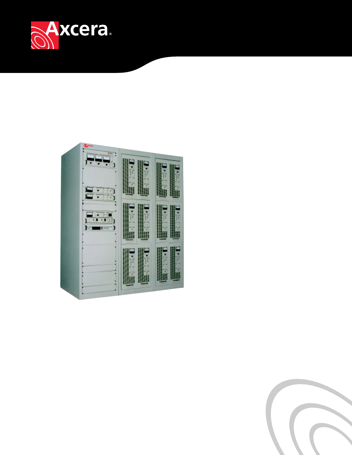
Solid State DTV Transmitters
DT835A-3, DT835A-4, DT835A-5, DT835A-6
The DT800A Series is a full line of low and
medium power UHF DTV transmitters. This
time proven design offers high performance
and simplicity in a very compact unit. Solid
state digital output power levels are available
up to 3 kilowatts average while tube type
versions offer up to 5 kilowatts average. To
ensure optimum performance, these
transmitters benefit from years of experience
in DTV modulator, exciter, and solid-state
amplifier design and manufacturing.
Designed for high reliability and unattended
operation, these products utilize parallel
amplifier designs with a high level of
protection circuitry. Features such as VSWR
cutback, overdrive protection, over-
temperature protection, dedicated power
supplies and cooling, and output circulators in
each amplifier ensure on-air reliability.
Convenient system monitoring is achieved
through front panel samples, status indicators
and metering, most of which are remote
controllable.

B0014 0502 R0
DT835A-3, DT835A-4, DT835A-5, DT835A-6
Performance
Output Power (average) 1500 / 2000 / 2500 / 3000 Watts
Frequency Range1470 to 806MHz
Output Impedance 50 ohms
Frequency Stability ±1KHz (max 30 day variation)
w/Precise Frequency Option ±2Hz
Regulation of RF Output Power 3%
Out of Band - Compliant with FCC Mask2
Channel Edge ±500KHz -47dB or better
6MHz from Channel Edge -110dB or better
Signal to Noise (SNR) 27dB or better
Data Interface
Input Rate 19.39Mbps. 6Hz channel
Input Interface SMPTE 310M, Serial Differential ECL and TTL
Test Signals Staircase, VSB Pilot, Zero Pilot, Average Power Pilot, Nyquist
Waveform
General
Operational Temperature Range 0 to +50°C, derate 2°C/1000ft
Maximum Altitude38500 feet (2600 m) AMSL
Operational Humidity Range 0% to 95% non-condensing
Transmitter Dimensions (W x D x H)
DT835A-3 44” x 34” x 80”
DT835A-4, 5, 6 66” x 34” x 80”
Weight 1050 / 1350 / 1500 / 1650 lbs
RF Load Impedance 50 ohms
Line Voltage4230V ±10%, 1 or 3 phase, 50/60Hz
Power Consumption
System Power 10.5kW / 13.5kW / 17kW / 20.5kW
Power Factor 0.95
Options
Dual Exciter with Automatic Switcher
AC Surge Protector
Precise Frequency Kit
Spare Parts Kit
1 Other Frequencies - Consult Factory
2 Measured in 30KHz RBW, relative to total average power
3 Above 8,500 feet - Consult Factory
4 Other Voltages - Consult Factory